JP2011145391A - Electrophoretic display device and electronic equipment - Google Patents
Electrophoretic display device and electronic equipment Download PDFInfo
- Publication number
- JP2011145391A JP2011145391A JP2010005006A JP2010005006A JP2011145391A JP 2011145391 A JP2011145391 A JP 2011145391A JP 2010005006 A JP2010005006 A JP 2010005006A JP 2010005006 A JP2010005006 A JP 2010005006A JP 2011145391 A JP2011145391 A JP 2011145391A
- Authority
- JP
- Japan
- Prior art keywords
- substrate
- electrophoretic
- electrode
- display device
- pixel
- Prior art date
- Legal status (The legal status is an assumption and is not a legal conclusion. Google has not performed a legal analysis and makes no representation as to the accuracy of the status listed.)
- Withdrawn
Links
Images


Classifications
-
- G—PHYSICS
- G02—OPTICS
- G02F—OPTICAL DEVICES OR ARRANGEMENTS FOR THE CONTROL OF LIGHT BY MODIFICATION OF THE OPTICAL PROPERTIES OF THE MEDIA OF THE ELEMENTS INVOLVED THEREIN; NON-LINEAR OPTICS; FREQUENCY-CHANGING OF LIGHT; OPTICAL LOGIC ELEMENTS; OPTICAL ANALOGUE/DIGITAL CONVERTERS
- G02F1/00—Devices or arrangements for the control of the intensity, colour, phase, polarisation or direction of light arriving from an independent light source, e.g. switching, gating or modulating; Non-linear optics
- G02F1/01—Devices or arrangements for the control of the intensity, colour, phase, polarisation or direction of light arriving from an independent light source, e.g. switching, gating or modulating; Non-linear optics for the control of the intensity, phase, polarisation or colour
- G02F1/165—Devices or arrangements for the control of the intensity, colour, phase, polarisation or direction of light arriving from an independent light source, e.g. switching, gating or modulating; Non-linear optics for the control of the intensity, phase, polarisation or colour based on translational movement of particles in a fluid under the influence of an applied field
- G02F1/166—Devices or arrangements for the control of the intensity, colour, phase, polarisation or direction of light arriving from an independent light source, e.g. switching, gating or modulating; Non-linear optics for the control of the intensity, phase, polarisation or colour based on translational movement of particles in a fluid under the influence of an applied field characterised by the electro-optical or magneto-optical effect
- G02F1/167—Devices or arrangements for the control of the intensity, colour, phase, polarisation or direction of light arriving from an independent light source, e.g. switching, gating or modulating; Non-linear optics for the control of the intensity, phase, polarisation or colour based on translational movement of particles in a fluid under the influence of an applied field characterised by the electro-optical or magneto-optical effect by electrophoresis
-
- G—PHYSICS
- G02—OPTICS
- G02F—OPTICAL DEVICES OR ARRANGEMENTS FOR THE CONTROL OF LIGHT BY MODIFICATION OF THE OPTICAL PROPERTIES OF THE MEDIA OF THE ELEMENTS INVOLVED THEREIN; NON-LINEAR OPTICS; FREQUENCY-CHANGING OF LIGHT; OPTICAL LOGIC ELEMENTS; OPTICAL ANALOGUE/DIGITAL CONVERTERS
- G02F1/00—Devices or arrangements for the control of the intensity, colour, phase, polarisation or direction of light arriving from an independent light source, e.g. switching, gating or modulating; Non-linear optics
- G02F1/01—Devices or arrangements for the control of the intensity, colour, phase, polarisation or direction of light arriving from an independent light source, e.g. switching, gating or modulating; Non-linear optics for the control of the intensity, phase, polarisation or colour
- G02F1/165—Devices or arrangements for the control of the intensity, colour, phase, polarisation or direction of light arriving from an independent light source, e.g. switching, gating or modulating; Non-linear optics for the control of the intensity, phase, polarisation or colour based on translational movement of particles in a fluid under the influence of an applied field
- G02F1/1675—Constructional details
- G02F1/16757—Microcapsules
-
- G—PHYSICS
- G02—OPTICS
- G02F—OPTICAL DEVICES OR ARRANGEMENTS FOR THE CONTROL OF LIGHT BY MODIFICATION OF THE OPTICAL PROPERTIES OF THE MEDIA OF THE ELEMENTS INVOLVED THEREIN; NON-LINEAR OPTICS; FREQUENCY-CHANGING OF LIGHT; OPTICAL LOGIC ELEMENTS; OPTICAL ANALOGUE/DIGITAL CONVERTERS
- G02F1/00—Devices or arrangements for the control of the intensity, colour, phase, polarisation or direction of light arriving from an independent light source, e.g. switching, gating or modulating; Non-linear optics
- G02F1/01—Devices or arrangements for the control of the intensity, colour, phase, polarisation or direction of light arriving from an independent light source, e.g. switching, gating or modulating; Non-linear optics for the control of the intensity, phase, polarisation or colour
- G02F1/165—Devices or arrangements for the control of the intensity, colour, phase, polarisation or direction of light arriving from an independent light source, e.g. switching, gating or modulating; Non-linear optics for the control of the intensity, phase, polarisation or colour based on translational movement of particles in a fluid under the influence of an applied field
- G02F1/1675—Constructional details
- G02F1/1677—Structural association of cells with optical devices, e.g. reflectors or illuminating devices
-
- G—PHYSICS
- G02—OPTICS
- G02F—OPTICAL DEVICES OR ARRANGEMENTS FOR THE CONTROL OF LIGHT BY MODIFICATION OF THE OPTICAL PROPERTIES OF THE MEDIA OF THE ELEMENTS INVOLVED THEREIN; NON-LINEAR OPTICS; FREQUENCY-CHANGING OF LIGHT; OPTICAL LOGIC ELEMENTS; OPTICAL ANALOGUE/DIGITAL CONVERTERS
- G02F1/00—Devices or arrangements for the control of the intensity, colour, phase, polarisation or direction of light arriving from an independent light source, e.g. switching, gating or modulating; Non-linear optics
- G02F1/01—Devices or arrangements for the control of the intensity, colour, phase, polarisation or direction of light arriving from an independent light source, e.g. switching, gating or modulating; Non-linear optics for the control of the intensity, phase, polarisation or colour
- G02F1/13—Devices or arrangements for the control of the intensity, colour, phase, polarisation or direction of light arriving from an independent light source, e.g. switching, gating or modulating; Non-linear optics for the control of the intensity, phase, polarisation or colour based on liquid crystals, e.g. single liquid crystal display cells
- G02F1/133—Constructional arrangements; Operation of liquid crystal cells; Circuit arrangements
- G02F1/1333—Constructional arrangements; Manufacturing methods
- G02F1/1335—Structural association of cells with optical devices, e.g. polarisers or reflectors
- G02F1/133553—Reflecting elements
-
- G—PHYSICS
- G02—OPTICS
- G02F—OPTICAL DEVICES OR ARRANGEMENTS FOR THE CONTROL OF LIGHT BY MODIFICATION OF THE OPTICAL PROPERTIES OF THE MEDIA OF THE ELEMENTS INVOLVED THEREIN; NON-LINEAR OPTICS; FREQUENCY-CHANGING OF LIGHT; OPTICAL LOGIC ELEMENTS; OPTICAL ANALOGUE/DIGITAL CONVERTERS
- G02F1/00—Devices or arrangements for the control of the intensity, colour, phase, polarisation or direction of light arriving from an independent light source, e.g. switching, gating or modulating; Non-linear optics
- G02F1/01—Devices or arrangements for the control of the intensity, colour, phase, polarisation or direction of light arriving from an independent light source, e.g. switching, gating or modulating; Non-linear optics for the control of the intensity, phase, polarisation or colour
- G02F1/165—Devices or arrangements for the control of the intensity, colour, phase, polarisation or direction of light arriving from an independent light source, e.g. switching, gating or modulating; Non-linear optics for the control of the intensity, phase, polarisation or colour based on translational movement of particles in a fluid under the influence of an applied field
- G02F1/1675—Constructional details
- G02F1/1676—Electrodes
- G02F1/16766—Electrodes for active matrices
-
- G—PHYSICS
- G02—OPTICS
- G02F—OPTICAL DEVICES OR ARRANGEMENTS FOR THE CONTROL OF LIGHT BY MODIFICATION OF THE OPTICAL PROPERTIES OF THE MEDIA OF THE ELEMENTS INVOLVED THEREIN; NON-LINEAR OPTICS; FREQUENCY-CHANGING OF LIGHT; OPTICAL LOGIC ELEMENTS; OPTICAL ANALOGUE/DIGITAL CONVERTERS
- G02F1/00—Devices or arrangements for the control of the intensity, colour, phase, polarisation or direction of light arriving from an independent light source, e.g. switching, gating or modulating; Non-linear optics
- G02F1/01—Devices or arrangements for the control of the intensity, colour, phase, polarisation or direction of light arriving from an independent light source, e.g. switching, gating or modulating; Non-linear optics for the control of the intensity, phase, polarisation or colour
- G02F1/165—Devices or arrangements for the control of the intensity, colour, phase, polarisation or direction of light arriving from an independent light source, e.g. switching, gating or modulating; Non-linear optics for the control of the intensity, phase, polarisation or colour based on translational movement of particles in a fluid under the influence of an applied field
- G02F1/1675—Constructional details
- G02F1/1679—Gaskets; Spacers; Sealing of cells; Filling or closing of cells
- G02F1/1681—Gaskets; Spacers; Sealing of cells; Filling or closing of cells having two or more microcells partitioned by walls, e.g. of microcup type
Abstract
Description
本発明は、電気泳動表示装置及び電子機器に関するものである。 The present invention relates to an electrophoretic display device and an electronic apparatus.
電気泳動表示装置は、透明な基板に一様に透明電極(対向電極)を形成した対向基板と、画素電極と当該画素電極を駆動する薄膜素子(トランジスタ)が形成された素子基板との間に電気泳動素子を狭持した構成とされている。そして、透明電極と画素電極との間に所望の電位差を与えることによって画像を形成する。このような装置では、透明電極にて形成された対向電極側から画像を観測するのが一般的である(例えば、特許文献1)。 The electrophoretic display device is provided between a counter substrate in which a transparent electrode (counter electrode) is uniformly formed on a transparent substrate, and an element substrate in which a pixel electrode and a thin film element (transistor) for driving the pixel electrode are formed. The electrophoretic element is sandwiched. Then, an image is formed by applying a desired potential difference between the transparent electrode and the pixel electrode. In such an apparatus, it is common to observe an image from the counter electrode side formed with a transparent electrode (for example, Patent Document 1).
ところが、画素電極から対向電極に向かって電界が拡散するので、観察面側から見ると階調の境界がぼやけたりして、画像の輪郭が拡大あるいは縮小したりする傾向がある。さらに、対向電極側にカラーフィルターを設けた場合、カラーフィルターの色の境界と電気泳動素子の色の境界あるいは画像の輪郭のずれが生じてしまい、モアレ発生等の原因となる。 However, since the electric field diffuses from the pixel electrode toward the counter electrode, when viewed from the observation surface side, the gradation boundary is blurred, and the contour of the image tends to be enlarged or reduced. Further, when a color filter is provided on the counter electrode side, the color boundary of the color filter and the color boundary of the electrophoretic element or the contour of the image are shifted, which may cause moiré.
また、酸化物半導体などの透明な半導体を使って、電気泳動表示装置を素子基板側から視認する構成も知られている。ところが、TFT素子として広く普及しているアモルファスシリコンTFTや、ポリシリコンTFTでは、薄膜素子や回路を形成する配線が透明ではないため、素子基板の裏面側から観測したときに、画像を全て認識することができないという欠点がある。酸化物半導体などの透明な素子を使った場合であっても、配線に金属材料を使った場合は上記と同様の課題が生じる他、透明半導体とはいってもその透過率は100%とはならず、表示画像のコントラストが低下するなどの問題があった。 A configuration in which an electrophoretic display device is visually recognized from the element substrate side using a transparent semiconductor such as an oxide semiconductor is also known. However, in amorphous silicon TFTs and polysilicon TFTs that are widely used as TFT elements, the wiring for forming the thin film elements and circuits is not transparent, so that all images are recognized when observed from the back side of the element substrate. There is a drawback that you can not. Even when a transparent element such as an oxide semiconductor is used, when a metal material is used for the wiring, the same problem as described above occurs, and even if it is a transparent semiconductor, its transmittance is not 100%. However, there is a problem that the contrast of the display image is lowered.
本発明は、上記従来技術の問題点に鑑み成されたものであって、素子基板側から画像を視認する場合において、環境光を効率的に利用して視認性の良好な電気泳動表示装置及び電子機器を提供することを目的の一つとしている。 The present invention has been made in view of the above-described problems of the prior art, and in the case of visually recognizing an image from the element substrate side, an electrophoretic display device having good visibility by efficiently using environmental light and One of the purposes is to provide electronic devices.
本発明の電気泳動表示装置は、上記課題を解決するために、第1基板と、前記第1基板に対向して配置された第2基板と、前記第1基板と前記第2基板との間に配置された電気泳動素子と、前記第1基板の前記電気泳動素子側に形成された複数の第1電極と、前記第2基板の前記電気泳動素子側に、前記複数の第1電極と対向するように形成された第2電極と、を有する電気泳動表示装置であって、前記第2電極が光反射性を有することを特徴とする。 In order to solve the above problems, an electrophoretic display device according to the present invention includes a first substrate, a second substrate disposed opposite to the first substrate, and between the first substrate and the second substrate. An electrophoretic element disposed on the first substrate, a plurality of first electrodes formed on the electrophoretic element side of the first substrate, and the electrophoretic element side of the second substrate facing the plurality of first electrodes. An electrophoretic display device having a second electrode formed in such a manner that the second electrode has light reflectivity.
本発明によれば、第2電極が光反射性を有していることから、第2基板側から入射した光が電気泳動素子を透過して第2電極にて反射され、再び電気泳動素子を透過して第2基板から放射されることから、反射型の電気泳動素子における表示部の輝度を向上させることが可能である。これにより、高品位な画像表示が得られ、第1基板側からの画像認識が良好となる。 According to the present invention, since the second electrode has light reflectivity, the light incident from the second substrate side is transmitted through the electrophoretic element and reflected by the second electrode, and the electrophoretic element is again used. Since the light is transmitted and emitted from the second substrate, the luminance of the display portion in the reflective electrophoretic element can be improved. Thereby, a high-quality image display is obtained, and the image recognition from the first substrate side is good.
また、前記第1基板と前記電気泳動素子との間にカラーフィルターが設けられていることが好ましい。
本発明によれば、第1基板と前記電気泳動素子との間にカラーフィルターが配置されていることから、カラーフィルターと第1電極との距離が近づくので、第1基板側から観測した場合に諧調の境界がぼやけたりすることがなく、カラーフィルターの色の境界と、電気泳動素子の色の境界あるいは画像の輪郭とのずれが生じることが防止され、モアレ発生等をなくすことが可能となる。これにより、表示画像のコントラストが向上し、視認性が高められる。
In addition, it is preferable that a color filter is provided between the first substrate and the electrophoretic element.
According to the present invention, since the color filter is disposed between the first substrate and the electrophoretic element, the distance between the color filter and the first electrode approaches, so that when observed from the first substrate side. The gradation boundary is not blurred and the color boundary of the color filter and the color boundary of the electrophoretic element or the contour of the image are prevented from being generated, and the occurrence of moire can be eliminated. . Thereby, the contrast of a display image improves and visibility is improved.
また、導電性を有した前記第2基板が前記第2電極として機能することが好ましい。
本発明によれば、第2基板が第2電極として機能することから、第2電極をパターン形成する必要がなくなり、製造が容易になる。
Further, it is preferable that the second substrate having conductivity functions as the second electrode.
According to the present invention, since the second substrate functions as the second electrode, it is not necessary to pattern the second electrode, and the manufacture is facilitated.
また、各々が前記複数の第1電極の少なくとも1つに選択トランジスタを介して接続される複数の走査線と、前記複数の第1電極の各々に接続された、一対の電極を有する保持容量と、を有し、前記走査線が前記一対の電極の一方の電極となっていることが好ましい。
本発明によれば、走査線が一方の電極となっているCs-on-gate構造の保持容量を有することから、各画素の高開口率を達成し得る。
A plurality of scanning lines each connected to at least one of the plurality of first electrodes via a selection transistor; a storage capacitor having a pair of electrodes connected to each of the plurality of first electrodes; It is preferable that the scanning line is one electrode of the pair of electrodes.
According to the present invention, since the scanning line has a storage capacitor having a Cs-on-gate structure in which one electrode is formed, a high aperture ratio of each pixel can be achieved.
また、前記電気泳動素子が複数の電気泳動粒子を含む複数のマイクロカプセルを有してなり、
前記第1基板と前記第2基板との間で前記複数のマイクロカプセルを固定しているバインダーが光反射性を有していることが好ましい。
本発明では、複数のマイクロカプセルを固定するバインダーが光反射性を有していることから、第2電極に達しない光を効率よく反射させることができる。つまり、マイクロカプセルを透過して第2電極に入射した光は第2電極にて反射され、それ以外の光はバインダーによって反射されることになる。これにより、環境光を有効に活用することができ、表示部の輝度が向上し、より良好な視認性を得ることができる。
Further, the electrophoretic element has a plurality of microcapsules containing a plurality of electrophoretic particles,
It is preferable that the binder fixing the plurality of microcapsules between the first substrate and the second substrate has light reflectivity.
In the present invention, since the binder that fixes the plurality of microcapsules has light reflectivity, light that does not reach the second electrode can be efficiently reflected. That is, the light that has passed through the microcapsule and entered the second electrode is reflected by the second electrode, and the other light is reflected by the binder. Thereby, environmental light can be utilized effectively, the brightness | luminance of a display part can improve, and more favorable visibility can be acquired.
また、前記第1基板と前記第2基板との間に光反射性を有した隔壁が設けられ、前記隔壁と、当該隔壁によって区画形成される空間内に封入された電気泳動粒子および分散媒とにより、前記電気泳動素子が構成されていることが好ましい。
本発明によれば、第2基板の電気泳動素子側の面に設けられた光反射性を有する隔壁により、第1基板側から入射した光が第2電極だけでなく隔壁においても反射されることになるため、各画素の輝度が向上し、より良好な視認性を得ることが可能となる。
In addition, a partition wall having light reflectivity is provided between the first substrate and the second substrate, and the partition wall, electrophoretic particles and dispersion medium enclosed in a space defined by the partition wall, Thus, the electrophoretic element is preferably configured.
According to the present invention, light incident from the first substrate side is reflected not only on the second electrode but also on the partition wall by the light-reflective partition wall provided on the surface of the second substrate on the electrophoretic element side. Therefore, the luminance of each pixel is improved, and better visibility can be obtained.
本発明の電子機器は、上記した本発明の電気泳動表示装置を備えたことを特徴とする。
本発明によれば、高品質な表示が可能な電気泳動表示装置を具備した電子機器を提供することができる。
An electronic apparatus according to the present invention includes the above-described electrophoretic display device according to the present invention.
ADVANTAGE OF THE INVENTION According to this invention, the electronic device provided with the electrophoretic display device in which a high quality display is possible can be provided.
以下、本発明の実施形態につき、図面を参照して説明する。なお、以下の説明に用いる各図面では、各部材を認識可能な大きさとするため、各部材の縮尺を適宜変更している。 Embodiments of the present invention will be described below with reference to the drawings. In each drawing used for the following description, the scale of each member is appropriately changed to make each member a recognizable size.
[第1実施形態]
図1は、本発明に係る電気泳動表示装置の概略構成を示す図である。図2は、本実施形態に係る表示体の回路ブロック図である。図3は、電気泳動表示装置の画素回路を示す図である。
[First Embodiment]
FIG. 1 is a diagram showing a schematic configuration of an electrophoretic display device according to the present invention. FIG. 2 is a circuit block diagram of the display according to the present embodiment. FIG. 3 is a diagram illustrating a pixel circuit of the electrophoretic display device.
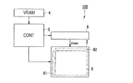
図1に示す電気泳動表示装置100は、表示体2と、コントローラー3と、VRAM(Video Random Access Memory)4と、共通電極駆動回路6とを備えている。
表示体2は、コントローラー3からの制御信号と、共通電極駆動回路6からの電圧供給を受け、画像を表示する。表示体2には、表示部5と、走査線駆動回路61と、データ線駆動回路62とが形成されている。
The
The
コントローラー3は、電気泳動表示装置100の制御部であり、表示すべき画像データをVRAM4から受け取り、表示体2を制御して画像を表示させる。具体的には、表示体2に設けられた走査線駆動回路61及びデータ線駆動回路62と共通電極駆動回路6とを制御して画像を表示させる。コントローラー3から出力される制御信号は、例えば、クロック信号、スタートパルス等のタイミング信号や画像データ、電源電圧等である。
VRAM4は、フラッシュメモリー等の記憶部(図示は省略)に記憶された画像データから、表示部5に次に表示させる1枚又は複数枚分の画像データを一時的に保存するために用いられる。
共通電極駆動回路6は、表示体2に設けられた共通電極37(対向電極;図3参照)と接続されており、任意の共通電極電位Vcomを共通電極37に供給する。
The
The VRAM 4 is used to temporarily store one or more image data to be displayed next on the
The common
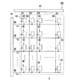
図2は、本実施形態に係る電気泳動表示装置100の概略構成を示す回路図である。
電気泳動表示装置100は、複数の画素40が配列された表示部5を有している。表示部5の周辺には、走査線駆動回路61およびデータ線駆動回路62が配置されている。走査線駆動回路61及びデータ線駆動回路62は、それぞれ上記コントローラー3と接続されている。
FIG. 2 is a circuit diagram showing a schematic configuration of the
The
表示部5には走査線駆動回路61から延びる複数の走査線66と、データ線駆動回路62から延びる複数のデータ線68とが形成されており、これらの交差位置に対応して画素40が設けられている。
A plurality of
走査線駆動回路61は、行方向に延びるm本の走査線66(Y1、Y2、Y3、…、Ym)を介して各々の画素40に接続されており、コントローラー3の制御のもと、1行目からm行目までの走査線66を順次選択し、画素40に設けられた選択トランジスタ(選択トランジスタTRa,TRb:図3参照)のオンタイミングを規定する選択信号を、選択した走査線66を介して画素40に供給する。画素40は、Y軸方向に沿ってm個、X軸方向に沿ってn個のマトリクス状に配列されている。
The scanning
本実施形態の電気泳動表示装置100において、走査線66及びデータ線68の本数は任意の自然数に設定することができる。
In the
データ線駆動回路62は、列方向に延びるn本のデータ線68(X1、X2、X3、…、Xn)を介して各々の画素40に接続されており、コントローラー3の制御のもと、画素40の各々に対応する1ビットの画像データを規定する画像信号を画素40に供給する。
なお、本実施形態では、画像データ(画素データ)「0」(白)を規定する場合にはローレベル(L)の画像信号を画素40に供給し、画像データ(画素データ)「1」(黒)を規定する場合はハイレベル(H)の画像信号を画素40に供給する。また、中間階調の画素データを規定する場合にはLからHの中間のレベルの画像信号を画素40に供給する。
The data line driving
In this embodiment, when image data (pixel data) “0” (white) is defined, a low-level (L) image signal is supplied to the
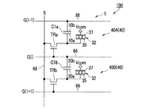
図3は、画素40A,40Bの回路構成図である。
表示部5の各画素40A,40Bには、画素スイッチング素子としての選択トランジスタTRa,TRb、画素電極35(第1電極)、電気泳動素子32、共通電極37(第2電極)及び保持容量C1a,C1bが設けられている。
選択トランジスタTRa,TRbは、それぞれN−MOS(Negative Metal Oxide Semiconductor)TFTで構成されている。
電気泳動素子32は、画素電極35と共通電極37との間で挟持されている。
保持容量C1a,C1bは後述する素子基板30(第1基板)上に形成され、誘電体膜を介して対向配置された一対の電極10a,10bによって保持容量C1aが構成され、一対の電極20a,20bによって保持容量C1bが構成されている。そして、選択トランジスタTRa,TRbを介してそれぞれ書き込まれた画像信号電圧で充電される。詳しくは後述するが、本実施形態の保持容量C1a,C1bは、隣り合う他の走査線66を利用して保持容量を形成するCs-on-gate構造とされている。
FIG. 3 is a circuit configuration diagram of the
Each
The selection transistors TRa and TRb are each composed of an N-MOS (Negative Metal Oxide Semiconductor) TFT.
The
The storage capacitors C1a and C1b are formed on an element substrate 30 (first substrate) to be described later, and a storage capacitor C1a is configured by a pair of
画素40Aの選択トランジスタTRaは、そのゲート電極にi行の走査線66が接続されるとともにソースにはデータ線68が接続されており、ドレインには保持容量C1aの一方の電極10aと画素電極35とがそれぞれ接続されている。そして、保持容量C1aの他方の電極10bはi−1行の走査線66と接続されている。
画素40Aの保持容量C1aは、当該画素40Aにおける画素電極35と、前段のi−1行の走査線66とによって容量を形成する構成とされている。
The selection transistor TRa of the
The storage capacitor C1a of the
画素40Bの選択トランジスタTRbは、そのゲート電極にi+1行の走査線66が接続されるとともにソースにはデータ線68が接続されており、ドレインには保持容量C1bの一方の電極20aと画素電極35とが接続されている。そして、保持容量C1bの他方の電極20bはi行の走査線66に接続されている。
画素40Bの保持容量C1bは、当該画素40Bにおける画素電極35と、前段のi行の走査線66とによって容量を形成する構成とされている。
The selection transistor TRb of the
The storage capacitor C1b of the
この画素回路においては、例えば、i行の走査線66が選択されると選択トランジスタTRaがオン状態となり、データ線68から選択トランジスタTRaを介して画素電極35に画像信号が入力されるとともに、保持容量C1aが充電される。i行の走査線66が非選択となると選択トランジスタTRaはオフ状態となるが、その後も保持容量C1aに蓄えられたエネルギーで画素40A内の電気泳動素子32の荷電粒子を移動させる。
また、i+1行の走査線66が選択されると選択トランジスタTRbがオン状態となり、データ線68から選択トランジスタTRbを介して画素電極35に画像信号が入力されるとともに、保持容量C1bが充電される。i+1行の走査線66が非選択となると選択トランジスタTRbはオフ状態となるが、その後も保持容量C1bに蓄えられたエネルギーで画素40B内の電気泳動素子32の荷電粒子を移動させる。
In this pixel circuit, for example, when the i-
When the i + 1-
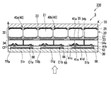
図4(a)は、表示部5における電気泳動表示装置100の部分断面図である。
電気泳動表示装置100は、素子基板30と対向基板31(第2基板)との間に、複数のマイクロカプセル20を配列してなる電気泳動素子32を挟持した構成を備えている。複数のマイクロカプセル20は、バインダー23によって固定されている。
表示部5において、素子基板30の電気泳動素子32側には複数の画素電極35が配列形成されており、電気泳動素子32は接着剤層33を介して画素電極35と接着されている。
FIG. 4A is a partial cross-sectional view of the
The
In the
素子基板30は、ガラスやプラスチック等からなる基板であり、画像表示側に配置されるため透明基板とされる。素子基板30の表面には、着色層51r、51g、51b及び保護層52を備えたカラーフィルターCFが形成されている。カラーフィルターCF上には、走査線66、データ線68、選択トランジスタTRa,TRb等を含む回路層34が設けられており、この回路層34の最表層に複数の画素電極35が配列形成されている。
画素電極35は、MgAg、ITO、IZO(インジウム・亜鉛酸化物)などから形成された透明電極である。図示は省略しているが、画素電極35と素子基板30との間には、図3及び図4に示した走査線66、データ線68、選択トランジスタTRa,TRbなどが形成されている。
The
The
一方、対向基板31はガラスやプラスチック等からなる基板であり、画像表示面とは反対側に配置されるため透明なものでなくてもよい。対向基板31の電気泳動素子32側には複数の画素電極35と対向する平面形状の共通電極37が形成されており、共通電極37上に電気泳動素子32が設けられている。本実施形態における共通電極37は光反射性を有したいわゆる反射電極である。共通電極37には、Cr、Mo、Mo合金、Al、Al合金、Ta、Ti、Ag合金、Ni合金などの金属材料を用いることができる。なお、反射電極の材料としては、金属に限らず、金属光沢を有する導電性プラスチックであってもよい。共通電極37を反射電極としておくことで、素子基板30側から入射した光のうち電気泳動粒子にて反射されずに、電気泳動粒子同士の間やマイクロカプセル20同士の間のすき間を通り抜けた光を共通電極37にて反射させることができる。これにより、光の利用効率が向上し、表示部5における輝度を高めることが可能となる。
On the other hand, the
なお、電気泳動素子32は、あらかじめ対向基板31側に形成され、接着剤層33までを含めた電気泳動シートとして取り扱われるのが一般的である。製造工程において、電気泳動シートは接着剤層33の表面に保護用の剥離シートが貼り付けられた状態で取り扱われる。そして、別途製造された素子基板30(画素電極35や各種回路などが形成されている)に対して、剥離シートを剥がした当該電気泳動シートを貼り付けることによって、表示部5を形成する。このため、接着剤層33は画素電極35側のみに存在することになる。
In general, the
図4(b)は、マイクロカプセル20の模式断面図である。
マイクロカプセル20は、例えば50μm程度の粒径を有しており、内部に分散媒21と、複数の白色粒子(電気泳動粒子)27と、複数の黒色粒子(電気泳動粒子)26とを封入した球状体である。マイクロカプセル20は、図4(a)に示すように共通電極37と画素電極35とで挟持され、1つの画素40内に1つ又は複数のマイクロカプセル20が配置される。
FIG. 4B is a schematic cross-sectional view of the
The
マイクロカプセル20の外殻部(壁膜)は、ポリメタクリル酸メチル、ポリメタクリル酸エチルなどのアクリル樹脂、ユリア樹脂、アラビアゴムなどの透光性を持つ高分子樹脂などを用いて形成される。
分散媒21は、白色粒子27と黒色粒子26とをマイクロカプセル20内に分散させる液体である。分散媒21としては、水、アルコール系溶媒(メタノール、エタノール、イソプロパノール、ブタノール、オクタノール、メチルセルソルブなど)、エステル類(酢酸エチル、酢酸ブチルなど)、ケトン類(アセトン、メチルエチルケトン、メチルイソブチルケトンなど)、脂肪族炭化水素(ぺンタン、ヘキサン、オクタンなど)、脂環式炭化水素(シクロへキサン、メチルシクロへキサンなど)、芳香族炭化水素(ベンゼン、トルエン、長鎖アルキル基を有するベンゼン類(キシレン、ヘキシルベンゼン、ヘブチルベンゼン、オクチルベンゼン、ノニルベンゼン、デシルベンゼン、ウンデシルベンゼン、ドデシルベンゼン、トリデシルベンゼン、テトラデシルベンゼンなど))、ハロゲン化炭化水素(塩化メチレン、クロロホルム、四塩化炭素、1,2−ジクロロエタンなど)、カルボン酸塩などを例示することができ、その他の油類であってもよい。これらの物質は単独又は混合物として用いることができ、さらに界面活性剤などを配合してもよい。
The outer shell (wall film) of the
The
白色粒子27は、例えば、二酸化チタン、亜鉛華、三酸化アンチモン等の白色顔料からなる粒子(高分子あるいはコロイド)であり、例えば負に帯電されて用いられる。黒色粒子26は、例えば、アニリンブラック、カーボンブラック等の黒色顔料からなる粒子(高分子あるいはコロイド)であり、例えば正に帯電されて用いられる。
これらの顔料には、必要に応じ、電解質、界面活性剤、金属石鹸、樹脂、ゴム、油、ワニス、コンパウンドなどの粒子からなる荷電制御剤、チタン系カップリング剤、アルミニウム系カップリング剤、シラン系カップリング剤等の分散剤、潤滑剤、安定化剤などを添加することができる。
また、黒色粒子26及び白色粒子27に代えて、例えば赤色、緑色、青色などの顔料を用いてもよい。かかる構成によれば、表示部5に赤色、緑色、青色などを表示することができる。
The
These pigments include electrolytes, surfactants, metal soaps, resins, rubbers, oils, varnishes, compound charge control agents, titanium-based coupling agents, aluminum-based coupling agents, silanes as necessary. A dispersant such as a system coupling agent, a lubricant, a stabilizer, and the like can be added.
Further, instead of the
ここで図5(a)は、1つの画素40における素子基板30の平面図であり、図5(b)は、図5(a)のA−A’線に沿う位置における断面図である。
図5(a)に示すように、選択トランジスタTRa,TRbは、平面視略矩形状の半導体層41aと、データ線68から延出されたソース電極41cと、半導体層41aと画素電極35とを接続するドレイン電極41dと、走査線66から延出されたゲート電極41eとをそれぞれ有する。また、各画素40A,40Bにおいて、画素電極35と走査線66とが重なる領域にそれぞれ保持容量C1a,C1bが形成されている。
Here, FIG. 5A is a plan view of the
As shown in FIG. 5A, the selection transistors TRa and TRb include a
近年の小型な表示パネルは高精細化が進んできており、それに伴い電極及び配線間の寄生容量によるクロストークが発生しやすいので、大きな保持容量が要求されていた。しかしながら、高精細化に伴い画素電極35以外のデータ線68ないし走査線66の占める割合も増えているため、保持容量の増大化に伴う画素の開口率低下の問題点は顕著に現れてくる。一画素内における保持容量の形成面積が大きいと画素の開口率が低下して十分な表示コントラストを得ることができなくなってしまうため、素子基板30側からの観測は困難であった。
In recent years, small display panels have been improved in definition, and accordingly, crosstalk due to parasitic capacitance between electrodes and wiring tends to occur, so that a large storage capacitor has been required. However, since the ratio of the data lines 68 to the
そこで、本実施形態では、画素電極35の形成面積に対して保持容量の形成面積を小さくすることで、保持容量が画素領域を占める割合を少なくするとともに、走査線66の一部を延在形成して画素電極35に重畳配置した、いわゆるCs-on-gate構造とすることで回路素子が存在しない光透過部42の面積を大きくしている。これにより、画素40内の開口率が高まり素子基板30の裏面側からの光を十分に透過させることができる。
Therefore, in the present embodiment, by reducing the formation area of the storage capacitor with respect to the formation area of the
図5(b)に示す断面構造を見ると、素子基板30上に、AlやAl合金からなるゲート電極41e(走査線66)が形成されており、ゲート電極41eを覆ってシリコン酸化物やシリコン窒化物からなるゲート絶縁膜41bが形成されている。ゲート絶縁膜41bの厚みは約300nmである。ゲート絶縁膜41bを介してゲート電極41eと対向する領域にアモルファスシリコンやポリシリコンからなる半導体層41aが形成されている。半導体層41aに一部乗り上げるようにして、AlやAl合金からなるソース電極41cとドレイン電極41dとが形成されている。ソース電極41c(データ線68)、ドレイン電極41d、半導体層41a、ゲート絶縁膜41bを覆ってシリコン酸化物やシリコン窒化物からなる層間絶縁膜34aが形成されている。層間絶縁膜34a上に画素電極35が形成されている。層間絶縁膜34aを貫通しドレイン電極41dに達するコンタクトホール34bを介して画素電極35とドレイン電極41dとが接続されている。このようにして、選択トランジスタTRa,TRbが構成されている。
5B, the
ここで、ゲート電極41eや画素電極35、各種配線の厚みは約100nmから300nmである。また、ゲート電極41eや各種配線が電気泳動素子32に及ぼす電気的影響を低減するために、これらはできるだけ細い線幅とすることが好ましい。具体的には、約4μm以下の線幅が好適である。
Here, the thicknesses of the
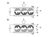
図6は、電気泳動素子の動作説明図である。図6(a)は、画素40を白表示する場合、図6(b)は、画素40を黒表示する場合をそれぞれ示している。
図6(a)に示す白表示の場合には、共通電極37が相対的に高電位、画素電極35が相対的に低電位に保持される。これにより、負に帯電した白色粒子27が共通電極37に引き寄せられる一方、正に帯電した黒色粒子26が画素電極35に引き寄せられる。その結果、表示面側となる共通電極37側からこの画素を見ると、白色(W)が認識される。
図6(b)に示す黒表示の場合、共通電極37が相対的に低電位、画素電極35が相対的に高電位に保持される。これにより、正に帯電した黒色粒子26が共通電極37に引き寄せられる一方、負に帯電した白色粒子27が画素電極35に引き寄せられる。その結果、共通電極37側からこの画素を見ると黒色(B)が認識される。
FIG. 6 is an operation explanatory diagram of the electrophoretic element. FIG. 6A shows a case where the
In the case of white display shown in FIG. 6A, the
In the case of black display shown in FIG. 6B, the
なお、図6は、黒粒子が正に、白粒子が負に帯電している場合の動作説明図であるが、必要に応じて、黒粒子を負に、白粒子を正に帯電させてもよい。この場合、上記と同様に電位を供給すると、白表示と黒表示とを反転した表示が得られる。 FIG. 6 is an operation explanatory diagram when black particles are positively charged and white particles are negatively charged. However, if necessary, black particles can be negatively charged and white particles can be positively charged. Good. In this case, when a potential is supplied in the same manner as described above, a display in which white display and black display are reversed can be obtained.
以上のように構成された電気泳動表示装置100においては、昼間や室内等の明るい場所では外光が素子基板30側から入射し、電気泳動素子32を透過した後に共通電極37にて反射され、再び電気泳動素子32を透過して放出されるので、素子基板30側から見ると反射型表示が視認される。
実際には、素子基板30側から入射した光のほとんどが電気泳動粒子にて反射されることになるが、これら粒子間やマイクロカプセル20の間のすき間を透過した光が共通電極37にて反射されることになる。このように、粒子間やマイクロカプセル20の間のすき間を透過した光を有効に利用することが可能となる。
In the
Actually, most of the light incident from the
本実施形態によれば、Cs on gate構造にして各画素40の開口率を高めるとともに共通電極37を反射電極とすることで、電気泳動素子32に入射する光の透過率及び反射率を向上させている。共通電極37を反射電極としておくことで、素子基板30側から入射した光のうち電気泳動粒子にて反射されずに、電気泳動粒子同士の間やマイクロカプセル20同士の間のすき間を通り抜けた光を共通電極37にて反射させることができる。
According to the present embodiment, the Cs on gate structure is used to increase the aperture ratio of each
これにより、素子基板30側から放出される光の量が多くなり、素子基板30側の輝度が上昇して視認性が高められ、画像のコントラストが向上するという効果が得られる。このように、素子基板30側から表示画像を観測する反射型表示装置において、トランジスタや配線等によって光透過率及び光反射率が低下するのを防止して、全ての画像がユーザーによって視認されることを可能としている。さらに、自然光などの環境光を効率的に利用して光の反射率を向上させることで、低消費電力で表示用の光を確保することができる。
Thereby, the amount of light emitted from the
また、本実施形態では、素子基板30と回路層34との間にカラーフィルターCFが配置されていることから、カラーフィルターCFと画素電極35との距離が近づくので、素子基板30側から観測した場合に、諧調の境界がぼやけたりすることがなく、カラーフィルターCFの色の境界と、電気泳動素子32の色の境界あるいは画像の輪郭とのずれが生じることが防止され、モアレ発生等をなくすことが可能となる。これにより、表示画像のコントラストが向上し、視認性が高められる。
In the present embodiment, since the color filter CF is disposed between the
[第2実施形態]
次に、本発明の第2実施形態における電気泳動表示装置200について述べる。図7に本実施形態の電気泳動表示装置200の断面図を示す。本実施形態の電気泳動表示装置200は、第1実施形態の対向基板の構成において異なる。
[Second Embodiment]
Next, an
本実施形態の電気泳動表示装置200は、対向基板が金属基板55となっている。金属基板55としては、Cr、Mo、Mo合金、Al、Al合金、Ta、Ti、Ag合金、Ni合金などの金属材料を用いることができる。金属基板55は電気泳動表示装置200の最外層に位置する部材のため、剛性を有していることが好ましい。素子基板30と貼り合わされる前の金属基板55の内側には共通電極は形成されず、電気泳動素子32としての電気泳動シートが直接貼り合わされて製造される。すなわち、本実施形態における金属基板55は共通電極の機能も兼ねており、不図示の配線を介して接続された共通電極駆動回路6からの電圧供給を受ける構成とされている。
そして、共通電極駆動回路6からの任意の共通電極電位Vcomが供給されることで、金属基板55と画素電極35との間に電位差が生じ、この電位差によって電気泳動素子32が駆動して表示部5に画像が表示される。
In the
Then, by supplying an arbitrary common electrode potential Vcom from the common
本実施形態の電気泳動表示装置200によれば、対向基板を金属基板55とすることで共通電極として機能させることができ、これに伴い共通電極の形成工程を削減できて製造が容易になる。また、金属基板55とすることで基板自体が光反射性を有する部材となり、素子基板30側から入射した光のうち電気泳動粒子26,27間やマイクロカプセル20の間の隙間を通って金属基板55へ入射した光を素子基板30側へ反射させることが可能となる。これにより、光の利用効率が向上する。よって、素子基板30側の輝度が上昇して視認性が高められ、画像のコントラストが向上するという上記実施形態同様の効果が得られる。
According to the
[第3実施形態]
次に、本発明の第3実施形態における電気泳動表示装置300について述べる。図8に本実施形態の電気泳動表示装置300の部分拡大断面図を示す。本実施形態の電気泳動表示装置300は、先の実施形態の対向基板の構成において異なる。なお、図8では選択トランジスタTRa,TRb等の図示を省略してある。
[Third Embodiment]
Next, an
本実施形態の電気泳動表示装置300は、基板面から順に共通電極37と絶縁層74とが順に形成された対向基板31と、この対向基板31と電気泳動素子を介して対向配置される素子基板30とを備えてなり、対向基板31と素子基板30との間に配置された隔壁72によって電気泳動素子3が複数の領域に分割されている。
隔壁72は、電気泳動表示装置300の厚さ方向に一定の高さを有して形成された、複数の封止空間を区画(分割)する平面視格子状の隔壁であって、光反射性を有する材料から構成されている。隔壁72としては、例えば金属光沢を有する導電性プラスチックなどを用いることができる。本実施形態の隔壁72は、絶縁層74により共通電極37と電気的に分離しているため、反射電極の材料として挙げた上記金属材料を用いて形成してもよい。なお、本実施形態の共通電極37も第1実施形態と同様に光反射性を有した電極となっている。
共通電極37の表面が絶縁層74で覆われた構成としておくことで分散媒21から共通電極37を保護することができるので、電極の劣化を防止できる。
The
The
By setting the surface of the
このような構成により、この枠状の隔壁72の内側の空間がマトリックス状の複数の封止空間71に分割され、対向基板31と素子基板30との間で各封止空間71がそれぞれ気密的に封止されている。素子基板30の内側(対向基板31と対向する側)の最表層に、複数の画素電極35を覆うようにして絶縁層73を形成しておくことで、導電性を有する隔壁72の場合に画素電極35と隔壁72との絶縁性が確保されるとともに分散媒21から電極を保護することができる。そして、隔壁72によって形成される各封止空間71内には、電気泳動素子32を構成する分散媒21と、複数の白色粒子27と、複数の黒色粒子26とが封入されており、この封止空間71内にて各粒子26,27が移動するようになっている。
With such a configuration, the space inside the frame-shaped
本実施形態の構成によれば、光反射性を有する隔壁72を設けることにより、素子基板30側から入射した光が共通電極37だけでなく隔壁72においても反射されることになるため、各画素40の輝度が向上し、より良好な視認性を得ることが可能となる。
According to the configuration of the present embodiment, by providing the
以上、添付図面を参照しながら本発明に係る好適な実施形態について説明したが、本発明は係る例に限定されないことは言うまでもない。当業者であれば、特許請求の範囲に記載された技術的思想の範疇内において、各種の変更例または修正例に想到し得ることは明らかであり、それらについても当然に本発明の技術的範囲に属するものと了解される。 As described above, the preferred embodiments according to the present invention have been described with reference to the accompanying drawings, but the present invention is not limited to the examples. It is obvious for those skilled in the art that various changes or modifications can be conceived within the scope of the technical idea described in the claims. It is understood that it belongs to.
例えば、電気泳動素子32を構成するマイクロカプセル20の外殻部(壁膜)が光反射性を有していてもよい。この場合、例えば半球面上に反射膜を形成しておき、各マイクロカプセル20の反射膜を対向基板31側に揃えた状態で配置させる構成が考えられる。これにより、素子基板30から入射した光がマイクロカプセル20の壁膜の透明側から入射し、反射膜にて反射されて外部へ放射されることになる。反射膜により十分な反射光が得られるのであれば、共通電極や対向基板に反射性を有するものを用いずに従来のものを採用してもよいし、光反射性を有する共通電極37(図4)あるいは対向基板(金属基板55:図7)と併用しても構わない。
For example, the outer shell (wall film) of the
また、複数のマイクロカプセル20を固定しているバインダー23が光反射性を有していてもよい。これにより、共通電極37に入射しない光を反射させることができる。つまり、マイクロカプセルを透過した光は共通電極37にて反射され、それ以外の光はバインダー23によって反射されることになる。
このような構成とすることで、環境光を有効に活用することができ、表示部5の輝度が向上してより良好な視認性を得ることができる。
Further, the
By setting it as such a structure, environmental light can be utilized effectively and the brightness | luminance of the
また、先の実施形態では、選択トランジスタTRa,TRbとしてアモルファスシリコンTFTを使用した例について述べたが、チャネルエッチタイプのアモルファスシリコンTFT、HTPS(高温ポリシリコン)TFT、LTPS(低温ポリシリコン)TFT、酸化物TFT、有機TFTを用いてもよい。 In the previous embodiment, an example in which amorphous silicon TFTs are used as the selection transistors TRa and TRb has been described. However, channel etch type amorphous silicon TFTs, HTPS (high temperature polysilicon) TFTs, LTPS (low temperature polysilicon) TFTs, An oxide TFT or an organic TFT may be used.
(電子機器)
次に、上記実施形態の電気泳動表示装置100、200、300を、電子機器に適用した場合について説明する。
図9は、腕時計1000の正面図である。腕時計1000は、時計ケース1002と、時計ケース1002に連結された一対のバンド1003とを備えている。
時計ケース1002の正面には、上記各実施形態の電気泳動表示装置からなる表示部1005と、秒針1021と、分針1022と、時針1023とが設けられている。時計ケース1002の側面には、操作子としての竜頭1010と操作ボタン1011とが設けられている。竜頭1010は、ケース内部に設けられる巻真(図示は省略)に連結されており、巻真と一体となって多段階(例えば2段階)で押し引き自在、かつ、回転自在に設けられている。表示部1005では、背景となる画像、日付や時間などの文字列、あるいは秒針、分針、時針などを表示することができる。
(Electronics)
Next, the case where the
FIG. 9 is a front view of the
On the front surface of the
図10は電子ペーパー1100の構成を示す斜視図である。電子ペーパー1100は、上記実施形態の電気泳動表示装置を表示領域1101に備えている。電子ペーパー1100は可撓性を有し、従来の紙と同様の質感及び柔軟性を有する書き換え可能なシートからなる本体1102を備えて構成されている。
FIG. 10 is a perspective view illustrating a configuration of the
図11は、電子ノート1200の構成を示す斜視図である。電子ノート1200は、上記の電子ペーパー1100が複数枚束ねられ、カバー1201に挟まれているものである。カバー1201は、例えば外部の装置から送られる表示データを入力する図示は省略の表示データ入力手段を備える。これにより、その表示データに応じて、電子ペーパーが束ねられた状態のまま、表示内容の変更や更新を行うことができる。
FIG. 11 is a perspective view showing the configuration of the
以上の腕時計1000、電子ペーパー1100、及び電子ノート1200によれば、本発明に係る電気泳動表示装置が採用されているので、動作信頼性に優れ、表示品質の高い表示部を備えた電子機器となる。
According to the
なお、上記の電子機器は、本発明に係る電子機器を例示するものであって、本発明の技術範囲を限定するものではない。例えば、携帯電話、携帯用オーディオ機器などの電子機器の表示部にも、本発明に係る電気泳動表示装置は好適に用いることができる。 In addition, said electronic device illustrates the electronic device which concerns on this invention, Comprising: The technical scope of this invention is not limited. For example, the electrophoretic display device according to the present invention can be suitably used for a display portion of an electronic device such as a mobile phone or a portable audio device.
100,200,300…電気泳動表示装置、5…表示部、20…マイクロカプセル、30…素子基板(第1基盤)、31…対向基板(第2基板)、32…電気泳動粒子、34…回路層、35…画素電極(第1電極)、37…共通電極(第2電極)、40…画素、66…走査線、68…データ線、C1a,C1b…保持容量、TRa,TRb…選択トランジスタ、CF…カラーフィルター、1100…電子ペーパー(電子機器)、1200…電子ノート(電子機器)
DESCRIPTION OF SYMBOLS 100,200,300 ... Electrophoretic display apparatus, 5 ... Display part, 20 ... Microcapsule, 30 ... Element substrate (1st board | substrate), 31 ... Opposite substrate (2nd substrate), 32 ... Electrophoretic particle, 34 ...
Claims (7)
前記第1基板に対向して配置された第2基板と、
前記第1基板と前記第2基板との間に配置された電気泳動素子と、
前記第1基板の前記電気泳動素子側に形成された複数の第1電極と、
前記第2基板の前記電気泳動素子側に、前記複数の第1電極と対向するように形成された第2電極と、を有する電気泳動表示装置であって、
前記第2電極が光反射性を有することを特徴とする電気泳動表示装置。 A first substrate;
A second substrate disposed opposite the first substrate;
An electrophoretic element disposed between the first substrate and the second substrate;
A plurality of first electrodes formed on the electrophoretic element side of the first substrate;
An electrophoretic display device having, on the electrophoretic element side of the second substrate, a second electrode formed to face the plurality of first electrodes,
The electrophoretic display device, wherein the second electrode has light reflectivity.
前記複数の第1電極の各々に接続された、一対の電極を有する保持容量と、を有し、
前記走査線が前記一対の電極の一方の電極となっていることを特徴とする請求項1から3のいずれか一項に記載の電気泳動表示装置。 A plurality of scanning lines each connected to at least one of the plurality of first electrodes via a select transistor;
A storage capacitor having a pair of electrodes connected to each of the plurality of first electrodes,
The electrophoretic display device according to claim 1, wherein the scanning line is one electrode of the pair of electrodes.
前記第1基板と前記第2基板との間で前記複数のマイクロカプセルを固定しているバインダーが光反射性を有していることを特徴とする請求項1から4のいずれか一項に記載の電気泳動表示装置。 The electrophoretic element has a plurality of microcapsules containing a plurality of electrophoretic particles,
5. The binder according to claim 1, wherein a binder that fixes the plurality of microcapsules between the first substrate and the second substrate has light reflectivity. 6. Electrophoretic display device.
前記隔壁と、当該隔壁によって区画形成される空間内に封入された電気泳動粒子および分散媒とにより、前記電気泳動素子が構成されていることを特徴とする請求項1から5のいずれか一項に記載の電気泳動表示装置。 A partition wall having light reflectivity is provided between the first substrate and the second substrate;
6. The electrophoretic element is constituted by the partition, and electrophoretic particles and a dispersion medium sealed in a space defined by the partition. 6. The electrophoretic display device described in 1.
Priority Applications (2)
| Application Number | Priority Date | Filing Date | Title |
|---|---|---|---|
| JP2010005006A JP2011145391A (en) | 2010-01-13 | 2010-01-13 | Electrophoretic display device and electronic equipment |
| US12/973,157 US20110170169A1 (en) | 2010-01-13 | 2010-12-20 | Electrophoretic display device and electronic apparatus |
Applications Claiming Priority (1)
| Application Number | Priority Date | Filing Date | Title |
|---|---|---|---|
| JP2010005006A JP2011145391A (en) | 2010-01-13 | 2010-01-13 | Electrophoretic display device and electronic equipment |
Publications (2)
| Publication Number | Publication Date |
|---|---|
| JP2011145391A true JP2011145391A (en) | 2011-07-28 |
| JP2011145391A5 JP2011145391A5 (en) | 2013-02-28 |
Family
ID=44258338
Family Applications (1)
| Application Number | Title | Priority Date | Filing Date |
|---|---|---|---|
| JP2010005006A Withdrawn JP2011145391A (en) | 2010-01-13 | 2010-01-13 | Electrophoretic display device and electronic equipment |
Country Status (2)
| Country | Link |
|---|---|
| US (1) | US20110170169A1 (en) |
| JP (1) | JP2011145391A (en) |
Cited By (2)
| Publication number | Priority date | Publication date | Assignee | Title |
|---|---|---|---|---|
| WO2014030338A1 (en) * | 2012-08-22 | 2014-02-27 | 凸版印刷株式会社 | Electrophoretic display substrate, method for inspecting same, and electrophoretic display device |
| JP2016009090A (en) * | 2014-06-24 | 2016-01-18 | セイコーエプソン株式会社 | Display device and manufacturing method of display device |
Families Citing this family (6)
| Publication number | Priority date | Publication date | Assignee | Title |
|---|---|---|---|---|
| CN102645811B (en) | 2011-11-23 | 2014-07-02 | 京东方科技集团股份有限公司 | Electronic-paper active substrate and manufacturing method thereof and electronic-paper display screen |
| KR101980758B1 (en) * | 2012-12-14 | 2019-08-28 | 엘지디스플레이 주식회사 | Organic light emitting diode display device |
| JP6260309B2 (en) * | 2014-01-31 | 2018-01-17 | セイコーエプソン株式会社 | Display device |
| KR20160086525A (en) * | 2015-01-09 | 2016-07-20 | 삼성디스플레이 주식회사 | Liquid crystal display device |
| TWI554816B (en) * | 2015-07-31 | 2016-10-21 | 元太科技工業股份有限公司 | Reflective display device |
| JP2020187180A (en) * | 2019-05-10 | 2020-11-19 | 株式会社ジャパンディスプレイ | Display device |
Citations (10)
| Publication number | Priority date | Publication date | Assignee | Title |
|---|---|---|---|---|
| JP2001242806A (en) * | 1999-12-20 | 2001-09-07 | Ricoh Co Ltd | Display medium and writing device |
| JP2007034037A (en) * | 2005-07-28 | 2007-02-08 | Canon Inc | Particle migration type display device |
| JP2007041169A (en) * | 2005-08-01 | 2007-02-15 | Nec Lcd Technologies Ltd | Color electronic paper display device |
| JP2008084642A (en) * | 2006-09-27 | 2008-04-10 | Seiko Epson Corp | Electronic device, organic electroluminescent device, and organic thin film semiconductor device |
| JP2008107752A (en) * | 2006-09-28 | 2008-05-08 | Bridgestone Corp | Panel for information display |
| JP2008134600A (en) * | 2006-10-25 | 2008-06-12 | Seiko Epson Corp | Electrooptic device and electronic apparatus |
| JP2008171011A (en) * | 2001-02-20 | 2008-07-24 | Sharp Corp | Display |
| US20080218068A1 (en) * | 2007-03-05 | 2008-09-11 | Cok Ronald S | Patterned inorganic led device |
| US20090262270A1 (en) * | 2008-04-16 | 2009-10-22 | Samsung Electronics Co., Ltd. | Liquid crystal display device |
| JP2010002573A (en) * | 2008-06-19 | 2010-01-07 | Murakami Corp | Method for changing reflectivity reversibly, element therefor, method of manufacturing element, and transmittance variable element and reflectivity variable mirror |
Family Cites Families (1)
| Publication number | Priority date | Publication date | Assignee | Title |
|---|---|---|---|---|
| JP4265149B2 (en) * | 2001-07-25 | 2009-05-20 | セイコーエプソン株式会社 | Electro-optical device and method for manufacturing electro-optical device |
-
2010
- 2010-01-13 JP JP2010005006A patent/JP2011145391A/en not_active Withdrawn
- 2010-12-20 US US12/973,157 patent/US20110170169A1/en not_active Abandoned
Patent Citations (10)
| Publication number | Priority date | Publication date | Assignee | Title |
|---|---|---|---|---|
| JP2001242806A (en) * | 1999-12-20 | 2001-09-07 | Ricoh Co Ltd | Display medium and writing device |
| JP2008171011A (en) * | 2001-02-20 | 2008-07-24 | Sharp Corp | Display |
| JP2007034037A (en) * | 2005-07-28 | 2007-02-08 | Canon Inc | Particle migration type display device |
| JP2007041169A (en) * | 2005-08-01 | 2007-02-15 | Nec Lcd Technologies Ltd | Color electronic paper display device |
| JP2008084642A (en) * | 2006-09-27 | 2008-04-10 | Seiko Epson Corp | Electronic device, organic electroluminescent device, and organic thin film semiconductor device |
| JP2008107752A (en) * | 2006-09-28 | 2008-05-08 | Bridgestone Corp | Panel for information display |
| JP2008134600A (en) * | 2006-10-25 | 2008-06-12 | Seiko Epson Corp | Electrooptic device and electronic apparatus |
| US20080218068A1 (en) * | 2007-03-05 | 2008-09-11 | Cok Ronald S | Patterned inorganic led device |
| US20090262270A1 (en) * | 2008-04-16 | 2009-10-22 | Samsung Electronics Co., Ltd. | Liquid crystal display device |
| JP2010002573A (en) * | 2008-06-19 | 2010-01-07 | Murakami Corp | Method for changing reflectivity reversibly, element therefor, method of manufacturing element, and transmittance variable element and reflectivity variable mirror |
Cited By (5)
| Publication number | Priority date | Publication date | Assignee | Title |
|---|---|---|---|---|
| WO2014030338A1 (en) * | 2012-08-22 | 2014-02-27 | 凸版印刷株式会社 | Electrophoretic display substrate, method for inspecting same, and electrophoretic display device |
| JP5500329B1 (en) * | 2012-08-22 | 2014-05-21 | 凸版印刷株式会社 | Electrophoretic display substrate, inspection method thereof, and electrophoretic display device |
| JP2014112263A (en) * | 2012-08-22 | 2014-06-19 | Toppan Printing Co Ltd | Electrophoretic display substrate, electrophoretic display device, electronic paper, method for manufacturing electrophoretic display device, and method for manufacturing electronic paper |
| US9874798B2 (en) | 2012-08-22 | 2018-01-23 | Toppan Printing Co., Ltd. | Electrophoretic display substrate, method of inspecting same, and electrophoretic display device |
| JP2016009090A (en) * | 2014-06-24 | 2016-01-18 | セイコーエプソン株式会社 | Display device and manufacturing method of display device |
Also Published As
| Publication number | Publication date |
|---|---|
| US20110170169A1 (en) | 2011-07-14 |
Similar Documents
| Publication | Publication Date | Title |
|---|---|---|
| JP2011145391A (en) | Electrophoretic display device and electronic equipment | |
| JP5200700B2 (en) | Electrophoretic display device and electronic apparatus | |
| JP2011221097A (en) | Substrate for electrophoretic display device, electrophoretic display device and electronic apparatus | |
| JP2011145344A (en) | Electric optical apparatus, driving method thereof and electronic device | |
| JP2011221098A (en) | Substrate for electro-optic device, electro-optic device and electronic apparatus | |
| JP2010204629A (en) | Method of driving electrophoretic display apparatus, electrophoretic display apparatus, and electronic device | |
| JP5370087B2 (en) | Electrophoretic display device driving method, electrophoretic display device, and electronic apparatus | |
| JP2011099897A (en) | Driving method of electrophoretic display device, the electrophoretic display device, and electronic apparatus | |
| JP2009175409A (en) | Electrophoretic display device driving method, electrophoretic display device and electronic equipment | |
| JP2011123216A (en) | Method of driving electrophoretic display device, electrophoretic display device and electronic equipment | |
| JP2011150010A (en) | Electrooptical device, method of driving the same, and electronic apparatus | |
| JP5581677B2 (en) | Electrophoretic display device and electronic apparatus | |
| JP5568975B2 (en) | Electrophoretic display device, driving method of electrophoretic display device, and electronic apparatus | |
| JP2011164196A (en) | Electrooptical device substrate, electrooptical device, and electronic equipment | |
| JP5375007B2 (en) | Matrix device drive circuit, matrix device, image display device, electrophoretic display device, and electronic apparatus | |
| JP2011145389A (en) | Electro-optical device, method of manufacturing the same, substrate for electro-optical device, and electronic apparatus | |
| JP2010181618A (en) | Method of driving electrophoretic display device, electrophoretic display device, and electronic apparatus | |
| JP5359840B2 (en) | Electrophoretic display device driving method, electrophoretic display device, and electronic apparatus | |
| JP2011150009A (en) | Electrooptical device, method of driving the same, and electronic apparatus | |
| JP2011221099A (en) | Substrate for electro-optic device, electro-optic device and electronic apparatus | |
| JP5499638B2 (en) | Electrophoretic display device, driving method thereof, and electronic apparatus | |
| US20100085343A1 (en) | Electrophoretic display, electronic apparatus, and method for driving electrophoretic display | |
| JP2011145390A (en) | Electrophoretic display device and electronic equipment | |
| JP2011095564A (en) | Electrophoretic display device, driving method of the same, and electronic apparatus | |
| JP5262539B2 (en) | Electrophoretic display device and electronic apparatus |
Legal Events
| Date | Code | Title | Description |
|---|---|---|---|
| RD04 | Notification of resignation of power of attorney |
Free format text: JAPANESE INTERMEDIATE CODE: A7424 Effective date: 20120201 |
|
| A521 | Request for written amendment filed |
Free format text: JAPANESE INTERMEDIATE CODE: A523 Effective date: 20130110 |
|
| A621 | Written request for application examination |
Free format text: JAPANESE INTERMEDIATE CODE: A621 Effective date: 20130110 |
|
| A131 | Notification of reasons for refusal |
Free format text: JAPANESE INTERMEDIATE CODE: A131 Effective date: 20130709 |
|
| A977 | Report on retrieval |
Free format text: JAPANESE INTERMEDIATE CODE: A971007 Effective date: 20130710 |
|
| A761 | Written withdrawal of application |
Free format text: JAPANESE INTERMEDIATE CODE: A761 Effective date: 20130906 |