JP2011101266A - Semiconductor device and information processing system - Google Patents
Semiconductor device and information processing system Download PDFInfo
- Publication number
- JP2011101266A JP2011101266A JP2009255568A JP2009255568A JP2011101266A JP 2011101266 A JP2011101266 A JP 2011101266A JP 2009255568 A JP2009255568 A JP 2009255568A JP 2009255568 A JP2009255568 A JP 2009255568A JP 2011101266 A JP2011101266 A JP 2011101266A
- Authority
- JP
- Japan
- Prior art keywords
- voltage
- output
- power supply
- output driver
- output signal
- Prior art date
- Legal status (The legal status is an assumption and is not a legal conclusion. Google has not performed a legal analysis and makes no representation as to the accuracy of the status listed.)
- Withdrawn
Links
Images
Classifications
-
- H—ELECTRICITY
- H03—ELECTRONIC CIRCUITRY
- H03K—PULSE TECHNIQUE
- H03K19/00—Logic circuits, i.e. having at least two inputs acting on one output; Inverting circuits
- H03K19/003—Modifications for increasing the reliability for protection
- H03K19/00369—Modifications for compensating variations of temperature, supply voltage or other physical parameters
- H03K19/00384—Modifications for compensating variations of temperature, supply voltage or other physical parameters in field effect transistor circuits
-
- H—ELECTRICITY
- H03—ELECTRONIC CIRCUITRY
- H03K—PULSE TECHNIQUE
- H03K19/00—Logic circuits, i.e. having at least two inputs acting on one output; Inverting circuits
- H03K19/003—Modifications for increasing the reliability for protection
- H03K19/00346—Modifications for eliminating interference or parasitic voltages or currents
- H03K19/00361—Modifications for eliminating interference or parasitic voltages or currents in field effect transistor circuits
Landscapes
- Physics & Mathematics (AREA)
- Engineering & Computer Science (AREA)
- Computer Hardware Design (AREA)
- Computing Systems (AREA)
- General Engineering & Computer Science (AREA)
- Mathematical Physics (AREA)
- Logic Circuits (AREA)
- Dram (AREA)
- Semiconductor Integrated Circuits (AREA)
Abstract
Description
本発明は半導体装置及び情報処理システムに関し、特に、電源電圧が可変である半導体装置及びこれを備える情報処理システムに関する。 The present invention relates to a semiconductor device and an information processing system, and more particularly to a semiconductor device having a variable power supply voltage and an information processing system including the same.
DRAM(Dynamic Random Access Memory)などの半導体装置においては、標準化のため電源電圧などが規格によって厳密に定められている。例えば、DDR(Double Data Rate)3型のSDRAM(Synchronous DRAM)では、電源電圧が1.5Vに規定されている(非特許文献1)。
In a semiconductor device such as a DRAM (Dynamic Random Access Memory), the power supply voltage and the like are strictly determined by the standard for standardization. For example, in a DDR (Double Data Rate)
他方、近年においては低消費電力化の要求が非常に強いため、電源電圧をより低電圧化する試みが数多くなされている。しかしながら、電源電圧を変化させると、出力ドライバからの出力信号の波形も変化することから、そのままでは信号の送受信を正しく行うことができない。このため、出力ドライバや入力レシーバに対する種々の調整が必要となる。一般的には、電源電圧を低下させる場合、出力ドライバのスルーレートについては電源電圧を低下させる前のスルーレートを維持するよう設計される。 On the other hand, in recent years, since the demand for lower power consumption is very strong, many attempts have been made to lower the power supply voltage. However, if the power supply voltage is changed, the waveform of the output signal from the output driver also changes, so that transmission and reception of signals cannot be performed correctly. For this reason, various adjustments to the output driver and the input receiver are required. Generally, when the power supply voltage is lowered, the slew rate of the output driver is designed to maintain the slew rate before the power supply voltage is lowered.
しかしながら、電源電圧を低下させると一般に出力信号の振幅も小さくなることから、電源電圧を低下させる前のスルーレートを維持するよう設計した場合、信号波形の持つ高調波成分が大きくなり、また、クロストークの影響も大きくなる。その結果、信号の伝播波形が乱れるため、高いデータ転送レートにおいては良好な信号品質を得ることが難しかった。 However, when the power supply voltage is lowered, the amplitude of the output signal generally becomes smaller. Therefore, when the slew rate is designed to maintain the slew rate before the power supply voltage is lowered, the harmonic component of the signal waveform increases and The effect of talk is also increased. As a result, since the signal propagation waveform is disturbed, it is difficult to obtain good signal quality at a high data transfer rate.
本発明者は、電源電圧を低下させる場合、出力ドライバのスルーレートを維持するのではなく、出力信号の立ち上がり時間及び立ち下がり時間を維持すれば、信号波形の周波数成分が変化しない点に注目し、これを実現する半導体装置について鋭意検討を行った。本発明は、このような技術的知見に基づきなされたものである。 The present inventor noted that the frequency component of the signal waveform does not change if the output signal rise time and fall time are maintained instead of maintaining the slew rate of the output driver when the power supply voltage is lowered. The semiconductor device which realizes this has been studied earnestly. The present invention has been made based on such technical knowledge.
本発明の一側面による半導体装置は、電源ラインに接続され、外部端子に接続され、前記外部端子に出力信号を出力する出力ドライバと、前記出力ドライバの出力信号の特性を切り替える特性切替回路と、を備え、前記特性切替回路は、前記出力ドライバの導通時の出力インピーダンスを制御するキャリブレーション回路と、前記出力信号の単位時間あたりの電位遷移量を示すスルーレートを調整するスルーレート制御回路と、を含み、前記キャリブレーション回路は、前記電源ラインに供給される電源電圧が第1の電圧である場合と前記電源電圧が前記第1の電圧よりも小さい第2の電圧である場合とにおいて、前記第1と第2の電圧にそれぞれ対応する前記出力ドライバの導通時の出力インピーダンスを一致させ、前記スルーレート制御回路は、前記第1の電圧である場合には、前記出力信号のスルーレートを相対的に大きくし、且つ前記出力信号の振幅値を前記第1の電圧に対応する第1の振幅値とすることにより、前記出力信号の立ち上がり時間及び立ち下がり時間をそれぞれ第1及び第2の時間とし、前記電第2の電圧である場合には、前記出力信号のスルーレートを相対的に小さくし、且つ前記出力信号の振幅値を前記第1の振幅値よりも小さい前記第2の電圧に対応する第2の振幅値とすることにより、前記出力信号の立ち上がり時間及び立ち下がり時間をそれぞれ前記第1及び第2の時間とする、ことを特徴とする。 A semiconductor device according to one aspect of the present invention is connected to a power supply line, connected to an external terminal, an output driver that outputs an output signal to the external terminal, a characteristic switching circuit that switches a characteristic of the output signal of the output driver, The characteristic switching circuit includes a calibration circuit that controls output impedance when the output driver is conductive, a slew rate control circuit that adjusts a slew rate indicating a potential transition amount per unit time of the output signal, and The calibration circuit includes the case where the power supply voltage supplied to the power supply line is a first voltage and the case where the power supply voltage is a second voltage smaller than the first voltage. The slew rate control is performed by matching output impedances when the output drivers corresponding to the first and second voltages are turned on. When the path is the first voltage, the slew rate of the output signal is relatively increased, and the amplitude value of the output signal is set to the first amplitude value corresponding to the first voltage. Thus, the rise time and fall time of the output signal are first and second times, respectively, and when the voltage is the second voltage, the slew rate of the output signal is relatively reduced, and By setting the amplitude value of the output signal to a second amplitude value corresponding to the second voltage smaller than the first amplitude value, the rise time and fall time of the output signal are set to the first and It is set as the 2nd time.
本発明の他の側面による半導体装置は、電源ラインに接続され、外部端子に接続され、前記外部端子に出力信号を出力する出力ドライバと、前記出力ドライバの出力信号の特性を切り替える特性切替回路と、を備え、前記特性切替回路は、前記出力ドライバの導通時の出力インピーダンスを制御するキャリブレーション回路と、前記出力信号の単位時間あたりの電位遷移量を示すスルーレートを調整するスルーレート制御回路と、を含み、前記キャリブレーション回路は、前記電源ラインに供給される電源電圧が第1の電圧である場合と前記電源電圧が前記第1の電圧よりも小さい第2の電圧である場合とにおいて、前記第2の電圧に対応する前記出力ドライバの導通時の出力インピーダンスを前記第1の電圧に対応する前記出力ドライバの導通時のインピーダンスよりも低くさせ、前記スルーレート制御回路は、前記第1と第2の電圧である場合とにおいて、前記第1と第2の電圧にそれぞれ対応する前記出力信号のスルーレートを一致させ、且つ前記第1と第2の電圧にそれぞれ対応する前記出力信号の第1と第2の振幅値を一致させることにより、前記第1の電圧である場合における前記出力ドライバの出力信号の立ち上がり時間及び立ち下がり時間をそれぞれ第1及び第2の時間とし、前記第2の電圧である場合における前記出力ドライバの出力信号の立ち上がり時間及び立ち下がり時間をそれぞれ前記第1及び第2の時間とする、ことを特徴とする。 A semiconductor device according to another aspect of the present invention is connected to a power supply line, connected to an external terminal, and outputs an output signal to the external terminal; and a characteristic switching circuit that switches the characteristics of the output signal of the output driver; The characteristic switching circuit includes: a calibration circuit that controls an output impedance when the output driver is conductive; and a slew rate control circuit that adjusts a slew rate indicating a potential transition amount per unit time of the output signal; The calibration circuit includes a case where a power supply voltage supplied to the power supply line is a first voltage and a case where the power supply voltage is a second voltage smaller than the first voltage. The output impedance of the output driver corresponding to the second voltage when the output driver is conductive is that of the output driver corresponding to the first voltage. The slew rate control circuit matches the slew rates of the output signals corresponding to the first and second voltages, respectively, when the first and second voltages are used. And by causing the first and second amplitude values of the output signal corresponding to the first and second voltages to coincide with each other, the rising edge of the output signal of the output driver in the case of the first voltage The time and the fall time are respectively the first and second times, and the rise time and the fall time of the output signal of the output driver in the case of the second voltage are the first and second times, respectively. It is characterized by that.
また、本発明の一側面による情報処理システムは、第1の電源ラインに接続された第1の出力ドライバを有する第1の半導体装置と、第2の電源ラインに接続された第1の入力レシーバを有する第2の半導体装置と、前記第1の出力ドライバが出力する出力信号を前記第1の入力レシーバに伝送するデータ配線と、を備える情報処理システムであって、前記第1の半導体装置は、前記第1の出力ドライバが出力する出力信号の単位時間あたりの電位遷移量を示すスルーレートを調整する第1のスルーレート制御回路を含み、前記第1のスルーレート制御回路は、前記第1の電源ラインに供給される電源電圧が第1の電圧である場合における前記第1の出力ドライバの出力信号の立ち上がり時間及び立ち下がり時間をそれぞれ第1及び第2の時間とし、前記第1の電源ラインに供給される電源電圧が前記第1の電圧よりも小さい第2の電圧である場合における前記第1の出力ドライバの出力信号の立ち上がり時間及び立ち下がり時間をそれぞれ前記第1及び第2の時間とし、前記第2電圧に対応する前記第1の出力ドライバの出力信号のスルーレートを前記第1電圧に対応する前記第1の出力ドライバの出力信号のスルーレートよりも小さくし且つ前記第1と第2の電圧にそれぞれ対応する前記第1の出力ドライバのインピーダンスを前記第1と第2の電圧によらず一致させ更に前記第1と第2の電圧にそれぞれ対応する前記第1の出力ドライバの出力信号の振幅値の比を前記第1と第2の電圧との比に対応させるか、または前記第1と2電圧にそれぞれ対応する前記第1の出力ドライバの出力信号のスルーレートを一致させ且つ前記第2の電圧に対応する前記第1の出力ドライバのインピーダンスを前記第1の電圧に対応する前記第1の出力ドライバのインピーダンスよりも低くさせ更に前記第1と第2の電圧にそれぞれ対応する前記第1の出力ドライバの出力信号の振幅値を前記第1と第2の電圧によらず一致させる、ことを特徴とする。 An information processing system according to an aspect of the present invention includes a first semiconductor device having a first output driver connected to a first power supply line, and a first input receiver connected to a second power supply line. An information processing system comprising: a second semiconductor device including: a data wiring that transmits an output signal output from the first output driver to the first input receiver; wherein the first semiconductor device includes: A first slew rate control circuit that adjusts a slew rate indicating a potential transition amount per unit time of an output signal output from the first output driver, wherein the first slew rate control circuit includes the first slew rate control circuit. When the power supply voltage supplied to the power supply line is the first voltage, the rise time and the fall time of the output signal of the first output driver are the first time and the second time, respectively. And the rise time and fall time of the output signal of the first output driver when the power supply voltage supplied to the first power supply line is a second voltage lower than the first voltage, respectively. The slew rate of the output signal of the first output driver corresponding to the second voltage is set to be the first and second times than the slew rate of the output signal of the first output driver corresponding to the first voltage. The impedance of the first output driver corresponding to each of the first and second voltages is made smaller regardless of the first and second voltages, and further corresponds to the first and second voltages, respectively. The ratio of the amplitude value of the output signal of the first output driver is made to correspond to the ratio of the first and second voltages, or the first output driver corresponding to the first and second voltages, respectively. The slew rates of the output signals of the first and second output drivers are matched, and the impedance of the first output driver corresponding to the second voltage is made lower than the impedance of the first output driver corresponding to the first voltage. The amplitude value of the output signal of the first output driver corresponding to each of the first and second voltages is matched regardless of the first and second voltages.
また、本発明の他の側面による情報処理システムは、出力ドライバと、前記出力ドライバが出力する出力信号を受ける入力レシーバと、前記出力ドライバを制御する制御回路と、を備える情報処理システムであって、前記出力ドライバに供給される電源電圧が相対的に高い第1の電圧である第1の動作条件と、前記電源電圧が前記第1の電圧よりも相対的に低い第2の電圧である第2の動作条件を有しており、前記制御回路は、前記出力ドライバが出力する出力信号の単位時間あたりの電位遷移量を示す前記第2の動作条件におけるスルーレートを、前記第1の動作条件における前記出力ドライバが出力する単位時間あたりの電位遷移量を示すスルーレートよりも小さくさせ、且つ前記第1の動作条件における前記出力信号の立ち上がり時間及び立ち下がり時間と、前記第2の動作条件における前記出力信号の立ち上がり時間及び立ち下がり時間とをそれぞれ一致させ、且つ前記第1の動作条件における前記出力ドライバの出力インピーダンスと前記第2の動作条件における前記出力ドライバの出力インピーダンスとを一致させ、更に、前記第1の動作条件における前記出力信号の振幅値と前記第2の動作条件における前記出力信号の振幅値の比を、前記第1の動作条件における前記電源電圧と前記第2の動作条件における前記電源電圧の比に比例させる、ことを特徴とする。 An information processing system according to another aspect of the present invention is an information processing system including an output driver, an input receiver that receives an output signal output from the output driver, and a control circuit that controls the output driver. A first operating condition in which the power supply voltage supplied to the output driver is a first voltage that is relatively high; and a second operating condition in which the power supply voltage is a second voltage that is relatively lower than the first voltage. And the control circuit determines the slew rate in the second operating condition indicating the potential transition amount per unit time of the output signal output from the output driver, as the first operating condition. The rise time of the output signal under the first operating condition is made smaller than the slew rate indicating the potential transition amount per unit time output by the output driver And the fall time and the rise time and fall time of the output signal in the second operating condition are made to coincide with each other, and the output impedance of the output driver and the second operating condition in the first operating condition And the output impedance of the output driver in the first operation condition and the ratio of the amplitude value of the output signal in the second operation condition to the first operation condition. The power supply voltage in a condition is proportional to the ratio of the power supply voltage in the second operating condition.
また、本発明のさらに他の側面による情報処理システムは、出力ドライバと、前記出力ドライバが出力する出力信号を受ける入力レシーバと、前記出力ドライバを制御する制御回路と、を備える情報処理システムであって、前記出力ドライバに供給される電源電圧が相対的に高い第1の電圧である第1の動作条件と、前記電源電圧が前記第1の電圧よりも相対的に低い第2の電圧である第2の動作条件を有しており、前記制御回路は、前記出力ドライバが出力する出力信号の単位時間あたりの電位遷移量を示す前記第1と第2の動作条件それぞれにおけるスルーレートを一致させ、且つ前記第1の動作条件における前記出力信号の立ち上がり時間及び立ち下がり時間と、前記第2の動作条件における前記出力信号の立ち上がり時間及び立ち下がり時間とをそれぞれ一致させ、且つ前記第1の動作条件における前記出力ドライバの出力インピーダンスよりも前記第2の動作条件における前記出力ドライバの出力インピーダンスを低くし、更に前記第1の動作条件における前記出力信号の振幅値と前記第2の動作条件における前記出力信号の振幅値とを、前記第1と第2の電圧によらず一致させる、ことを特徴とする。 An information processing system according to still another aspect of the present invention is an information processing system including an output driver, an input receiver that receives an output signal output from the output driver, and a control circuit that controls the output driver. A first operating condition in which the power supply voltage supplied to the output driver is a relatively high first voltage, and the power supply voltage is a second voltage that is relatively lower than the first voltage. The control circuit has a second operation condition, and the control circuit matches a slew rate in each of the first and second operation conditions indicating a potential transition amount per unit time of an output signal output from the output driver. The rise time and fall time of the output signal under the first operating condition, and the rise time and fall time of the output signal under the second operating condition. And the output driver's output impedance in the second operating condition is lower than the output impedance of the output driver in the first operating condition, and the output driver's output impedance in the first operating condition is further reduced. The amplitude value of the output signal and the amplitude value of the output signal under the second operating condition are matched regardless of the first and second voltages.
本発明によれば、特性切替回路によって出力信号の立ち上がり時間及び立ち下がり時間を維持していることから、電源電圧を低下させても高調波成分やクロストークや反射による影響が増大することがない。また、電源電圧を低下させてもレシーバ側における受信条件をこれに対応させられることから、電源電圧にかかわらず信号の送受信を正しく行うことが可能となる。また、低消費電力化が可能となる。 According to the present invention, since the rise time and fall time of the output signal are maintained by the characteristic switching circuit, the influence of harmonic components, crosstalk, and reflection does not increase even if the power supply voltage is lowered. . In addition, even if the power supply voltage is lowered, the reception condition on the receiver side can be made compatible with this, so that it is possible to correctly transmit and receive signals regardless of the power supply voltage. In addition, power consumption can be reduced.
本発明の課題を解決する技術思想(コンセプト)の代表的な一例は、以下に示される。但し、本願の請求内容はこの技術思想に限られず、本願の請求項に記載の内容であることは言うまでもない。すなわち、本発明は、電源電圧を変化させても、出力信号の立ち上がり時間及び立ち下がり時間が変わらなければ、信号波形の周波数成分が変化しない点に着目し、スルーレート又は振幅を制御することによって電源電圧に関わらず出力信号の立ち上がり時間及び立ち下がり時間を一定とすることを技術思想とするものである。ここで、「スルーレート」とは、単位時間当たりの信号の変移(遷移)量を指す。 A typical example of a technical idea (concept) for solving the problems of the present invention is shown below. However, it goes without saying that the claimed contents of the present application are not limited to this technical idea, but are the contents described in the claims of the present application. That is, the present invention pays attention to the fact that the frequency component of the signal waveform does not change if the rise time and fall time of the output signal do not change even if the power supply voltage is changed, and by controlling the slew rate or amplitude. The technical idea is to make the rise time and fall time of the output signal constant regardless of the power supply voltage. Here, the “slew rate” refers to the amount of signal transition (transition) per unit time.
以下、添付図面を参照しながら、本発明の好ましい実施の形態について詳細に説明する。 Hereinafter, preferred embodiments of the present invention will be described in detail with reference to the accompanying drawings.
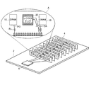
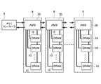
図1は、本発明を適用したメモリシステムの構造を模式的に示す略斜視図である。 FIG. 1 is a schematic perspective view schematically showing the structure of a memory system to which the present invention is applied.
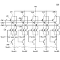
図1に示すメモリシステムは、いわゆるRDIMM(Registered Dual Inline Memory Module)を用いたメモリシステムであり、バスラインの駆動に用いる電源電圧VDDQのレベルを2段階に切り替え可能に構成されている。第1の電圧VDDQ1は相対的に高い電圧であり、例えば1.5Vである。また、第2の電圧VDDQ2は相対的に低い電圧であり、例えば1.25Vである。このように、本実施形態によるメモリシステムは、バスラインの駆動に用いる電源電圧VDDQをVDDQ1(1.5V)に設定して使用することも、VDDQ2(1.25V)に設定して使用することも可能である。電源電圧VDDQの切り替えに伴う動作については後述する。ここで、電源電圧VDDQとは、内部回路の動作電源となる電源電圧VDDとは異なる別系統の電源電圧である。但し、電源電圧VDDとVDDQのレベルは一致していても構わない。尚、正確には「電源電圧VDDQ」とは、高位側の電源電位VDDQと低位側の電源電位VSSQとの電位差を指す。 The memory system shown in FIG. 1 is a memory system using a so-called RDIMM (Registered Dual Inline Memory Module), and is configured to be able to switch the level of a power supply voltage VDDQ used for driving a bus line in two stages. The first voltage VDDQ1 is a relatively high voltage, for example, 1.5V. The second voltage VDDQ2 is a relatively low voltage, for example, 1.25V. As described above, the memory system according to the present embodiment can be used by setting the power supply voltage VDDQ used for driving the bus line to VDDQ1 (1.5V), or set to VDDQ2 (1.25V). Is also possible. The operation associated with the switching of the power supply voltage VDDQ will be described later. Here, the power supply voltage VDDQ is a power supply voltage of a different system different from the power supply voltage VDD serving as an operation power supply for the internal circuit. However, the levels of the power supply voltages VDD and VDDQ may be the same. To be precise, the “power supply voltage VDDQ” indicates a potential difference between the power supply potential VDDQ on the higher side and the power supply potential VSSQ on the lower side.
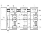
図1に示すように、本実施形態によるメモリシステムは、マザーボード2に複数のRDIMM4が装着された構成を有している。これらRDIMM4は、マザーボード2に実装されたメモリコントローラ6に接続されている。RDIMM4は、図1の拡大部Aに示すように、複数のDRAM10の他にレジスタチップ20が搭載されている。データDQ及びデータストローブ信号DQS,/DQS以外のコマンドアドレス信号CAについては、DRAM10に直接入力されるのではなく、レジスタチップ20によってバッファリングされた後、各DRAM10に供給される。
As shown in FIG. 1, the memory system according to the present embodiment has a configuration in which a plurality of
これに対し、データDQ及びデータストローブ信号DQS,/DQSについては、レジスタチップ20を経由することなく、メモリコントローラ6と各DRAM10との間で直接送受信される。図1に示す符号Rsは、スタブ抵抗である。以下の説明において、特に区別する必要がないときには、データDQ及びデータストローブ信号DQS,/DQSを単に「データDQ」と総称することがある。
On the other hand, the data DQ and the data strobe signals DQS and / DQS are directly transmitted and received between the
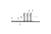
図2及び図3に示すように、各RDIMM4はメモリコントローラ6に対して共通接続される。図3においては、マザーボード2に設けられたデータ配線12がスタブ抵抗Rsを介して各RDIMM4の対応するDRAM10に共通接続された様子が示されている。このように、RDIMM方式では、DRAM10及びレジスタチップ20が複数のRDIMM間において共通接続される。
As shown in FIGS. 2 and 3, each
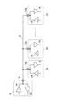
図4は、データDQの送受信に関わる要素を抜き出して示す回路図である。図4に示すように、メモリコントローラ6及びDRAM10に設けられたデータ入出力端子6a,10aは、データ配線12を介して共通接続されている。メモリコントローラ6及びDRAM10は、それぞれデータ入出力端子6a,10aに接続された出力回路14及び入力回路16を備えている。これにより、リード動作時においては、いずれかのDRAM10の出力回路14からデータDQが出力され、これがメモリコントローラ6内の入力回路16によって受信される。一方、ライト動作時においては、メモリコントローラ6内の出力回路14からデータDQが出力され、これがいずれかのDRAM10内の入力回路16によって受信される。本発明の特徴はこれら出力回路14にあり、その詳細については後述する。
FIG. 4 is a circuit diagram showing extracted elements related to transmission / reception of data DQ. As shown in FIG. 4, the data input /
尚、本発明をメモリシステムに適用した場合であっても、使用するメモリモジュールがRDIMMに限定されないことは言うまでもなく、FBDIMM(Fully Buffered DIMM)やUDIMM(Unbuffered DIMM)、LRDIMM(Load Reduced DIMM)等を用いることも可能である。 Even when the present invention is applied to a memory system, it goes without saying that the memory module to be used is not limited to RDIMM, FBDIMM (Fully Buffered DIMM), UDIMM (Unbuffered DIMM), LRDIMM (Load Reduced DIMM), etc. It is also possible to use.
図5に示すように、FBDIMM8はアドレス信号、データ信号、制御信号など全ての信号を一旦モジュール基板上に実装されたAMB(Advanced Memory Buffer)と呼ばれるチップ30で受けるタイプのDIMMである。AMB30はマザーボード2に実装されていても構わない。AMB30は、パラレル−シリアル変換機能を有するLSIチップである。つまり、AMB30とメモリコントローラ6との間は、PCIエクスプレスに似たポイント・ツー・ポイントのシリアルインタフェースで結ばれる。その一方で、AMB30とDRAM10間は、従来通りのパラレルインターフェースで結ばれる。AMB30は、シリアルに発行されたメモリ制御コマンドをパラレル変換し、まとめてDRAM10へ転送する。また、データDQを双方向転送する。
As shown in FIG. 5, the
図6は、FBDIMM方式における、データDQの送受信に関わる要素を抜き出して示す回路図である。図6に示すように、メモリコントローラ6と複数のAMB30との間は縦続接続されており、ライト時においてはデータ出力端子6b、データ入力端子30b、データ出力端子30cを介してライトデータが転送され、リード時においてはデータ出力端子30d、データ入力端子30e、データ入力端子6cを介してリードデータが転送される。一方、AMB30とDRAM10との間は、データ入出力端子10a,30aを介して個別に接続されている。データの転送には、出力回路14及び入力回路16が用いられる。上述の通り、本発明の特徴はこれら出力回路14にある。
FIG. 6 is a circuit diagram showing extracted elements related to transmission / reception of data DQ in the FBDIMM system. As shown in FIG. 6, the
図示しないが、UDIMMは、メモリコントローラ6からのアドレス信号、制御信号、データ信号が直接モジュール基板上のDRAM10に分配接続される形態のDIMMである。RDIMMやFBDIMMとは異なり、メモリコントローラ6とDRAM10との間に、レジスタチップ20やAMB30が介在しないことから、レイテンシ面では有利である。しかし、メモリコントローラ6及びDRAM10の双方から見た電気的な負荷が大きいことから、多くのDIMMを接続することには不向きである。図示しないが、LRDIMMにおいてはRDIMMのレジスタチップ20がメモリバッファに置き換えられる。また、RDIMMではメモリコントローラ6とDRAM10間でデータDQの授受が直接行われるが、LRDIMMではデータDQもメモリバッファを介してメモリコントローラ6とDRAM10間で授受が行われる。LRDIMMにおけるメモリバッファとDRAM10間のデータDQ信号の授受は、Point to Point topologyであり、FBDIMMと同様である。
Although not shown, the UDIMM is a DIMM in a form in which an address signal, a control signal, and a data signal from the
以下、図4及び図6に示した出力回路14の構成についてより詳細に説明する。
Hereinafter, the configuration of the
図7は、本発明の第1の実施形態による出力回路14の構成を示すブロック図である。
FIG. 7 is a block diagram showing a configuration of the
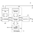
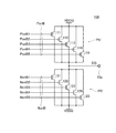
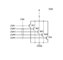
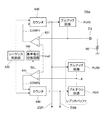
図7に示すように、本実施形態による出力回路14は、データ入出力端子10aを駆動する出力ドライバ100と、電源電圧VDDQに基づいて出力ドライバ100の特性を切り替える特性切替回路18とを備えている。特性切替回路18は、出力ドライバ100のスルーレートを調整するスルーレート制御回路200を含む。出力ドライバ100は、オン信号NonB,PonBに基づき、ハイレベル又はローレベルのデータDQをデータ入出力端子10aから出力する。特に限定されるものではないが、本実施形態においてはオン信号NonB,PonBはいずれも5ビットの信号である。これは、後述するように、出力ドライバ100に含まれるプルアップ回路PU及びプルダウン回路PDがいずれも5つの出力トランジスタによって構成されているためである。尚、出力回路14がODT(On Die Termination)機能を有している場合には、出力ドライバ100を終端抵抗として機能させることも可能である。出力ドライバ100の具体的な回路構成については後述する。
As shown in FIG. 7, the
スルーレート制御回路200は、オン信号PonA,NonA、スルーレート設定信号CP,CN及びソース電位VP,VNを受けて、オン信号PonB,NonBを生成する回路である。オン信号PonBは、論理的にはオン信号PonAの反転信号であるが、その波形及びレベルがスルーレート設定信号CP及びソース電位VPによって調整されている。同様に、オン信号NonBは、論理的にはオン信号NonAの反転信号であるが、その波形及びレベルがスルーレート設定信号CN及びソース電位VNによって調整されている。スルーレート制御回路200の具体的な回路構成については後述する。
The slew
スルーレート設定信号CP,CNは、スルーレート設定回路300から出力される信号であり、特に限定されるものではないが本実施形態ではそれぞれ3ビットの信号である。スルーレート設定信号CP,CNの値は、製造段階においてスルーレート設定回路300に対する不揮発的な書き込み(例えば、ヒューズ素子又はアンチヒューズ素子の破壊)を行うことによって固定される。製造段階におけるスルーレート設定回路300への書き込みは、ウェハ状態で行われる動作試験の結果や、当該半導体チップの用途などに基づいて行われる。したがって、スルーレート設定信号CP,CNにより設定されるスルーレートは、出荷時における最適な値である。但し、本発明においてスルーレート設定信号CP,CNを固定値とすることは必須でなく、可変としても構わない。
The slew rate setting signals CP and CN are signals output from the slew
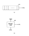
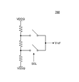
ソース電位VP,VNは、ソース電位調整回路400より供給される電位である。ソース電位調整回路400には切替信号SELが入力されており、生成されるソース電位VP,VNのレベルは切替信号SELによって選択される。切替信号SELは、電源電圧VDDQが相対的に高い電圧VDDQ1(1.5V)であるか、相対的に低い電圧VDDQ2(1.25V)であるかを示す信号である。切替信号SELは、図8(a)に示すように、電源電圧VDDQが第1のレベルVDDQ1であるか第2のレベルVDDQ2であるかを示すレジスタ410の設定値を参照することによって取得しても構わないし、図8(b)に示すように、電源電圧VDDQのレベルを検出する電圧検出回路420を用い、電圧検出回路420の検出結果を参照することによって取得しても構わない。本実施形態においては、電源電圧VDDQのレベルは、VDDQ1(1.5V)又はVDDQ2(1.25V)に設定されるため、切替信号SELは1ビットのデジタル信号で足りる。例えば、電源電圧VDDQのレベルがVDDQ1(1.5V)である場合には、切替信号SELはハイレベルとなり、電源電圧VDDQのレベルがVDDQ2(1.25V)である場合には、切替信号SELはローレベルとなる。但し、本発明がこれに限定されるものではない。例えば、図8(b)に示す電圧検出回路420を用いる場合には、電源電圧VDDQのレベル検出を無段階とし、切替信号SELをアナログ値としても構わない。
The source potentials VP and VN are potentials supplied from the source
オン信号PonA,NonAは、出力制御回路500から供給される信号であり、オン信号PonB,NonBと同様、本実施形態ではそれぞれ5ビットの信号である。出力制御回路500は、図示しない内部回路から供給される内部データP,N及びインピーダンス調整信号ZQP,ZQNを受けて、オン信号PonA,NonAを生成する。出力制御回路500の具体的な回路構成については後述する。
The on signals PonA and NonA are signals supplied from the
インピーダンス調整信号ZQP,ZQNは、キャリブレーション回路600より供給される信号である。詳細については後述するが、キャリブレーション回路600には、出力ドライバ100と実質的に同じ回路構成を有するレプリカバッファが含まれており、レプリカバッファを用いたキャリブレーション動作を行うことによって、インピーダンス調整信号ZQP,ZQNが生成される。このうち、インピーダンス調整信号ZQPは、出力ドライバ100に含まれるプルアップ回路を調整する信号であり、インピーダンス調整信号ZQNはプルダウン回路を調整する信号である。本実施形態においては、インピーダンス調整信号ZQP,ZQNはいずれも5ビットの信号である。
The impedance adjustment signals ZQP and ZQN are signals supplied from the
次に、図7に示す出力回路14を構成する各回路について詳細に説明する。
Next, each circuit constituting the
図9は、出力ドライバ100の回路図である。
FIG. 9 is a circuit diagram of the
図9に示すように、出力ドライバ100は、高位側の電源電位VDDQが供給される電源ラインとデータ入出力端子10aとの間に並列接続された複数(本実施形態では5つ)のPチャンネルMOSトランジスタからなる出力トランジスタ111〜115と、データ出力端子10aと低位側の電源電位VSSQが供給される電源ラインとの間に並列接続された複数(本実施形態では5つ)のNチャンネルMOSトランジスタからなる出力トランジスタ121〜125によって構成されている。出力ドライバ100のうち、出力トランジスタ111〜115からなる並列回路はプルアップ回路PUを構成しており、出力トランジスタ121〜125からなる並列回路はプルダウン回路PDを構成している。
As shown in FIG. 9, the
出力トランジスタ111〜115のゲート(制御電極)には、オン信号PonBを構成する5つの動作信号PonB1〜PonB5がそれぞれ供給されている。したがって、プルアップ回路PUを構成する出力トランジスタ111〜115は、動作信号PonB1〜PonB5に基づいて個々にオン(電気的に導通)/オフ(電気的に非導通)制御がされることになる。同様に、出力トランジスタ121〜125のゲート(制御電極)には、オン信号NonBを構成する5つの動作信号NonB1〜NonB5がそれぞれ供給されている。したがって、プルダウン回路PDを構成する出力トランジスタ121〜125も、動作信号NonB1〜NonB5に基づいて個々にオン/オフ制御がされることになる。尚、以後の説明において、トランジスタが電気的に導通する、または導通させることを、単に「オン」、トランジスタが電気的に非導通する、または非導通させることを、単に「オフ」と呼ぶことがある。
Five operation signals PonB1 to PonB5 constituting the ON signal PonB are supplied to the gates (control electrodes) of the output transistors 111 to 115, respectively. Accordingly, the output transistors 111 to 115 constituting the pull-up circuit PU are individually controlled to be on (electrically conductive) / off (electrically nonconductive) based on the operation signals PonB1 to PonB5. Similarly, five operation signals NonB1 to NonB5 constituting the ON signal NonB are supplied to the gates (control electrodes) of the
出力ドライバ100を構成するプルアップ回路PU及びプルダウン回路PDは、導通時に所定のインピーダンスとなるように設計されている。しかしながら、トランジスタのオン抵抗(トランジスタが電気的に導通する時のインピーダンス値)は製造条件によってばらつくとともに、動作時における環境温度や電源電圧によって変動することから、必ずしも所望のインピーダンスが得られるとは限らない。このため、実際のインピーダンスを所望の値とするためには、オンさせるべきトランジスタの数を調整する必要があり、かかる目的のために、複数の出力トランジスタからなる並列回路が用いられている。
The pull-up circuit PU and the pull-down circuit PD constituting the
出力ドライバ100のインピーダンスを微細且つ広範囲に調整するためには、プルアップ回路PU及びプルダウン回路PDを構成する複数の出力トランジスタのW/L比(ゲート幅/ゲート長比)を互いに異ならせることが好ましく、2のべき乗の重み付けをすることが特に好ましい。すなわち、出力トランジスタ111のW/L比を「1WLp」とした場合、出力トランジスタ112〜115のW/L比をそれぞれ「2WLp」、「4WLp」、「8WLp」、「16WLp」に設定することが特に好ましい。同様に、出力トランジスタ121のW/L比を「1WLn」とした場合、出力トランジスタ122〜125のW/L比をそれぞれ「2WLn」、「4WLn」、「8WLn」、「16WLn」に設定することが特に好ましい。
In order to finely adjust the impedance of the
このような構成により、動作信号PonB1〜PonB5,NonB1〜NonB5によってオンさせる出力トランジスタを適宜選択することで、製造条件によるばらつきや温度変化などにかかわらず、プルアップ回路PU及びプルダウン回路PDのインピーダンスを所望の値とすることが可能となる。 With such a configuration, by appropriately selecting output transistors that are turned on by the operation signals PonB1 to PonB5, NonB1 to NonB5, the impedances of the pull-up circuit PU and the pull-down circuit PD can be set regardless of variations due to manufacturing conditions or temperature changes. A desired value can be obtained.
但し、出力ドライバ100の構成としては図9に示す回路に限定されず、例えば図10に示すように、データ入出力端子10aとプルアップ回路PU及びプルダウン回路PDとの間に抵抗Rを挿入しても構わない。このような抵抗Rとしては、例えばタングステン(W)抵抗を用いることができる。
However, the configuration of the
図11は、スルーレート制御回路200のブロック図である。
FIG. 11 is a block diagram of the slew
図11に示すように、スルーレート制御回路200は、オン信号PonBを生成するスルーレート調整回路210と、オン信号NonBを生成するスルーレート調整回路220によって構成されている。スルーレート調整回路210は、スルーレート設定信号CP及びソース電位VPに基づき、オン信号PonAをオン信号PonBに変換する回路である。同様に、スルーレート調整回路220は、スルーレート設定信号CN及びソース電位VNに基づき、オン信号NonAをオン信号NonBに変換する回路である。
As shown in FIG. 11, the slew
上述の通り、オン信号PonBは、論理的にはオン信号PonAの反転信号であるが、その波形及びレベルがスルーレート設定信号CP及びソース電位VPによって調整されている。同様に、オン信号NonBは、論理的にはオン信号NonAの反転信号であるが、その波形及びレベルがスルーレート設定信号CN及びソース電位VNによって調整されている。 As described above, the ON signal PonB is logically an inverted signal of the ON signal PonA, but its waveform and level are adjusted by the slew rate setting signal CP and the source potential VP. Similarly, the ON signal NonB is logically an inverted signal of the ON signal NonA, but its waveform and level are adjusted by the slew rate setting signal CN and the source potential VN.
図12は、スルーレート調整回路210の回路図である。
FIG. 12 is a circuit diagram of the slew
図12に示すように、スルーレート調整回路210は、オン信号PonA1〜PonA5に基づいてそれぞれオン信号PonB1〜PonB5を生成する駆動回路231〜235によって構成されている。駆動回路231は、オン信号PonA1が供給されるNチャンネルMOSトランジスタ(選択トランジスタ)261〜263のそれぞれと、スルーレート設定信号CP1〜CP3が供給されるNチャンネルMOSトランジスタ(調整トランジスタ)271〜273のそれぞれとの直列回路が3つ並列接続された構成を有している。スルーレート設定信号CP1〜CP3は、スルーレート設定信号CPを構成する信号である。
As shown in FIG. 12, the slew
スルーレート設定信号CPを構成する各ビットCP1〜CP3に重み付けがされている場合には、少なくとも調整トランジスタ271〜273については重み付けに応じてW/L比(ゲート幅/ゲート長比)を互いに異ならせることが好ましい。具体的には、スルーレート設定CP1〜CP3の重み付けがそれぞれ「1」、「2」、「4」である場合には、調整トランジスタ271のW/L比を「1WLps」とした場合、調整トランジスタ272,273のW/L比をそれぞれ「2WLps」、「4WLps」に設定すればよい。
When the bits CP1 to CP3 constituting the slew rate setting signal CP are weighted, at least the
また、駆動回路231のソースには、ソース電位調整回路400より供給されるソース電位VPが供給される。ソース電位調整回路400は、切替信号SELがハイレベル(VDDQ=VDDQ1)である場合には、ソース電位VPをVSSに設定し、切替信号SELがローレベル(VDDQ=VDDQ2)である場合には、ソース電位VPをVSS未満の負電位VSS2に設定する。
The source potential VP supplied from the source
他の駆動回路232〜235についても、それぞれオン信号PonA2〜PonA5が供給される他は、駆動回路231と同じ回路構成を有している。
The
かかる回路構成により、対応するオン信号PonA1〜PonA5が活性レベル(ハイレベル)である駆動回路231〜235については、その出力であるオン信号PonB1〜PonB5がローレベル(VSS又はVSS2)に活性化する。オン信号PonB1〜PonB5は、オン信号PonA1〜PonA5が非活性レベル(ローレベル)に戻ると、Pチャンネル型MOSトランジスタ260によってハイレベルにリセットされる。
With this circuit configuration, for the
そして、オン信号PonA1〜PonA5の活性化に基づくオン信号PonB1〜PonB5の波形及びレベルは、スルーレート設定信号CP及びソース電位VPによって調整される。具体的には、スルーレート設定信号CPがより高いスルーレートを指定している場合には、オン信号PonB1〜PonB5の立ち下がりはより急峻となり、逆に、スルーレート設定信号CPがより低いスルーレートを指定している場合には、オン信号PonB1〜PonB5の立ち下がりはより緩やかとなる。また、電源電圧VDDQがVDD2(1.25V)に設定されている場合には、ソース電位VPがVSS2(<VSS)に設定されることから、ソース電位VPがVSSである場合に比べてスルーレートが高められる。 The waveforms and levels of the on signals PonB1 to PonB5 based on the activation of the on signals PonA1 to PonA5 are adjusted by the slew rate setting signal CP and the source potential VP. Specifically, when the slew rate setting signal CP designates a higher slew rate, the fall of the on signals PonB1 to PonB5 becomes steeper, and conversely, the slew rate setting signal CP has a lower slew rate. Is specified, the fall of the ON signals PonB1 to PonB5 becomes more gradual. When the power supply voltage VDDQ is set to VDD2 (1.25 V), the source potential VP is set to VSS2 (<VSS), so that the slew rate is compared with the case where the source potential VP is VSS. Is increased.
このようにして生成されるオン信号PonB1〜PonB5は、図9に示した出力ドライバ100のプルアップ回路PUに供給される。プルアップ回路PUは、Pチャンネル型MOSトランジスタ111〜115によって構成されていることから、そのオン抵抗(出力インピーダンス)は、ゲート−ソース間電圧(Vgs)及びソース−ドレイン間電圧(Vds)によって変化する。したがって、電源電圧VDDQが相対的に高いVDD1(1.5V)である場合のオン抵抗よりも、電源電圧VDDQが相対的に低いVDD2(1.25V)である場合のオン抵抗の方が高くなる。尚、本願明細書において、出力インピーダンスは、出力ドライバ100(プルアップ回路PUまたはプルダウン回路PD)が電気的に導通している場合の、インピーダンスを示す。更に、本願明細書において、インピーダンス値を単に「インピーダンス」と呼ぶ。
The ON signals PonB1 to PonB5 generated in this way are supplied to the pull-up circuit PU of the
しかしながら、本実施形態では、電源電圧VDDQがVDD2(1.25V)に設定されている場合には、ソース電位VPがVSSよりも低いVSS2に切り替えられるため、電源電圧VDDQがVDD1である場合のオン抵抗と、電源電圧VDDQがVDD2である場合のオン抵抗は等しくなる。より正確には、電源電圧VDDQがVDD1である場合のオン抵抗と、電源電圧VDDQがVDD2である場合のオン抵抗が等しくなるよう、VSS2のレベルが定められる。 However, in this embodiment, when the power supply voltage VDDQ is set to VDD2 (1.25 V), the source potential VP is switched to VSS2 lower than VSS, so that the on-state when the power supply voltage VDDQ is VDD1 is switched on. The resistance and the on-resistance when the power supply voltage VDDQ is VDD2 are equal. More precisely, the level of VSS2 is determined so that the on-resistance when the power supply voltage VDDQ is VDD1 and the on-resistance when the power supply voltage VDDQ is VDD2 are equal.
図13は、スルーレート調整回路220の回路図である。
FIG. 13 is a circuit diagram of the slew
図13に示すように、スルーレート調整回路220は、オン信号NonA1〜NonA5に基づいてそれぞれオン信号NonB1〜NonB5を生成する駆動回路241〜245によって構成されている。駆動回路241は、オン信号NonA1が供給されるNチャンネルMOSトランジスタ(選択トランジスタ)281〜283のそれぞれと、スルーレート設定信号CN1〜CN3が供給されるNチャンネルMOSトランジスタ(調整トランジスタ)291〜293のそれぞれとの直列回路が3つ並列接続された構成を有している。スルーレート設定信号CN1〜CN3は、スルーレート設定信号CNを構成する信号である。
As shown in FIG. 13, the slew
スルーレート設定信号CNを構成する各ビットCN1〜CN3に重み付けがされている場合には、少なくとも調整トランジスタ291〜293については重み付けに応じてW/L比(ゲート幅/ゲート長比)を互いに異ならせることが好ましい。具体的には、スルーレート設定CN1〜CN3の重み付けがそれぞれ「1」、「2」、「4」である場合には、調整トランジスタ291のW/L比を「1WLns」とした場合、調整トランジスタ292,293のW/L比をそれぞれ「2WLns」、「4WLns」に設定すればよい。
When the bits CN1 to CN3 constituting the slew rate setting signal CN are weighted, at least the
また、駆動回路241のソースには、ソース電位調整回路400より供給されるソース電位VNが供給される。ソース電位調整回路400は、切替信号SELがハイレベル(VDDQ=VDDQ1)である場合には、ソース電位VNをVDDに設定し、切替信号SELがローレベル(VDDQ=VDDQ2)である場合には、ソース電位VNをVDDを超える昇圧電位VDD2に設定する。
The source potential VN supplied from the source
他の駆動回路242〜245についても、それぞれオン信号NonA2〜NonA5が供給される他は、駆動回路241と同じ回路構成を有している。
The
かかる回路構成により、対応するオン信号NonA1〜NonA5が活性レベル(ローレベル)である駆動回路241〜245については、その出力であるオン信号NonB1〜NonB5がハイレベル(VDD又はVDD2)に活性化する。オン信号NonB1〜NonB5は、オン信号NonA1〜NonA5が非活性レベル(ハイレベル)に戻ると、Nチャンネル型MOSトランジスタ280によってローレベルにリセットされる。
With this circuit configuration, for the
そして、オン信号NonA1〜NonA5の活性化に基づくオン信号NonB1〜NonB5の波形及びレベルは、スルーレート設定信号CN及びソース電位VNによって調整される。具体的には、スルーレート設定信号CNがより高いスルーレートを指定している場合には、オン信号NonB1〜NonB5の立ち上がりはより急峻となり、逆に、スルーレート設定信号CNがより低いスルーレートを指定している場合には、オン信号NonB1〜NonB5の立ち上がりはより緩やかとなる。また、電源電圧VDDQがVDD2(1.25V)に設定されている場合には、ソース電位VNがVDD2(>VDD)に設定されることから、ソース電位VNがVDDである場合に比べてスルーレートが高められる。 The waveforms and levels of the on signals NonB1 to NonB5 based on the activation of the on signals NonA1 to NonA5 are adjusted by the slew rate setting signal CN and the source potential VN. Specifically, when the slew rate setting signal CN designates a higher slew rate, the rise of the on signals NonB1 to NonB5 becomes steeper, and conversely, the slew rate setting signal CN has a lower slew rate. When designated, the rise of the ON signals NonB1 to NonB5 becomes more gradual. Further, when the power supply voltage VDDQ is set to VDD2 (1.25 V), the source potential VN is set to VDD2 (> VDD), so that the slew rate is compared with the case where the source potential VN is VDD. Is increased.
このようにして生成されるオン信号NonB1〜NonB5は、図9に示した出力ドライバ100のプルダウン回路PDに供給される。プルダウン回路PDは、Nチャンネル型MOSトランジスタ121〜125によって構成されていることから、そのオン抵抗(出力インピーダンス)は、ゲート−ソース間電圧(Vgs)及びソース−ドレイン間電圧(Vds)によって変化する。したがって、電源電圧VDDQが相対的に高いVDD1(1.5V)である場合のオン抵抗よりも、電源電圧VDDQが相対的に低いVDD2(1.25V)である場合のオン抵抗の方が高くなる。
The ON signals NonB1 to NonB5 generated in this way are supplied to the pull-down circuit PD of the
しかしながら、本実施形態では、電源電圧VDDQがVDD2(1.25V)に設定されている場合には、ソース電位VNがVDDよりも高いVDD2に切り替えられるため、電源電圧VDDQがVDD1である場合のオン抵抗と、電源電圧VDDQがVDD2である場合のオン抵抗は等しくなる。より正確には、電源電圧VDDQがVDD1である場合のオン抵抗と、電源電圧VDDQがVDD2である場合のオン抵抗が等しくなるよう、VDD2のレベルが定められる。 However, in this embodiment, when the power supply voltage VDDQ is set to VDD2 (1.25 V), the source potential VN is switched to VDD2 higher than VDD, so that the on-state when the power supply voltage VDDQ is VDD1 is switched on. The resistance and the on-resistance when the power supply voltage VDDQ is VDD2 are equal. More precisely, the level of VDD2 is determined so that the on-resistance when the power supply voltage VDDQ is VDD1 and the on-resistance when the power supply voltage VDDQ is VDD2 are equal.
図14は、出力制御回路500の回路図である。
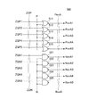
FIG. 14 is a circuit diagram of the
図14に示すように、出力制御回路500は、5つのNOR回路511〜515と、5つのNAND回路521〜525によって構成されている。NOR回路511〜515には内部データPが共通に供給されているとともに、インピーダンス調整信号ZQPを構成するインピーダンス調整信号ZQP1〜ZQP5がそれぞれ供給されている。一方、NAND回路521〜525には内部データNが共通に供給されているとともに、インピーダンス調整信号ZQNを構成するインピーダンス調整信号ZQN1〜ZQN5がそれぞれ供給されている。
As shown in FIG. 14, the
内部データP,Nは、出力すべきデータの論理値を示す信号であり、データ入出力端子10aより出力すべきデータがハイレベルであればいずれもローレベルとされ、データ入出力端子10aより出力すべきデータがローレベルであればいずれもハイレベルとされる。したがって、内部データP,Nを単一の信号とすることも可能であるが、出力ドライバ100がODT動作を行う場合には、内部データPをローレベル、内部データNをハイレベルとする必要があり、このようなケースを想定して本実施形態では別個の信号を用いている。上述の通り、内部データP,Nは図示しない内部回路によって生成される信号である。
The internal data P and N are signals indicating the logical value of the data to be output. If the data to be output from the data input /
このような構成により、内部データP,Nがローレベルである場合には、NOR回路511〜515の出力である動作信号PonA1〜PonA5の少なくとも一つがハイレベルに活性化する一方、NAND回路521〜525の出力である動作信号NonA1〜NonA5は全てハイレベルに非活性化される。この場合、動作信号PonA1〜PonA5のいずれを活性化させるかは、インピーダンス調整信号ZQPによって決まる。動作信号PonA1〜PonA5は、図7に示した動作信号PonAを構成する。
With such a configuration, when the internal data P and N are at the low level, at least one of the operation signals PonA1 to PonA5 that are the outputs of the NOR
同様に、内部データP,Nがハイレベルである場合には、NAND回路521〜525の出力である動作信号NonA1〜NonA5の少なくとも一つがローレベルに活性化する一方、NOR回路511〜515の出力である動作信号PonA1〜PonA5は全てローレベルに非活性化される。この場合、動作信号NonA1〜NonA5のいずれを活性化させるかは、インピーダンス調整信号ZQNによって決まる。動作信号NonA1〜NonA5は、図7に示した動作信号NonAを構成する。
Similarly, when the internal data P and N are at the high level, at least one of the operation signals NonA1 to NonA5 which are the outputs of the
図15は、キャリブレーション回路600の回路図である。
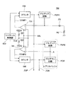
FIG. 15 is a circuit diagram of the
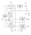
図15に示すように、キャリブレーション回路600は、プルアップ回路PUR1,PUR2と、プルダウン回路PDRと、プルアップ回路PUR1,PUR2の動作を制御するカウンタ630と、プルダウン回路PDRの動作を制御するカウンタ640と、カウンタ630,640をそれぞれ制御するコンパレータ631,641と、カウンタ630,640の動作を制御するシーケンス制御部650とを備えている。
As shown in FIG. 15, the
図16は、プルアップ回路PUR1の回路図である。 FIG. 16 is a circuit diagram of the pull-up circuit PUR1.
図16に示すように、プルアップ回路PUR1は、ドレインがキャリブレーション端子ZQに接続されている他は、出力ドライバ100に含まれるプルアップ回路PUと実質的に同じ回路構成を有している。具体的には、電源電位VDDQとキャリブレーション端子ZQとの間に並列接続された複数(本実施形態では5つ)のPチャンネルMOSトランジスタ611〜615によって構成されている。プルアップ回路PUR1に含まれるトランジスタ611〜615は、図9に示したトランジスタ111〜115に対応しており、それぞれ同一のインピーダンスを有している。但し、インピーダンスが実質的に同じである限り、プルアップ回路PUR1に含まれるトランジスタ611〜615と、図9に示したトランジスタ111〜115とが全く同じトランジスタサイズである必要はなく、シュリンクしたトランジスタを用いても構わない。
As shown in FIG. 16, the pull-up circuit PUR1 has substantially the same circuit configuration as the pull-up circuit PU included in the
図15に示したように、キャリブレーション端子ZQには外部抵抗REが接続されている。外部抵抗REのインピーダンスは、出力ドライバ100を構成するプルアップ回路PU及びプルダウン回路PDのインピーダンスと一致している。換言すれば、プルアップ回路PU及びプルダウン回路PDのインピーダンス目標値と同じインピーダンスをもった外部抵抗REがキャリブレーション端子ZQに接続される。
As shown in FIG. 15, an external resistor RE is connected to the calibration terminal ZQ. The impedance of the external resistor RE matches the impedance of the pull-up circuit PU and pull-down circuit PD that constitute the
トランジスタ611〜615のゲートには、カウンタ630よりインピーダンス調整信号ZQP1〜ZQP5がそれぞれ供給されており、これによってプルアップ回路PUR1の動作が制御される。インピーダンス調整信号ZQP1〜ZQP5は、図7に示したインピーダンス調整信号ZQPを構成する信号である。インピーダンス調整信号ZQP1〜ZQP5は、それぞれ出力ドライバ100を構成する出力トランジスタ111〜115に対応する信号であり、出力トランジスタ111〜115のうち使用する出力トランジスタを指定する。したがって、出力トランジスタ111〜115に重み付けがされている場合には、インピーダンス調整信号ZQP1〜ZQP5についても対応する重み付けを有する。
Impedance adjustment signals ZQP1 to ZQP5 are supplied from the
プルアップ回路PUR2は、ドレイン側が図15に示すノードAに接続されている他は、図16に示すプルアップ回路PUR1と同一の回路構成を有している。したがって、プルアップ回路PUR2に含まれる5つのトランジスタのゲートには、同じくインピーダンス調整信号ZQP1〜ZQP5が供給される。 The pull-up circuit PUR2 has the same circuit configuration as the pull-up circuit PUR1 shown in FIG. 16, except that the drain side is connected to the node A shown in FIG. Therefore, the impedance adjustment signals ZQP1 to ZQP5 are supplied to the gates of the five transistors included in the pull-up circuit PUR2.
図17は、プルダウン回路PDRの回路図である。 FIG. 17 is a circuit diagram of the pull-down circuit PDR.
図17に示すように、プルダウン回路PDRは、ドレインがノードAに接続されている他は、出力ドライバ100に含まれるプルダウン回路PDと実質的に同じ回路構成を有している。具体的には、ノードAと接地電位VSSQとの間に並列接続された複数(本実施形態では5つ)のNチャンネルMOSトランジスタ621〜625によって構成されている。プルダウン回路PDRに含まれるトランジスタ621〜625は、図9に示したトランジスタ121〜125に対応しており、それぞれ同一のインピーダンスを有している。但し、インピーダンスが実質的に同じである限り、プルダウン回路PDRに含まれるトランジスタ621〜625と、図9に示したトランジスタ121〜125とが全く同じトランジスタサイズである必要はなく、シュリンクしたトランジスタを用いても構わない。
As shown in FIG. 17, the pull-down circuit PDR has substantially the same circuit configuration as the pull-down circuit PD included in the
トランジスタ621〜625のゲートには、カウンタ640よりインピーダンス調整信号ZQN1〜ZQN5がそれぞれ供給されており、これによってプルダウン回路PDRの動作が制御される。インピーダンス調整信号ZQN1〜ZQN5は、図7に示したインピーダンス調整信号ZQNを構成する信号である。インピーダンス調整信号ZQN1〜ZQN5は、それぞれ出力ドライバ100を構成する出力トランジスタ121〜125に対応する信号であり、出力トランジスタ121〜125のうち使用する出力トランジスタを指定する。したがって、出力トランジスタ121〜125に重み付けがされている場合には、インピーダンス調整信号ZQN1〜ZQN5についても対応する重み付けを有する。
Impedance adjustment signals ZQN1 to ZQN5 are supplied from the
図15に示すように、プルアップ回路PUR2とプルダウン回路PDRはノードAを介して接続されている。このため、プルアップ回路PUR2とプルダウン回路PDRは、出力ドライバ100と実質的に同じ回路構成を有するレプリカバッファを構成する。ここでいう「実質的に同じ」とは、レプリカバッファに含まれるトランジスタがシュリンクされている場合であっても同じとみなす意である。レプリカバッファの出力端であるノードAは、図15に示すように、コンパレータ641の非反転入力端子(+)に接続されている。
As shown in FIG. 15, the pull-up circuit PUR2 and the pull-down circuit PDR are connected via the node A. For this reason, the pull-up circuit PUR2 and the pull-down circuit PDR constitute a replica buffer having substantially the same circuit configuration as that of the
カウンタ630は、コンパレータ631の出力に応じてカウントアップ又カウントダウンするカウンタであり、その出力はインピーダンス調整信号ZQPとして用いられる。カウンタ630は、コンパレータ631の出力である比較信号COMP1がハイレベルである場合にはカウントアップを行い、比較信号COMP1がローレベルである場合にはカウントダウンを行う。コンパレータ631の非反転入力端子(+)はキャリブレーション端子ZQに接続されており、反転入力端子(−)は電源電位VDDQと接地電位VSSQとの間に接続された抵抗661,662の中点に接続されている。尚、接地電位VSSQは、低電位側である低電位電源ラインである。かかる構成により、コンパレータ631は、キャリブレーション端子ZQの電位と中間電圧(VDDQ/2)とを比較し、前者の電位が後者の電位よりも高ければその出力である比較信号COMP1をハイレベルとし、後者の電位が前者の電位よりも高ければ比較信号COMP1をローレベルとする。
The
尚、コンパレータ631と641のそれぞれの反転入力端子(−)に入力される抵抗661,662の中点(Vref)の電位は、VDDQの電位が変われば、それに対応して変更されることに注意が必要である。即ち、中点の電位である所定電圧は、電源電圧(VDDQ)が第1の電圧(1.5V)である場合、第1の電圧に対して1/n(抵抗661,662の比)である第1の所定電圧であり、電源電圧(VDDQ)が第2の電圧(1.25V)である場合、第2の電圧に対して前記1/nである第2の所定電圧である。1/nは、例えば1/2である。即ち、nは2であり、この値「2」はJEDECで規格化されたZQ端子を使用したキャリブレーション(出力トランジスタのインピーダンスをマッチングさせるに当たり、出力トランジスタのインピーダンス値とキャリブレーション抵抗(RE)値とをマッチングさせる。)がマッチングしたときのZQ端子の電位(VDDQ/2)の「2」に相当する値である。
Note that the potential of the middle point (Vref) of the
一方、カウンタ640は、コンパレータ641の出力に応じてカウントアップ又カウントダウンするカウンタであり、その出力はインピーダンス調整信号ZQNとして用いられる。カウンタ640は、コンパレータ641の出力である比較信号COMP2がハイレベルである場合にはカウントアップを行い、比較信号COMP2がローレベルである場合にはカウントダウンを行う。コンパレータ641の非反転入力端子(+)はノードAに接続されており、反転入力端子(−)は抵抗661,662の中点に接続されている。かかる構成により、コンパレータ641は、ノードAの電位と中間電圧(VDDQ/2)とを比較し、前者の方が電位が高ければその出力である比較信号COMP2をハイレベルとし、後者の方が電位が高ければ比較信号COMP2をローレベルとする。
On the other hand, the
そして、カウンタ630,640はシーケンス制御部650による制御によりカウント動作を行い、これにより、プルアップ回路PUR1,PUR2及びプルダウン回路PDRのインピーダンスを調整する。
The
図18は、キャリブレーション回路600の動作を示すフローチャートである。
FIG. 18 is a flowchart showing the operation of the
まず、外部からキャリブレーションコマンドが発行されると(ステップS1)、シーケンス制御部650はカウンタ630の動作を許可する。これにより、プルアップ回路PUR1のインピーダンスが外部抵抗REのインピーダンスと一致するよう、カウンタ630のカウント値が定められる(ステップS2)。具体的には、キャリブレーション端子ZQの電位が中間電圧(VDDQ/2)よりも高ければ、比較信号COMP1がハイレベルとなることから、カウンタ630はカウントアップを行う。これにより、プルアップ回路PUR1のインピーダンスは徐々に高められる。逆に、キャリブレーション端子ZQの電位が中間電圧(VDDQ/2)よりも低ければ、比較信号COMP1がローレベルとなることから、カウンタ630はカウントダウンを行う。これにより、プルアップ回路PUR1のインピーダンスは徐々に下げられる。
First, when a calibration command is issued from the outside (step S1), the
このような動作を行うことにより、カウンタ630のカウント値であるインピーダンス調整信号ZQPは、プルアップ回路PUR1のインピーダンスが外部抵抗REのインピーダンスと一致するような値に調整される。図15に示すように、インピーダンス調整信号ZQPはプルアップ回路PUR2にも供給されていることから、プルアップ回路PUR2についてもインピーダンスが外部抵抗REのインピーダンスと一致する。
By performing such an operation, the impedance adjustment signal ZQP which is the count value of the
プルアップ回路PUR1,PUR2の調整が終わると、シーケンス制御部650はカウンタ640の動作を許可し、プルダウン回路PDRの調整を行う(ステップS3)。具体的には、ノードAの電位が中間電圧(VDDQ/2)よりも高ければ、比較信号COMP2がハイレベルとなることから、カウンタ640はカウントアップを行う。これにより、プルダウン回路PDRのインピーダンスは徐々に下げられる。逆に、ノードAの電位が中間電圧(VDDQ/2)よりも低ければ、比較信号COMP2がローレベルとなることから、カウンタ640はカウントダウンを行う。これにより、プルダウン回路PDRのインピーダンスは徐々に高められる。
When the adjustment of the pull-up circuits PUR1 and PUR2 is completed, the
このような動作を行うことにより、カウンタ640のカウント値であるインピーダンス調整信号ZQNは、プルダウン回路PDRのインピーダンスがプルアップ回路PUR2のインピーダンスと一致するような値に調整される。上述の通り、プルアップ回路PUR2のインピーダンスは外部抵抗REのインピーダンスと一致していることから、上記の動作によって、プルダウン回路PDRについてもインピーダンスが外部抵抗REのインピーダンスと一致することになる。
By performing such an operation, the impedance adjustment signal ZQN that is the count value of the
このようにして生成されたインピーダンス調整信号ZQP,ZQNは、図7に示すように出力制御回路500に供給される。
The impedance adjustment signals ZQP and ZQN generated in this way are supplied to the
以上が図7に示す出力回路14の構成とその動作である。次に、電源電圧VDDQのレベルと出力されるデータDQとの関係について説明する。
The above is the configuration and operation of the
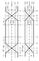
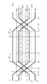
図19は、出力ドライバ100から出力されるデータDQの波形図であり、(a)は電源電圧VDDQが第1の電圧VDDQ1(1.5V)である場合を示し、(b)は電源電圧VDDQが第2の電圧VDDQ2(1.25V)である場合を示している。図19(a),(b)に示す符号41,51は、データDQがハイレベル、ローレベル、ハイレベルの順に変化する場合の波形であり、符号42,52は、データDQがローレベル、ハイレベル、ローレベルの順に変化する場合の波形である。
FIG. 19 is a waveform diagram of data DQ output from the
図19(a),(b)に示すように、データDQがハイレベルからローレベルに変化する場合、時刻t10(t16)においてハイレベルである+AC1又は+AC2から低下を始め、時刻t12(t18)にて中間レベル(VDDQ/2)に達し、時刻t13(t19)にてローレベルである−AC1又は−AC2に到達する。これら+AC1,+AC2,−AC1,−AC2はいずれもACレベルであり、それぞれ中間レベル(VDDQ/2)を基準として+150mV,+125mV,−150mV,−125mVである。したがって、図19(a)に示すように、電源電圧VDDQが第1の電圧VDDQ1(1.5V)である場合には、中間レベル(VDDQ/2)が750mVであることから、+AC1のレベルは900mV、−AC1のレベルは600mVとなる。一方、図19(b)に示すように、電源電圧VDDQが第2の電圧VDDQ2(1.25V)である場合には、中間レベル(VDDQ/2)が625mVであることから、+AC2のレベルは750mV、−AC2のレベルは500mVとなる。 As shown in FIGS. 19A and 19B, when the data DQ changes from the high level to the low level, it starts to decrease from + AC1 or + AC2 which is the high level at time t10 (t16), and time t12 (t18). Reaches the intermediate level (VDDQ / 2) at time t13 (t19) and reaches the low level -AC1 or -AC2. These + AC1, + AC2, -AC1, and -AC2 are all at the AC level, and are +150 mV, +125 mV, -150 mV, and -125 mV with respect to the intermediate level (VDDQ / 2), respectively. Accordingly, as shown in FIG. 19A, when the power supply voltage VDDQ is the first voltage VDDQ1 (1.5 V), the intermediate level (VDDQ / 2) is 750 mV, so the level of + AC1 is The level of 900 mV and -AC1 is 600 mV. On the other hand, as shown in FIG. 19B, when the power supply voltage VDDQ is the second voltage VDDQ2 (1.25 V), the intermediate level (VDDQ / 2) is 625 mV, so the level of + AC2 is The level of 750 mV and -AC2 is 500 mV.
したがって、電源電圧VDDQが第1の電圧VDDQ1(1.5V)である場合の振幅(ここではPeak to Peak電圧、以下同様)は300mV、電源電圧VDDQが第2の電圧VDDQ2(1.5V)である場合の振幅は250mVとなり、電源電圧VDDQの値に応じて振幅がスケーリング(×0.83倍)されていることが分かる。 Therefore, when the power supply voltage VDDQ is the first voltage VDDQ1 (1.5 V), the amplitude (Peak to Peak voltage, hereinafter the same) is 300 mV, and the power supply voltage VDDQ is the second voltage VDDQ2 (1.5 V). In some cases, the amplitude is 250 mV, and it can be seen that the amplitude is scaled (× 0.83) in accordance with the value of the power supply voltage VDDQ.
尚、図19(a),(b)に示す+DC1,+DC2,−DC1,−DC2はいずれもDCレベルであり、それぞれ中間レベル(VDDQ/2)を基準として+100mV,+83.3mV,−100mV,−83.3mVである。また、図19(a)に示す符号SRF1は、電源電圧VDDQが第1の電圧VDDQ1(1.5V)である場合の立ち下がり時におけるスルーレートであり、符号SRR1は、電源電圧VDDQが第1の電圧VDDQ1(1.5V)である場合の立ち上がり時におけるスルーレートである。本実施形態では、SRF1=SRR1=1V/nsである。同様に、図19(b)に示す符号SRF2は、電源電圧VDDQが第2の電圧VDDQ2(1.25V)である場合の立ち下がり時におけるスルーレートであり、符号SRR2は、電源電圧VDDQが第2の電圧VDDQ2(1.25V)である場合の立ち上がり時におけるスルーレートである。本実施形態では、SRF2=SRR2=0.83V/nsである。 Note that + DC1, + DC2, -DC1, and -DC2 shown in FIGS. 19A and 19B are all DC levels, and +100 mV, +83.3 mV, and -100 mV, respectively, with reference to the intermediate level (VDDQ / 2). -83.3 mV. Further, symbol SRF1 shown in FIG. 19A is a slew rate at the fall time when the power supply voltage VDDQ is the first voltage VDDQ1 (1.5 V), and symbol SRR1 is the first power supply voltage VDDQ is the first voltage VDDQ1. The slew rate at the rise when the voltage VDDQ1 is 1.5V. In the present embodiment, SRF1 = SRR1 = 1 V / ns. Similarly, symbol SRF2 shown in FIG. 19B is a slew rate at the time of falling when the power supply voltage VDDQ is the second voltage VDDQ2 (1.25 V), and symbol SRR2 is the power supply voltage VDDQ at the first voltage. This is the slew rate at the rise when the voltage VDDQ2 (1.25 V) is 2. In the present embodiment, SRF2 = SRR2 = 0.83 V / ns.
図20は、図19(a)と図19(b)を重ね合わせた図である。 FIG. 20 is a diagram in which FIG. 19A and FIG.
図20から明らかなように、本実施形態では、電源電圧VDDQが第1の電圧VDDQ1(1.5V)である場合と第2の電圧VDDQ2(1.25V)である場合とで、データDQの変化における絶対時間が一致していることが分かる。つまり、立ち上がり又は立ち下がりの開始タイミング、立ち上がり又は立ち下がりの完了タイミング、さらには、基準電位である中間レベル(VDDQ/2)とのクロスポイントが互いに同じである。さらに詳細には、立ち上がり又は立ち下がりの完了(ACレベルが±AC1又は±AC2に到達したタイミングである時刻t13(t19))を基準としたセットアップ時間tS(t13〜t14;例えば75ps)も同じにできる。立ち上がり又は立ち下がりの開始(DCレベルが±DC1又は±DC2に到達したタイミングである時刻t11(t17))を基準としたホールド時間tH(t15〜t17;例えば100ps)も同じにできる。実際のデータ転送においては、データストローブ信号DQS,/DQSのクロスポイントが図20に示す時刻t14から時刻t15の間にあれば、レシーバ側にて正しく受信を行うことができる。そして、本実施形態では、時刻t14を決めるセットアップ時間tSや、時刻t15を決めるホールド時間tHが電源電圧VDDQによらず同一にできることから、電源電圧VDDQのレベルを切替えた場合であっても、正しくデータを受信することが可能となる。この際、レシーバの特性としては、第1の電圧VDDQ1である場合のレシーバの特性が図31,図32の場合、第2の電圧VDDQ2である場合のレシーバの特性を図33,図34のような特性にすれば良い。しかし通常は調整不要であり、そのままで正しく受信可能である。つまり、第2の電圧VDDQ2(1.25V)のシステムは、第1の電圧VDDQ1(1.5V)のシステムの資産(マザーボードやDIMM基板等のハード、MRS(モードレジスタ)設定値等のソフトウェア、並びにそのシステムに搭載されるデバイス)をそのまま利用することが可能である。 As is apparent from FIG. 20, in the present embodiment, the data DQ of the data DQ is different depending on whether the power supply voltage VDDQ is the first voltage VDDQ1 (1.5 V) or the second voltage VDDQ2 (1.25 V). It can be seen that the absolute times of change are consistent. That is, the start timing of the rise or fall, the completion timing of the rise or fall, and the cross point with the intermediate level (VDDQ / 2) as the reference potential are the same. More specifically, the setup time tS (t13 to t14; for example, 75 ps) based on the completion of rising or falling (time t13 (t19), which is the timing when the AC level reaches ± AC1 or ± AC2) is the same. it can. The hold time tH (t15 to t17; for example, 100 ps) based on the start of rising or falling (time t11 (t17), which is the timing when the DC level reaches ± DC1 or ± DC2) can be made the same. In actual data transfer, if the cross point of the data strobe signals DQS and / DQS is between time t14 and time t15 shown in FIG. 20, reception can be performed correctly on the receiver side. In this embodiment, the setup time tS for determining the time t14 and the hold time tH for determining the time t15 can be made the same regardless of the power supply voltage VDDQ. Therefore, even when the level of the power supply voltage VDDQ is switched, Data can be received. At this time, as receiver characteristics, when the first voltage VDDQ1 is the receiver characteristic shown in FIGS. 31 and 32, the receiver characteristics when the second voltage VDDQ2 is shown in FIGS. 33 and 34 are shown. It is sufficient to make it a characteristic. However, adjustment is usually unnecessary and reception is possible as it is. That is, the system of the second voltage VDDQ2 (1.25V) is a system asset of the first voltage VDDQ1 (1.5V) (hardware such as a mother board or a DIMM board, software such as an MRS (mode register) setting value, In addition, a device mounted on the system can be used as it is.
このような動作を実現するためには、出力ドライバ100のオン抵抗(出力インピーダンス)を、電源電圧VDDQが第1の電圧VDDQ1(1.5V)である場合と電源電圧VDDQが第2の電圧VDDQ2(1.25V)である場合とで一致させればよい。しかしながら、出力ドライバ100を構成する出力トランジスタのゲート電圧を電源電圧VDDQに単純に連動させてしまうと、電源電圧VDDQが第1の電圧VDDQ1(1.5V)である場合のオン抵抗よりも、電源電圧VDDQが第2の電圧VDDQ2(1.25V)である場合のオン抵抗の方が、自然法則により高くなってしまう。本実施形態では、電源電圧VDDQによらずオン抵抗を一致させるため、上述の通り、ソース電位調整回路400を用いて、導通時における出力トランジスタのゲート電圧を切り替えている。
In order to realize such an operation, the ON resistance (output impedance) of the
但し、電源電圧VDDQが第1の電圧VDDQ1(1.5V)である場合と第2の電圧VDDQ2(1.25V)である場合とで出力ドライバ100のオン抵抗を一致させる方法としては、上記の方法に限定されるものではなく、他の方法を用いても構わない。例えば、キャリブレーション回路600を用いたキャリブレーション動作によってオン抵抗を調整し、これにより、電源電圧VDDQによらずオン抵抗を一致させることも可能である。但し、電源電圧VDDQが低くなると出力トランジスタのオン抵抗が高くなることから、キャリブレーション回路600のみによってオン抵抗の調整を行うためには、プルアップ回路PUやプルダウン回路PDを構成する並列な出力トランジスタの数を増やす必要がある。もちろん、低電圧で使用する場合のトランジスタ性能を向上させて、オン抵抗を一致させることも可能である。
However, as a method of matching the on-resistance of the
次に、本実施形態による効果について図面を用いて説明する。 Next, the effect by this embodiment is demonstrated using drawing.
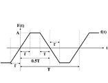
図21は、周期的台形波の波形モデルであり、周期T、振幅A、立ち上がり及び立ち下がり遷移時間2τである場合を示している。このような周期的台形波f(t)は、次式で表すことができる。 FIG. 21 is a waveform model of a periodic trapezoidal wave, and shows a case where the period is T, the amplitude is A, and the rising and falling transition times are 2τ. Such a periodic trapezoidal wave f (t) can be expressed by the following equation.

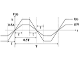
図22は、振幅Aの周期的台形波f(t)と振幅0.5Aの周期的台形波g(t)を重ね合わせた波形図である。周期的台形波g(t)は、次式で表すことができる。 FIG. 22 is a waveform diagram in which a periodic trapezoidal wave f (t) having an amplitude A and a periodic trapezoidal wave g (t) having an amplitude of 0.5A are superimposed. The periodic trapezoidal wave g (t) can be expressed by the following equation.
式(1)及び式(2)から分かるように、周期的台形波f(t)と周期的台形波g(t)は、周波数成分係数が同じである。このことは、振幅が変化しても遷移時間が同じであれば信号の高調波成分が変化せず、その結果、電源電圧を低下させても同じ品質の波形がレシーバに到達することを意味する。すなわち、本実施形態によれば、電源電圧VDDQを第1の電圧VDDQ1(1.5V)から第2の電圧VDDQ2(1.25V)に切り替えても、レシーバ側は(新たな仕組みを組み込むことなく)そのまま受信可能となる。 As can be seen from the equations (1) and (2), the periodic trapezoidal wave f (t) and the periodic trapezoidal wave g (t) have the same frequency component coefficient. This means that even if the amplitude changes, if the transition time is the same, the harmonic component of the signal does not change, and as a result, the waveform of the same quality reaches the receiver even if the power supply voltage is lowered. . That is, according to the present embodiment, even if the power supply voltage VDDQ is switched from the first voltage VDDQ1 (1.5 V) to the second voltage VDDQ2 (1.25 V), the receiver side (without incorporating a new mechanism) ) It can be received as it is.
図23(a)は伝送系のモデル図であり、図23(b)は各点の信号波形を示す模式図である。図23(a)に示す抵抗Ronは、出力ドライバ100のオン抵抗を示している。また、伝送線路Z0は、チップ間を接続する配線であり、例えば図3及び図4に示したデータ配線12に相当する。さらに、抵抗Rttは、伝送線路Z0(データ配線12)に接続された終端抵抗であり、中間電位VTT(=VDDQ/2)に接続されている。実際にはテブナン終端が用いられる場合もある。
FIG. 23A is a model diagram of a transmission system, and FIG. 23B is a schematic diagram showing signal waveforms at respective points. A resistor Ron shown in FIG. 23A indicates the on-resistance of the
図23(b)に示すように、信号源Vの出力Vinが0VからVDDQまで、立ち上がり時間tRで変化した場合、A点の電位も時間tRで立ち上がる。これが伝送線路Z0を伝搬し、B点に伝達される。図23(b)に示す例では、伝送線路Z0の伝搬時間Tdは1000psである。 As shown in FIG. 23B, when the output Vin of the signal source V changes from 0 V to VDDQ at the rising time tR, the potential at the point A also rises at the time tR. This propagates through the transmission line Z0 and is transmitted to point B. In the example shown in FIG. 23B, the propagation time Td of the transmission line Z0 is 1000 ps.
このようなモデルにおいて、図24に示すように、電源電圧VDDQが1.5Vである場合と1.25Vである場合を考えると、抵抗Ronが等しければ、A点の振幅がスケーリングされるだけであり、A点の電位変化に要する時間は変化しない。本実施形態は、ソース電位調整回路400を用いて出力ドライバ100のオン抵抗を調整することにより、このような条件を満たすよう調整しているのである。
In such a model, as shown in FIG. 24, considering the case where the power supply voltage VDDQ is 1.5 V and the case where it is 1.25 V, if the resistance Ron is equal, only the amplitude of the point A is scaled. Yes, the time required to change the potential at point A does not change. In the present embodiment, the source
また、電源電圧VDDQに応じて信号の振幅をスケーリングし、且つ、信号の立ち上がり時間及び立ち下がり時間が一定であれば、クロストーク成分もスケーリングされる。したがって、電源電圧VDDQを変化させても、信号に対するクロストークの影響は変わらない。同様に反射の影響も変わらない。 Further, if the amplitude of the signal is scaled according to the power supply voltage VDDQ and the rise time and fall time of the signal are constant, the crosstalk component is also scaled. Therefore, even if the power supply voltage VDDQ is changed, the influence of crosstalk on the signal does not change. Similarly, the influence of reflection does not change.
次に、本発明の好ましい第2の実施形態について説明する。 Next, a second preferred embodiment of the present invention will be described.
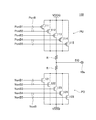
図25は、本発明の第2の実施形態による出力回路14aの構成を示すブロック図である。
FIG. 25 is a block diagram showing a configuration of the
図25に示すように、本実施形態による出力回路14aは、切替信号SELが特性切替回路18aに含まれるキャリブレーション回路700にも入力されている点において、図7に示した出力回路14と相違している。その他の構成については、図7に示した出力回路14と同一であることから、同一の要素には同一の符号を付し、重複する説明は省略する。
As shown in FIG. 25, the
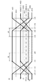
図26は、本実施形態において出力ドライバ100から出力されるデータDQの波形図であり、電源電圧VDDQが第1の電圧VDDQ1(1.5V)である場合の波形と、電源電圧VDDQが第2の電圧VDDQ2(1.25V)である場合の波形を重ねて示している。
FIG. 26 is a waveform diagram of data DQ output from the
図26に示すように、電源電圧VDDQが第1の電圧VDDQ1(1.5V)である場合の波形は、図19(a)に示した波形と同じである。これに対し、電源電圧VDDQが第2の電圧VDDQ2(1.25V)である場合の波形は、図19(b)に示した波形とは異なり、振幅が拡大されている。具体的には、電源電圧VDDQが第1の電圧VDDQ1(1.5V)である場合の振幅と、電源電圧VDDQが第2の電圧VDDQ2(1.25V)である場合の振幅が一致している。つまり、中間レベル(VDDQ/2)を基準とした+AC2a及び−AC2aの値は、それぞれ中間レベル(VDDQ/2)を基準とした+AC1及び−AC1値(±150mV)と一致している。同様に、中間レベル(VDDQ/2)を基準とした+DC2a及び−DC2aの値も、それぞれ中間レベル(VDDQ/2)を基準とした+DC1及び−DC1値(±100mV)と一致している。 As shown in FIG. 26, the waveform when the power supply voltage VDDQ is the first voltage VDDQ1 (1.5 V) is the same as the waveform shown in FIG. On the other hand, the waveform when the power supply voltage VDDQ is the second voltage VDDQ2 (1.25 V) is different from the waveform shown in FIG. Specifically, the amplitude when the power supply voltage VDDQ is the first voltage VDDQ1 (1.5V) and the amplitude when the power supply voltage VDDQ is the second voltage VDDQ2 (1.25V) match. . That is, the values of + AC2a and −AC2a with the intermediate level (VDDQ / 2) as a reference are the same as the + AC1 and −AC1 values (± 150 mV) with the intermediate level (VDDQ / 2) as a reference. Similarly, the values of + DC2a and −DC2a with the intermediate level (VDDQ / 2) as a reference also coincide with the + DC1 and −DC1 values (± 100 mV) with the intermediate level (VDDQ / 2) as a reference.
その他の点については、第1の実施形態と同様である。したがって、電源電圧VDDQが第1の電圧VDDQ1(1.5V)である場合と第2の電圧VDDQ2(1.25V)である場合とで、データDQの変化における絶対時間については完全に一致している。つまり、立ち上がり又は立ち下がりの開始タイミング、立ち上がり又は立ち下がりの完了タイミング、さらには、基準電位である中間レベル(VDDQ/2)とのクロスポイントが互いに同じである。セットアップ時間tSやホールド時間tHも同じにできる。したがって、実際のデータ転送においては、データストローブ信号のクロスポイントが図26に示す時刻t14から時刻t15の間にあれば、レシーバ側にて正しく受信を行うことができる。そして、本実施形態では、時刻t14を決めるセットアップ時間tSや、時刻t15を決めるホールド時間tHが電源電圧VDDQによらず一定にできることから、電源電圧VDDQを切り替えた場合であっても、正しく(第1の電圧VDDQ1(1.5V)時の受信品質で)データを受信することが可能となる。この際、レシーバの特性としては、第1の電圧VDDQ1である場合のレシーバの特性が図35,図36の場合、第2の電圧VDDQ2である場合のレシーバの特性を図37,図38のような特性にすれば良い。しかし通常は調整不要であり、そのままで正しく受信可能である。つまり、第2の電圧VDDQ2(1.25V)のシステムは、第1の電圧VDDQ1(1.5V)のシステムの資産(マザーボードやDIMM基板等のハード、MRS(モードレジスタ)設定値等のソフトウェア、並びにそのシステムに搭載されるデバイス)をそのまま利用することが可能である。 The other points are the same as in the first embodiment. Therefore, the absolute time in the change of the data DQ is completely the same when the power supply voltage VDDQ is the first voltage VDDQ1 (1.5V) and when the power supply voltage VDDQ is the second voltage VDDQ2 (1.25V). Yes. That is, the start timing of the rise or fall, the completion timing of the rise or fall, and the cross point with the intermediate level (VDDQ / 2) as the reference potential are the same. The setup time tS and hold time tH can be made the same. Therefore, in actual data transfer, if the cross point of the data strobe signal is between time t14 and time t15 shown in FIG. 26, reception can be performed correctly on the receiver side. In the present embodiment, the setup time tS for determining the time t14 and the hold time tH for determining the time t15 can be made constant irrespective of the power supply voltage VDDQ. Therefore, even when the power supply voltage VDDQ is switched, It is possible to receive data (with reception quality at a voltage VDDQ1 (1.5V) of 1). At this time, as the receiver characteristics, the receiver characteristics when the first voltage VDDQ1 is the case shown in FIGS. 35 and 36, and the receiver characteristics when the second voltage VDDQ2 is used are as shown in FIGS. It is sufficient to make it a characteristic. However, adjustment is usually unnecessary and reception is possible as it is. That is, the system of the second voltage VDDQ2 (1.25V) is a system asset of the first voltage VDDQ1 (1.5V) (hardware such as a mother board or a DIMM board, software such as an MRS (mode register) setting value, In addition, a device mounted on the system can be used as it is.
本実施形態では、電源電圧VDDQが第1の電圧VDDQ1(1.5V)である場合のスルーレートと、電源電圧VDDQが第2の電圧VDDQ2(1.25V)である場合のスルーレートは一致する。かかる制御は、ソース電位調整回路400によるソース電位の調整によって実現される。
In this embodiment, the slew rate when the power supply voltage VDDQ is the first voltage VDDQ1 (1.5 V) and the slew rate when the power supply voltage VDDQ is the second voltage VDDQ2 (1.25 V) match. . Such control is realized by adjusting the source potential by the source
また、本実施形態では、電源電圧VDDQが第1の電圧VDDQ1(1.5V)である場合の振幅と、電源電圧VDDQが第2の電圧VDDQ2(1.25V)である場合の振幅を一致させるため、出力ドライバ100のオン抵抗(出力インピーダンス)を、電源電圧VDDQが第1の電圧VDDQ1(1.5V)である場合よりも、電源電圧VDDQが第2の電圧VDDQ2(1.25V)である場合の方が低くなるよう設定している。より具体的には、電源電圧VDDQが第1の電圧VDDQ1である場合の出力インピーダンスをRon1、電源電圧VDDQが第2の電圧VDDQ2である場合の出力インピーダンスをRon2、出力ドライバ100に接続される終端抵抗の抵抗値をRttとした場合、
Ron2=Ron1(VDDQ2/VDDQ1)−Rtt{1−(VDDQ2/VDDQ1)}
を満たせば、電源電圧VDDQが第1の電圧VDDQ1(1.5V)である場合の振幅と、電源電圧VDDQが第2の電圧VDDQ2(1.25V)である場合の振幅が一致する。本実施形態では、この条件を満足すべく、切替信号SELによってソース電位調整回路400及びキャリブレーション回路700の動作を切り替えている。
In the present embodiment, the amplitude when the power supply voltage VDDQ is the first voltage VDDQ1 (1.5 V) is matched with the amplitude when the power supply voltage VDDQ is the second voltage VDDQ2 (1.25 V). Therefore, the on-resistance (output impedance) of the
Ron2 = Ron1 (VDDQ2 / VDDQ1) −Rtt {1- (VDDQ2 / VDDQ1)}
If the power supply voltage VDDQ is the first voltage VDDQ1 (1.5 V), the amplitude when the power supply voltage VDDQ is the second voltage VDDQ2 (1.25 V) matches. In the present embodiment, the operations of the source
図27は、キャリブレーション回路700のブロック図である。
FIG. 27 is a block diagram of the
図27に示すように、キャリブレーション回路700は、図15に示したキャリブレーション回路600と比べ、コンパレータ631,641がコンパレータ731,741に置き換えられている点において相違している。その他の点については、図15に示したキャリブレーション回路600と同一であることから、同一の要素には同一の符号を付し、重複する説明は省略する。
As shown in FIG. 27, the
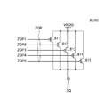
尚、コンパレータ731と741のそれぞれの反転入力端子(−)に入力される抵抗661,662の中点(Vref)の電位は、VDDQの電位が変われば、それに対応して変更されることに注意が必要である。即ち、中点の電位である所定電圧は、電源電圧(VDDQ)が第1の電圧(1.5V)である場合、第1の電圧に対して1/n(抵抗661,662の比)である第1の所定電圧であり、電源電圧(VDDQ)が第2の電圧(1.25V)である場合、第2の電圧に対して前記1/nである第2の所定電圧である。1/nは、例えば1/2である。即ち、nは2であり、この値「2」はJEDECで規格化されたZQ端子を使用したキャリブレーション(出力トランジスタのインピーダンスをマッチングさせるに当たり、出力トランジスタのインピーダンス値とキャリブレーション抵抗(RE)値とをマッチングさせる。)がマッチングしたときのZQ端子の電位(VDDQ/2)の「2」に相当する値である。
Note that the potential of the middle point (Vref) of the
コンパレータ731,741には切替信号SELが入力されており、これによってオフセット電圧の切り替えを行うことができる。具体的には、切替信号SELがハイレベル(VDDQ=VDDQ1)である場合にはオフセット無しに設定され、切替信号SELがローレベル(VDDQ=VDDQ2)である場合にはオフセット有りに設定される。オフセット有りに設定された場合、切替信号SELは、コンパレータ731,741のそれぞれの反転入力端子(−)に入力される電源電圧VDDQが第1の電圧VDDQ1である場合における電源電圧と中間電圧(第1の所定の電圧)の比である第1の比(=1/2)と、電源電圧VDDQが第2の電圧VDDQ2である場合における電源電圧と中間電圧(第2の所定の電圧)の比である第2の比を実質的に互いに異ならせるように、コンパレータ731,741を制御する、つまり第2の比は、≠1/2である。オフセット無しに設定された場合の動作は上述の通りであり、レプリカドライバのインピーダンスが外部抵抗REと一致するよう、キャリブレーション動作が行われる(Ron1=RE)。これに対し、オフセット有りに設定された場合には、レプリカドライバのインピーダンスがRon2(≠RE)である場合を境としてコンパレータ731,741の出力が反転するよう、オフセットが与えられる。これにより、レプリカドライバのインピーダンスがRon2(≠RE)となるよう、キャリブレーション動作が行われることになる。
A switching signal SEL is input to the
このような切り替えを行っているのは、通常のキャリブレーション動作では、インピーダンス目標値が外部抵抗REに固定される一方、本実施形態では、電源電圧VDDQによってインピーダンス目標値が相違するからである。この問題は、図28に示すように、出力ドライバ100を互いに同一インピーダンスに設定される複数の単位ドライバ100aによって構成した場合も同様である。図28に示すように、出力ドライバ100を複数の単位ドライバ100aによって構成し、活性化させる単位ドライバ100aの個数によって出力ドライバ100全体のインピーダンスを切り替える場合、出力ドライバ100全体のインピーダンスは、RE/n(nは1から単位ドライバ100aの個数までの整数)に制限される。この場合、出力ドライバ100のインピーダンスをRon2に設定することができないおそれが生じる。
The reason why such switching is performed is that in the normal calibration operation, the impedance target value is fixed to the external resistor RE, but in the present embodiment, the impedance target value differs depending on the power supply voltage VDDQ. This problem is the same when the
しかしながら、本実施形態では、コンパレータ731,741にオフセットを持たせることによって、インピーダンス目標値の切り替えを可能としていることから、Ron2の値をRE/nで表せない場合であっても、出力ドライバ100のインピーダンスをRon2に設定することが可能となる。また、コンパレータにオフセットを持たせるのではなく、図29に示すキャリブレーション回路700aように、切替信号SELによって基準電位Vrefを変化させる基準電位切替回路760を用い、その出力をコンパレータ631,641に供給することによっても同じ効果を得ることが可能となる。この方法によっても、電源電圧VDDQが第1の電圧VDDQ1である場合における電源電圧と基準電圧Vref(所定の電圧)の比である第1の比と、電源電圧VDDQが第2の電圧VDDQ2である場合における電源電圧と基準電圧Vrefの比である第2の比が互いに相違する。基準電位切替回路760の回路例としては、図30に示すように、VDDQ(電源ライン)及びVSSQ(低電位電源ライン)がそれぞれ供給される複数の電源ライン間に複数の抵抗体(抵抗素子)を直列に接続し、切替信号SELによって分圧の比(分圧比)を切り替え可能とすればよい。
However, in the present embodiment, since the impedance target value can be switched by providing the
詳細には、コンパレータ631と641のそれぞれの反転入力端子(−)に入力される基準電位切替回路760の出力端子(Vref)の電位(所定電圧)は、VDDQの電位が変われば、それに対応して変更されることに注意が必要である。即ち、所定電圧は、電源電圧(VDDQ)が第1の電圧(1.5V)である場合、第1の電圧に対して1/nである第1の所定電圧であり、電源電圧(VDDQ)が第2の電圧(1.25V)である場合、第2の電圧に対して前記1/nと異なる第2の所定電圧である。1/nは、例えば1/2である。図30に示すように、分圧の比(分圧比)を切り替えるとは、前記1/nを変更することに相当する。
Specifically, the potential (predetermined voltage) of the output terminal (Vref) of the reference
以上、本発明の好ましい実施形態について説明したが、本発明は、上記の実施形態に限定されることなく、本発明の主旨を逸脱しない範囲で種々の変更が可能であり、それらも本発明の範囲内に包含されるものであることはいうまでもない。 The preferred embodiments of the present invention have been described above, but the present invention is not limited to the above-described embodiments, and various modifications can be made without departing from the spirit of the present invention. Needless to say, it is included in the range.
例えば、実施形態ではDRAMで開示をしたが、本願の基本的技術思想はこれに限られず、例えば、SRAMやその他の同期型メモリであっても良い。更に、出力ドライバやスルーレート制御回路等の回路形式、その他の制御信号を生成する回路は、上記実施形態によって開示した回路形式に限られない。また、終端抵抗のモデル、終端抵抗が存在する場所も、特に限定されない。 For example, the DRAM is disclosed in the embodiment, but the basic technical idea of the present application is not limited to this, and may be, for example, an SRAM or other synchronous memory. Furthermore, the circuit format such as the output driver and the slew rate control circuit and other circuits that generate control signals are not limited to the circuit format disclosed by the above embodiment. Also, the model of the termination resistor and the location where the termination resistor exists are not particularly limited.
本発明の基本的技術思想は、メモリ機能のシステム以外の半導体装置を使用したシステムにも適用することができる。例えば、CPU(Central Processing Unit)、MCU(Micro Control Unit)、DSP(Digital Signal Processor)、ASIC(Application Specific Integrated Circuit)、ASSP(Application Specific Standard Circuit)等を搭載したシステム全般に、本発明を適用することができる。例えば、本発明の基本的技術思想は、メモリセルの情報を増幅する用途に使用されるデータ信号を処理するバスに限られず、ASIC等のロジックの信号処理、DSP等のデータ信号を処理するバスであっても良い。つまり、本願クレームは、記憶装置の階層バスに限られないことは言うまでもない。マザーボード、モジュール基板の形態は、問わない。システムを構成する個々の半導体装置この構造形態としては、例えば、SOC(システムオンチップ)、MCP(マルチチップパッケージ)やPOP(パッケージオンパッケージ)などが挙げられる。これらの任意の製品形態、パッケージ形態を有する半導体装置に対して本発明を適用することができる。 The basic technical idea of the present invention can be applied to a system using a semiconductor device other than the memory function system. For example, the present invention is applied to all systems equipped with a central processing unit (CPU), a micro control unit (MCU), a digital signal processor (DSP), an application specific integrated circuit (ASIC), an application specific standard circuit (ASSP), and the like. can do. For example, the basic technical idea of the present invention is not limited to a data signal processing bus used for amplifying memory cell information, but a logic signal processing such as an ASIC and a data processing signal such as a DSP. It may be. That is, it goes without saying that the claims of the present application are not limited to the hierarchical bus of the storage device. The form of the mother board and the module board is not limited. Individual semiconductor devices constituting the system Examples of the structure form include SOC (system on chip), MCP (multichip package), and POP (package on package). The present invention can be applied to a semiconductor device having any of these product forms and package forms.
また、トランジスタとして電界効果トランジスタ(Field Effect Transistor; FET)を用い場合には、MOS(Metal Oxide Semiconductor)以外にもMIS(Metal-Insulator Semiconductor)、TFT(Thin Film Transistor)等の様々なFETに適用できる。トランジスタとしては、FET以外のトランジスタ、例えば、バイポーラ型トランジスタであっても良い。 In addition, when a field effect transistor (FET) is used as a transistor, it is applicable to various FETs such as MIS (Metal-Insulator Semiconductor) and TFT (Thin Film Transistor) in addition to MOS (Metal Oxide Semiconductor). it can. The transistor may be a transistor other than an FET, for example, a bipolar transistor.
更に、NMOSトランジスタ(N型チャネルMOSトランジスタ)は、第1導電型のトランジスタ、PMOSトランジスタ(P型チャネルMOSトランジスタ)は、第2導電型のトランジスタの代表例である。 Further, the NMOS transistor (N-type channel MOS transistor) is a representative example of the first conductivity type transistor, and the PMOS transistor (P-type channel MOS transistor) is a representative example of the second conductivity type transistor.
また、本発明の請求の範囲の枠内において種々の開示要素の多様な組み合わせ、ないし選択が可能である。すなわち、本発明は、請求の範囲を含む全開示、技術的思想にしたがって当業者であればなし得るであろう各種変形、修正を含むことは勿論である。 Various combinations and selections of various disclosed elements are possible within the scope of the claims of the present invention. That is, the present invention of course includes various variations and modifications that could be made by those skilled in the art according to the entire disclosure including the claims and the technical idea.
2 マザーボード
4 RDIMM
6 メモリコントローラ
10 DRAM
6a,10a データ入出力端子
12 データ配線
14,14a 出力回路
16 入力回路
18,18a 特性切替回路
20 レジスタチップ
30 AMB
100 出力ドライバ
200 スルーレート制御回路
210,220 スルーレート調整回路
300 スルーレート設定回路
400 ソース電位調整回路
410 レジスタ
420 電圧検出回路
500 出力制御回路
600,700,700a キャリブレーション回路
2
6
6a, 10a Data input /
100
Claims (20)
前記出力ドライバの出力信号の特性を切り替える特性切替回路と、を備え、
前記特性切替回路は、前記出力ドライバの導通時の出力インピーダンスを制御するキャリブレーション回路と、前記出力信号の単位時間あたりの電位遷移量を示すスルーレートを調整するスルーレート制御回路と、を含み、
前記キャリブレーション回路は、前記電源ラインに供給される電源電圧が第1の電圧である場合と前記電源電圧が前記第1の電圧よりも小さい第2の電圧である場合とにおいて、前記第1と第2の電圧にそれぞれ対応する前記出力ドライバの導通時の出力インピーダンスを一致させ、
前記スルーレート制御回路は、
前記第1の電圧である場合には、前記出力信号のスルーレートを相対的に大きくし、且つ前記出力信号の振幅値を前記第1の電圧に対応する第1の振幅値とすることにより、前記出力信号の立ち上がり時間及び立ち下がり時間をそれぞれ第1及び第2の時間とし、
前記電第2の電圧である場合には、前記出力信号のスルーレートを相対的に小さくし、且つ前記出力信号の振幅値を前記第1の振幅値よりも小さい前記第2の電圧に対応する第2の振幅値とすることにより、前記出力信号の立ち上がり時間及び立ち下がり時間をそれぞれ前記第1及び第2の時間とする、ことを特徴とする半導体装置。 An output driver connected to a power line, connected to an external terminal, and outputting an output signal to the external terminal;
A characteristic switching circuit for switching the characteristic of the output signal of the output driver,
The characteristic switching circuit includes a calibration circuit that controls an output impedance when the output driver is conductive, and a slew rate control circuit that adjusts a slew rate indicating a potential transition amount per unit time of the output signal,
In the calibration circuit, the power supply voltage supplied to the power supply line is a first voltage and the power supply voltage is a second voltage smaller than the first voltage. Matching the output impedance when the output driver corresponding to each of the second voltages is conductive;
The slew rate control circuit includes:
In the case of the first voltage, by relatively increasing the slew rate of the output signal and setting the amplitude value of the output signal to the first amplitude value corresponding to the first voltage, The rise time and fall time of the output signal are first and second times, respectively.
In the case of the electric second voltage, the slew rate of the output signal is made relatively small, and the amplitude value of the output signal corresponds to the second voltage smaller than the first amplitude value. The semiconductor device according to claim 1, wherein the second amplitude value is used to set the rise time and the fall time of the output signal as the first time and the second time, respectively.
前記出力ドライバの出力信号の特性を切り替える特性切替回路と、を備え、
前記特性切替回路は、前記出力ドライバの導通時の出力インピーダンスを制御するキャリブレーション回路と、前記出力信号の単位時間あたりの電位遷移量を示すスルーレートを調整するスルーレート制御回路と、を含み、
前記キャリブレーション回路は、前記電源ラインに供給される電源電圧が第1の電圧である場合と前記電源電圧が前記第1の電圧よりも小さい第2の電圧である場合とにおいて、前記第2の電圧に対応する前記出力ドライバの導通時の出力インピーダンスを前記第1の電圧に対応する前記出力ドライバの導通時のインピーダンスよりも低くさせ、
前記スルーレート制御回路は、
前記第1と第2の電圧である場合とにおいて、前記第1と第2の電圧にそれぞれ対応する前記出力信号のスルーレートを一致させ、且つ前記第1と第2の電圧にそれぞれ対応する前記出力信号の第1と第2の振幅値を一致させることにより、
前記第1の電圧である場合における前記出力ドライバの出力信号の立ち上がり時間及び立ち下がり時間をそれぞれ第1及び第2の時間とし、
前記第2の電圧である場合における前記出力ドライバの出力信号の立ち上がり時間及び立ち下がり時間をそれぞれ前記第1及び第2の時間とする、ことを特徴とする半導体装置。 An output driver connected to a power line, connected to an external terminal, and outputting an output signal to the external terminal;
A characteristic switching circuit for switching the characteristic of the output signal of the output driver,
The characteristic switching circuit includes a calibration circuit that controls an output impedance when the output driver is conductive, and a slew rate control circuit that adjusts a slew rate indicating a potential transition amount per unit time of the output signal,
The calibration circuit includes the second power supply circuit when the power supply voltage supplied to the power supply line is a first voltage and when the power supply voltage is a second voltage smaller than the first voltage. An output impedance at the time of conduction of the output driver corresponding to the voltage is made lower than an impedance at the time of conduction of the output driver corresponding to the first voltage;
The slew rate control circuit includes:
In the case of the first and second voltages, the slew rates of the output signals corresponding to the first and second voltages are matched, and the slew rates corresponding to the first and second voltages are respectively matched. By matching the first and second amplitude values of the output signal,
The rise time and fall time of the output signal of the output driver in the case of the first voltage are first and second times, respectively.
A semiconductor device characterized in that a rise time and a fall time of an output signal of the output driver in the case of the second voltage are the first time and the second time, respectively.
Ron2=Ron1(VDDQ2/VDDQ1)−Rtt{1−(VDDQ2/VDDQ1)}
を満足するよう、前記出力ドライバの出力インピーダンスを調整する、ことを特徴とする請求項4に記載の半導体装置。 The first voltage is VDDQ1, the second voltage is VDDQ2, the output impedance when the power supply voltage is the first voltage is Ron1, and the output impedance when the power supply voltage is the second voltage. Ron2, when the resistance value of the termination resistor connected to the output driver is Rtt, the calibration circuit is
Ron2 = Ron1 (VDDQ2 / VDDQ1) −Rtt {1- (VDDQ2 / VDDQ1)}
The semiconductor device according to claim 4, wherein an output impedance of the output driver is adjusted so as to satisfy the following.
前記特性切替回路は、前記出力トランジスタの制御電極に供給する制御信号の電位を調整するソース電位調整回路を含む、ことを特徴とする請求項1乃至6のいずれか一項に記載の半導体装置。 The output driver includes an output transistor connected between the power supply line and an output terminal connected to the external terminal,
The semiconductor device according to claim 1, wherein the characteristic switching circuit includes a source potential adjustment circuit that adjusts a potential of a control signal supplied to a control electrode of the output transistor.
前記電源電圧が前記第1の電圧である場合には前記制御電極に第1の制御電圧を供給し、
前記電源電圧が前記第2の電圧である場合には前記第1の制御電圧を供給した場合よりも前記出力トランジスタに大きな導通電流が得られる第2の制御電圧を前記制御電極に供給することを特徴とする請求項7に記載の半導体装置。 The source potential adjustment circuit includes:
When the power supply voltage is the first voltage, supply a first control voltage to the control electrode;
When the power supply voltage is the second voltage, supplying the control electrode with a second control voltage that provides a larger conduction current to the output transistor than when the first control voltage is supplied. The semiconductor device according to claim 7, characterized in that:
前記出力ドライバと同じ回路構成を有するレプリカドライバと、
前記レプリカドライバの出力電圧を所定の電圧と比較するコンパレータと、
前記コンパレータの出力に基づいて前記レプリカドライバの出力インピーダンスを調整するカウンタと、を含み、
前記出力ドライバの出力インピーダンスが前記カウンタのカウント値によって制御されることを特徴とする請求項4又は5に記載の半導体装置。 The calibration circuit includes:
A replica driver having the same circuit configuration as the output driver;
A comparator that compares the output voltage of the replica driver with a predetermined voltage;
A counter that adjusts the output impedance of the replica driver based on the output of the comparator;
6. The semiconductor device according to claim 4, wherein an output impedance of the output driver is controlled by a count value of the counter.
前記電源電圧が前記第1の電圧である場合における前記第1の電圧と前記第1の所定の電圧の比である第1の比と、前記電源電圧が前記第2の電圧である場合における前記第2の電圧と前記第2の所定の電圧の比である第2の比は、互いに異なる、ことを特徴とする請求項11に記載の半導体装置。 The predetermined voltage is a first predetermined voltage that is 1 / n with respect to the first voltage when the power supply voltage is the first voltage, and the power supply voltage is the second voltage. A second predetermined voltage different from the 1 / n with respect to the second voltage, and the first voltage and the first predetermined voltage when the power supply voltage is the first voltage. A first ratio that is a ratio and a second ratio that is a ratio of the second voltage and the second predetermined voltage when the power supply voltage is the second voltage are different from each other. The semiconductor device according to claim 11, wherein the semiconductor device is characterized in that:
前記特性切替回路は、前記レジスタを参照することによって前記出力ドライバの特性を切り替えることを特徴とする請求項1乃至12のいずれか一項に記載の半導体装置。 A register indicating whether the power supply voltage is the first voltage or the second voltage;
The semiconductor device according to claim 1, wherein the characteristic switching circuit switches the characteristic of the output driver by referring to the register.
前記特性切替回路は、前記電圧検出回路の検出結果を参照することによって前記出力ドライバの特性を切り替える、ことを特徴とする請求項1乃至12のいずれか一項に記載の半導体装置。 A voltage detection circuit for detecting the power supply voltage;
The semiconductor device according to claim 1, wherein the characteristic switching circuit switches characteristics of the output driver by referring to a detection result of the voltage detection circuit.
第2の電源ラインに接続された第1の入力レシーバを有する第2の半導体装置と、
前記第1の出力ドライバが出力する出力信号を前記第1の入力レシーバに伝送するデータ配線と、を備える情報処理システムであって、
前記第1の半導体装置は、前記第1の出力ドライバが出力する出力信号の単位時間あたりの電位遷移量を示すスルーレートを調整する第1のスルーレート制御回路を含み、
前記第1のスルーレート制御回路は、
前記第1の電源ラインに供給される電源電圧が第1の電圧である場合における前記第1の出力ドライバの出力信号の立ち上がり時間及び立ち下がり時間をそれぞれ第1及び第2の時間とし、
前記第1の電源ラインに供給される電源電圧が前記第1の電圧よりも小さい第2の電圧である場合における前記第1の出力ドライバの出力信号の立ち上がり時間及び立ち下がり時間をそれぞれ前記第1及び第2の時間とし、
前記第2電圧に対応する前記第1の出力ドライバの出力信号のスルーレートを前記第1電圧に対応する前記第1の出力ドライバの出力信号のスルーレートよりも小さくし且つ前記第1と第2の電圧にそれぞれ対応する前記第1の出力ドライバのインピーダンスを前記第1と第2の電圧によらず一致させ更に前記第1と第2の電圧にそれぞれ対応する前記第1の出力ドライバの出力信号の振幅値の比を前記第1と第2の電圧との比に対応させるか、または前記第1と2電圧にそれぞれ対応する前記第1の出力ドライバの出力信号のスルーレートを一致させ且つ前記第2の電圧に対応する前記第1の出力ドライバのインピーダンスを前記第1の電圧に対応する前記第1の出力ドライバのインピーダンスよりも低くさせ更に前記第1と第2の電圧にそれぞれ対応する前記第1の出力ドライバの出力信号の振幅値を前記第1と第2の電圧によらず一致させる、ことを特徴とする情報処理システム。 A first semiconductor device having a first output driver connected to a first power supply line;
A second semiconductor device having a first input receiver connected to a second power supply line;
An information processing system comprising: a data line that transmits an output signal output from the first output driver to the first input receiver;
The first semiconductor device includes a first slew rate control circuit that adjusts a slew rate indicating a potential transition amount per unit time of an output signal output from the first output driver,
The first slew rate control circuit includes:
The rise time and fall time of the output signal of the first output driver when the power supply voltage supplied to the first power supply line is the first voltage are set as the first time and the second time, respectively.
The rise time and fall time of the output signal of the first output driver when the power supply voltage supplied to the first power supply line is a second voltage smaller than the first voltage are respectively And the second time,
The slew rate of the output signal of the first output driver corresponding to the second voltage is made smaller than the slew rate of the output signal of the first output driver corresponding to the first voltage, and the first and second The impedance of the first output driver corresponding to each voltage of the first output driver is made to match regardless of the first and second voltages, and the output signal of the first output driver corresponding to the first and second voltages, respectively. The ratio of the amplitude values of the first output driver corresponding to the ratio of the first and second voltages, or the slew rate of the output signal of the first output driver corresponding to the first and second voltages, respectively, and The impedance of the first output driver corresponding to the second voltage is made lower than the impedance of the first output driver corresponding to the first voltage, and the first and second voltages are further reduced. Said first output driver amplitude value of the output signal and the first match regardless of the second voltage and the information processing system characterized the corresponding Re respectively.
前記第2の半導体装置は、前記第2の電源ラインに接続された第2の出力ドライバをさらに有し、
前記データ配線は、前記第2の出力ドライバが出力する出力信号を前記第2の入力レシーバに伝送する双方向の配線である、ことを特徴とする請求項15に記載の情報処理システム。 The first semiconductor device further includes a second input receiver connected to the first power supply line,
The second semiconductor device further includes a second output driver connected to the second power supply line,
The information processing system according to claim 15, wherein the data wiring is a bidirectional wiring that transmits an output signal output from the second output driver to the second input receiver.
前記第2のスルーレート制御回路は、
前記第2の電源ラインに供給される電源電圧が前記第1の電圧である場合における前記第2の出力ドライバの出力信号の立ち上がり時間及び立ち下がり時間をそれぞれ第3及び第4の時間とし、
前記第2の電源ラインに供給される電源電圧が前記第1の電圧よりも小さい第2の電圧である場合における前記第2の出力ドライバの出力信号の立ち上がり時間及び立ち下がり時間をそれぞれ前記第3及び第4の時間とし、
前記第2電圧に対応する前記第2の出力ドライバの出力信号のスルーレートを前記第1電圧に対応する前記第2の出力ドライバの出力信号のスルーレートよりも小さくし且つ前記第1と第2の電圧にそれぞれ対応する前記第2の出力ドライバのインピーダンスを前記第1と第2の電圧によらず一致させ更に前記第1と第2の電圧にそれぞれ対応する前記第2の出力ドライバの出力信号の振幅値の比を前記第1と第2の電圧との比に対応させるか、または前記第1と2電圧にそれぞれ対応する前記第2の出力ドライバの出力信号のスルーレートを一致させ且つ前記第2の電圧に対応する前記第2の出力ドライバのインピーダンスを前記第1の電圧に対応する前記第2の出力ドライバのインピーダンスよりも低くさせ更に前記第1と第2の電圧にそれぞれ対応する前記第2の出力ドライバの出力信号の振幅値を前記第1と第2の電圧によらず一致させる、ことを特徴とする請求項16に記載の情報処理システム。 The second semiconductor device includes a second slew rate control circuit that adjusts a slew rate indicating a potential transition amount per unit time of an output signal output from the second output driver,
The second slew rate control circuit includes:
When the power supply voltage supplied to the second power supply line is the first voltage, the rise time and fall time of the output signal of the second output driver are the third and fourth times, respectively.
When the power supply voltage supplied to the second power supply line is a second voltage smaller than the first voltage, the rise time and fall time of the output signal of the second output driver are respectively set to the third voltage. And the fourth time,
The slew rate of the output signal of the second output driver corresponding to the second voltage is made smaller than the slew rate of the output signal of the second output driver corresponding to the first voltage, and the first and second The impedance of the second output driver corresponding to each voltage of the second output driver is made to match regardless of the first and second voltages, and the output signal of the second output driver corresponding to the first and second voltages, respectively. The ratio of the amplitude value of the second output driver corresponding to the ratio of the first and second voltages, or the slew rate of the output signal of the second output driver corresponding to the first and second voltages, respectively, and The impedance of the second output driver corresponding to the second voltage is made lower than the impedance of the second output driver corresponding to the first voltage, and the first and second voltages are further reduced. The information processing system according to claim 16, wherein the amplitude value of the second output driver of the output signal the first and match regardless of the second voltage, wherein the corresponding Re respectively.
前記出力ドライバに供給される電源電圧が相対的に高い第1の電圧である第1の動作条件と、前記電源電圧が前記第1の電圧よりも相対的に低い第2の電圧である第2の動作条件を有しており、
前記制御回路は、
前記出力ドライバが出力する出力信号の単位時間あたりの電位遷移量を示す前記第2の動作条件におけるスルーレートを、前記第1の動作条件における前記出力ドライバが出力する単位時間あたりの電位遷移量を示すスルーレートよりも小さくさせ、且つ
前記第1の動作条件における前記出力信号の立ち上がり時間及び立ち下がり時間と、前記第2の動作条件における前記出力信号の立ち上がり時間及び立ち下がり時間とをそれぞれ一致させ、且つ
前記第1の動作条件における前記出力ドライバの出力インピーダンスと前記第2の動作条件における前記出力ドライバの出力インピーダンスとを一致させ、更に、
前記第1の動作条件における前記出力信号の振幅値と前記第2の動作条件における前記出力信号の振幅値の比を、前記第1の動作条件における前記電源電圧と前記第2の動作条件における前記電源電圧の比に比例させる、ことを特徴とする情報処理システム。 An information processing system comprising: an output driver; an input receiver that receives an output signal output from the output driver; and a control circuit that controls the output driver;
A first operating condition in which a power supply voltage supplied to the output driver is a relatively high first voltage; and a second operating condition in which the power supply voltage is a second voltage that is relatively lower than the first voltage. Have the following operating conditions:
The control circuit includes:
The slew rate in the second operating condition indicating the amount of potential transition per unit time of the output signal output by the output driver, and the potential transition amount per unit time output by the output driver in the first operating condition. And the rise time and fall time of the output signal under the first operating condition are matched with the rise time and fall time of the output signal under the second operating condition, respectively. And matching the output impedance of the output driver in the first operating condition with the output impedance of the output driver in the second operating condition,
The ratio between the amplitude value of the output signal in the first operating condition and the amplitude value of the output signal in the second operating condition is determined by calculating the ratio between the power supply voltage in the first operating condition and the second operating condition. An information processing system characterized by being proportional to a ratio of power supply voltages.
前記出力ドライバに供給される電源電圧が相対的に高い第1の電圧である第1の動作条件と、前記電源電圧が前記第1の電圧よりも相対的に低い第2の電圧である第2の動作条件を有しており、
前記制御回路は、
前記出力ドライバが出力する出力信号の単位時間あたりの電位遷移量を示す前記第1と第2の動作条件それぞれにおけるスルーレートを一致させ、且つ
前記第1の動作条件における前記出力信号の立ち上がり時間及び立ち下がり時間と、前記第2の動作条件における前記出力信号の立ち上がり時間及び立ち下がり時間とをそれぞれ一致させ、且つ
前記第1の動作条件における前記出力ドライバの出力インピーダンスよりも前記第2の動作条件における前記出力ドライバの出力インピーダンスを低くし、更に
前記第1の動作条件における前記出力信号の振幅値と前記第2の動作条件における前記出力信号の振幅値とを、前記第1と第2の電圧によらず一致させる、ことを特徴とする情報処理システム。 An information processing system comprising: an output driver; an input receiver that receives an output signal output from the output driver; and a control circuit that controls the output driver;
A first operating condition in which a power supply voltage supplied to the output driver is a relatively high first voltage; and a second operating condition in which the power supply voltage is a second voltage that is relatively lower than the first voltage. Have the following operating conditions:
The control circuit includes:
The slew rate in each of the first and second operating conditions indicating the potential transition amount per unit time of the output signal output by the output driver is matched, and the rise time of the output signal in the first operating condition and The second operation condition is made to match the fall time with the rise time and the fall time of the output signal in the second operation condition, and more than the output impedance of the output driver in the first operation condition. The output impedance of the output driver is reduced, and the amplitude value of the output signal under the first operating condition and the amplitude value of the output signal under the second operating condition are expressed as the first and second voltages. An information processing system characterized by matching regardless of whether or not.
Priority Applications (2)
| Application Number | Priority Date | Filing Date | Title |
|---|---|---|---|
| JP2009255568A JP2011101266A (en) | 2009-11-06 | 2009-11-06 | Semiconductor device and information processing system |
| US12/926,255 US8581649B2 (en) | 2009-11-06 | 2010-11-04 | Semiconductor device and information processing system |
Applications Claiming Priority (1)
| Application Number | Priority Date | Filing Date | Title |
|---|---|---|---|
| JP2009255568A JP2011101266A (en) | 2009-11-06 | 2009-11-06 | Semiconductor device and information processing system |
Publications (1)
| Publication Number | Publication Date |
|---|---|
| JP2011101266A true JP2011101266A (en) | 2011-05-19 |
Family
ID=43973707
Family Applications (1)
| Application Number | Title | Priority Date | Filing Date |
|---|---|---|---|
| JP2009255568A Withdrawn JP2011101266A (en) | 2009-11-06 | 2009-11-06 | Semiconductor device and information processing system |
Country Status (2)
| Country | Link |
|---|---|
| US (1) | US8581649B2 (en) |
| JP (1) | JP2011101266A (en) |
Cited By (3)
| Publication number | Priority date | Publication date | Assignee | Title |
|---|---|---|---|---|
| WO2014057546A1 (en) * | 2012-10-10 | 2014-04-17 | 富士通株式会社 | Multi-hit detection circuit, processing device, and multi-hit detection method |
| KR20190029014A (en) * | 2017-09-11 | 2019-03-20 | 에스케이하이닉스 주식회사 | Memory system having impedance calibration circuit |
| KR20190029011A (en) * | 2017-09-11 | 2019-03-20 | 에스케이하이닉스 주식회사 | Memory system having data output driver |
Families Citing this family (16)
| Publication number | Priority date | Publication date | Assignee | Title |
|---|---|---|---|---|
| US7973565B2 (en) * | 2007-05-23 | 2011-07-05 | Cyclos Semiconductor, Inc. | Resonant clock and interconnect architecture for digital devices with multiple clock networks |
| WO2011046987A2 (en) * | 2009-10-12 | 2011-04-21 | Cyclos Semiconductor, Inc. | Resonant clock distribution network architecture for tracking parameter variations in conventional clock distribution networks |
| EP2693640B1 (en) * | 2011-03-31 | 2017-09-13 | Renesas Electronics Corporation | Serial communication device |
| JP2013085078A (en) * | 2011-10-07 | 2013-05-09 | Elpida Memory Inc | Semiconductor device and semiconductor module having the same |
| US8618843B2 (en) * | 2011-12-21 | 2013-12-31 | Ati Technologies Ulc | High speed serial input/output bus voltage mode driver with tunable amplitude and resistance |
| US9391604B2 (en) * | 2012-01-23 | 2016-07-12 | Infineon Technologies Austria Ag | Methods for monitoring functionality of a switch and driver units for switches |
| KR20130096947A (en) * | 2012-02-23 | 2013-09-02 | 삼성전자주식회사 | Memory module having selectively inserted stub resistor corresponding to location of memory device and on-die termination setting method thereof |
| TWI489478B (en) * | 2012-05-07 | 2015-06-21 | Etron Technology Inc | Method of sharing in use an impedance matching circuit of a memory circuit to perform an initial calibration and a full time refresh mode calibration, and memory circuit with an impedance matching circuit capable of being used in an initial calibration a |
| US9048824B2 (en) * | 2012-12-12 | 2015-06-02 | Intel Corporation | Programmable equalization with compensated impedance |
| KR20140123203A (en) * | 2013-04-11 | 2014-10-22 | 삼성전자주식회사 | Memory system |
| US9742406B2 (en) * | 2014-06-12 | 2017-08-22 | Synopsys, Inc. | Circuit skew compensation trigger system |
| US9337807B2 (en) * | 2014-09-30 | 2016-05-10 | Qualcomm Incorporated | Output driver circuit with auto-equalization based on drive strength calibration |
| KR20160148345A (en) * | 2015-06-16 | 2016-12-26 | 에스케이하이닉스 주식회사 | Data output device |
| US10217508B2 (en) | 2016-05-16 | 2019-02-26 | Synopsys, Inc. | SRAM and periphery specialized device sensors |
| US9948300B1 (en) * | 2017-03-20 | 2018-04-17 | Micron Technology, Inc. | Apparatuses and methods for partial bit de-emphasis |
| US11550733B2 (en) * | 2020-07-01 | 2023-01-10 | Arm Limited | Method, system and circuit for managing a secure memory partition |
Family Cites Families (4)
| Publication number | Priority date | Publication date | Assignee | Title |
|---|---|---|---|---|
| US6420913B1 (en) * | 1999-09-20 | 2002-07-16 | Sun Microsystems, Inc. | Dynamic termination logic driver with improved impedance control |
| US6313678B1 (en) * | 1999-10-13 | 2001-11-06 | Texas Instruments Incorporated | Single-pin externally controlled edge rate controller circuit |
| JP4428504B2 (en) * | 2003-04-23 | 2010-03-10 | 株式会社ルネサステクノロジ | Semiconductor integrated circuit device |
| US7425849B2 (en) * | 2004-12-31 | 2008-09-16 | Stmicroelectronics Pvt. Ltd. | Low noise output buffer capable of operating at high speeds |
-
2009
- 2009-11-06 JP JP2009255568A patent/JP2011101266A/en not_active Withdrawn
-
2010
- 2010-11-04 US US12/926,255 patent/US8581649B2/en active Active
Cited By (5)
| Publication number | Priority date | Publication date | Assignee | Title |
|---|---|---|---|---|
| WO2014057546A1 (en) * | 2012-10-10 | 2014-04-17 | 富士通株式会社 | Multi-hit detection circuit, processing device, and multi-hit detection method |
| KR20190029014A (en) * | 2017-09-11 | 2019-03-20 | 에스케이하이닉스 주식회사 | Memory system having impedance calibration circuit |
| KR20190029011A (en) * | 2017-09-11 | 2019-03-20 | 에스케이하이닉스 주식회사 | Memory system having data output driver |
| KR102391503B1 (en) * | 2017-09-11 | 2022-04-28 | 에스케이하이닉스 주식회사 | Memory system having impedance calibration circuit |
| KR102455514B1 (en) * | 2017-09-11 | 2022-10-19 | 에스케이하이닉스 주식회사 | Memory system having data output driver |
Also Published As
| Publication number | Publication date |
|---|---|
| US8581649B2 (en) | 2013-11-12 |
| US20110109361A1 (en) | 2011-05-12 |
Similar Documents
| Publication | Publication Date | Title |
|---|---|---|
| JP2011101266A (en) | Semiconductor device and information processing system | |
| US8531898B2 (en) | On-die termination circuit, data output buffer and semiconductor memory device | |
| US9391612B2 (en) | Output circuit for semiconductor device, semiconductor device having output circuit, and method of adjusting characteristics of output circuit | |
| US9209804B2 (en) | Semiconductor device having impedance calibration function to data output buffer and semiconductor module having the same | |
| US8351292B2 (en) | Semiconductor device and data processing system | |
| US8508251B2 (en) | Semiconductor devices having on-die termination structures for reducing current consumption and termination methods performed in the semiconductor devices | |
| US8674720B2 (en) | Semiconductor device and method of adjusting an impedance of an output buffer | |
| US8766664B2 (en) | Semiconductor device including output circuit constituted of plural unit buffer circuits in which impedance thereof are adjustable | |
| US7495468B2 (en) | Semiconductor memory device with on die termination circuit | |
| CN100466101C (en) | Data output driver | |
| US8476937B2 (en) | Input buffer circuit capable of adjusting variation in skew | |
| JP5584401B2 (en) | Semiconductor device and data processing system including the same | |
| EP1683156B1 (en) | Internal voltage reference for memory interface | |
| EP3203475B1 (en) | Memory interface circuit capable of controlling driving ability and associated control method | |
| US9208877B2 (en) | Semiconductor integrated circuit with data transmitting and receiving circuits | |
| CN111640460B (en) | Terminal resistor circuit and control method thereof | |
| JP2004015804A (en) | Data output driver for minimizing data output timing variation generated by means of data pattern, and data output method | |
| US8618831B2 (en) | Transmitter apparatus, systems, and methods | |
| JP2008228332A (en) | Output circuit of semiconductor device, semiconductor device including the output circuit, and characteristic adjustment method of the output circuit | |
| TW201709205A (en) | Driving circuit | |
| CN116324993A (en) | Low power output driver for power terminals in memory interface applications |
Legal Events
| Date | Code | Title | Description |
|---|---|---|---|
| A300 | Application deemed to be withdrawn because no request for examination was validly filed |
Free format text: JAPANESE INTERMEDIATE CODE: A300 Effective date: 20130108 |