JP2011039905A - Information processing device - Google Patents
Information processing device Download PDFInfo
- Publication number
- JP2011039905A JP2011039905A JP2009188221A JP2009188221A JP2011039905A JP 2011039905 A JP2011039905 A JP 2011039905A JP 2009188221 A JP2009188221 A JP 2009188221A JP 2009188221 A JP2009188221 A JP 2009188221A JP 2011039905 A JP2011039905 A JP 2011039905A
- Authority
- JP
- Japan
- Prior art keywords
- bus
- information processing
- transfer source
- control device
- bus control
- Prior art date
- Legal status (The legal status is an assumption and is not a legal conclusion. Google has not performed a legal analysis and makes no representation as to the accuracy of the status listed.)
- Withdrawn
Links
Images


Classifications
-
- G—PHYSICS
- G06—COMPUTING; CALCULATING OR COUNTING
- G06F—ELECTRIC DIGITAL DATA PROCESSING
- G06F13/00—Interconnection of, or transfer of information or other signals between, memories, input/output devices or central processing units
- G06F13/14—Handling requests for interconnection or transfer
- G06F13/36—Handling requests for interconnection or transfer for access to common bus or bus system
Abstract
Description
本発明は、情報処理装置に関し、特に、オンチップバスのバストラフィックを低減させる技術に関する。 The present invention relates to an information processing apparatus, and more particularly to a technique for reducing bus traffic of an on-chip bus.
従来のオンチップバスでは、時分割制御機構をオンチップバス上に実装したり、オンチップバス内にバッファを持たせたりすることにより、オンチップバス全体におけるバストラフィックを低減させている。(例えば、特許文献1参照) In the conventional on-chip bus, the time-sharing control mechanism is mounted on the on-chip bus, or a buffer is provided in the on-chip bus, thereby reducing bus traffic in the entire on-chip bus. (For example, see Patent Document 1)
従来のオンチップバス構成によるデータは、アクセス頻度、データ属性によってオンチップメモリやSDRAM(Synchronous Dynamic Random Access Memory)へ格納されている。しかし、連続的な処理を各転送元バス制御装置間で共有する際のオンチップバス全体における転送効率を考慮していないため、各転送元バス制御装置間で連続的な処理を実施するためにデータ共有する際、頻繁にメモリへのアクセスが発生する。その結果、オンチップバスのパフォーマンスが低下するおそれがある。 Data according to the conventional on-chip bus configuration is stored in an on-chip memory or SDRAM (Synchronous Dynamic Random Access Memory) according to access frequency and data attributes. However, since the transfer efficiency of the entire on-chip bus when sharing continuous processing among transfer source bus control devices is not considered, in order to perform continuous processing between transfer source bus control devices. When sharing data, access to the memory frequently occurs. As a result, the performance of the on-chip bus may be reduced.
本発明は、かかる点に鑑みてなされたものであり、オンチップバスにおけるメモリへのアクセス回数を少なくすることを課題とする。 The present invention has been made in view of this point, and an object of the present invention is to reduce the number of accesses to a memory on an on-chip bus.
上述した課題を解決するため、本発明によって、次のような手段を講じた。すなわち、複数の転送元バス制御装置と複数の転送先バス制御装置とが階層バスを介してデータを送受信する情報処理装置として、複数の転送元バス制御装置毎に設置された情報保持回路と、複数の情報保持回路を相互に接続可能な専用バスと、複数の転送元バス制御装置毎に設置され、各転送元バス制御装置の接続先として専用バスおよび階層バスのいずれかを選択するバス選択回路と、を備えているものとする。 In order to solve the above-described problems, the present invention has taken the following measures. That is, as an information processing device for transmitting and receiving data via a hierarchical bus between a plurality of transfer source bus control devices and a plurality of transfer destination bus control devices, an information holding circuit installed for each of the plurality of transfer source bus control devices, A dedicated bus that can connect multiple information holding circuits to each other, and a bus selection that is installed for each transfer source bus controller and selects either a dedicated bus or a hierarchical bus as the connection destination of each transfer source bus controller And a circuit.
これによると、階層バスを介してデータを取得し、取得したデータをリングバスを介して順次他の転送元バス制御装置に転送することで、他の転送元バス制御装置が転送先バス制御装置にアクセスする必要がなくなる。これにより、情報処理装置全体において転送先バス制御装置へのアクセス回数を少なくすることができる。 According to this, by acquiring the data via the hierarchical bus and sequentially transferring the acquired data to the other transfer source bus control device via the ring bus, the other transfer source bus control device becomes the transfer destination bus control device. No need to access As a result, the number of accesses to the transfer destination bus control device can be reduced in the entire information processing apparatus.
本発明によると、情報処理装置全体において転送先バス制御装置へのアクセス回数を少なくすることができる。これにより、転送元バス制御装置間における連続した情報処理の効率化、オンチップバスの転送効率の向上及びオンチップバスの面積削減を図ることができる。 According to the present invention, the number of accesses to the transfer destination bus control device can be reduced in the entire information processing apparatus. Thereby, it is possible to improve the efficiency of continuous information processing between the transfer source bus control devices, improve the transfer efficiency of the on-chip bus, and reduce the area of the on-chip bus.
以下、本発明を実施するための形態について、図面を参照しながら説明する。 Hereinafter, embodiments for carrying out the present invention will be described with reference to the drawings.
<第1の実施形態>
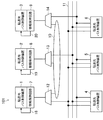
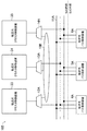
図1は、第1の実施形態に係る情報処理装置100の概略構成を示すブロック図である。図2は、転送元バス制御装置1〜3から発行される制御情報フォーマットである。
<First Embodiment>
FIG. 1 is a block diagram illustrating a schematic configuration of an
情報処理装置100は、複数の転送元バス制御装置1〜3と複数の転送先バス制御装置4〜6との間でデータを送受信する。情報処理装置100は、複数の転送元バス制御装置1〜3毎に設置された情報保持回路7〜9と、情報保持回路7〜9を相互に接続可能なリングバス10と、複数の転送元バス制御装置1〜3と複数の転送先バス制御装置4〜6とを接続可能な階層バス11と、転送元バス制御装置1〜3の出力信号によってリングバス10および階層バス11のいずれかを選択するバス選択回路12〜14と、を備える。
The
上記のように構成された情報処理装置100について、以下にその動作を説明する。まず、転送元バス制御装置1から転送元バス制御装置2、そして転送元バス制御装置3に情報処理が連続して実施される場合を想定する。転送元バス制御装置1は、制御情報のアドレス情報に転送先バス制御装置4を設定して出力する。これにより、バス選択回路12は階層バス11への接続を選択する。転送元バス制御装置1は、転送先バス制御装置4からデータを取得し、情報処理を行う。
The operation of the
情報処理が完了すると、制御情報のアドレス情報に転送先バス制御装置5のアドレス、第一情報処理先に転送元バス制御装置2のアドレス、第二情報処理先に転送元バス制御装置3のアドレスおよび転送情報に処理完了データをそれぞれ設定し、転送先バス制御装置5への転送を開始する。制御情報にアドレス情報を設定している場合、転送元バス制御装置1から転送先バス制御装置5へデータ転送を開始するためバス選択回路12は階層バスへの接続を選択するが、第一情報処理先および第二情報処理先にアドレスが設定してあるため、バス選択回路12はリングバス10への接続を優先して選択し、転送元バス制御装置1は第一情報処理先である転送元バス制御装置2の情報保持回路8へデータ転送を実施する。
When the information processing is completed, the address information of the control destination information is the address of the transfer destination
バス選択回路13,14は、転送元バス制御装置1〜3で連続処理するデータがリングバス10上に存在する場合にリングバス10を優先的に選択する。バス選択回路13は、転送元バス制御装置2からデータの出力要求がない場合に、リングバス10上からデータを受信して情報保持回路8に格納する。
The
転送元バス制御装置2は、処理に必要なデータが情報保持回路8にあるので、転送先バス制御装置5へアクセスせずにデータを取得することができる。転送元バス制御装置2は情報処理を完了すると、制御情報のアドレス情報に転送先バス制御装置6のアドレスおよび転送情報に情報処理完了データを設定するとともに、制御情報の第二情報処理先を第一情報処理先に繰り上げて転送先バス制御装置6へ転送を開始する。しかし、転送元バス制御装置2は、第一情報処理先に転送元バス制御装置3のアドレスを設定したため、第一情報処理先である転送元バス制御装置3の情報保持回路9へデータ転送を実施する。
The transfer source
バス選択回路14は、転送元バス制御装置3からデータの出力要求がない場合に、リングバス10上からデータを受信して情報保持回路9に格納する。転送元バス制御装置3は処理に必要なデータが情報保持回路9にあるので、転送先バス制御装置6へアクセスせずにデータを取得することができる。
The
以上のように、転送先バス制御装置4〜6へのアクセス回数を少なくして情報処理を実施することが可能なので、オンチップバスの転送効率及びSoC(System-on-a-chip)システム性能の向上、オンチップバスの消費電力の削減を図ることができる。
As described above, since it is possible to perform information processing by reducing the number of accesses to the transfer destination
<第2の実施形態>
図3は、第2の実施形態に係る情報処理装置101の概略構成を示すブロック図である。情報処理装置101は、第1の実施形態と同様に図2の制御情報フォーマットを使用する。以下、第1の実施形態との相違点についてのみ説明する。
<Second Embodiment>
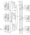
FIG. 3 is a block diagram illustrating a schematic configuration of the
情報処理装置101は、情報保持回路7〜9内にデータが存在することを対応する転送元バス制御装置1〜3に通知する通知バス18〜20を備える。
The
上記のように構成された情報処理装置101について、以下にその動作を説明する。転送元バス制御装置1で情報処理が完了すると、第一情報処理先である転送元バス制御装置2の情報保持回路8へデータ転送を実施する。情報保持回路8へのデータ転送完了次第、情報保持回路8内にデータが存在することを通知バス19を介して転送元バス制御装置2に通知する。転送元バス制御装置2は処理に必要なデータが情報保持回路8にあるので、転送先バス制御装置5へアクセスせずにデータを取得することができる。
The operation of the
転送元バス制御装置2は情報処理を完了すると、制御情報の第二情報処理先を第一情報処理先に繰り上げて、転送元バス制御装置3の情報保持回路9へデータ転送を実施する。情報保持回路9へのデータ転送完了次第、データが情報保持回路9内に存在することを通知バス20を介して転送元バス制御装置3に通知する。転送元バス制御装置3は処理に必要なデータが情報保持回路9にあるので、転送先バス制御装置6へアクセスせずにデータを取得することができる。
When the transfer source
以上のように、情報保持回路7〜9に必要なデータが存在する場合に転送先バス制御装置4〜6にアクセスする必要がなく、情報処理を実施することが可能なので、オンチップバスの転送効率及びSoCシステム性能の向上、オンチップバスの消費電力の削減を図ることができる。
As described above, when necessary data exists in the
<第3の実施形態>
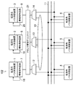
図4は、第3の実施形態に係る情報処理装置102の概略構成を示すブロック図である。情報処理装置102は、図2および図5の制御情報フォーマットを使用する。以下、第2の実施形態との相違点についてのみ説明する。
<Third Embodiment>
FIG. 4 is a block diagram illustrating a schematic configuration of the
情報処理装置102は、転送元バス制御装置1〜3とバス選択回路12〜14との間を通過するデータをモニタするアドレス管理ディレクトリ21を備える。
The
上記のように構成された情報処理装置102について、以下にその動作を説明する。まず、転送元バス制御装置3が転送先バス制御装置4からデータを取得し、さらに転送元バス制御装置1が転送先バス制御装置4からデータを取得する場合を想定する。転送元バス制御装置3は階層バス11を介して転送先バス制御装置4からデータを情報保持回路9内に取得する。
The operation of the
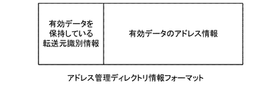
アドレス管理ディレクトリ21は、情報保持回路9に転送先バス制御装置4からデータ取得したという情報を図5の制御情報フォーマットにしたがって管理する。続いて転送元バス制御装置1が転送先バス制御装置4からデータを取得する際、アドレス管理ディレクトリ21は、転送元バス制御装置1が要求するデータが情報保持回路9にあると検出する。アドレス管理ディレクトリ21は、転送元バス制御装置1のアクセス先を転送先バス制御装置4から情報保持回路9に変更するため、図2の制御情報フォーマットにしたがって、第一情報処理先を情報保持回路9に変更する。これにより、バス選択回路12およびバス選択回路14はリングバス10への接続を選択し、転送元バス制御装置1は第一情報処理先である転送元バス制御装置3の情報保持回路9からデータを取得する。
The
<第4の実施形態>
図6は、第4の実施形態に係る情報処理装置103の概略構成を示すブロック図である。情報処理装置103は、図2および図7の制御情報フォーマットを使用する。以下、第2の実施形態との相違点についてのみ説明する。
<Fourth Embodiment>
FIG. 6 is a block diagram illustrating a schematic configuration of the
情報処理装置103は、転送元バス制御装置1〜3のアクセス先情報をモニタする外部アクセスアドレスモニタ22を備える。バス選択回路27〜29は、転送元バス制御装置1〜3の出力信号および外部アクセスアドレスモニタ22の出力信号である選択回路制御信号24〜26によってリングバス10および階層バス11のいずれかを選択する。
The
上記のように構成された情報処理装置103について、以下にその動作を説明する。まず、転送元バス制御装置3が転送先バス制御装置4からデータを取得し、さらに転送元バス制御装置1と転送元バス制御装置2が同時に転送先バス制御装置4からデータを取得する場合を想定する。
The operation of the
転送元バス制御装置3が転送先バス制御装置4からデータを取得するとき、外部アクセスアドレスモニタ22は、転送元バス制御装置3が転送先バス制御装置4からデータ取得中という情報を図7の制御情報フォーマットにしたがって登録する。続いて転送元バス制御装置1および転送元バス制御装置2が転送先バス制御装置4からデータを取得する際、外部アクセスアドレスモニタ22は転送元バス制御装置3がデータ取得中であると検出し、転送元バス制御装置1および転送元バス制御装置2の転送先バス制御装置4へのアクセスを待機状態とする。
When the transfer source
外部アクセスアドレスモニタ22は、選択回路制御信号24〜26を出力する。これにより、バス選択回路27はリングバス10への接続を選択し、バス選択回路28はリングバス10への接続を選択し、バス選択回路29は階層バス11への接続を選択する。転送元バス制御装置3は転送先バス制御装置4からデータを取得し、情報処理を完了する。転送元バス制御装置3の出力信号によってバス選択回路29はリングバス10への接続を選択する。転送元バス制御装置1および転送元バス制御装置2は、リングバス10を介して転送元バス制御装置3の情報保持回路9からデータを取得する。
The external access address monitor 22 outputs selection circuit control signals 24-26. Thereby, the
なお、転送元バス制御装置1および転送元バス制御装置2は、リングバス10からデータを直接取得するようにしてもよい。例えば、外部アクセスアドレスモニタ22に、転送元バス制御装置3が転送先バス制御装置4からデータを取得中であること、および転送元バス制御装置1および転送元バス制御装置2の転送先バス制御装置4へのアクセスが待機状態であることが登録されているとする。この場合、バス選択回路27は選択回路制御信号24を受けると、リングバス10からデータを受信するための入力ポートを接続するとともに、外部アクセスアドレスモニタ22と制御情報を送受するための入出力ポートを接続する。同様に、バス選択回路28は、リングバス10からの入力ポートおよび外部アクセスアドレスモニタ22との入出力ポートをそれぞれ接続する。
Note that the transfer source
バス選択回路29は、選択回路制御信号26を受けると外部アクセスアドレスモニタ22に登録されている制御情報に従って、階層バス11からデータを受信するための入力ポートおよびリングバス10にデータを出力するための出力ポートを接続するとともに、外部アクセスアドレスモニタ22と制御情報を送受するための入出力ポートを接続する。
Upon receiving the selection
バス選択回路27〜29の各ポートが接続されると、転送元バス制御装置3は、転送先バス制御装置4から階層バス11およびバス選択回路29を介してデータを取得する。これとともに、バス選択回路29は、リングバス10にデータを転送する。そして、転送元バス制御装置1および転送元バス制御装置2は、リングバス10からそれぞれバス選択回路27、28を介してデータを取得する。
<第5の実施形態>
図8は、第5の実施形態に係る情報処理装置104の概略構成を示すブロック図である。情報処理装置104は、図2、図5および図7の制御情報フォーマットを使用する。
When the ports of the
<Fifth Embodiment>
FIG. 8 is a block diagram illustrating a schematic configuration of the
情報処理装置104では、第2の実施形態と第3の実施形態と第4の実施形態とを併用する。例えば、転送元バス制御装置1〜3がアドレス管理ディレクトリ21に管理された制御情報に基づいてデータの転送を行う場合には、リングバス10を使用する。一方、外部アクセスアドレスモニタ22に登録された制御情報に基づいてデータの転送を行う場合には、リングバス10Aを使用する。情報処理の併用を実施することにより、各実施の形態で得られる効果を低下させることなく実施可能なので、オンチップバスの転送効率及びSoCシステム性能の向上、オンチップバスの消費電力の削減を図ることができる。なお、リングバスは1つでもよい。
In the
<第6の実施形態>
図9は、第6の実施形態に係る情報処理システム105の概略構成を示すブロック図である。情報処理システム105は、図10の制御情報フォーマットを使用する。
<Sixth Embodiment>
FIG. 9 is a block diagram illustrating a schematic configuration of an
情報処理システム105では、図11に示す転送元クラスタ制御装置33として図8の情報処理装置104を用いる。情報処理システム105は、複数の転送元クラスタ制御装置33〜35と複数の転送先バス制御装置4A〜6Aとが階層バス11Aを介してデータを送受信する。情報処理システム105は、転送元クラスタ制御装置33〜35毎に設置されたクラスタ情報保持回路36と、複数のクラスタ情報保持回路36を相互に接続可能なリングバス10Aと、転送元クラスタ制御装置33〜35の出力信号によってリングバス10Bおよび階層バス11Aのいずれかを選択するバス選択回路12A〜14Aとを備える。
In the
上記のように構成された情報処理システム105において、図2の制御情報フォーマットにクラスタ識別情報を付加した図10の制御情報フォーマットを使用することにより、第1の実施形態と同様の動作をクラスタ単位に拡張して行うことができる。
In the
以上のように、制御情報フォーマットにクラスタ識別情報を付加することにより、SoC内部だけでなくSoC外部にまで拡張可能なので、チップ間の転送効率及びシステム性能の向上、ボード上の消費電力の削減を図ることができる。 As described above, by adding the cluster identification information to the control information format, it can be extended not only inside the SoC but also outside the SoC, thus improving the transfer efficiency between the chips and the system performance, and reducing the power consumption on the board. Can be planned.
なお、上記第1ないし第6の実施形態において、リングバス10,10A,10Bの代わりにメッシュバスを用いてもよい。
In the first to sixth embodiments, a mesh bus may be used instead of the
本発明に係る情報処理装置は、メモリや周辺装置等へのアクセス回数を少なくすることができるため、オンチップバスの転送効率及びSoCシステム性能の向上、消費電力の低下が求められるパソコン等に有用である。 The information processing apparatus according to the present invention can reduce the number of accesses to a memory, a peripheral device, and the like, and thus is useful for personal computers and the like that are required to improve on-chip bus transfer efficiency and SoC system performance and to reduce power consumption. It is.
1〜3 転送元バス制御装置
4〜6,4A〜6A 転送先バス制御装置
7〜9 情報保持回路
10,10A リングバス(専用バス)
10B リングバス(第2の専用バス)
11 階層バス
11A 階層バス(第2の階層バス)
12〜14,12A〜14A バス選択回路
18〜20 通知バス
21 アドレス管理ディレクトリ
22 外部アクセスアドレスモニタ
24〜26 選択回路制御信号
27〜29 バス選択回路
33〜35 転送元クラスタ制御装置
36 クラスタ情報保持回路
100〜105 情報処理装置
1-3 Transfer source bus control device 4-6, 4A-6A Transfer destination bus control device 7-9
10B ring bus (second dedicated bus)
11
12-14, 12A-14A Bus selection circuit 18-20
Claims (9)
前記複数の転送元バス制御装置毎に設置された情報保持回路と、
前記複数の情報保持回路を相互に接続可能な専用バスと、
前記複数の転送元バス制御装置毎に設置され、前記各転送元バス制御装置の接続先として前記専用バスおよび前記階層バスのいずれかを選択するバス選択回路と、を備えている
ことを特徴とする情報処理装置。 An information processing device in which a plurality of transfer source bus control devices and a plurality of transfer destination bus control devices transmit and receive data via a hierarchical bus,
An information holding circuit installed for each of the plurality of transfer source bus control devices;
A dedicated bus capable of interconnecting the plurality of information holding circuits;
A bus selection circuit that is installed for each of the plurality of transfer source bus control devices and that selects either the dedicated bus or the hierarchical bus as a connection destination of the transfer source bus control devices; Information processing apparatus.
前記情報保持回路内にデータが存在することを対応する前記転送元バス制御装置に通知する通知バスを備えている
ことを特徴とする情報処理装置。 The information processing apparatus according to claim 1,
An information processing apparatus, comprising: a notification bus that notifies the corresponding transfer source bus control apparatus that data exists in the information holding circuit.
前記転送元バス制御装置のアクセス先を、前記転送先バス制御装置から前記複数の情報保持回路のうち当該転送元バス制御装置が要求するデータを保持している情報保持回路に変更するアドレス管理ディレクトリを備えている
ことを特徴とする情報処理装置。 The information processing apparatus according to claim 1,
Address management directory for changing the access destination of the transfer source bus control device to an information holding circuit holding data requested by the transfer source bus control device from the transfer destination bus control device among the plurality of information holding circuits An information processing apparatus comprising:
同一のデータを要求する2以上の前記転送元バス制御装置のうち最初に要求する転送元バス制御装置以外の転送元バス制御装置の要求を待機させる外部アクセスアドレスモニタを備え、
前記バス選択回路は、前記外部アクセスアドレスモニタの出力信号によって制御される
ことを特徴とする情報処理装置。 The information processing apparatus according to claim 1,
An external access address monitor that waits for a request from a transfer source bus control device other than the transfer source bus control device that requests first among the two or more transfer source bus control devices that request the same data;
The information processing apparatus, wherein the bus selection circuit is controlled by an output signal of the external access address monitor.
前記専用バスはリングバスである
ことを特徴とする情報処理装置。 The information processing apparatus according to claim 1,
The information processing apparatus, wherein the dedicated bus is a ring bus.
前記専用バスはメッシュバスである
ことを特徴とする情報処理装置。 The information processing apparatus according to claim 1,
The information processing apparatus, wherein the dedicated bus is a mesh bus.
前記転送元クラスタ制御装置毎に設置されたクラスタ情報保持回路と、
前記複数のクラスタ情報保持回路を相互に接続可能な第2の専用バスと、
前記転送元クラスタ制御装置毎に設置され、前記各転送元クラスタ制御装置の接続先として前記第2の階層バスおよび前記第2の専用バスのいずれかを選択するバス選択回路と、を備えている
ことを特徴とする情報処理システム。 An information processing system in which the information processing device according to claim 1 as a plurality of transfer source cluster control devices and a plurality of transfer destination bus control devices transmit and receive data via a second hierarchical bus,
A cluster information holding circuit installed for each transfer source cluster controller;
A second dedicated bus capable of interconnecting the plurality of cluster information holding circuits;
A bus selection circuit which is installed for each transfer source cluster control device and selects either the second hierarchical bus or the second dedicated bus as a connection destination of each transfer source cluster control device; An information processing system characterized by this.
前記第2の専用バスはリングバスである
ことを特徴とする情報処理システム。 The information processing system according to claim 7,
The information processing system, wherein the second dedicated bus is a ring bus.
前記第2の専用バスはメッシュバスである
ことを特徴とする情報処理システム。 The information processing system according to claim 7,
The information processing system, wherein the second dedicated bus is a mesh bus.
Priority Applications (3)
| Application Number | Priority Date | Filing Date | Title |
|---|---|---|---|
| JP2009188221A JP2011039905A (en) | 2009-08-17 | 2009-08-17 | Information processing device |
| PCT/JP2010/000635 WO2011021312A1 (en) | 2009-08-17 | 2010-02-03 | Information processing device |
| US13/367,960 US20120137039A1 (en) | 2009-08-17 | 2012-02-07 | Information processing apparatus |
Applications Claiming Priority (1)
| Application Number | Priority Date | Filing Date | Title |
|---|---|---|---|
| JP2009188221A JP2011039905A (en) | 2009-08-17 | 2009-08-17 | Information processing device |
Publications (2)
| Publication Number | Publication Date |
|---|---|
| JP2011039905A true JP2011039905A (en) | 2011-02-24 |
| JP2011039905A5 JP2011039905A5 (en) | 2012-07-19 |
Family
ID=43606774
Family Applications (1)
| Application Number | Title | Priority Date | Filing Date |
|---|---|---|---|
| JP2009188221A Withdrawn JP2011039905A (en) | 2009-08-17 | 2009-08-17 | Information processing device |
Country Status (3)
| Country | Link |
|---|---|
| US (1) | US20120137039A1 (en) |
| JP (1) | JP2011039905A (en) |
| WO (1) | WO2011021312A1 (en) |
Families Citing this family (1)
| Publication number | Priority date | Publication date | Assignee | Title |
|---|---|---|---|---|
| KR102012699B1 (en) | 2013-01-25 | 2019-08-21 | 삼성전자 주식회사 | Multi bus system and semiconductor system comprising thereof |
Family Cites Families (12)
| Publication number | Priority date | Publication date | Assignee | Title |
|---|---|---|---|---|
| JPH04135268A (en) * | 1990-08-03 | 1992-05-08 | Mitsubishi Electric Corp | Multi-cpu system |
| JPH07235772A (en) * | 1994-02-25 | 1995-09-05 | Fujitsu Ltd | Thin-film multilayer circuit board and production therefor |
| US5754803A (en) * | 1996-06-27 | 1998-05-19 | Interdigital Technology Corporation | Parallel packetized intermodule arbitrated high speed control and data bus |
| US6804527B2 (en) * | 2001-01-19 | 2004-10-12 | Raze Technologies, Inc. | System for coordination of TDD transmission bursts within and between cells in a wireless access system and method of operation |
| US7085866B1 (en) * | 2002-02-19 | 2006-08-01 | Hobson Richard F | Hierarchical bus structure and memory access protocol for multiprocessor systems |
| US7051135B2 (en) * | 2002-11-22 | 2006-05-23 | Ess Technology, Inc. | Hierarchical bus arbitration |
| US7254658B2 (en) * | 2004-06-08 | 2007-08-07 | Arm Limited | Write transaction interleaving |
| US7350002B2 (en) * | 2004-12-09 | 2008-03-25 | Agere Systems, Inc. | Round-robin bus protocol |
| JP2007241918A (en) * | 2006-03-13 | 2007-09-20 | Fujitsu Ltd | Processor device |
| KR20080074545A (en) * | 2007-02-09 | 2008-08-13 | 삼성전자주식회사 | Bus system and control method thereof |
| JP2009003633A (en) * | 2007-06-20 | 2009-01-08 | Panasonic Corp | Information processor |
| US7886096B2 (en) * | 2008-08-08 | 2011-02-08 | Texas Instruments Incorporated | Throughput measurement of a total number of data bits communicated during a communication period |
-
2009
- 2009-08-17 JP JP2009188221A patent/JP2011039905A/en not_active Withdrawn
-
2010
- 2010-02-03 WO PCT/JP2010/000635 patent/WO2011021312A1/en active Application Filing
-
2012
- 2012-02-07 US US13/367,960 patent/US20120137039A1/en not_active Abandoned
Also Published As
| Publication number | Publication date |
|---|---|
| US20120137039A1 (en) | 2012-05-31 |
| WO2011021312A1 (en) | 2011-02-24 |
Similar Documents
| Publication | Publication Date | Title |
|---|---|---|
| KR101720134B1 (en) | Bus bridge apparatus | |
| JP2015531524A (en) | Memory access control module and related method | |
| RU2625558C2 (en) | Architecture of on-chip interconnections | |
| KR20110122516A (en) | Interconnect, bus system having interconnect and operating method of bus system | |
| US20100328216A1 (en) | Information processing apparatus and input control method | |
| WO2012167566A1 (en) | Route switching device, network switching system and route switching method | |
| KR20160046883A (en) | Mesh performance improvement using dual voltage data transfer | |
| US20190286606A1 (en) | Network-on-chip and computer system including the same | |
| WO2011021312A1 (en) | Information processing device | |
| CN102662886A (en) | Optimization method of SoC (System on Chip) address mapping | |
| US9672168B2 (en) | System interconnection of system-on-chip | |
| JP2018517961A (en) | Shared control of phase-locked loop (PLL) for multiport physical layer (PHY) | |
| KR20210001907A (en) | Data transmission apparatuses, data processing systems and methods, and media | |
| JP2009003633A (en) | Information processor | |
| JP2005250653A (en) | Multilayer system and clock controlling method | |
| JP2007213411A (en) | Bus bridge device | |
| JP2011039905A5 (en) | ||
| KR20050064568A (en) | On-chip serialized peripheral bus system and operating method thereof | |
| JP2011113516A (en) | Lsi chip lamination system | |
| JP3959407B2 (en) | Image processing apparatus and image processing system | |
| JP2010033314A (en) | Bus access circuit device and bus access method | |
| US8407385B2 (en) | Bus arbitration system, a method of connecting devices of an IC employing a bus system and an IC | |
| KR20080028064A (en) | Apparatus for extending memory in communication system | |
| JP2001014270A (en) | Data transfer method and device and their application system | |
| JP2002342265A (en) | Computer system using multiplexed path |
Legal Events
| Date | Code | Title | Description |
|---|---|---|---|
| A521 | Written amendment |
Free format text: JAPANESE INTERMEDIATE CODE: A523 Effective date: 20120601 |
|
| A621 | Written request for application examination |
Free format text: JAPANESE INTERMEDIATE CODE: A621 Effective date: 20120601 |
|
| RD02 | Notification of acceptance of power of attorney |
Free format text: JAPANESE INTERMEDIATE CODE: A7422 Effective date: 20120601 |
|
| A761 | Written withdrawal of application |
Free format text: JAPANESE INTERMEDIATE CODE: A761 Effective date: 20121001 |