JP2011022860A - Biometric authentication apparatus - Google Patents
Biometric authentication apparatus Download PDFInfo
- Publication number
- JP2011022860A JP2011022860A JP2009168095A JP2009168095A JP2011022860A JP 2011022860 A JP2011022860 A JP 2011022860A JP 2009168095 A JP2009168095 A JP 2009168095A JP 2009168095 A JP2009168095 A JP 2009168095A JP 2011022860 A JP2011022860 A JP 2011022860A
- Authority
- JP
- Japan
- Prior art keywords
- light
- microlens array
- biometric authentication
- authentication
- authentication device
- Prior art date
- Legal status (The legal status is an assumption and is not a legal conclusion. Google has not performed a legal analysis and makes no representation as to the accuracy of the status listed.)
- Pending
Links
- 238000003384 imaging method Methods 0.000 claims abstract description 58
- 239000000463 material Substances 0.000 claims abstract description 26
- 230000003287 optical effect Effects 0.000 claims description 8
- 229920005989 resin Polymers 0.000 claims description 7
- 239000011347 resin Substances 0.000 claims description 7
- 229920005992 thermoplastic resin Polymers 0.000 claims description 7
- 230000007246 mechanism Effects 0.000 claims description 5
- 238000001514 detection method Methods 0.000 abstract description 11
- 238000004040 coloring Methods 0.000 abstract description 6
- 230000002093 peripheral effect Effects 0.000 description 19
- 230000005540 biological transmission Effects 0.000 description 16
- 210000003462 vein Anatomy 0.000 description 14
- 238000000034 method Methods 0.000 description 13
- 230000006870 function Effects 0.000 description 10
- 238000010586 diagram Methods 0.000 description 4
- 239000007769 metal material Substances 0.000 description 4
- 239000002861 polymer material Substances 0.000 description 4
- XECAHXYUAAWDEL-UHFFFAOYSA-N acrylonitrile butadiene styrene Chemical compound C=CC=C.C=CC#N.C=CC1=CC=CC=C1 XECAHXYUAAWDEL-UHFFFAOYSA-N 0.000 description 3
- 239000004676 acrylonitrile butadiene styrene Substances 0.000 description 3
- 229920000122 acrylonitrile butadiene styrene Polymers 0.000 description 3
- -1 for example Chemical compound 0.000 description 3
- 239000011159 matrix material Substances 0.000 description 3
- 229920000106 Liquid crystal polymer Polymers 0.000 description 2
- 239000004977 Liquid-crystal polymers (LCPs) Substances 0.000 description 2
- 239000004734 Polyphenylene sulfide Substances 0.000 description 2
- 239000003086 colorant Substances 0.000 description 2
- 230000000694 effects Effects 0.000 description 2
- 238000001746 injection moulding Methods 0.000 description 2
- 238000004519 manufacturing process Methods 0.000 description 2
- 238000000465 moulding Methods 0.000 description 2
- 229920000069 polyphenylene sulfide Polymers 0.000 description 2
- 230000009467 reduction Effects 0.000 description 2
- 238000002834 transmittance Methods 0.000 description 2
- 239000004925 Acrylic resin Substances 0.000 description 1
- 229920000178 Acrylic resin Polymers 0.000 description 1
- 102000001554 Hemoglobins Human genes 0.000 description 1
- 108010054147 Hemoglobins Proteins 0.000 description 1
- 238000010521 absorption reaction Methods 0.000 description 1
- NIXOWILDQLNWCW-UHFFFAOYSA-N acrylic acid group Chemical group C(C=C)(=O)O NIXOWILDQLNWCW-UHFFFAOYSA-N 0.000 description 1
- 230000009471 action Effects 0.000 description 1
- 239000001000 anthraquinone dye Substances 0.000 description 1
- 230000000903 blocking effect Effects 0.000 description 1
- 239000008280 blood Substances 0.000 description 1
- 210000004369 blood Anatomy 0.000 description 1
- 230000015556 catabolic process Effects 0.000 description 1
- 230000000295 complement effect Effects 0.000 description 1
- 239000000470 constituent Substances 0.000 description 1
- 239000006059 cover glass Substances 0.000 description 1
- 150000001925 cycloalkenes Chemical class 0.000 description 1
- 238000006731 degradation reaction Methods 0.000 description 1
- 238000009826 distribution Methods 0.000 description 1
- 239000000975 dye Substances 0.000 description 1
- 229910052500 inorganic mineral Inorganic materials 0.000 description 1
- 238000003475 lamination Methods 0.000 description 1
- 229910044991 metal oxide Inorganic materials 0.000 description 1
- 150000004706 metal oxides Chemical class 0.000 description 1
- 239000011707 mineral Substances 0.000 description 1
- 238000012986 modification Methods 0.000 description 1
- 230000004048 modification Effects 0.000 description 1
- 150000002894 organic compounds Chemical class 0.000 description 1
- 239000000049 pigment Substances 0.000 description 1
- 229920003229 poly(methyl methacrylate) Polymers 0.000 description 1
- 239000004417 polycarbonate Substances 0.000 description 1
- 229920000515 polycarbonate Polymers 0.000 description 1
- 239000004926 polymethyl methacrylate Substances 0.000 description 1
- 229920000098 polyolefin Polymers 0.000 description 1
- 230000008569 process Effects 0.000 description 1
- 239000004065 semiconductor Substances 0.000 description 1
- 229920001169 thermoplastic Polymers 0.000 description 1
- 239000004416 thermosoftening plastic Substances 0.000 description 1
Images


Classifications
-
- G—PHYSICS
- G06—COMPUTING; CALCULATING OR COUNTING
- G06V—IMAGE OR VIDEO RECOGNITION OR UNDERSTANDING
- G06V40/00—Recognition of biometric, human-related or animal-related patterns in image or video data
- G06V40/10—Human or animal bodies, e.g. vehicle occupants or pedestrians; Body parts, e.g. hands
- G06V40/12—Fingerprints or palmprints
- G06V40/13—Sensors therefor
- G06V40/1318—Sensors therefor using electro-optical elements or layers, e.g. electroluminescent sensing
-
- H—ELECTRICITY
- H01—ELECTRIC ELEMENTS
- H01L—SEMICONDUCTOR DEVICES NOT COVERED BY CLASS H10
- H01L27/00—Devices consisting of a plurality of semiconductor or other solid-state components formed in or on a common substrate
- H01L27/14—Devices consisting of a plurality of semiconductor or other solid-state components formed in or on a common substrate including semiconductor components sensitive to infrared radiation, light, electromagnetic radiation of shorter wavelength or corpuscular radiation and specially adapted either for the conversion of the energy of such radiation into electrical energy or for the control of electrical energy by such radiation
- H01L27/144—Devices controlled by radiation
- H01L27/146—Imager structures
- H01L27/14601—Structural or functional details thereof
- H01L27/14625—Optical elements or arrangements associated with the device
- H01L27/14627—Microlenses
-
- G—PHYSICS
- G06—COMPUTING; CALCULATING OR COUNTING
- G06V—IMAGE OR VIDEO RECOGNITION OR UNDERSTANDING
- G06V40/00—Recognition of biometric, human-related or animal-related patterns in image or video data
- G06V40/10—Human or animal bodies, e.g. vehicle occupants or pedestrians; Body parts, e.g. hands
- G06V40/12—Fingerprints or palmprints
- G06V40/1341—Sensing with light passing through the finger
-
- G—PHYSICS
- G06—COMPUTING; CALCULATING OR COUNTING
- G06V—IMAGE OR VIDEO RECOGNITION OR UNDERSTANDING
- G06V40/00—Recognition of biometric, human-related or animal-related patterns in image or video data
- G06V40/10—Human or animal bodies, e.g. vehicle occupants or pedestrians; Body parts, e.g. hands
- G06V40/14—Vascular patterns
Landscapes
- Engineering & Computer Science (AREA)
- Physics & Mathematics (AREA)
- General Physics & Mathematics (AREA)
- Power Engineering (AREA)
- Computer Hardware Design (AREA)
- Condensed Matter Physics & Semiconductors (AREA)
- Electromagnetism (AREA)
- Microelectronics & Electronic Packaging (AREA)
- Human Computer Interaction (AREA)
- Multimedia (AREA)
- Theoretical Computer Science (AREA)
- Measurement Of The Respiration, Hearing Ability, Form, And Blood Characteristics Of Living Organisms (AREA)
- Image Input (AREA)
Abstract
Description
本発明は、静脈や指紋などの生体部位における構造物を撮像して得られたデータに基づいて生体の認証を行う生体認証装置に関する。 The present invention relates to a biometric authentication device that performs biometric authentication based on data obtained by imaging a structure in a biological part such as a vein or a fingerprint.
従来、生体部位における構造物を撮像対象とする撮像装置は、生体認証装置等に利用され、例えば指紋や静脈の撮像データを用いて生体の認証を行う認証装置が種々提案されている。一般に、このような生体認証装置では、撮像装置自体の厚みが大きいため、薄型の機器に応用するために、撮像装置を認証装置の外部に配置したり、あるいは撮像装置の光学系(撮像レンズ)と検出系(撮像素子)とを独立して配置することが主流となっていた。 2. Description of the Related Art Conventionally, an imaging apparatus that captures a structure in a biological part as an imaging target is used in a biometric authentication apparatus or the like. For example, various authentication apparatuses that perform biometric authentication using fingerprint or vein imaging data have been proposed. In general, in such a biometric authentication device, since the imaging device itself is thick, the imaging device is arranged outside the authentication device or applied to an optical device (imaging lens) for application to a thin device. And the detection system (imaging device) are arranged independently.
ところが、近年では、様々な機器の薄型化、あるいは製造性やデザインの制約等に伴い、そのような機器に直接搭載することのできるモジュールとして、撮像光学系にマイクロレンズアレイを用いた生体認証装置が提案されている(例えば、特許文献1,2)。
However, in recent years, biometric authentication devices using a microlens array in an imaging optical system as a module that can be directly mounted on various devices due to thinning of various devices or restrictions on manufacturability and design. Has been proposed (for example,
ここで、例えば静脈のパターンを用いて生体認証を行う場合、血中に含まれるヘモグロビンが近赤外光を吸収するという性質を利用して撮像データを取得する。このため、生体部位を照明する光源としては、近赤外光を発するLED(Light Emitting Diode)等が用いられている。ところが、その際、撮像素子において、認証に必要な近赤外光の他に、蛍光灯や白熱灯あるいは太陽光等の認証に不要な外光までもが受光されることがあり、この外光の影響によって、認証精度が低下してしまうという問題がある。 Here, for example, when biometric authentication is performed using a vein pattern, imaging data is acquired using the property that hemoglobin contained in blood absorbs near-infrared light. For this reason, as a light source for illuminating a living body part, an LED (Light Emitting Diode) that emits near infrared light or the like is used. However, in that case, the image sensor may receive not only near-infrared light necessary for authentication but also external light unnecessary for authentication such as fluorescent light, incandescent light, and sunlight. As a result, there is a problem that the authentication accuracy is degraded.
そこで、上記特許文献2にも記載されているように、可視光を遮断して近赤外光を選択的に透過させる波長選択フィルタを併設することが多い。しかしながら、このような波長選択フィルタを用いた場合、認証精度を高めることはできるものの、装置全体の厚みが増してしまうという問題があり、機器の更なる薄型化への対応が困難となる。
Therefore, as described in
本発明はかかる問題点に鑑みてなされたもので、その目的は、高い認証精度を保持しつつ、薄型化を実現することが可能な生体認証装置を提供することにある。 The present invention has been made in view of such problems, and an object of the present invention is to provide a biometric authentication apparatus capable of realizing a reduction in thickness while maintaining high authentication accuracy.
本発明の生体認証装置は、生体に向けて認証用の波長域を含む波長域の光を出射する光源と、生体からの光を集光すると共に、認証用の波長域の光を選択的に透過させるマイクロレンズアレイと、マイクロレンズアレイによって集光された光に基づき、生体の撮像データを取得する撮像素子と、撮像素子で取得された撮像データに基づいて生体の認証を行う認証部とを備えたものである。 The biometric authentication device of the present invention selectively emits light in a wavelength range for authentication and a light source that emits light in a wavelength range including a wavelength range for authentication toward a living body and light from the living body. A microlens array to be transmitted; an imaging element that acquires imaging data of a living body based on light collected by the microlens array; and an authentication unit that authenticates the living body based on imaging data acquired by the imaging element. It is provided.
本発明の生体認証装置では、光源により生体が照明されると、マイクロレンズアレイにおいて、認証用の波長域の光が選択的に透過され、この透過光が撮像素子において受光される。撮像素子では、受光した認証用の波長域の光に基づく撮像データが得られ、認証部は、その撮像データに基づいて生体の認証を行う。 In the biometric authentication device of the present invention, when the living body is illuminated by the light source, light in the wavelength region for authentication is selectively transmitted through the microlens array, and this transmitted light is received by the imaging device. The imaging device obtains imaging data based on the received light in the wavelength region for authentication, and the authentication unit authenticates the living body based on the imaging data.
本発明の生体認証装置によれば、生体からの光を集光するマイクロレンズアレイが、認証用の波長域の光を選択的に透過させるようにしたので、認証用の波長域の光に基づいて、生体の撮像データを取得することができる。すなわち、マイクロレンズアレイが、集光機能と共に、波長選択透過機能を有するので、認証に不要な波長域の光を排除して、認証に必要な波長域の光に基づく撮像データを得ることができる。従って、装置内に波長選択透過フィルタを別途設ける必要がない。よって、高い認証精度を保持しつつ薄型化を実現可能となる。 According to the biometric authentication device of the present invention, since the microlens array that collects light from the living body selectively transmits light in the wavelength region for authentication, it is based on light in the wavelength region for authentication. Thus, imaging data of the living body can be acquired. That is, since the microlens array has a wavelength selective transmission function as well as a condensing function, it is possible to obtain imaging data based on light in a wavelength range necessary for authentication by eliminating light in a wavelength range unnecessary for authentication. . Therefore, it is not necessary to separately provide a wavelength selective transmission filter in the apparatus. Therefore, it is possible to reduce the thickness while maintaining high authentication accuracy.
以下の順に本発明の実施の形態について、図面を参照して詳細に説明する。
(1)全体構成
(2)組み立て方法
Embodiments of the present invention will be described in detail in the following order with reference to the drawings.
(1) Overall configuration (2) Assembly method
(1)全体構成
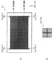
図1は、本発明の一実施の形態に係る生体認証装置1の全体構成を表すものである。図2は、生体認証装置1のZ−X断面構成を表すものである。生体認証装置1は、特に生体(例えば、指先)2の構造物、例えば静脈を撮像して認証を行うものである。この生体認証装置1は、光源10と、検知部11と、マイクロレンズアレイ12と、遮光部13と、撮像素子14と、画像処理部15と、パターン保持部16と、認証部17と、光源駆動部181と、撮像素子駆動部182と、制御部19とから構成されている。
(1) Overall Configuration FIG. 1 shows the overall configuration of a
光源10は、撮像対象である生体2へ向けて光を照射するものであり、例えば、LEDなどにより構成される。この光源10は、例えば、生体2に対して撮像素子14と同一の側に、例えば生体2の長手方向(X方向)における両端位置に設けられている。この光源10は、生体2の内部の構造物、例えば静脈を撮像する場合には、近赤外光の波長領域(700nm〜1200nm程度の波長領域)の光を発するようになっている。
The
検知部11は、例えばカバーガラスなどであり、生体2を検知する領域(面)、すなわち生体2が置かれる領域(面)である。但し、検知部11に直接、生体2が接触している必要はなく、検知部11の上方に生体2が配置されるような構成であればよい。
The
マイクロレンズアレイ12は、例えば検知部11の下方において、生体2内部の観察面を撮像素子14上の受光面に結像するように配置され、生体2に照射された光を集光するようになっている。このマイクロレンズアレイ12は、例えばシクロオレフィン系、ポリオレフィン系またはポリカーボネート系などの熱可塑性の透明樹脂材料を母材(第1の樹脂層)として、顔料、染料などの着色材(遮光材)を添加し、例えば射出成型によって形成される。この際、着色材として、例えば可視光を遮断する有機化合物や天然鉱物などを熱可塑性樹脂(母材)に練りこむことによって、マイクロレンズアレイ12は、例えば図3に示したように700nm以下の波長領域の光を遮断する波長選択透過機能が備わる。言い換えると、このマイクロレンズアレイ12は、認証に用いる光源10の波長領域(近赤外光の波長領域)の光を選択的に透過させる機能を備えている。ここで、着色材としては、成型後のマイクロレンズアレイ12において用いられる波長領域での透過率特性および複屈折特性等の光学特性を考慮して選択するようにする。
The
このようにして成型されたマイクロレンズアレイ12は、図4(A),(B)に示したように、複数のマイクロレンズ12Cがマトリクス状に隙間なく敷き詰められた矩形状のレンズ領域12Aと、周辺領域12Bとを有している。この周辺領域12Bでは、レンズ領域12Aにおける矩形状の各辺の中央部分に、開口部12a〜12dがそれぞれ設けられている。加えて、周辺領域12Bにおけるレンズ領域12Aの各長辺の両端に対応する位置には、貫通孔12e〜12hまたはマイクロレンズ12i〜12lが形成されている。
As shown in FIGS. 4A and 4B, the
遮光部13における遮光部分は、マイクロレンズアレイ12において隣接するマイクロレンズ12C間の境界領域にそれぞれ設けられている。言い換えると、遮光部13には、複数のマイクロレンズ12Cのそれぞれに対応して開口13Cが設けられている。この遮光部13は、マイクロレンズアレイ12への入射光線もしくはマイクロレンズアレイ12からの出射光線を選択的な領域で遮光することにより、撮像素子14側への入射光線を制限するようになっている。ここでは、遮光部13は、近赤外光を遮光する材料、例えばABS(アクリロニトリルブタジエンスチレン)を母材(第2の樹脂層)として、これにマイクロレンズアレイ12と同様に着色材を添加し、射出成型によって形成される。この際、着色材として、高分子材料や金属材料などの光機能材料を熱可塑性樹脂(母材)に練りこむことによって、遮光部13は、近赤外光に加えて可視光に対する遮光機能が追加されるようになっている。ここで、着色材としては、良好な成型特性を有する不透明な材料を選択するようにする。なお、遮光部13の母材としては、上記したABSの他に、例えば、PMMA(アクリル)、PPS(ポリフェニレンスルファイド)またはLCP(液晶ポリマー)などを用いてもよい。
The light shielding portion in the
このようにして成形された遮光部13は、図5(A),(B)に示したように、遮光領域13Aと、周辺領域13Bとを有している。この周辺領域13Bでは、前述したマイクロレンズアレイ12における開口部12a〜12dに対向する位置に、突起部13a〜13dがそれぞれ設けられている。加えて、マイクロレンズアレイ12における貫通孔12e〜12hもしくはマイクロレンズ12i〜12lに対向する位置には、貫通孔13e〜13hがそれぞれ形成されている。
As shown in FIGS. 5A and 5B, the
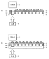
撮像素子14は、マイクロレンズアレイ12からの光を受光して撮像データを取得するものであり、マイクロレンズアレイ12の焦点面に配置されるようになっている。この撮像素子14は、例えば、マトリクス状に配列された複数のCCD(Charge Coupled Device;電荷結合素子)やCMOS(Complementary Metal Oxide Semiconductor)などにより構成される。また、撮像素子14は、マイクロレンズアレイ12および遮光部13と同様に、図6(A)に示したように、撮像素子領域14Aと周辺領域14Bとを有している。この周辺領域14Bでは、前述したマイクロレンズアレイ12および遮光部13の周辺領域12B,13Bにおける貫通孔12e〜12h(もしくはマイクロレンズ12i〜12l)および貫通孔13e〜13hに対向する位置に、アライメントマーク14a〜14dがそれぞれ設けられている。図6(B)は、これらのアライメントマーク14a〜14dの一例を拡大して示したものであるが、この形状に限定されるものではなく、他の形状のものを用いるようにしてもよい。
The
画像処理部15は、制御部19からの制御に応じて、撮像素子14で得られた撮像データに所定の画像処理を施し、認証部17へ出力するものである。なお、この画像処理部15、ならびに後述する認証部17および制御部19は、例えばマイクロコンピュータなどにより構成される。
The
パターン保持部16は、生体認証の際に用いる生体認証パターン(認証の際に撮像して得られた撮像パターンに対する比較パターンであり、予め生体を撮像して得られたもの)が保持される部分である。このパターン保持部16は、不揮発性の記録素子(例えば、EEPROM(Electrically Erasable Programmable Read Only Memory)など)により構成される。
The
認証部17は、制御部19からの制御に応じて、画像処理部15から出力される撮像パターンと、パターン保持部16に保持されている生体認証パターンとを比較することにより、生体2の認証を行う部分である。
The
光源駆動部181は、制御部19からの制御に応じて、光源10の発光駆動を行うものである。撮像素子駆動部182は、制御部19からの制御に応じて、撮像素子13の撮像駆動(受光駆動)を行うものである。制御部19は、画像処理部15、認証部17、光源駆動部181および撮像素子駆動部182の動作を制御するものである。
The light
次に、図7(A),(B)を参照して、これまで説明したマイクロレンズアレイ12、遮光部13および撮像素子14同士の組み立て方法(積層方法)について説明する。
Next, with reference to FIGS. 7A and 7B, the assembly method (lamination method) of the
(2)組み立て方法
マイクロレンズアレイ12の周辺領域12Bには、以下説明する組み立ての際の位置合わせ機構として、上述したように、開口部12a〜12dと、貫通孔12e〜12hあるいはマイクロレンズ12i〜12lとが形成されている。同様に遮光部13の周辺領域13Bには、位置合わせ機構として、突起部13a〜13dおよび貫通孔13e〜13hが形成されている。また、撮像素子14周辺領域14Bには、位置合わせ機構として、アライメントマーク14a〜14dがそれぞれ設けられている。
(2) Assembling method As described above, the peripheral region 12B of the
まず、マイクロレンズアレイ12と遮光部13とを組み合わせる。このとき、マイクロレンズアレイ12における開口部12a〜12dに対し、遮光部13における突起部13a〜13dをそれぞれ嵌合させる。これにより、マイクロレンズアレイ12上の各マイクロレンズ12Cの中心位置と、遮光部13上の各開口の中心位置とが、調整なしに一致する。このようにして、マイクロレンズ12と遮光部13とが一体的に設けられるようになる。
First, the
次に、マイクロレンズ12と遮光部13とを一体化した部材を、更に撮像素子14と組み合わせる。このときの組み合わせ方法としては、以下の2つの方法がある。まず第1の方法として、マイクロレンズアレイ12の周辺領域12Bに貫通孔12e〜12hを設けた場合について述べる。この場合、図7(A)に示したように、撮像素子14の下方から光源3を用いて光の照明を行いつつ、マイクロレンズアレイ12の上方から、CCDカメラ4等でアライメントマーク14a〜14dを観察する。そして、マイクロレンズアレイ12と遮光部13とが一体化された部材を、図示しない移動手段によって移動させて位置調整し、位置合わせを行う。これに対して、第2の方法として、マイクロレンズアレイ12の周辺領域12Bにマイクロレンズ12i〜12lを設けた場合について述べる。この場合、図7(B)に示したように、第1の方法と同様に、まず、撮像素子14の下方から光の照明を行いつつ、マイクロレンズアレイ12の上方から、CCDカメラ4等でマイクロレンズ12i〜12l越しに、アライメントマーク14a〜14dを観察する。そして、第1の方法と同様に、マイクロレンズアレイ12と遮光部13とが一体化された部材を、図示しない移動手段によって移動させて位置調整し、位置合わせを行う。なお、このような位置合わせ方法は、本発明の波長選択透過機能を有するマイクロレンズアレイ12および遮光部13には限られず、従来用いられている材料からなるマイクロレンズアレイ、遮光部および撮像素子同士の位置合わせにも適用することができる。
Next, a member in which the
次に、このような生体認証装置1の作用および効果について説明する。
Next, the operation and effect of such a
生体認証装置1では、まず、検知部11上に生体(例えば、指先)2が置かれ、光源駆動部181により光源10が駆動されると、光源10から射出された光Lが生体2へ向けて照射される。生体2に照射された光は、例えば生体2の内部で散乱し、静脈により吸収される。一方、マイクロレンズアレイ12における各マイクロレンズ12Cが、生体2内部の観察面を撮像素子14上の受光面に結像するように配置されていることにより、生体2内部の光はマイクロレンズアレイ12で集光されたのち、撮像素子14へ入射する。このようにして、撮像素子14において、生体2の静脈の撮像データ(静脈パターン)が取得される。そして、撮像素子14で得られた静脈パターンは、画像処理部15において適宜画像処理がなされたのち、認証部17へ入力される。認証部17では、入力された静脈パターンと、パターン保持部16に保持されている静脈認証用の認証パターンとが比較され、認証が行われる。これにより、最終的な生体認証の結果(認証結果データDout)が出力され、生体認証処理が終了となる。
In the
ここで、図8,図9に示した従来例と比較して、マイクロレンズアレイ12および遮光部13の作用について説明する。図8は、従来例に係る生体認証装置の概略構成を表すZ−X断面図である。図9は、図8に示した生体認証装置の作用を説明するための模式図である。
Here, the operation of the
図8に示したように、従来の生体認証装置では、検知部103の下方に、複数のマイクロレンズからなるマイクロレンズアレイ104、近赤外光(IR)透過フィルタ105および撮像素子106が、筐体101内においてこの順に配置されている。マイクロレンズアレイ104におけるマイクロレンズは、本実施の形態の生体認証装置1と同様に、マトリクス状に隙間なく敷き詰められた構成となっている。これにより、光源102から生体2へ向けて照射されたのち、マイクロレンズアレイ104によって集光された光は、近赤外光透過フィルタ105によって不要な可視光が遮断され、近赤外光が選択的に透過される。そして、この近赤外光透過フィルタにおいて選択透過された近赤外光は、撮像素子106に結像され、精度の高い撮像データが生成されるようになっている。
As shown in FIG. 8, in the conventional biometric authentication device, a
ところが、このような構成では、精度の高い撮像データが得られるものの、近赤外光透過フィルタ105を設けた分、装置全体の厚みが増加してしまうため、薄型化に対応する困難となる。
However, with such a configuration, although highly accurate imaging data can be obtained, the thickness of the entire apparatus increases by the provision of the near-infrared
これに対し、本実施の形態では、マイクロレンズアレイ12の母材である熱可塑性樹脂に対して、可視光を遮断する高分子材料や金属材料などの光機能材料(着色剤)を添加することにより、このマイクロレンズアレイ12が、近赤外光透過フィルタ105としての機能も有している。これにより、従来例のような近赤外光透過フィルタを併設することなく、近赤外光を選択的に撮像素子14に結像させることができる。
In contrast, in the present embodiment, an optical functional material (colorant) such as a polymer material or a metal material that blocks visible light is added to the thermoplastic resin that is the base material of the
また、従来の生体認証装置では、図9に示したように、生体2の像I10からの光線は、複数のマイクロレンズに入射し、撮像素子106上に複数の像I11を結像することとなる。例えば、マイクロレンズの径(ピッチ)をP1、結像倍率を2:1とした場合、撮像素子106上には、マイクロレンズ径の1.5倍の間隔で、像I10の1/2の寸法の像I11が複数形成される。この結果、各マイクロレンズ間でクロストークが生じ、画質の劣化につながる。
In the conventional biometric authentication apparatus, as shown in FIG. 9, light rays from the image I 10 of the living
これに対し、本実施の形態では、マイクロレンズアレイ12の光出射側(撮像素子側)に、マイクロレンズ12C同士の間の領域に開口を有する遮光部13を設けている。遮光部13は、X−Y面上では各マイクロレンズの配置に対応した格子状となっており、Z方向に長さ(高さ)Hで形成されている。これにより、撮像素子14上において、上記のようなクロストークの発生が抑制される。
On the other hand, in the present embodiment, the light-shielding
更に、この遮光部13の母材である熱可塑性樹脂に対して、高分子材料や金属材料などの光機能材料を添加することにより、遮光部13が、近赤外光に加えて可視光に対する遮光機能を有している。これにより、隣接するマイクロレンズアレイ12からの近赤外光のクロストークの発生が抑制されるため、生体認証装置1の認証精度をさらに高めることが可能となる。
Furthermore, by adding an optical functional material such as a polymer material or a metal material to the thermoplastic resin that is a base material of the
また、マイクロレンズアレイ12、遮光部13および撮像素子14の各周辺領域12B,13B,14Bにはそれぞれ、位置合わせ用の開口部12a〜12d、突起13a〜13d、貫通孔12e〜12h(もしくはマイクロレンズ12i〜12l),13e〜13hおよびアライメントマーク14a〜14dがそれぞれ設けられている。これにより、組み立て時の位置合わせの調整が不要になる。
Further, the peripheral regions 12B, 13B, and 14B of the
以上のように、本実施の形態の生体認証装置1では、生体2からの光を集光するマイクロレンズアレイ12が、認証用の波長域の光(近赤外光)を選択的に透過させるようにしたので、この認証用の波長域の光に基づいて、生体2の撮像データを取得することができる。すなわち、マイクロレンズアレイ12が、集光機能と共に、波長選択透過機能を有するので、認証に不要な波長域の光(例えば、可視光)を排除して、認証に必要な波長域の光(近赤外光)に基づく撮像データを得ることができる。従って、装置内に従来のような波長選択透過フィルタを別途設ける必要がない。よって、高い認証精度を保持しつつ、生体認証装置1の薄型化を実現可能となる。
As described above, in the
また、マイクロレンズアレイ12の光出射側(撮像素子側)に、マイクロレンズ12C同士の間の領域に開口を有する遮光部13を設けるようにしたので、撮像素子14上において、上記のようなクロストークの発生が抑制される。更に、この遮光部13は、可視光および近赤外光を遮断する熱可塑性樹脂材料に対して、同波長領域を遮断する高分子材料や金属材料などの光機能材料を添加して製造するようにしたので、可視光に加えて近赤外光のクロストークの発生も抑制することができる。従って、クロストークによる影響の少ない高画質の画像に基づいて生体の認証を行うことが可能となり、生体の認証精度が向上する。
Further, since the light-shielding
また、広波長領域の光を遮断することができるため、クロストークを抑制すると共にゴーストやフレアなどのノイズ光を抑制することが可能となる。更に、ゴーストやフレアなどを抑制するためには、遮光部13は、光を遮断すると同時に高い吸収率を有することが望ましい。
Further, since light in a wide wavelength region can be blocked, it is possible to suppress crosstalk and suppress noise light such as ghost and flare. Furthermore, in order to suppress ghosts and flares, it is desirable that the
更にまた、マイクロレンズアレイ12、遮光部13および撮像素子14の各周辺領域12B,13B,14Bにそれぞれ上記位置合わせ用の開口部等を設けたので、組み立て時の位置合わせの調整が不要になり、組み立て調整が容易になるため、製造コストを抑制することが可能となる。
Furthermore, since the alignment openings and the like are provided in the peripheral regions 12B, 13B, and 14B of the
以上、実施の形態を挙げて本発明を説明したが、本発明はこの実施の形態に限定されるものではなく、種々の変形が可能である。例えば、位置合わせ用にマイクロレンズアレイ12、遮光部13および撮像素子14の周辺領域12B,13B,14Bにそれぞれ円形状の開口あるいは矩形状の開口を有するものを例に挙げて説明したが、開口の形状は上記のものに限定されず、他の形状であってもよい。また、上記実施の形態では、マイクロレンズアレイ12上に開口部(孔)を設けると共に、遮光部13上にこの開口部に嵌合される突起部を設けているが、これらが逆の関係で設けられているようにしてもよい。すなわち、遮光部13上に開口部(孔)を設けると共に、マイクロレンズアレイ12上にこの開口部に嵌合される突起部を設けるようにしてもよい。
While the present invention has been described with reference to the embodiment, the present invention is not limited to this embodiment, and various modifications can be made. For example, the
また、上記実施の形態では、光源10が生体2の長手方向における両端位置に設けられた構成を例に挙げて説明したが、光源10の設けられる位置はこれに限定されない。すなわち、光源10が検知部11に対して撮像素子14と同一の側に配置された構成であれば、一方の側のみに配置されていてもよい。
Moreover, although the said embodiment demonstrated and demonstrated the structure in which the
また、上記実施の形態の構成要素に限定されず、他にも、光量むらを低減するための透過率分布フィルタや、例えば静脈パターンを取得する場合には、近赤外光透過フィルタなどを更に配置するようにしてもよい。この近赤外光透過フィルタは、近赤外の波長領域における光を選択的に透過させるフィルタであり、例えば、アクリル系樹脂に、銅フタロシアニン系化合物、メタルフリー・フタロシアニン系化合物、アントラキノン系の染料などを添加した材料により構成される。このような近赤外透過フィルタを配置することで、外光などを排除し、より高画質の撮像画像を得易くなる。 In addition, the present invention is not limited to the constituent elements of the above-described embodiment, and in addition, a transmittance distribution filter for reducing unevenness in the amount of light, or a near-infrared light transmission filter for obtaining a vein pattern, for example, is further provided. It may be arranged. This near-infrared light transmission filter is a filter that selectively transmits light in the near-infrared wavelength region. For example, an acrylic resin, a copper phthalocyanine compound, a metal-free phthalocyanine compound, an anthraquinone dye It is comprised with the material which added etc. By disposing such a near-infrared transmission filter, it becomes easy to obtain a higher-quality captured image by removing external light and the like.
また、上記実施の形態では、撮像素子13で得られた撮像データに対し、画像処理部15において適宜画像処理を施してから認証を行うようにした場合について説明したが、この場合には限られない。例えば、場合によっては画像処理部15を設けずに、撮像素子14からの撮像データに基づいて、認証部17が直接認証を行うようにしてもよい。そのように構成した場合、装置構成をより簡素化し、装置全体をより薄型化することが可能となる。
In the above-described embodiment, the case has been described in which authentication is performed after the
また、上記実施の形態では、生体2の内部の構造物、例えば静脈パターンに基づき、生体認証を行う場合について説明したが、これに限定されず、例えば生体2(指先)表面の指紋パターンを取得し、この結果に基づいて、最終的な認証結果を出力するようにしてもよい。
In the above embodiment, the case where biometric authentication is performed based on a structure inside the living
また、上記実施の形態では静脈認証を例に説明したが、これに限定されず、例えば指紋認証にも用いることができる。この場合には光源として白色光源を用いることができる。 In the above embodiment, vein authentication has been described as an example. However, the present invention is not limited to this, and can be used for fingerprint authentication, for example. In this case, a white light source can be used as the light source.
上記実施の形態では、マイクロレンズアレイ12が近赤外光を選択的に透過する場合を例にあげたが、選択的に透過させる波長領域は近赤外領域に限られない。すなわち、例えば生体2(指先)表面の指紋パターンを取得し、この結果に基づいて生体認証を行う場合には、他の波長領域、例えば可視領域、近紫外領域であってもよい。
In the above embodiment, the case where the
1…生体認証装置、2…生体(指先)、3…光源、4…CCDカメラ、10…光源、11…検知部、12…マイクロレンズアレイ、12A…マイクロレンズ領域、12B…周辺領域、12C…マイクロレンズ、13…遮光部、13A…遮光領域、13B…周辺領域、13C…開口、14…撮像素子、14A…撮像素子領域、14B…周辺領域、15…画像処理部、16…パターン保持部、17…認証部、181…光源駆動部、182…撮像素子駆動部、19…制御部。
DESCRIPTION OF
Claims (8)
前記生体からの光を集光すると共に、前記認証用の波長域の光を選択的に透過させるマイクロレンズアレイと、
前記マイクロレンズアレイによって集光された光に基づき、前記生体の撮像データを取得する撮像素子と、
前記撮像素子で取得された撮像データに基づいて前記生体の認証を行う認証部と
を備えた生体認証装置。 A light source that emits light in a wavelength region including a wavelength region for authentication toward a living body;
A microlens array that collects light from the living body and selectively transmits light in the wavelength region for authentication;
Based on the light collected by the microlens array, an imaging device that acquires imaging data of the living body,
A biometric authentication device comprising: an authentication unit that authenticates the biometric based on imaging data acquired by the imaging element.
熱可塑性樹脂よりなる第1の樹脂層と、
前記第1の樹脂層に含有されると共に、前記認証用の波長域と異なる波長域の光を遮断する遮光材と
を有する請求項1に記載の生体認証装置。 The microlens array is
A first resin layer made of a thermoplastic resin;
The biometric authentication device according to claim 1, further comprising: a light shielding material that is contained in the first resin layer and blocks light in a wavelength range different from the wavelength range for authentication.
請求項2に記載の生体認証装置。 The biometric authentication device according to claim 2, wherein the wavelength region for authentication is a near infrared region.
請求項1ないし請求項3のいずれか1項に記載の生体認証装置。 The light-shielding portion that has an opening corresponding to each of the plurality of microlenses and blocks light in a wavelength region including the wavelength region for authentication is provided on the light emitting side of the microlens array. The biometric authentication device according to claim 3.
請求項4に記載の生体認証装置。 The biometric authentication device according to claim 4, wherein the light shielding unit is provided integrally with the microlens array.
請求項5に記載の生体認証装置。 The biometric authentication device according to claim 5, wherein each of the microlens array and the light shielding unit is provided with one or a plurality of alignment mechanisms.
前記マイクロレンズアレイおよび前記遮光部のうちの一方の部材に設けられた孔と、
他方の部材に設けられると共に、前記孔に嵌合される突起と
を有する請求項7に記載の生体認証装置。 As the alignment mechanism,
A hole provided in one member of the microlens array and the light shielding portion;
The biometric authentication device according to claim 7, further comprising: a protrusion provided on the other member and fitted into the hole.
熱可塑性樹脂よりなる第2の樹脂層と、
前記第2の樹脂層に含有された光機能材と
を有する請求項4に記載の生体認証装置。 The shading part is
A second resin layer made of a thermoplastic resin;
The biometric authentication device according to claim 4, further comprising: an optical functional material contained in the second resin layer.
Priority Applications (4)
| Application Number | Priority Date | Filing Date | Title |
|---|---|---|---|
| JP2009168095A JP2011022860A (en) | 2009-07-16 | 2009-07-16 | Biometric authentication apparatus |
| US12/803,605 US20110013074A1 (en) | 2009-07-16 | 2010-06-30 | Biometric authentication apparatus |
| EP10168167A EP2278529B1 (en) | 2009-07-16 | 2010-07-01 | Biometric authentication apparatus |
| CN2010102260221A CN101953689B (en) | 2009-07-16 | 2010-07-09 | Biometric authentication apparatus |
Applications Claiming Priority (1)
| Application Number | Priority Date | Filing Date | Title |
|---|---|---|---|
| JP2009168095A JP2011022860A (en) | 2009-07-16 | 2009-07-16 | Biometric authentication apparatus |
Publications (2)
| Publication Number | Publication Date |
|---|---|
| JP2011022860A true JP2011022860A (en) | 2011-02-03 |
| JP2011022860A5 JP2011022860A5 (en) | 2012-08-23 |
Family
ID=42671623
Family Applications (1)
| Application Number | Title | Priority Date | Filing Date |
|---|---|---|---|
| JP2009168095A Pending JP2011022860A (en) | 2009-07-16 | 2009-07-16 | Biometric authentication apparatus |
Country Status (4)
| Country | Link |
|---|---|
| US (1) | US20110013074A1 (en) |
| EP (1) | EP2278529B1 (en) |
| JP (1) | JP2011022860A (en) |
| CN (1) | CN101953689B (en) |
Cited By (3)
| Publication number | Priority date | Publication date | Assignee | Title |
|---|---|---|---|---|
| WO2013084698A1 (en) * | 2011-12-09 | 2013-06-13 | ソニー株式会社 | Measurement device, measurement method, program and recording medium |
| WO2017073595A1 (en) * | 2015-10-29 | 2017-05-04 | バイオニクス株式会社 | Personal authentication device |
| WO2017187718A1 (en) * | 2016-04-28 | 2017-11-02 | ソニー株式会社 | Imaging apparatus, authentication processing apparatus, imaging method, authentication processing method, and program |
Families Citing this family (18)
| Publication number | Priority date | Publication date | Assignee | Title |
|---|---|---|---|---|
| JP5811372B2 (en) * | 2011-03-25 | 2015-11-11 | 日本電気株式会社 | Authentication apparatus and authentication method |
| CN103370727A (en) * | 2011-04-22 | 2013-10-23 | 株式会社日立制作所 | Blood vessel image pickup device, and organism authentication device |
| US9184199B2 (en) * | 2011-08-01 | 2015-11-10 | Lytro, Inc. | Optical assembly including plenoptic microlens array |
| JP5956683B2 (en) * | 2013-06-05 | 2016-07-27 | 富士通フロンテック株式会社 | Imaging device |
| US20160086044A1 (en) * | 2014-09-24 | 2016-03-24 | Au Optronics Corporation | Optical Device and Optical Scanning Method Thereof |
| CN104992158B (en) * | 2015-07-13 | 2020-11-13 | 格科微电子(上海)有限公司 | Method for improving optical fingerprint identification performance |
| CN105852784A (en) * | 2016-04-22 | 2016-08-17 | 深圳先进技术研究院 | Multi-spectral medical endoscope lens and system |
| US20170353641A1 (en) * | 2016-06-07 | 2017-12-07 | Intel Corporation | Illuminator with engineered illumination pattern |
| JP2018033505A (en) | 2016-08-29 | 2018-03-08 | ソニーセミコンダクタソリューションズ株式会社 | Imaging apparatus |
| CN107798278A (en) * | 2016-09-05 | 2018-03-13 | 上海箩箕技术有限公司 | Fingerprint imaging module |
| CN107092879B (en) * | 2017-04-14 | 2020-10-02 | 南京信息工程大学 | Method for monitoring fingerprint identification technology by utilizing near infrared absorption |
| US10613256B2 (en) | 2017-08-11 | 2020-04-07 | Industrial Technology Research Institute | Biometric device |
| TWI673801B (en) * | 2018-03-07 | 2019-10-01 | 南茂科技股份有限公司 | Fingerprint identification chip package structure |
| DK3701420T3 (en) * | 2018-05-07 | 2021-07-12 | Wavetouch Ltd | Compact optical sensor for fingerprint detection |
| CN109583420B (en) | 2018-12-14 | 2021-02-05 | 京东方科技集团股份有限公司 | Driving method and equipment of fingerprint identification device |
| CN113454676A (en) * | 2019-02-18 | 2021-09-28 | 指纹卡有限公司 | Optical biometric imaging apparatus and method of operating an optical biometric imaging apparatus |
| JPWO2020241364A1 (en) * | 2019-05-28 | 2020-12-03 | ||
| WO2022010509A1 (en) * | 2020-07-06 | 2022-01-13 | Google Llc | Under-display sensor operation |
Citations (3)
| Publication number | Priority date | Publication date | Assignee | Title |
|---|---|---|---|---|
| JP2003139911A (en) * | 2001-11-05 | 2003-05-14 | Rohm Co Ltd | Lens array, lens array unit, optical device and convex lens |
| JP2008168118A (en) * | 2006-12-15 | 2008-07-24 | Hitachi Ltd | Thin type authentication sensor |
| JP2009100898A (en) * | 2007-10-23 | 2009-05-14 | Hitachi Maxell Ltd | Biological information acquisition device and mobile communication terminal |
Family Cites Families (13)
| Publication number | Priority date | Publication date | Assignee | Title |
|---|---|---|---|---|
| JPH03157602A (en) * | 1989-11-16 | 1991-07-05 | Nippon Sheet Glass Co Ltd | Image transmission element and production of light shielding plate used for this element |
| EP0753893B1 (en) * | 1995-07-13 | 2004-04-21 | Eastman Kodak Company | An image sensor assembly and packaging method |
| US5821532A (en) * | 1997-06-16 | 1998-10-13 | Eastman Kodak Company | Imager package substrate |
| US20040252867A1 (en) * | 2000-01-05 | 2004-12-16 | Je-Hsiung Lan | Biometric sensor |
| JP3494948B2 (en) * | 2000-03-22 | 2004-02-09 | シャープ株式会社 | Solid-state imaging device and method of manufacturing the same |
| US7329856B2 (en) * | 2004-08-24 | 2008-02-12 | Micron Technology, Inc. | Image sensor having integrated infrared-filtering optical device and related method |
| JP4671811B2 (en) * | 2004-11-05 | 2011-04-20 | 日立オートモティブシステムズ株式会社 | Finger authentication device |
| JP4807986B2 (en) | 2005-09-05 | 2011-11-02 | 株式会社リコー | Image input device |
| US7728902B2 (en) * | 2006-08-04 | 2010-06-01 | Hitachi Maxell, Ltd. | Imaging device and biometrics authentication apparatus |
| JP2008210105A (en) * | 2007-02-26 | 2008-09-11 | Hitachi Maxell Ltd | Living body information acquisition device |
| JP4636340B2 (en) * | 2007-07-10 | 2011-02-23 | ソニー株式会社 | Biological imaging device |
| US20090161920A1 (en) * | 2007-12-25 | 2009-06-25 | Hitachi Maxell, Ltd. | Biometric information acquisition apparatus, image acquisition apparatus, and electronic equipment |
| JP5192876B2 (en) * | 2008-03-28 | 2013-05-08 | 富士フイルム株式会社 | Photosensitive resin composition, light-shielding color filter, method for producing the same, and solid-state imaging device |
-
2009
- 2009-07-16 JP JP2009168095A patent/JP2011022860A/en active Pending
-
2010
- 2010-06-30 US US12/803,605 patent/US20110013074A1/en not_active Abandoned
- 2010-07-01 EP EP10168167A patent/EP2278529B1/en not_active Not-in-force
- 2010-07-09 CN CN2010102260221A patent/CN101953689B/en not_active Expired - Fee Related
Patent Citations (3)
| Publication number | Priority date | Publication date | Assignee | Title |
|---|---|---|---|---|
| JP2003139911A (en) * | 2001-11-05 | 2003-05-14 | Rohm Co Ltd | Lens array, lens array unit, optical device and convex lens |
| JP2008168118A (en) * | 2006-12-15 | 2008-07-24 | Hitachi Ltd | Thin type authentication sensor |
| JP2009100898A (en) * | 2007-10-23 | 2009-05-14 | Hitachi Maxell Ltd | Biological information acquisition device and mobile communication terminal |
Cited By (6)
| Publication number | Priority date | Publication date | Assignee | Title |
|---|---|---|---|---|
| WO2013084698A1 (en) * | 2011-12-09 | 2013-06-13 | ソニー株式会社 | Measurement device, measurement method, program and recording medium |
| JP2013121420A (en) * | 2011-12-09 | 2013-06-20 | Sony Corp | Measuring apparatus, measuring method, program, and recording medium |
| US10085656B2 (en) | 2011-12-09 | 2018-10-02 | Sony Corporation | Measurement device, measurement method, program and recording medium |
| WO2017073595A1 (en) * | 2015-10-29 | 2017-05-04 | バイオニクス株式会社 | Personal authentication device |
| WO2017187718A1 (en) * | 2016-04-28 | 2017-11-02 | ソニー株式会社 | Imaging apparatus, authentication processing apparatus, imaging method, authentication processing method, and program |
| US10694982B2 (en) | 2016-04-28 | 2020-06-30 | Sony Corporation | Imaging apparatus, authentication processing apparatus, imaging method, authentication processing method |
Also Published As
| Publication number | Publication date |
|---|---|
| US20110013074A1 (en) | 2011-01-20 |
| CN101953689B (en) | 2013-07-10 |
| CN101953689A (en) | 2011-01-26 |
| EP2278529A1 (en) | 2011-01-26 |
| EP2278529B1 (en) | 2012-09-05 |
Similar Documents
| Publication | Publication Date | Title |
|---|---|---|
| JP2011022860A (en) | Biometric authentication apparatus | |
| JP4640415B2 (en) | Biometric authentication device | |
| JP4636340B2 (en) | Biological imaging device | |
| JP4379500B2 (en) | Biological imaging device | |
| JP2011022860A5 (en) | ||
| US11450138B2 (en) | Under display biometric imaging arrangement | |
| TWI700824B (en) | Imaging element and electronic device | |
| JP5435996B2 (en) | Proximity imaging device and imaging filter | |
| JP2008036058A (en) | Image pickup device and biological authentication | |
| JP2012221141A (en) | Image acquisition device, biometric authentication device, and electronic apparatus | |
| WO2018020846A1 (en) | Imaging device | |
| CN110555367B (en) | Optical fingerprint sensing module | |
| KR20180016125A (en) | Light sensor module | |
| JP2009276976A (en) | Imaging apparatus and biological information acquisition apparatus | |
| KR20210018251A (en) | Imaging device | |
| KR20210018249A (en) | Imaging device | |
| CN111557050A (en) | Biological information acquisition device, biological information acquisition method, and wearable device | |
| JP2010219571A (en) | Camera module | |
| KR20200050970A (en) | Fingerprint authentication sensor module and fingerprint authentication device | |
| JP2008167792A (en) | Biological information acquisition device | |
| JP6055167B2 (en) | Imaging device | |
| JP6065083B2 (en) | Image acquisition device, biometric authentication device, electronic device | |
| EP3706040B1 (en) | Under-display sensing device | |
| JP2005241841A (en) | Imaging device | |
| JP2007079325A (en) | Microlens array |
Legal Events
| Date | Code | Title | Description |
|---|---|---|---|
| A521 | Request for written amendment filed |
Free format text: JAPANESE INTERMEDIATE CODE: A523 Effective date: 20120709 |
|
| A621 | Written request for application examination |
Free format text: JAPANESE INTERMEDIATE CODE: A621 Effective date: 20120709 |
|
| A977 | Report on retrieval |
Free format text: JAPANESE INTERMEDIATE CODE: A971007 Effective date: 20130118 |
|
| A131 | Notification of reasons for refusal |
Free format text: JAPANESE INTERMEDIATE CODE: A131 Effective date: 20130129 |
|
| A521 | Request for written amendment filed |
Free format text: JAPANESE INTERMEDIATE CODE: A523 Effective date: 20130329 |
|
| A02 | Decision of refusal |
Free format text: JAPANESE INTERMEDIATE CODE: A02 Effective date: 20130806 |