JP2010536035A - System and method for automatic calibration - Google Patents
System and method for automatic calibration Download PDFInfo
- Publication number
- JP2010536035A JP2010536035A JP2010520011A JP2010520011A JP2010536035A JP 2010536035 A JP2010536035 A JP 2010536035A JP 2010520011 A JP2010520011 A JP 2010520011A JP 2010520011 A JP2010520011 A JP 2010520011A JP 2010536035 A JP2010536035 A JP 2010536035A
- Authority
- JP
- Japan
- Prior art keywords
- pattern
- data
- analyte
- calibration
- storage device
- Prior art date
- Legal status (The legal status is an assumption and is not a legal conclusion. Google has not performed a legal analysis and makes no representation as to the accuracy of the status listed.)
- Withdrawn
Links
Images


Classifications
-
- G—PHYSICS
- G01—MEASURING; TESTING
- G01N—INVESTIGATING OR ANALYSING MATERIALS BY DETERMINING THEIR CHEMICAL OR PHYSICAL PROPERTIES
- G01N35/00—Automatic analysis not limited to methods or materials provided for in any single one of groups G01N1/00 - G01N33/00; Handling materials therefor
-
- G—PHYSICS
- G01—MEASURING; TESTING
- G01N—INVESTIGATING OR ANALYSING MATERIALS BY DETERMINING THEIR CHEMICAL OR PHYSICAL PROPERTIES
- G01N33/00—Investigating or analysing materials by specific methods not covered by groups G01N1/00 - G01N31/00
- G01N33/48—Biological material, e.g. blood, urine; Haemocytometers
- G01N33/483—Physical analysis of biological material
- G01N33/487—Physical analysis of biological material of liquid biological material
- G01N33/4875—Details of handling test elements, e.g. dispensing or storage, not specific to a particular test method
- G01N33/48771—Coding of information, e.g. calibration data, lot number
-
- Y—GENERAL TAGGING OF NEW TECHNOLOGICAL DEVELOPMENTS; GENERAL TAGGING OF CROSS-SECTIONAL TECHNOLOGIES SPANNING OVER SEVERAL SECTIONS OF THE IPC; TECHNICAL SUBJECTS COVERED BY FORMER USPC CROSS-REFERENCE ART COLLECTIONS [XRACs] AND DIGESTS
- Y10—TECHNICAL SUBJECTS COVERED BY FORMER USPC
- Y10T—TECHNICAL SUBJECTS COVERED BY FORMER US CLASSIFICATION
- Y10T436/00—Chemistry: analytical and immunological testing
- Y10T436/10—Composition for standardization, calibration, simulation, stabilization, preparation or preservation; processes of use in preparation for chemical testing
-
- Y—GENERAL TAGGING OF NEW TECHNOLOGICAL DEVELOPMENTS; GENERAL TAGGING OF CROSS-SECTIONAL TECHNOLOGIES SPANNING OVER SEVERAL SECTIONS OF THE IPC; TECHNICAL SUBJECTS COVERED BY FORMER USPC CROSS-REFERENCE ART COLLECTIONS [XRACs] AND DIGESTS
- Y10—TECHNICAL SUBJECTS COVERED BY FORMER USPC
- Y10T—TECHNICAL SUBJECTS COVERED BY FORMER US CLASSIFICATION
- Y10T436/00—Chemistry: analytical and immunological testing
- Y10T436/11—Automated chemical analysis
- Y10T436/112499—Automated chemical analysis with sample on test slide
Abstract
デバイス(100)は、センサアレイ(130)を含み、プロセッサ(145)は自動較正する。センサアレイ(130)は、静電容量測定及び無線周波数測定の少なくとも1つを用いて、パターン(155)からデータを収集する。パターン(155)は、較正記憶デバイス(150)上に含まれる。プロセッサ(145)は、センサアレイ(130)からデータを受信し、データに従ってデバイスを較正する。較正記憶デバイス(150)は、好ましくは分析対象物受容片である。Device (100) includes a sensor array (130) and processor (145) autocalibrates. The sensor array (130) collects data from the pattern (155) using at least one of capacitance measurement and radio frequency measurement. A pattern (155) is included on the calibration storage device (150). The processor (145) receives data from the sensor array (130) and calibrates the device according to the data. The calibration storage device (150) is preferably an analyte receiving strip.
Description
(優先権主張)
本出願は、2007年8月6日出願の米国仮出願番号第60/954,255号、発明の名称「System and Method for Automatic Calibration」に対する優先権を主張する。上記で特定された出願の明細書は、参照により本明細書に組み入れられる。
(Priority claim)
This application claims priority to US Provisional Application No. 60 / 954,255, filed August 6, 2007, entitled "System and Method for Automatic Calibration". The specification of the above-identified application is incorporated herein by reference.
本発明は一般に、デバイスを自動的に較正することに関する。具体的には、較正は、符号化されたデータをスキャニングする静電容量又は無線周波数のセンサを用いて達成され得る。 The present invention generally relates to automatically calibrating a device. In particular, calibration may be accomplished using a capacitive or radio frequency sensor that scans the encoded data.
電子デバイスは、所望の機能を正しく行うために、設定又は較正しなければならないであろう。場合によっては、電子デバイスは、機能がアクセスされるか又は用いられるたびに較正されなければならないかもしれない。たとえば、血糖計(BGM)を用いて、個人の血液中にあるグルコース量を試験する場合がある。ユーザに適切で正確な結果を提供するために、個人がBGMデバイスを用いるたびにBGMデバイスを較正しなければならないかもしれない。 The electronic device will have to be set or calibrated to perform the desired function correctly. In some cases, an electronic device may have to be calibrated each time a function is accessed or used. For example, a glucose meter (BGM) may be used to test the amount of glucose in an individual's blood. In order to provide appropriate and accurate results to the user, the BGM device may have to be calibrated each time an individual uses the BGM device.
本発明は、センサアレイとプロセッサとを含むデバイスに関する。センサアレイは、静電容量性測定及び無線周波数測定のうち1つを用いて、パターンからデータを収集する。パターンは、較正記憶デバイス上に含まれる。プロセッサは、センサアレイからデータを受信して、データに従ってデバイスを較正する The present invention relates to a device including a sensor array and a processor. The sensor array collects data from the pattern using one of capacitive and radio frequency measurements. The pattern is included on the calibration storage device. The processor receives data from the sensor array and calibrates the device according to the data
本発明の代表的な実施形態は、以下に続く説明及び添付の図面を参照することで、より理解でき、また同様の要素は同じ参照番号で示される。本発明の代表的な実施形態は、電子デバイスの較正のためのシステム及び方法を説明する。代表的な実施形態の電子デバイスは、血糖計(BGM)であってもよい。しかし、当業者においては、本発明の代表的な実施形態によって、任意のタイプの電子デバイスが較正されてもよいことが理解されよう。本発明の代表的な実施形態では、電子デバイスの較正は、静電容量又は無線周波数(RF)測定を用いて行われてもよい。さらに、本発明の代表的な実施形態では、較正は自動的に行われてもよい。自動較正、静電容量測定、及びRF測定は、以下に詳細に説明される。 Exemplary embodiments of the present invention can be better understood with reference to the following description and the appended drawings, wherein like elements are designated with the same reference numerals. Exemplary embodiments of the present invention describe systems and methods for calibration of electronic devices. The electronic device of an exemplary embodiment may be a blood glucose meter (BGM). However, one of ordinary skill in the art will appreciate that any type of electronic device may be calibrated according to exemplary embodiments of the present invention. In an exemplary embodiment of the invention, calibration of the electronic device may be performed using capacitance or radio frequency (RF) measurements. Further, in an exemplary embodiment of the invention, calibration may be performed automatically. Automatic calibration, capacitance measurement, and RF measurement are described in detail below.
用語「較正」は、従来の意味で用いられる場合があることに留意すべきである。すなわち、用語「較正」は、電子デバイスの特定の機能を準備するために複数のパラメータを設定するプロセスと説明されるように用いられる。たとえば、BGMでは、パラメータはロット番号、測定された信号のグルコース濃度への変換に関するパラメータ、試薬製造日、試薬使用期限、地域特定情報、偽造防止コード、市販日、ソフトウェア制御データ等を含んでもよい。しかし、用語「較正」はまた、データが電子デバイスによって受信され、デバイスの機能の実行に備えて利用されるプロセスを一般的に説明するために用いられる場合があることに留意すべきである。また、用語「グルコース」は、一般的に分析対象物を表すために用いられる場合があることにも留意すべきである。このように、以下に記載された代表的な実施形態は、何らかの分析対象物、たとえばグルコースに対して用いられてもよい。したがって、BGMを用いて、一般に分析対象物計を表してもよい。 It should be noted that the term “calibration” may be used in the conventional sense. That is, the term “calibration” is used to describe the process of setting a plurality of parameters to prepare a particular function of an electronic device. For example, in BGM, the parameters may include a lot number, a parameter relating to conversion of the measured signal to glucose concentration, a reagent production date, a reagent expiration date, region specific information, a counterfeit prevention code, a commercial date, software control data, etc. . However, it should be noted that the term “calibration” may also be used to generally describe the process by which data is received by an electronic device and utilized in performing the functions of the device. It should also be noted that the term “glucose” may be generally used to describe an analyte. Thus, the exemplary embodiments described below may be used for any analyte, such as glucose. Therefore, BGM may be generally used to represent the analyte meter.
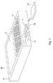
図1は、本発明の代表的な実施形態の電子デバイス100及び較正記憶デバイス150の斜視図を示す。デバイス100は、ハウジング105、ディスプレイ110、データ入力装置115、ポート120、及びセンサアレイ130を含んでもよい。上述のように、デバイス100は、任意の電子デバイス、たとえばBGMであってもよい。較正記憶デバイス150は、デバイス100内に挿入可能であってもよい。較正記憶デバイス150は、デバイス100がデータを受信し得るようにデータを保持するデバイスであってもよい。たとえば、較正記憶デバイス150は、測定片、グルコース片又はBGM用細片カートリッジであってもよい。較正記憶デバイス150は、図2、3、6a〜c及び7を参照して、以下に詳細に述べられる。
FIG. 1 shows a perspective view of an
ハウジング150は、デバイス100の構成要素のための覆いであってもよい。デバイス100の構成要素は、ハウジング105内部に少なくとも部分的に配設されてもよい。たとえば、デバイス100は、ハウジング105内部に全体的に配設されたプロセッサ(図示せず)を含んでもよい。別の例では、デバイス100は、ワイヤレス通信可能にするアンテナ(図示せず)を含んでもよい。アンテナは、ハウジング105内部に部分的に配設されると同時に、ハウジング105の外に部分的に配設されてもよい。
The
ディスプレイ110は、グラフィカルユーザインターフェイス(GUI)を備えていてもよい。ディスプレイ110は、ユーザにデバイス100によって行われた機能に関するデータを示してもよい。ディスプレイ110は、たとえば液晶ディスプレイ(LCD)であってもよい。さらに、ディスプレイ110は、入力を受信するために装備されてもよい。すなわち、ディスプレイ110は、ユーザが、ディスプレイ110の領域に接触し、続いてプロセッサに信号を送信することを可能にするタッチスクリーンであってもよい。
The
データ入力装置115は、ユーザに、データを入力するためのインターフェイスを提供してもよい。たとえば、データ入力装置115は、キーパッドであってもよい。キーパッドは、従来の方法、たとえばアルファベット順、QWERTY形式等で配列されてもよい。データ入力装置115は、ナビゲーションデバイス、たとえばタッチパッド、マウス等をさらに含んでもよい。データ入力装置115がハウジング105の単一面上に配列されていることは、単に代表例であることに留意すべきである。当業者においては、入力装置115が、ハウジング105の異なる表面上、ハウジング105の複数の面上等に配列されてもよいことが理解されよう。
ポート120は、別の構成要素がデバイス100によって受容され得るアクセス部位として機能してもよい。たとえば、ポート120を用いて、較正記憶デバイス150が受容されてもよい。較正記憶デバイス150は、方向dに動かすことによって、ポート120内に挿入されてもよい。較正記憶デバイス150は受容されると、くぼみ125に進入してもよい。ポート120又はくぼみ125は、ロッキング機構(図示せず)を装備していてもよく、これが較正記憶デバイス150と結合することにより、較正記憶デバイス150が固定して保持される。くぼみ125内にセンサアレイ130を含み、ポート120を介したアクセスを有することは、単に代表例であることに留意すべきである。デバイスの外面上のセンサアレイ等を含む他の機構、たとえば異なる形状のくぼみ及び/又はポートもまた可能である。センサアレイ130を、データポートを介してデバイス100のプロセッサに接続される外部デバイスとして含むこともまた可能であり得る。すなわち、センサアレイ130を含まないが、データポート(すなわち、プラグ又は外部デバイスからの他の接続が受容される電気コネクタ)を含む現在のデバイス100は、センサアレイ130を後付けすることができる。
センサアレイ130は、複数のセンサを含んで、較正記憶デバイス150がくぼみ125を介してポート120内に受容されたとき、データを受信してもよい。複数のセンサを用いて、較正記憶デバイス150で利用可能であるさまざまなデータを受信してもよい。しかし、複数のセンサを含むセンサアレイ130は、単に代表例であることに留意すべきである。較正記憶デバイス150は、センサによって読み取られた単一のタイプのデータを含んでもよい。このように、センサアレイ130は、較正記憶デバイス150で利用可能であるデータを受信するための1つ以上のセンサを含んでもよい。
センサアレイ130は、基板上に電磁パターンを発生させる、基板上で電気的に励起されたパッドのアレイであってもよい。電気的に励起されたの任意の周波数における電磁場は、周囲を取り巻く材料の電気特性の変化又は不均一性によって改変されてもよい。パッドのアレイにおける電界の変化を電気的に検出することによって、電気特性の画像が復元され得る。検出は、たとえば静電容量又は結合型RF界の変化を測定することによって行われてもよい。この変化は、絶縁定数又は導電率の変化に起因する場合がある。別の実施形態では、センサアレイ130は、少なくとも1つのセンサパッドが符号化パッドに結合する複数の検出パッドからのデータを解釈してもよい。以下に詳細に説明するように、結果として得られた静電容量データの読み取り値を用いてもよい。
The
静電容量又は無線周波数(RF)測定を用いて、絶縁及び/又は導電パターンを読み取ってもよい。パターンを測定したとき、画像又はデータが収集されてもよい。集積回路センサアレイを用いて、静電容量又はRF場を測定してもよい。アレイは、一次元アレイ(これによりパターンをスキャニングする)、二次元センサ(これにより領域イメージを作成する)三次元センサ(これにより立体イメージを作成する)の上を覆うパターンをスキャニングしてもよい。また、アレイは、符号化パッドと対の/対ではない検出パッドからの容量データを測定してもよい。アレイは、密度データを読み取って、250〜500ドット/インチ(dpi)の範囲の解像度を有するように設計されてもよい。このように、比較的大量のデータを、小さな領域で利用可能にし得る。 Capacitance or radio frequency (RF) measurements may be used to read the insulating and / or conductive patterns. Images or data may be collected when the pattern is measured. An integrated circuit sensor array may be used to measure the capacitance or RF field. The array may scan a pattern over a one-dimensional array (which scans a pattern), a two-dimensional sensor (which creates a region image), a three-dimensional sensor (which creates a stereoscopic image). . The array may also measure capacitive data from a detection pad that is / is not paired with a coding pad. The array may be designed to read density data and have a resolution in the range of 250-500 dots / inch (dpi). In this way, a relatively large amount of data can be made available in a small area.
静電容量測定によって、絶縁基板上の小さな導電パッドのアレイを用いて、隣接するパッド間の相互の静電容量を測定してもよい。パッド間の静電容量は、パッドのすぐ上、及びそれらの間の材料の絶縁定数によって影響される場合がある。絶縁性がより高い材料は、隣接するパッド間で測定されるより高い静電容量をもたらす場合がある。静電容量測定は、従来の測定デバイス及び関連する方法を用いてなされ得る。静電容量のマップを測定することにより、谷と隆起とのイメージを作成することができる。導電パッド及び結果として得られる静電容量測定の実施形態は、図7a〜b、8及び9を参照して、以下に詳細に説明される。 By capacitance measurement, an array of small conductive pads on an insulating substrate may be used to measure mutual capacitance between adjacent pads. The capacitance between pads may be affected by the insulation constant of the material immediately above the pads and the material between them. A more insulating material may result in a higher capacitance measured between adjacent pads. Capacitance measurements can be made using conventional measurement devices and related methods. By measuring the capacitance map, images of valleys and bumps can be created. Embodiments of the conductive pads and the resulting capacitance measurements are described in detail below with reference to FIGS. 7a-b, 8 and 9.
加えて、RF検出手法を、対象物及びその表面の電気特性に変化を検出することによって用いてもよい。放出されたRF信号は、その上に配設された材料と相互作用する場合がある。いくらかのRFエネルギは、同じ基板上の受信アンテナに反射し返される場合がある。異なる材料は、異なる反射RF信号を生じさせる場合があり、後にこれを用いて、センサアレイ上の材料のイメージを作成してもよい。また、基板上のエミッタアンテナ及び検出アンテナのアレイ上の材料は、アンテナの近接場の電磁場と相互作用すると見なされる場合がある。アレイ上の電磁特性、たとえば絶縁体誘電率又は絶縁定数の変化は、アンテナパッド間に結合された電界に影響する場合がある。結合場又は反射場強度及び/又は位相のマップを作成することにより、アレイ上の材料のマップを作成することができる。 In addition, RF detection techniques may be used by detecting changes in the electrical properties of the object and its surface. The emitted RF signal may interact with the material disposed thereon. Some RF energy may be reflected back to the receiving antenna on the same substrate. Different materials may produce different reflected RF signals that may later be used to create an image of the material on the sensor array. Also, the material on the array of emitter and detection antennas on the substrate may be considered to interact with the near field electromagnetic field of the antenna. Changes in electromagnetic properties on the array, such as dielectric constant or insulation constant, can affect the electric field coupled between the antenna pads. By creating a map of the combined or reflected field intensity and / or phase, a map of the material on the array can be created.
センサアレイ130は、容量性及び/又はRF測定に用いられてもよい。センサアレイ130は、較正記憶デバイス150上のデータをスキャニング/読み取りすることができる。較正記憶デバイス150は、容量性及び/又はRF測定を用いて符号化されてもよい。容量性及び/又はRF方法のタイプは、図6a〜c、7a〜b、8、9及び10を参照して、以下に詳細に述べられる。
The
したがって、本発明の代表的な実施形態は、較正手段として静電容量及び/又はRF信号を使用することができる。すなわち、静電容量及び/又はRF信号を用いて、予め形成された対象物のスキャニング/読み取り、静電容量のペア/非ペア状態データの判定等をおこなってもよい。容量性パターンの場合、又はセンサ(たとえばBGM)等の較正パターンを保持する基板上で使用可能である導電面がある場合、導電面は、励起電極(静電容量の場合)又は励起アンテナ(RFの場合)として較正回路に接続されてもよい。 Thus, exemplary embodiments of the present invention can use capacitance and / or RF signals as calibration means. In other words, using a capacitance and / or an RF signal, scanning / reading of a previously formed object, determination of capacitance pair / non-pair status data, and the like may be performed. In the case of a capacitive pattern, or if there is a conductive surface that can be used on a substrate that holds a calibration pattern, such as a sensor (eg, BGM), the conductive surface can be an excitation electrode (in the case of capacitance) or an excitation antenna (RF In this case) may be connected to the calibration circuit.
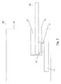
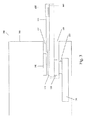
図2は、図1のデバイス100内に挿入された較正記憶デバイス150の断面図を示す。図2の断面図は、図1の斜視図に関して上述されたものに実質的に類似した構成要素を含む。たとえば、ハウジング105はセンサアレイ130を内包する。ポート120及びくぼみ125もまた図示される。加えて、断面図は、センサアレイ130の検出領域135及び細片150のパターン155をさらに示す。
FIG. 2 shows a cross-sectional view of a
センサアレイ130の検出領域135は、細片150のパターン155がスキャニング/読み取りされる位置である。センサアレイ130は、スキャニング/読み取りを実行するための回路を含んでもよい。図示されるように、検出領域135は、ハウジング105の周辺部の、くぼみ125内部に配置される。検出領域135が、たとえばガラス、ポリマー、セラミック、又はそれらの組み合わせで作られた均質又は異質のカバーを含んでもよいことに留意すべきである。異質のカバーでは、絶縁材料をパターニングして、電界の向きの線(電気力線)を検出パッド上の検出領域135に集中させることによって、データリカバリを強化することができる。たとえば、絶縁材料は、検出パッド間に配設された空隙とともにパターニングされてもよい。カバーは、検出領域135及びセンサアレイ130を保護するために与えられてもよい。くぼみ125の底側面に配置された検出領域135は、単に代表例であることに留意すべきである。当業者においては、較正記憶デバイス150のパターン155の位置に依存しており、検出領域135はくぼみ125の周辺のどこにでも配設してもよいことが理解されよう。たとえば、パターン155は、たとえば図10に示すような較正記憶デバイス150の上面に配設されてもよい。結果として、検出領域135は、くぼみ125の上部周辺に配置されてもよい。上述のように、また以下の実施形態で説明されるように、検出領域135におけるセンサアレイ130は、パターン155の符号化パッドに結合する複数の検出パッドを含んでもよい。検出アレイ130は、静電容量データを判定し、データを解釈するか又はプロセッサにデータを転送することができる。検出アレイ130がデータを解釈する場合、センサアレイ130は、たとえば集積回路(IC)、プロセッサ(たとえばマイクロプロセッサ)等を含んでもよい。
The
パターン155が較正記憶デバイス150上に配設されていることは、単なる代表例であることに留意すべきである。すなわち、パターン155は、検出アレイ130がスキャニングし得る任意の位置に配設してもよい。たとえば、パターン155は、デバイス100用のパッケージングの周辺部に配設されてもよい。別の例では、パターン155は、較正記憶デバイス150が使用前に格納されるカセットに配設されてもよい。結果として、検出アレイ130は、パターン155をスキャニングするために、ハウジング105の周辺部に向かう見通し線を含んでもよい。別の例では、パターン155は、較正記憶デバイス150用パッケージングの側面に配設されてもよい。すなわち、デバイス100の較正は、較正記憶デバイス150特有であってもよい。このように、パターン155は、較正記憶デバイス150特有であってもよい。検出アレイ130は、ハウジング105の周辺部に向かう照準線をさらに含んでもよい。さらに別の例では、パターン155は、ユーザマニュアル上又はその中に配設されてもよい。すなわち、パターン155は、ユーザマニュアルの表紙上、ユーザマニュアルのセクションのページ上等にあってもよい。複数のパターン155を含んで、異なるタイプの較正記憶デバイス150に対する異なるタイプの較正に対応させてもよい。検出アレイ130は、パターン155をスキャニングするための、ハウジング105の周辺部に向かう照準線をさらに含んでもよい。
It should be noted that the
単一のパターン155の使用は、単に代表例であることに留意すべきである。すなわち、異なるタイプの較正に複数のパターンを用いてもよい。異なるタイプの較正は、たとえば工場内規格によるデバイス100の較正、較正記憶デバイス150専用のデバイス100の較正等を含んでもよい。このように、複数のパターンは、上述の、たとえば較正記憶デバイス150、デバイス100のパッケージング、較正記憶デバイス150のパッケージング、ユーザマニュアル等の表面のいずれかに、及び任意の組み合わせで配設することができる。具体的には、パターン155は、たとえばディスペンシング記憶デバイスの場合、それぞれの較正記憶デバイス150専用であってもよい。同じパターン150が上述の種々の面に配設されてもよいことに留意すべきである。パターンを繰り返し蒸着させることは、たとえばパッケージング上に蒸着させたパターンが破損した場合のバックアップとして機能することがある。別の例では、同じパターン155は、たとえば容器が較正記憶デバイス150を内包している場合、それぞれの較正記憶デバイス150に適用してもよい。
It should be noted that the use of a
図6aは、本発明の代表的な実施形態の、第1の代表的なパターン155aの平面図を示す。パターン155aは、較正記憶デバイス150に適用することができる。すなわち、パターン155aは、較正記憶デバイス150上に配置される場合があるパターン155の一例である。パターン155aは、複数のバー601〜612を含む。たとえば、バー601、604、606、610及び612が同じ導電性及び/又は絶縁体誘電率を有してもよく、バー602、605、607及び611が同じ導電性及び/又は絶縁体誘電率を有してもよく、バー603、608及び609が同じ導電性及び/又は絶縁体誘電率を有してもよく、これによってパターンが作成される。多様なコントラストは、たとえば印刷可能な材料又はパターニングされた薄膜材料を用いて達成することができる。多様なコントラストを用いて、較正記憶デバイス150に関係した電気特性を調整することができる。たとえば、コントラストを用いて、相対的な導電性及び/又は絶縁体誘電率を変更してもよい。このように、センサアレイ130が静電容量センサである場合、パターン155aを通過する電磁界は、固有のイメージ/スキャンを生成する場合がある。結果として得られるイメージ/スキャンは、較正の目的のために用いられることができる。複数のバー601〜612が異なる暗度を呈することは、相対的な導電性及び/又は絶縁体誘電率を例証するための単なる代表例であることに留意すべきである。当業者においては、バー601〜612は多様な導電性及び/又は絶縁体誘電率を有しているが、バー601〜612の外観は同一であってもよいことが理解されよう。
FIG. 6a shows a top view of a first
図6bは、本発明の代表的な実施形態の、第2の代表的なパターン155bの平面図を示す。パターン155bは、較正記憶デバイス150に適用することができる。すなわち、パターン155bは、較正記憶デバイス150上に配置される場合があるパターン155の別の例である。パターン155bは、複数のバー625〜633を含む。バー625〜633は、多様な幅を含む。この代表的な実施形態では、物理的特性(すなわち幅)が用いられる。たとえば、バー625〜629及び633は中程度の幅を有する。バー630及び632は広い幅を有する。バー631は狭い幅を有する。多様な幅は、たとえばインク又は任意の他の印刷可能な材料、ポリマーから形成された三次元構造、エッチングされた金属又は半導体等を用いることによって達成することができる。センサアレイ130が静電容量センサである場合、パターン155bを通過する電磁界は、固有のイメージ/スキャンを生成する場合がある。結果として得られるイメージ/スキャンは、較正の目的のために用いられることができる。多様な幅は、センサアレイ130がRFセンサである場合にも用いられてもよい。すなわち、生成されたRF信号は、反射されたとき、多様な変動を有する場合がある。たとえば、より幅広いバー630及び632は広幅に反射し、一方で幅の狭いバー631は、希薄に反射する。パターン155bの特性(すなわち幅)は、図6aのパターン155aに組み込まれてもよいことに留意すべきである。さらに、パターン155aの特性(すなわちコントラスト)は、パターン155bに組み込まれてもよいことにも留意すべきである。
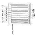
FIG. 6b shows a plan view of a second
図6cは、図6bの第2の代表的なパターン155bの側面図を示す。図6cは、複数のバー625〜633を再度示す。この代表的な実施形態では、バー625〜633は、多様な幅及び多様な長さを含む。図6bを参照して上述されたように、バー625〜633の幅は、上記説明と合致する。しかし、幅は、上記説明と異なってもよい、すべてが同じでもよい等であることに留意すべきである。バー625、627、630及び633は中間的な幅を有する。バー628は、高い高さを有し、バー632は、最も高い高さを有する。バー626、629及び631は、低い高さを有する。多様な高さは、たとえばインク又は任意の他の印刷可能な材料、ポリマーから形成された三次元構造、エッチングされた金属又は半導体等を用いることによって達成することができる。センサアレイ130が静電容量センサである場合、パターン155bを通過する電磁界は、固有のイメージ/スキャンを生成する場合がある。結果として得られるイメージ/スキャンは、較正の目的のために用いられることができる。多様な高さは、センサアレイ130がRFセンサである場合にも用いられてもよい。すなわち、生成されたRF信号は、反射されたとき、多様な変動を有する場合がある。たとえば、近接場測定では、多様な高さは、反射時の多様な信号強度をもたらす。パターン155bの特性(すなわち高さ)は、図6aのパターン155aに組み込まれてもよいことに留意すべきである。さらに、パターン155aの特性(すなわちコントラスト)は、パターン155bに組み込まれてもよいことにも留意すべきである。
FIG. 6c shows a side view of the second
パターン155bの物理的特性(すなわち高さ、幅、又はそれらの組み合わせ)が、さまざまな方法を用いて作成されてもよいことに留意すべきである。たとえば、高さ及び/又は幅は、予め成型、パンチング、スタンピング、エッチング、レーザスクライブ等されてもよい。特に、電気化学センサでは、すでに存在する導電パターンは、たとえばレーザアブレーションによって改変されて、パターンを作成してもよい。パターンは、センサの電気的検出特性を著しく変えるのではなく、それでも読み取り可能な較正パターンを作成するような方法で形成されてもよい。さらに、パターン155bの高さ及び/又は幅は反転されてもよい。すなわち、多様な高さ及び/又は幅が較正記憶デバイス150に作成されてもよく、較正記憶デバイス150の表面の一部の延長部として作成されることとは対照的である。加えて、多様な高さ/幅は、延長部及びキャビティの組み合わせであってもよい。
It should be noted that the physical characteristics of
当業者においては、パターン155a〜bは単に代表例であることが理解されよう。パターン155a〜bは、上面から見たとき、実質的にバーコードに類似する。このように、パターン155a〜bは、バーコードの特徴も呈する。たとえば、バーコードは、一次元的、二次元的、三次元的等に符号化されてもよい。パターン155a〜bは、実質的に一次元バーコードに類似している。しかし、パターン155a〜bはまた、実質的に二次元バーコード又は三次元バーコードに類似していてもよい。すなわち、たとえば、センサアレイ130がパターンをスキャニング/読み取りして、較正記憶デバイス150上に二次元パターンに対応するイメージを生成してもよい。さらに、パターン155は、一次元、二次元、及び/又は三次元バーコードのいずれをも実質的に示してもよい。
Those skilled in the art will appreciate that
加えて、バーコードの使用、特に二次元バーコードに関しては単に代表例である。すなわち、二次元バーコードは、任意の二次元較正パターンを表してもよい。このように、二次元較正パターンは、パターン155a〜bとして用いられてもよい。たとえば、二次元較正パターンは、一次元センサアレイの軸を基準として、及びそれに垂直にスライドさせて、二次元較正パターンが読み取られるようにしてもよい。三次元バーコードについても同じことが適用されてもよい。
In addition, the use of barcodes, especially two-dimensional barcodes, is merely representative. That is, the two-dimensional barcode may represent an arbitrary two-dimensional calibration pattern. Thus, the two-dimensional calibration pattern may be used as the
図6a〜cを参照して示された上記の例は、センサアレイ130が、内部に包含されたデータをスキャニング/読み取りするタイプのパターン155を示す。すなわち、センサアレイ130は、静電容量及び/又はRFデータを包含する任意のタイプのパターンを読み取るのが一般的である。別の実施形態では、上述のように、センサアレイ130は、複数の検出パッドを含んでもよく、検出パッドの少なくとも1つが、パターン155の符号化パッドに結合する。すなわち、センサアレイ130は、対応するタイプのパターンの読み取り専用であってもよい。さらに、検出パッドを符号化パッド又は非結合検出パッドと結合することにより、較正の目的のために用いられる静電容量データをもたらすことができる。
The above example shown with reference to FIGS. 6a-c shows a
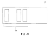
図7aは、本発明の代表的な実施形態の、センサアレイ130の検出パッド805の平面図を示す。この代表的な実施形態では、センサアレイ130は、4つの検出パッド805を含む。検出パッド805は、プリント回路基板(PCB)815上に配設されてもよい。代表的な実施形態では、センサアレイ130は、最大数の検出パッド805を含む。図7bは、本発明の代表的な実施形態の、図7aの検出パッド805と結合された符号化パッド820を含む、第3の代表的なパターン155の平面図を示す。上述のように、センサアレイ130は、最大数の検出パッド820を含んでもよい。したがって、パターン155は、検出パッド805の最大数まで符号化パッドを含んでもよい。代表的な実施形態では、第3のパターン155は、3つの符合化パッド820(すなわち、4つよりも少ない最大数)を含むことができる。図示されるように、符号化パッド820は、第1、第3及び第4の位置に配設され、第1の位置は最も左である。検出パッド805は、たとえば導電トランスであってもよく、一方で符号化パッド802は、たとえば金属薄膜パッドであってもよい。検出パッド805は、それ自体がコンデンサの一部であってもよく、又は金属パッドに結合された場合、より大きなコンデンサとなってもよい。
FIG. 7a shows a plan view of the
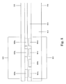
図8は、本発明の実施形態の、図7aの検出パッド805の、図7bの符号化パッド820との結合を示す。上述のように、センサアレイ130の検出パッド805は、PCB815上に配設されてもよい。図8は、検出パッドが絶縁層810で覆われてもよいことをさらに図示する。絶縁層810は、静電容量測定に加えて、符号化パッド820との結合に使用されてもよい。パターン155が正しい方向であるとき、符号化パッド820は、対応する検出パッド805と整合することに留意すべきである。
FIG. 8 illustrates the coupling of the
上述のように、符号化パッド820の検出パッド805との結合は、静電容量データを提供する場合がある。代表的な実施形態では、符号化パッド820は、820x〜zを含んでもよく、一方で検出パッド805は検出パッド805a〜dを含む。たとえば、電流は検出パッド805に供給されてもよく、静電容量データが読み取られてもよい。図示されるように、検出パッド805a、c及びdは、符号化パッド820x、y及びzにそれぞれ結合され、これに対して、検出パッド820bは非結合である。検出パッド805が
符号化パッド820に結合される場合、符号化パッド820の組成(たとえば、金属薄膜)に起因して、より大きなコンデンサが作成される。検出パッド805の結合/非結合を用いて、バイナリコードを作成してもよい。すなわち、結合されたパッドは、符合1(C1)を表してもよく、一方で非結合パッドは、符合0(C0)を表してもよい。このように、図8の代表的な実施形態は、C1C0C1C1のバイナリコードを有していてもよい。このバイナリコードは、パターン155専用であってもよい。したがって、各タイプの較正記憶デバイス150が、対応するバイナリコードを表すそれぞれのパターン155を含んでもよい。代表的な実施形態のセンサアレイが4つの検出パッド805を含むため、バイナリコード文字列の総数は、16(24)である。センサアレイ130が任意の数の検出パッドを含んでもよいことに留意すべきである。さらなる検出パッドが、さらなるタイプのバイナリコードに対応してもよい。たとえば、5つの検出パッドは32文字列(25)になり、6つの検出パッドは64文字列(26)になり、10個の検出パッドは1024文字列(210)になる等である。
As described above, the coupling of
図9は、本発明の代表的な実施形態の、図8の対状に実質的に類似した別の対状の概略図である。図9は本発明の代表的な実施形態であり、3つの符号化パッド920を含むパターン155が接地されている。センサアレイ130は、PCB910上に配設された7つの検出パッド905を含み得る。検出パッド905は、PCB910がすでに電子デバイス100内に存在する場合、PCB910上に直接形成されてもよい。また、PCB910上には、静電容量・ディジタル変換器集積回路(CDC−IC)915が配設されている。CDC−IC915は、検出パッド905から静電容量測定値を受信し、測定値をディジタル形式に変換して、たとえばマイクロプロセッサ145に転送してもよい。マイクロプロセッサ145もまた、PCB910上に配設されてもよいことに留意すべきである。さらに、上述のように、マイクロプロセッサ145は、センサアレイ130の一部、電子デバイスのプロセッサ等であってもよい。
FIG. 9 is another pair of schematics substantially similar to the pair of FIG. 8 of an exemplary embodiment of the present invention. FIG. 9 is an exemplary embodiment of the present invention, where a
CDC−IC915は、たとえば、Analog Devices, Inc.製造の型番AD7142であってもよい。上述のように、CDC−IC915は、7つの検出パッド905に接続されてもよい。このように、場合によっては最大128文字列のバイナリコードがあってもよい。したがって、CDC−IC915は、解像度128ビットを有していてもよい。代表的な実施形態では、CDC−IC915を装備して、1x10⁻¹⁵Fの静電容量変化の相違を検出してもよい。さらに、CDC−IC915を装備して、検出回路に対する環境変化、たとえば温度、湿度等の変化を自動的に較正してもよい。また、CDC−IC915は、シールド925に接続していてもよい。シールド925は、干渉、たとえば電磁干渉(EMI)、RF干渉等から、センサアレイ130及びパタ−ン155の構成要素を隔離することを支援してもよい。
CDC-IC915 is available from, for example, Analog Devices, Inc. The model number AD7142 of manufacture may be sufficient. As described above, the CDC-
本発明の代表的な実施形態では、CDC−IC915は、検出パッド905からの静電容量測定値をさまざまな方法で解釈し得る。当業者においては、外的要因(たとえば、EMI、環境等)に起因して、安定した静電容量測定値は確認されなくてもよいことが理解されよう。代表的な実施形態がバイナリコードを使用するため、静電容量測定値は、C0(非結合センサパッドを表す)又はC1(符号化パッドを有する結合センサパッドを表す)であり得る。このように、値C0及びC1に必ずしも一致しない測定値を補償するために、CDC−IC915は、あらゆる入力測定値を分類してもよい。
In an exemplary embodiment of the invention, the CDC-
CDC−IC915は、偏りを評価することで、入力測定値を分類してもよい。たとえば、値C0及びC1は、制御手順によって判定することができる。制御手順は、C0が最小静電容量測定値に対応し、一方でC1が最大静電容量測定値に対応することを判定することができる。当業者においては、静電容量測定値は、部分的に温度及び湿度の関数であることが理解されよう。このように、検出パッドに近接するユーザを含む周辺の移動性の金属は、静電容量測定値に影響する場合がある。上述のように、CDC−IC915は、干渉を較正し、シールド925を使用する等することができる。また、CDC−IC915は、静電容量測定値への影響を、防害静電容量環境値ドリフトにより分類し得る。いったん分類されると、CDC−IC915は、干渉を補償して、正しい静電容量測定値を算出する。
The CDC-
加えて、干渉がなくても、静電容量測定値は、依然として必ずしも値C0及びC1と対応しないかもしれない。偏りを評価することに戻り、C0とC1との間の中間値は、必ずしもC0及びC1ではない入力静電容量測定値の分類のベースとして用いられてもよい。中間値は、たとえば、値C1から値C0を減じて2で除したもの(Cm=(C1−C0)/2)であり得る。値C1が値C0よりも大きいのは、符号化パッドに結合されたセンサパッドがより大きなコンデンサを作成するためであることに留意すべきである。入力静電容量測定値は、値Cmと比較される場合がある。測定値がCmより小さい場合、測定値はその後、C0と指定される場合がある。測定値がCmより大きいか又は等しい場合、測定値はその後、C1と指定される場合がある。このように、CDC−IC915は、それぞれの検出パッド905からの静電容量測定値を解釈して、パターン155に関連する対応するバイナリコードを判定することができる。図9の代表的な実施形態では、CDC−IC915は、パターン155がC1C0C1C0C0C0C1のバイナリコードを含むことを判定し得る。ディジタル化されたコードは、マイクロプロセッサ145に転送されてもよく、ここでコードを解釈して、電子デバイスのための正しい較正を実行してもよい。
In addition, even without interference, the capacitance measurement may not necessarily correspond to the values C0 and C1. Returning to assessing bias, the intermediate value between C0 and C1 may be used as the basis for classification of input capacitance measurements that are not necessarily C0 and C1. The intermediate value can be, for example, the value C1 minus the value C0 divided by 2 (Cm = (C1-C0) / 2). It should be noted that the value C1 is greater than the value C0 because the sensor pad coupled to the encoding pad creates a larger capacitor. The input capacitance measurement may be compared with the value Cm. If the measured value is less than Cm, the measured value may then be designated as C0. If the measured value is greater than or equal to Cm, the measured value may then be designated as C1. In this way, the CDC-
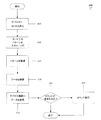
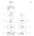
図4は、本発明の代表的な実施形態の、較正の方法400を示す。方法400は、図1〜2のデバイス100及び較正記憶デバイス150を参照して説明される。また、方法400は、図6a〜cの種々のパターン155a〜bを参照して説明される。方法400は、較正記憶デバイス150上のパターン155を使用して、機能実行に備えてデバイス100を較正する。以下に詳細に説明されるように、方法400を用いて、デバイス100を自動的に較正してもよい。すなわち、デバイス100の較正は、別個のステップ又は調整を必要とすることなく行うことができる。具体的には、較正は、機能を実行する前に別個に操作される、デバイス100の回路、プロセッサ、メモリ等を必要としない。
FIG. 4 illustrates a
ステップ405では、較正記憶デバイス150は、方向dに動かすことにより、ポート120を介してデバイス100内に挿入される。較正記憶デバイス150は、くぼみ125内に保持されてもよい。本発明の代表的な実施形態により、較正記憶デバイス150が正しい方向で挿入されると、較正記憶デバイス150の構成要素は、デバイス100の対応する構成要素に整合することができる。たとえば、パターン155は、検出領域135上に位置付けられてもよく、それによりセンサアレイ130はパターン155をスキャニング/読み取りし得る。
In
較正記憶デバイス150がデバイス100内に挿入されることは、単に代表例であることに留意すべきである。たとえば、較正記憶デバイス150は、デバイス100から離れた距離で空中停止しているか又は配置されてもよい。検出領域135は、くぼみの部分ではないハウジング105の一部上であってもよい。このように、較正記憶デバイス150が空中停止しているか又は配置されている領域は、ハウジング105上に部分的に配設された検出領域135上であってもよい。
It should be noted that the
ステップ410では、較正記憶デバイス150のパターン155は、センサアレイ130によって読み取り/スキャニングされる。上述のように、パターン155は、較正記憶デバイス150の底側面に配設されてもよい。結果として、センサアレイ135は、くぼみ125内部の対応する領域に配設されてもよい。センサアレイ130は、たとえば静電容量測定値及び/又はRF測定値を用いてパターン155を読み取り/スキャニングしてもよい。パターン155は、図6a〜cのパターン155a〜bを参照して上記で説明されたような一次元又は二次元的特徴(たとえば、コントラスト、幅、高さ等)を含んでもよい。また、パターン155は、図7a〜b、8及び9を参照して上記で説明されたようなペア/非ペア状態の検出パッド及び符号化パッドを用いて読み取られてもよい。
In
ステップ415では、パターン155が解読される。パターン155は、機能の実行に備えてデバイスを設定するパラメータデータを含んでもよい。たとえば、パターン155bのバー625〜633の多様な高さは、このデータを含んでもよい。センサアレイ130は、デバイス100のプロセッサに、読み取られた/スキャニングされたパターン155を送信してもよい。プロセッサは、センサアレイ130によって送信された生データからパターン155を解読してもよく、又はセンサアレイ130はパターン155を解読して、解読されたデータをプロセッサに送信するために装備されてもよいことに留意すべきである。
In
ステップ420では、データが解釈される。上述のように、パターン155は、パラメータデータを含んでもよい。パターン155のデータが解釈されて、パラメータデータが含まれていることを示す場合がある。データは、プロセッサによって、又はセンサアレイ130によって解釈されてもよいことに留意すべきである。このように、プロセッサは、パターン155に関する生データ又は解読されたデータを受信して、そこから解釈することができる。加えて、センサアレイ130は、パターン155の解読されたデータを解釈して、プロセッサに解釈されたデータを送信するために装備されてもよい。
In
ステップ425では、データは、デバイス100の機能性のために使用される。パターン15のデータがパラメータデータを含む場合、デバイス100はこのデータを使用して、種々のパラメータを設定することができる。たとえば、較正記憶デバイス150は、パターン155が提供する以上の他の用途、たとえばさらなるデータ送信のために用いられてもよい。このさらなるデータは、デバイス100がどのように構成されているかに依存する場合がある。まず、パターン155に含まれたパラメータデータに従ってデバイス100を設定することによって、デバイス100が正しく構成されて(たとえば較正されて)、さらなるデータを受信することができる。別の例では、パターン155は、ドライバデータを含んでもよい。ドライバデータを用いて、デバイス100を、別に電子デバイスであるかもしれない較正記憶デバイス150のデータを理解して受信するように構成することができる。較正記憶デバイス150のデータは、種々の異なる機能性に関連する複数のデータ形式を含んでもよいことに留意すべきである。
In
ステップ430では、パターン155がコマンドデータを含むかについての判断がなされる。すなわち、パターン155は、デバイス100によって実施される動作を示すデータをさらに含んでもよい。コマンドデータは、たとえば、デバイス100にインストールされたプログラムの開始を含んでもよい。パターン155に含まれるコマンドを実行することによって、デバイス100は、較正記憶デバイス150に関連する機能を実行するための準備をすることができる。ステップ430が、コマンドデータが含まれていないと判断した場合、方法400は終了する。しかし、ステップ430が、コマンドデータが含まれていると判断した場合、ステップ435で対応する動作が取られて、コマンドデータを実行する。機能性に使用されたデータに類似して、種々の機能性を含む複数のコマンドもまた含まれてもよいことに留意すべきである。
In
方法400のステップは単に代表例であることに留意すべきである。さらなるステップをふくんで、方法400を拡張してもよい。たとえば、パターン155は、比較的大量のデータを含む、高密度の二次元のものであってもよい。パターン155は、解読されて(すなわちステップ415)解釈され(すなわちステップ420)、初期データが使用されている(すなわちステップ425)ことを示してもよい。その後、コマンドが実行されてもよい(すなわちステップ430)。さらに、パターン155は、コマンドを実行するとき、後続データが使用されることを示すデータを含んでもよい。したがって、パターン155に含まれるデータ量及びデータ型に依存して、方法400にさらなるステップが含まれてもよい。
It should be noted that the steps of
図3は、本発明の代表的な実施形態の、血糖計(BGM)300の断面図を示す。すなわち、図3は、図1〜2のデバイス100及び較正記憶デバイス150を適用することができる特定の例を図示する。しかし、上述のように、BGMは単に代表例であり、デバイス100及び較正記憶デバイス150は、以下に説明されるように、さまざまな他の用途及び検体(上記では「分析対象物」と呼ばれる)に適用してもよい。加えて、上述のように、BGM300は、分析対象物計を表してもよい。BGM300は、図1〜2のデバイス100に実質的に類似した構成要素を含む。たとえば、BGM300は、ハウジング105、ポート120、くぼみ125、センサアレイ130及び検出領域135を含む。BGM300は、コネクタ140をさらに含む。コネクタ140は、別個のデバイスからデータを受信するための電線管であってもよい。コネクタ140は、血液試料に関するデータを受信し得る。
FIG. 3 shows a cross-sectional view of a blood glucose meter (BGM) 300 according to an exemplary embodiment of the present invention. That is, FIG. 3 illustrates a specific example in which the
図3は、本発明の代表的な実施形態の較正記憶デバイス350をさらに示す。較正記憶デバイス350は、BGM300用のグルコース片又は細片カートリッジであってもよい。一般的に、較正記憶デバイス350は、分析対象物を受ける細片であってもよい。較正記憶デバイス350は、図1〜2の較正記憶デバイス150に実質的に類似した構成要素を含む。たとえば、較正記憶デバイス350は、パターン155を含む。パターン155は、特定の較正及び試験パラメータに関するデータ、製造データ、別個の全血及び血漿較正、偽造防止コード等を含んでもよい。較正記憶デバイス350は、反応チャンバ160、電極170及び蓋175をさらに含む。反応チャンバ160は、血液試料が配置される付着領域である場合がある。反応チャンバ160は、血液試料を分析する種々の化学物質、デバイス等を含んでもよい。血液試料の分析から結果として得られるデータは、電極170を介して、較正記憶デバイス350の長さ方向に沿って送信されてもよい。電極170の露出領域は、コネクタ140と結合して、BGM300が血液試料データを受信することが可能になるようにしてもよい。蓋175は、電極170を破損させる外力を遮断する、任意の保護層であってもよい。蓋175は、たとえばガラス、ポリマー等であってもよい。
FIG. 3 further illustrates a
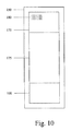
図10は、本発明の代表的な実施形態の、第4の代表的なパターン180の図を示す。図6a〜cを参照して上述されたように、パターン155は、較正記憶デバイス150の底側面に配設されてもよい。図3に図示されるように、パターン155はまた、較正記憶デバイス350の底側面に配置される。すなわち、パターン155は、電極170と異なる側面にある。しかし、上述のように、また図10に示されるように、パターン155は、種々の他の位置に配置されてもよい。図10は、上述のように、較正記憶デバイス350の構成要素を含む。また、図10は、電極170の同面上に配置されたパターン180を示す。図示されるように、パターン180は露出された電極180の一部上にエッチングされてもよい。結果として、検出領域135は、動作可能位置にあるときにパターン180の予想される配置に対応する、くぼみ125の上面上に配置されてもよい。パターン180は、いずれかの特徴(たとえば、コントラスト、高さ、幅、又はそれらの組み合わせ)を含んでもよく、また図6a〜cを参照して上記で説明された方法のいずれかを用いて作成されてもよい。電極170上のパターン180の位置は、単に代表例であることに留意すべきである。パターン180は、蓋175上に配置されてもよい。結果として、検出領域135はやはり、くぼみ125内部の対応する位置にある。たとえば、検出領域135は、コネクタ140に関連するポート120に近接した位置にあってもよい。パターン180は、特定の較正及び試験パラメータに関するデータ、製造データ、全血及び血漿の個別の較正、偽造防止コード等を含んでもよい。
FIG. 10 shows a diagram of a fourth
図5は、図3のBGM300のための較正方法500を示す。方法500は、図3のBGM300及び較正記憶デバイス350を参照して説明される。また、方法500は、図6a〜cの種々のパターン155a〜b及び図10のパターン180を参照して説明される。方法500は、較正記憶デバイス350上のパターン155又は180を使用して、血液試料の分析に備えてBGM300を較正する。すなわち、BGM300は、用いられる較正記憶デバイス350のタイプにより、血液試料の受容に備えてパラメータを設定する。較正記憶デバイス350は、図3を参照して上記で説明された試験片であってもよい。
FIG. 5 shows a
ステップ505では、較正記憶デバイス350は、方向dに動かすことにより、ポート120を介してBGM300内に挿入される。較正記憶デバイス350は、くぼみ125内に保持されてもよい。代表的な実施形態では、較正記憶デバイス350は、電極端及び反応チャンバ端を含む。電極端は、露出された電極170を含む。反応チャンバ端は、反応チャンバ160を含む。反応チャンバ160が血液試料を受容するように設計されているため、較正記憶デバイス350の反応チャンバ端は、デバイス300から延伸されている。続いて、較正記憶デバイス350の電極端が、ポート120を介してくぼみ125内に挿入される。較正記憶デバイス350がデバイス300内に挿入されることは、単に代表例であることに留意すべきである。較正記憶デバイス350は、方法400で効果的に上述したように、空中停止しているか又は配置されてもよい。
In
ステップ510では、較正記憶デバイス150のパターン155又は180は、センサアレイ130によって読み取り/スキャニングされる。パターン155は、方法400のステップ410に関連して上記で説明されたものと実質的に類似した方法で読み取り/スキャニングされてもよい。また、図10のパターン180も、実質的に類似した方法で読み取られてもよい。しかし、上述のように、検出領域135は、較正記憶デバイス350上のパターン180の位置により、対応する位置に配置される。パターン180は、較正記憶デバイス350の上面上に配設され、結果として、検出領域135はくぼみ125の上面上に配置される。
At
ステップ515では、パターン155又は180が解読される。ステップ520では、データが解釈される。ステップ515の解読及びステップ520の解釈は、それぞれステップ415の解読及びステップ420の解釈について上記で説明されたものと実質的に同じ方法で行われてもよい。上述のように、パターン155又は180は、特定の較正及び試験パラメータに関するデータ、製造データ、別個の全血及び血漿較正、偽造防止コード等を含んでもよい。
In
ステップ525では、BGM300は、パターン155又は180に含まれるデータに従って較正される。方法400のステップ425は、デバイス100の機能性のためのデータを使用することを説明した。ステップ525は、BGM300のための、パターン155又は180上のデータを使用する1つの代表的な実施形態を説明する。すなわち、較正記憶デバイス350に含まれるデータは、パラメータデータを含んでもよい。パラメータデータは、BGM300が、受信される血液試料のデータを正しく解釈、受信等をするために準備すべき種々の設定を表示してもよい。すなわち、BGM300は、較正記憶デバイス350がパターン155又は180を含むのであれば、任意のタイプの較正記憶デバイス350を受容してもよい。較正記憶デバイス350は、血液試料データを、さまざまな方法で送信することができる。このようにBGM300を所定の方法で較正することにより、BGMが血液試料を分析することを可能にすることができる。較正データが、単一の血液試料で行われる複数の診断試験用であってもよいことに留意すべきである。たとえば、較正記憶デバイス350が種々の診断試験に用いられる場合、較正データは、BGMがさまざまな診断試験を行う準備に用いられてもよい。
In
ステップ530では、較正記憶デバイス350の反応チャンバ160上に血液試料が配置される。上述のように、反応チャンバ160は、付着させた血液試料と反応するさまざまな化学物質を含む。反応すると、血液試料に関するデータが収集される。たとえば、1つの化学物質は、血液試料中のグルコースレベルを判定し得る。結果として得られる測定値は、電極170を通して送信されてもよい。データは、電極170を通してさまざまな方法で送信されてもよいことに留意すべきである。たとえば、較正記憶デバイス350は、電源及び回路を含んで、データを電気的に転送してもよい。別の例では、電極は、反応チャンバ160とともに機能する化学インジケータを含んでもよい。化学インジケータは、血液試料に関する種々の基準を判定するためのゲージとして用いられてもよい。
In
ステップ535では、血液試料が測定される。血液試料の測定は、反応チャンバ160、電極170、又はそれらの組み合わせからのデータを判定したときに行われ得る。コネクタ140は、較正記憶デバイス350をデバイス300と結合させて、較正記憶デバイス350からデバイス300へのデータ送信を可能にするように機能してもよい。血液試料の測定は、較正記憶デバイス350の構成要素、デバイス300のプロセッサ、デバイス300の測定要素(図示せず)等によって行われてもよいことに留意すべきである。ステップ540では、血液試料の分析結果が表示される。たとえば、結果は、血糖濃度、血液型、赤血球数等を含んでもよい。たとえばディスプレイ110を用いて、結果を表示してもよい。
In
方法500のステップは、単に代表例であることに留意すべきである。方法500は、さらなるステップを含んでもよい。たとえば、方法400に類似して、較正記憶デバイス350は、BGM300を実行させるためのコマンドを含んでもよい。パターン155又は180は、BG300を実行させて、血液試料の入力データを正しく分析するためのコマンドを含んでもよい。コマンドは、たとえば1つのタイプの較正記憶デバイス350上に配置された血液試料を分析するために必要とされるプログラムの実行に関連する場合がある。別の例では、BGM300を最初に、検出領域135のみを稼働させながら、非活性化させてもよい。検出領域135がパターン155又は180を検出した時、BGM300を稼働させて、方法500を続行してもよい。
It should be noted that the steps of
BGM300に関連して説明された本発明は、単に代表例であることに再度留意すべきである。本発明は、さまざまな用途に用いることができる。たとえば、較正記憶デバイス350は、識別用較正記憶デバイスであってもよい。パターン155は、ユーザ個々の、デバイス100の固有の一次元又は二次元シーケンスであってもよい。すなわち、較正記憶デバイス150がデバイス100内に挿入されると、検出アレイ130は、パターン155を読み取り/スキャニングして、認証されたユーザがデバイス100を稼働させているかを判断してもよい。別の例では、較正記憶デバイス150は、導入用較正記憶デバイスであってもよい。パターン155は、デバイス100が従う命令セットを含んでもよい。命令に従うと、デバイス100は、パターン155に含まれたデータに対応するさらなる機能を行うことが可能になる場合がある。さらに別の例では、較正記憶デバイス150は復号コードを含んでもよい。較正記憶デバイス150のデータ、コマンド、命令等は、暗号化されてもよい。このように、デバイス100がパターン155を読み取り/スキャニングすると、デバイス100は、復号化方法を学習して、較正記憶デバイス150のデータを読み取る。
It should be noted again that the present invention described in connection with
パターン155又は180が暗号化されてもよいことにもまた留意すべきである。したがって、パターン155又は180を復号化するための装備を有するデバイスのみが、較正記憶デバイス150に関する機能を使用することができる。
It should also be noted that the
本発明の代表的な実施形態は、電子デバイスを較正するための簡易かつ低コストな電気的読み取り技術を可能にする。本発明の代表的な実施形態の1つの代表的な利点は、電子デバイスを較正するために多くの場合必要とされる、物理的な導電電気接点を取り除くことである。たとえば、正しい較正を行うためには、電子デバイスを電気的に接続するための別個のコンピューティングデバイスが必要とされる場合がある。さらに、この電気接続は、電子デバイスに不必要な湿潤性の分解をもたらすかもしれない。本発明の代表的な実施形態の別の代表的な利点は、現在用いられている較正方法と比較して、較正用ラベルの生産コストが低いことである。本発明の代表的な実施形態は、電子デバイスを正しく較正するために、センサアレイ及びラベルのみを必要とする。種々の電子デバイスが、すでにセンサアレイに装備されていてもよい。したがって、ラベルの製造が、要求されるのみである。ラベル自体は安価に作られてもよく、その中で符号化されるために必要とされるデータ量に依存する。本発明の代表的な実施形態さらなる別の代表的な利点は、ラベル及びその中で符号化されるデータは、任意の既存の製造技術又は電子デバイスに後付けされてもよいことである。たとえば、ラベルは、別に製造されてもよく、また較正記憶デバイスに添付されてもよい(たとえば、グルコース片、細片カートリッジ等)。また、電子デバイスは、外部センサアレイに接続されてラベルをスキャニングし、これにより電子デバイスを較正してもよい。 Exemplary embodiments of the present invention allow a simple and low cost electrical reading technique for calibrating electronic devices. One exemplary advantage of an exemplary embodiment of the present invention is to eliminate physical conductive electrical contacts that are often required to calibrate an electronic device. For example, a separate computing device for electrically connecting the electronic device may be required to perform a correct calibration. Furthermore, this electrical connection may result in unnecessary wettable degradation for the electronic device. Another exemplary advantage of exemplary embodiments of the present invention is that the production cost of the calibration label is low compared to currently used calibration methods. Exemplary embodiments of the present invention require only a sensor array and label to correctly calibrate the electronic device. Various electronic devices may already be installed in the sensor array. Therefore, only label production is required. The label itself may be made inexpensively and depends on the amount of data required to be encoded therein. Exemplary Embodiments of the Invention Yet another exemplary advantage is that the label and the data encoded therein may be retrofitted to any existing manufacturing technology or electronic device. For example, the label may be manufactured separately and attached to a calibration storage device (eg, glucose strip, strip cartridge, etc.). The electronic device may also be connected to an external sensor array to scan the label, thereby calibrating the electronic device.
当業者においては、本発明の本質及び範囲から逸脱することなく、本発明に種々の改変がなされてもよいことが明白であろう。したがって、本発明は、添付の特許請求の範囲およびそれらの等価物の範囲内から提供されるような本発明の改変および変形を網羅していることが意図される。 It will be apparent to those skilled in the art that various modifications can be made to the present invention without departing from the spirit and scope of the invention. Thus, it is intended that the present invention cover modifications and variations of this invention as provided within the scope of the appended claims and their equivalents.
Claims (33)
センサアレイからデータを受信して、データに従ってデバイスを較正するプロセッサと、
を含むデバイス。 A sensor array that collects data from a pattern contained in a calibration storage device based on one of a capacitance measurement and a radio frequency measurement;
A processor that receives data from the sensor array and calibrates the device according to the data;
Including device.
パターンに含まれるデータを判定することと、
データに従ってデバイスを較正することであって、その較正が、較正記憶デバイスとともに機能を行うようにデバイスを準備することを含むことと、
を含む方法。 Reading a pattern contained on the calibration storage device using at least one of a capacitance measurement and a radio frequency measurement;
Determining the data contained in the pattern;
Calibrating the device according to the data, the calibration including preparing the device to perform a function with a calibration storage device;
Including methods.
静電容量測定及び無線周波数測定のうち少なくとも1つを用いて、分析対象物受容片上に配設されたパターンを読み取ることと、
パターン内に含まれた較正データを判定することと、
較正データに従って、分析対象物計を較正することと、
分析対象物片上に分析対象物を受容することと、
較正された分析対象物計を用いて、分析対象物を分析することと、
分析結果を表示することと、
を含む方法。 Receiving an analyte-receiving piece by means of an analyte meter;
Reading a pattern disposed on the analyte receiving piece using at least one of capacitance measurement and radio frequency measurement;
Determining calibration data contained in the pattern;
Calibrating the analyte meter according to the calibration data;
Receiving the analyte on the analyte piece;
Analyzing the analyte using a calibrated analyte meter;
Displaying the analysis results,
Including methods.
静電容量測定及び無線周波数測定のうち少なくとも1つを用いて、パターンからデータを収集するセンサアレイと、
パターンから収集されたデータに基づいて、較正された上で分析対象物の分析を行う分析対象物計を較正するプロセッサと、
を含む分析対象物計。 A port for receiving an analyte receiving piece comprising a pattern and a reaction chamber configured to receive the analyte;
A sensor array that collects data from the pattern using at least one of capacitance measurement and radio frequency measurement;
A processor for calibrating an analyte meter that is calibrated and analyzes the analyte based on data collected from the pattern;
Analyte total including.
分析対象物を受容するように構成された反応チャンバであって、分析対象物受容片が分析対象物計によって受容されて、分析対象物計が較正されると分析対象物が分析される反応チャンバと、
を含む、分析対象物受容片。 For an analyte meter that is calibrated based on calibration data, a pattern comprising calibration data from which the pattern is read using one of a capacitance measurement and a radio frequency measurement;
A reaction chamber configured to receive an analyte, wherein the analyte receiving piece is received by the analyte meter and the analyte is analyzed when the analyte meter is calibrated When,
An analyte-receiving strip comprising:
Applications Claiming Priority (3)
| Application Number | Priority Date | Filing Date | Title |
|---|---|---|---|
| US95425507P | 2007-08-06 | 2007-08-06 | |
| US12/129,044 US7981678B2 (en) | 2007-08-06 | 2008-05-29 | System and method for automatic calibration |
| PCT/US2008/065113 WO2009020690A1 (en) | 2007-08-06 | 2008-05-29 | System and method for automatic calibration |
Publications (2)
| Publication Number | Publication Date |
|---|---|
| JP2010536035A true JP2010536035A (en) | 2010-11-25 |
| JP2010536035A5 JP2010536035A5 (en) | 2011-07-07 |
Family
ID=39743312
Family Applications (1)
| Application Number | Title | Priority Date | Filing Date |
|---|---|---|---|
| JP2010520011A Withdrawn JP2010536035A (en) | 2007-08-06 | 2008-05-29 | System and method for automatic calibration |
Country Status (9)
| Country | Link |
|---|---|
| US (1) | US7981678B2 (en) |
| EP (1) | EP2174129A1 (en) |
| JP (1) | JP2010536035A (en) |
| CN (1) | CN101784894A (en) |
| BR (1) | BRPI0814144A2 (en) |
| CA (1) | CA2693498A1 (en) |
| MX (1) | MX2010001470A (en) |
| RU (1) | RU2010108229A (en) |
| WO (1) | WO2009020690A1 (en) |
Cited By (1)
| Publication number | Priority date | Publication date | Assignee | Title |
|---|---|---|---|---|
| KR20150120204A (en) * | 2014-04-17 | 2015-10-27 | 주식회사 로보멕 | Freezing sensor and freezing system using the same |
Families Citing this family (18)
| Publication number | Priority date | Publication date | Assignee | Title |
|---|---|---|---|---|
| US8789756B2 (en) * | 2006-02-25 | 2014-07-29 | Roche Diagnostics Operations, Inc. | Test element coding apparatuses, systems and methods |
| EP2101634A1 (en) * | 2006-12-13 | 2009-09-23 | Bayer Healthcare, LLC | Biosensor with coded information and method for manufacturing the same |
| US20090205399A1 (en) * | 2008-02-15 | 2009-08-20 | Bayer Healthcare, Llc | Auto-calibrating test sensors |
| US8124014B2 (en) * | 2008-06-09 | 2012-02-28 | Bayer Healthcare Llc | Auto-calibration circuit or label and method of forming the same |
| JP2010140322A (en) * | 2008-12-12 | 2010-06-24 | Sony Corp | Information processing apparatus, information processing method, program, and information processing system |
| US8101065B2 (en) | 2009-12-30 | 2012-01-24 | Lifescan, Inc. | Systems, devices, and methods for improving accuracy of biosensors using fill time |
| US8877034B2 (en) * | 2009-12-30 | 2014-11-04 | Lifescan, Inc. | Systems, devices, and methods for measuring whole blood hematocrit based on initial fill velocity |
| CN101839880A (en) * | 2010-05-07 | 2010-09-22 | 杭州新立医疗器械有限公司 | Blood sugar testing device and internal code identification method thereof |
| US8617370B2 (en) | 2010-09-30 | 2013-12-31 | Cilag Gmbh International | Systems and methods of discriminating between a control sample and a test fluid using capacitance |
| US8932445B2 (en) | 2010-09-30 | 2015-01-13 | Cilag Gmbh International | Systems and methods for improved stability of electrochemical sensors |
| TWI464422B (en) * | 2012-08-13 | 2014-12-11 | Wistron Corp | Antenna test unit |
| US10335075B2 (en) * | 2013-03-14 | 2019-07-02 | Dexcom, Inc. | Advanced calibration for analyte sensors |
| US20150099307A1 (en) * | 2013-10-07 | 2015-04-09 | Texas Instruments Incorporaated | Glucose test strip authentication using ink |
| DE102014216084B4 (en) * | 2014-08-13 | 2019-05-29 | Trumpf Laser- Und Systemtechnik Gmbh | Method for determining distance correction values during laser machining of a workpiece and associated laser processing machine and computer program product |
| ES2871410T3 (en) * | 2015-10-28 | 2021-10-28 | Nokia Technologies Oy | An array of sensors comprising a plurality of apparatus and methods for forming said array of sensors |
| EP3504657A4 (en) * | 2016-08-26 | 2020-03-25 | Trividia Health, Inc. | Capacitive autocoding |
| CN106841328B (en) * | 2017-01-17 | 2017-09-26 | 华中科技大学 | A kind of coplanar capacitance formula polymer molecule orientation measurement means and method |
| DE102018102034A1 (en) * | 2018-01-30 | 2019-08-01 | Tdk Electronics Ag | A method of testing a plurality of sensor devices, a plate for use in the method, and a sensor component made by the method |
Family Cites Families (103)
| Publication number | Priority date | Publication date | Assignee | Title |
|---|---|---|---|---|
| DE3137174A1 (en) | 1981-09-18 | 1983-04-07 | Boehringer Mannheim Gmbh, 6800 Mannheim | DEVICE FOR THE OPTICAL DETECTION OF A CODING ON A DIAGNOSTIC TEST STRIP |
| US4714847A (en) | 1984-12-21 | 1987-12-22 | General Electric Company | Advanced piezoeceramic power switching devices employing protective gastight enclosure and method of manufacture |
| US4940945A (en) | 1987-11-02 | 1990-07-10 | Biologix Inc. | Interface circuit for use in a portable blood chemistry measuring apparatus |
| US4929426A (en) | 1987-11-02 | 1990-05-29 | Biologix, Inc. | Portable blood chemistry measuring apparatus |
| SE466157B (en) | 1989-04-25 | 1992-01-07 | Migrata Uk Ltd | DETERMINED TO DETERMINE THE GLUCOSE CONTENT OF WHOLE BLOOD AND DISPOSABLE BEFORE THIS |
| CA2025330C (en) | 1989-09-18 | 2002-01-22 | David W. Osten | Characterizing biological matter in a dynamic condition using near infrared spectroscopy |
| DK0429907T3 (en) | 1989-11-21 | 1994-10-03 | Bayer Ag | Optical biosensor |
| DE4041905A1 (en) | 1990-12-27 | 1992-07-02 | Boehringer Mannheim Gmbh | TEST CARRIER ANALYSIS SYSTEM |
| WO1992015950A1 (en) | 1991-02-27 | 1992-09-17 | Boehringer Mannheim Corporation | Method of communicating with microcomputer controlled instruments |
| DE4117847A1 (en) | 1991-05-31 | 1992-12-03 | Lre Relais & Elektronik Gmbh | Evaluating bar coded optical information - subjecting output from sensor to peak and min. valve generation with comparison process |
| DE59408870D1 (en) | 1993-04-23 | 1999-12-09 | Roche Diagnostics Gmbh | System for stocking and making available test elements |
| US5837546A (en) | 1993-08-24 | 1998-11-17 | Metrika, Inc. | Electronic assay device and method |
| AU7563294A (en) | 1993-08-24 | 1995-03-21 | Metrika Laboratories, Inc. | Novel disposable electronic assay device |
| US5443080A (en) | 1993-12-22 | 1995-08-22 | Americate Transtech, Inc. | Integrated system for biological fluid constituent analysis |
| WO1996007908A1 (en) | 1994-09-08 | 1996-03-14 | Lifescan, Inc. | Optically readable strip for analyte detection having on-strip standard |
| US6335203B1 (en) | 1994-09-08 | 2002-01-01 | Lifescan, Inc. | Optically readable strip for analyte detection having on-strip orientation index |
| US5597532A (en) | 1994-10-20 | 1997-01-28 | Connolly; James | Apparatus for determining substances contained in a body fluid |
| US5728352A (en) | 1994-11-14 | 1998-03-17 | Advanced Care Products | Disposable electronic diagnostic instrument |
| US5575403A (en) | 1995-01-13 | 1996-11-19 | Bayer Corporation | Dispensing instrument for fluid monitoring sensors |
| US5510266A (en) | 1995-05-05 | 1996-04-23 | Bayer Corporation | Method and apparatus of handling multiple sensors in a glucose monitoring instrument system |
| US5518689A (en) | 1995-09-05 | 1996-05-21 | Bayer Corporation | Diffused light reflectance readhead |
| US5611999A (en) | 1995-09-05 | 1997-03-18 | Bayer Corporation | Diffused light reflectance readhead |
| US5989917A (en) * | 1996-02-13 | 1999-11-23 | Selfcare, Inc. | Glucose monitor and test strip containers for use in same |
| US5962215A (en) | 1996-04-05 | 1999-10-05 | Mercury Diagnostics, Inc. | Methods for testing the concentration of an analyte in a body fluid |
| US5945341A (en) | 1996-10-21 | 1999-08-31 | Bayer Corporation | System for the optical identification of coding on a diagnostic test strip |
| US5856195A (en) | 1996-10-30 | 1999-01-05 | Bayer Corporation | Method and apparatus for calibrating a sensor element |
| US6458079B1 (en) | 1997-04-25 | 2002-10-01 | Beth Israel Deaconess Medical Center | Surgical retractor and method of use |
| US6168957B1 (en) | 1997-06-25 | 2001-01-02 | Lifescan, Inc. | Diagnostic test strip having on-strip calibration |
| ES2323393T3 (en) | 1997-07-22 | 2009-07-14 | Arkray, Inc | DENSITOMETER |
| US20010023324A1 (en) | 1997-11-03 | 2001-09-20 | Allan Pronovost | Glucose detector and method for diagnosing diabetes |
| US6059736A (en) | 1998-02-24 | 2000-05-09 | Tapper; Robert | Sensor controlled analysis and therapeutic delivery system |
| US6175752B1 (en) | 1998-04-30 | 2001-01-16 | Therasense, Inc. | Analyte monitoring device and methods of use |
| US6949816B2 (en) | 2003-04-21 | 2005-09-27 | Motorola, Inc. | Semiconductor component having first surface area for electrically coupling to a semiconductor chip and second surface area for electrically coupling to a substrate, and method of manufacturing same |
| JP2000019147A (en) | 1998-07-01 | 2000-01-21 | Nok Corp | Reaction product measuring device |
| US6773671B1 (en) | 1998-11-30 | 2004-08-10 | Abbott Laboratories | Multichemistry measuring device and test strips |
| JP4749549B2 (en) | 1998-11-30 | 2011-08-17 | アボット・ラボラトリーズ | Analytical testing instrument with improved calibration and communication process |
| US6841052B2 (en) | 1999-08-02 | 2005-01-11 | Bayer Corporation | Electrochemical-sensor design |
| DE19944256C2 (en) | 1999-09-15 | 2002-12-12 | Ernst Markart | Test strips and measuring device for its measurement |
| US6662439B1 (en) | 1999-10-04 | 2003-12-16 | Roche Diagnostics Corporation | Laser defined features for patterned laminates and electrodes |
| US6767440B1 (en) | 2001-04-24 | 2004-07-27 | Roche Diagnostics Corporation | Biosensor |
| US20050103624A1 (en) | 1999-10-04 | 2005-05-19 | Bhullar Raghbir S. | Biosensor and method of making |
| US6645359B1 (en) | 2000-10-06 | 2003-11-11 | Roche Diagnostics Corporation | Biosensor |
| US20040234539A1 (en) | 1999-11-03 | 2004-11-25 | Powderject Research Limited | Nucleic acid vaccine compositions having a mammalian cd80/cd86 gene promoter driving antigen expression |
| US20060091006A1 (en) | 1999-11-04 | 2006-05-04 | Yi Wang | Analyte sensor with insertion monitor, and methods |
| CN100347537C (en) | 1999-11-15 | 2007-11-07 | 松下电器产业株式会社 | Biosensor, method of forming thin-film electrode, and method and apparatus for quantitative determination |
| IL151477A0 (en) | 2000-03-09 | 2003-04-10 | Clinical Analysis Corp | Medical diagnostic system |
| RU2258922C2 (en) | 2000-03-28 | 2005-08-20 | Дайэбитиз Дайэгностикс, Инк | Disposable electro-chemical indicators |
| WO2002007064A2 (en) | 2000-07-17 | 2002-01-24 | Labnetics, Inc. | Method and apparatus for the processing of remotely collected electronic information characterizing properties of biological entities |
| DE10043113C2 (en) | 2000-08-31 | 2002-12-19 | Pe Diagnostik Gmbh | Methods for improving the measurement accuracy in sensors, in particular bio-sensors, which evaluate fluorescence radiation |
| EP1256798A4 (en) | 2000-11-30 | 2009-05-20 | Panasonic Corp | Biosensor, measuring instrument for biosensor, and method of quantifying substrate |
| US7811768B2 (en) | 2001-01-26 | 2010-10-12 | Aviva Biosciences Corporation | Microdevice containing photorecognizable coding patterns and methods of using and producing the same |
| WO2002063269A2 (en) | 2001-02-06 | 2002-08-15 | Argose, Inc. | Layered calibration standard for tissue sampling |
| US20060108218A1 (en) | 2001-03-05 | 2006-05-25 | Clinical Analysis Corporation | Test cell for use with medical diagnostic instrument |
| DK1328192T3 (en) | 2001-03-29 | 2011-03-28 | Lifescan Scotland Ltd | Integrated blood test meter |
| US6770487B2 (en) | 2001-05-01 | 2004-08-03 | Ischemia Technologies, Inc. | Bar code readable diagnostic strip test |
| ES2355333T3 (en) | 2001-08-22 | 2011-03-24 | Instrumentation Laboratory Company | METHOD AND APPLIANCE FOR CALIBRATING SENSORS. |
| US6814844B2 (en) | 2001-08-29 | 2004-11-09 | Roche Diagnostics Corporation | Biosensor with code pattern |
| WO2003029804A1 (en) | 2001-09-28 | 2003-04-10 | Arkray, Inc. | Measurement instrument and concentration measurement apparatus |
| US6797150B2 (en) | 2001-10-10 | 2004-09-28 | Lifescan, Inc. | Determination of sample volume adequacy in biosensor devices |
| WO2003049609A1 (en) | 2001-12-07 | 2003-06-19 | Micronix, Inc. | Consolidated body fluid testing device and method |
| EP1475630A4 (en) | 2002-02-12 | 2007-10-24 | Arkray Inc | Measuring device and removal device for stored object |
| EP1484603A4 (en) * | 2002-03-08 | 2007-11-21 | Arkray Inc | Analyzer having information recognizing function, analytic tool for use therein, and unit of analyzer and analytic tool |
| EP1345026B1 (en) | 2002-03-15 | 2010-05-05 | Affymetrix, Inc. | System and method for scanning of biological materials |
| US20030207454A1 (en) | 2002-05-01 | 2003-11-06 | Eyster Curt R. | Devices and methods for analyte concentration determination |
| US20030207441A1 (en) | 2002-05-01 | 2003-11-06 | Eyster Curt R. | Devices and methods for analyte concentration determination |
| JP3869769B2 (en) | 2002-07-24 | 2007-01-17 | 株式会社日立製作所 | Switching node device for storage network and access method of remote storage device |
| US20040019653A1 (en) | 2002-07-26 | 2004-01-29 | Philippe Debaty | Context-aware client system |
| US7316929B2 (en) | 2002-09-10 | 2008-01-08 | Bayer Healthcare Llc | Auto-calibration label and apparatus comprising same |
| US20040156832A1 (en) | 2002-09-30 | 2004-08-12 | Centec Limited | Immunoglobulin compositions and methods |
| WO2004072632A1 (en) | 2003-02-14 | 2004-08-26 | Arkray Inc. | Analyzing tool with knob part |
| US8206565B2 (en) | 2003-06-20 | 2012-06-26 | Roche Diagnostics Operation, Inc. | System and method for coding information on a biosensor test strip |
| US8058077B2 (en) | 2003-06-20 | 2011-11-15 | Roche Diagnostics Operations, Inc. | Method for coding information on a biosensor test strip |
| US7645421B2 (en) | 2003-06-20 | 2010-01-12 | Roche Diagnostics Operations, Inc. | System and method for coding information on a biosensor test strip |
| EP1642124B1 (en) | 2003-06-20 | 2017-11-29 | Roche Diabetes Care GmbH | Electrochemical biosensors |
| US7645373B2 (en) | 2003-06-20 | 2010-01-12 | Roche Diagnostic Operations, Inc. | System and method for coding information on a biosensor test strip |
| US7597793B2 (en) | 2003-06-20 | 2009-10-06 | Roche Operations Ltd. | System and method for analyte measurement employing maximum dosing time delay |
| US7718439B2 (en) | 2003-06-20 | 2010-05-18 | Roche Diagnostics Operations, Inc. | System and method for coding information on a biosensor test strip |
| US7604721B2 (en) | 2003-06-20 | 2009-10-20 | Roche Diagnostics Operations, Inc. | System and method for coding information on a biosensor test strip |
| US6931327B2 (en) | 2003-08-01 | 2005-08-16 | Dexcom, Inc. | System and methods for processing analyte sensor data |
| US6910986B2 (en) | 2003-10-08 | 2005-06-28 | General Motors Corporation | Seven-speed transmission |
| US6925961B2 (en) | 2003-10-14 | 2005-08-09 | Dennis M. Langdale | Pet litter apparatus |
| US7981362B2 (en) | 2003-11-04 | 2011-07-19 | Meso Scale Technologies, Llc | Modular assay plates, reader systems and methods for test measurements |
| WO2005051170A2 (en) | 2003-11-19 | 2005-06-09 | Dexcom, Inc. | Integrated receiver for continuous analyte sensor |
| US20050137471A1 (en) | 2003-12-18 | 2005-06-23 | Hans-Peter Haar | Continuous glucose monitoring device |
| US8394328B2 (en) | 2003-12-31 | 2013-03-12 | Nipro Diagnostics, Inc. | Test strip container with integrated meter having strip coding capability |
| RU2376603C2 (en) | 2004-03-05 | 2009-12-20 | Эгомедикаль Свисс Аг | Test-system for detection of analysed substance concentration in physiological liquid |
| US7601299B2 (en) | 2004-06-18 | 2009-10-13 | Roche Diagnostics Operations, Inc. | System and method for coding information on a biosensor test strip |
| JP5032321B2 (en) | 2004-08-31 | 2012-09-26 | ライフスキャン・スコットランド・リミテッド | Manufacturing method of automatic calibration sensor |
| JP2008513791A (en) | 2004-09-20 | 2008-05-01 | バイエル・ヘルスケア・エルエルシー | Optical sensor and manufacturing method thereof |
| CN102507695B (en) | 2004-10-12 | 2015-12-02 | 拜尔健康护理有限责任公司 | Concentration determination in diffusion impervious layer |
| JP5085337B2 (en) * | 2004-12-13 | 2012-11-28 | バイエル・ヘルスケア・エルエルシー | Sensor dispensing instrument |
| US8594943B2 (en) | 2005-05-27 | 2013-11-26 | Bionime Gmbh | Coding module, a bio sensing meter and a system for operating a bio sensing meter |
| US7955856B2 (en) | 2005-07-15 | 2011-06-07 | Nipro Diagnostics, Inc. | Method of making a diagnostic test strip having a coding system |
| BRPI0614762A2 (en) * | 2005-08-12 | 2011-04-12 | Bayer Healthcare Llc | integrated test system for monitoring body fluids |
| US8388905B2 (en) * | 2006-03-13 | 2013-03-05 | Nipro Diagnostics, Inc. | Method and apparatus for coding diagnostic meters |
| US7593097B2 (en) | 2006-05-26 | 2009-09-22 | Lifescan Scotland Limited | Method for determining a test strip calibration code for use in a meter |
| US20080105024A1 (en) | 2006-11-07 | 2008-05-08 | Bayer Healthcare Llc | Method of making an auto-calibrating test sensor |
| EP2101634A1 (en) | 2006-12-13 | 2009-09-23 | Bayer Healthcare, LLC | Biosensor with coded information and method for manufacturing the same |
| US8206564B2 (en) | 2007-07-23 | 2012-06-26 | Bayer Healthcare Llc | Biosensor calibration system |
| US8241488B2 (en) | 2007-11-06 | 2012-08-14 | Bayer Healthcare Llc | Auto-calibrating test sensors |
| US7809512B2 (en) | 2007-11-11 | 2010-10-05 | Bayer Healthcare Llc | Biosensor coding system |
| US20090205399A1 (en) | 2008-02-15 | 2009-08-20 | Bayer Healthcare, Llc | Auto-calibrating test sensors |
| US8424763B2 (en) * | 2008-10-07 | 2013-04-23 | Bayer Healthcare Llc | Method of forming an auto-calibration circuit or label |
-
2008
- 2008-05-29 BR BRPI0814144-4A2A patent/BRPI0814144A2/en not_active Application Discontinuation
- 2008-05-29 CA CA2693498A patent/CA2693498A1/en not_active Abandoned
- 2008-05-29 US US12/129,044 patent/US7981678B2/en active Active
- 2008-05-29 EP EP08769804A patent/EP2174129A1/en not_active Withdrawn
- 2008-05-29 MX MX2010001470A patent/MX2010001470A/en not_active Application Discontinuation
- 2008-05-29 CN CN200880104268A patent/CN101784894A/en active Pending
- 2008-05-29 WO PCT/US2008/065113 patent/WO2009020690A1/en active Application Filing
- 2008-05-29 JP JP2010520011A patent/JP2010536035A/en not_active Withdrawn
- 2008-05-29 RU RU2010108229/15A patent/RU2010108229A/en unknown
Cited By (2)
| Publication number | Priority date | Publication date | Assignee | Title |
|---|---|---|---|---|
| KR20150120204A (en) * | 2014-04-17 | 2015-10-27 | 주식회사 로보멕 | Freezing sensor and freezing system using the same |
| KR101690102B1 (en) * | 2014-04-17 | 2016-12-27 | 주식회사 로보멕 | Freezing sensor and freezing system using the same |
Also Published As
| Publication number | Publication date |
|---|---|
| WO2009020690A1 (en) | 2009-02-12 |
| US20090042306A1 (en) | 2009-02-12 |
| CN101784894A (en) | 2010-07-21 |
| BRPI0814144A2 (en) | 2015-02-03 |
| RU2010108229A (en) | 2011-09-20 |
| MX2010001470A (en) | 2010-03-01 |
| EP2174129A1 (en) | 2010-04-14 |
| CA2693498A1 (en) | 2009-02-12 |
| US7981678B2 (en) | 2011-07-19 |
Similar Documents
| Publication | Publication Date | Title |
|---|---|---|
| JP2010536035A (en) | System and method for automatic calibration | |
| EP2274708B1 (en) | Methods and systems for calibration of rfid sensors | |
| CN103975242B (en) | Electronics effluent testing arrangement and method | |
| Virtanen et al. | Printed humidity sensor for UHF RFID systems | |
| US8206564B2 (en) | Biosensor calibration system | |
| US7948385B2 (en) | Systems and methods for using ferrite alignment keys in wireless remote sensors | |
| EP1724596B1 (en) | Apparatus for measuring read range between RFID tag and reader | |
| US9195925B2 (en) | Method and system for improved wireless sensing | |
| US7809512B2 (en) | Biosensor coding system | |
| US20140028327A1 (en) | Method for sensor reader calibration | |
| US10234334B2 (en) | Sensor tag and manufacturing method for sensor tag | |
| JP2013509583A5 (en) | ||
| US20090205399A1 (en) | Auto-calibrating test sensors | |
| US9766189B2 (en) | Methods and apparatuses for analysing fluid samples | |
| Potyrailo et al. | Selective quantitation of vapors and their mixtures using individual passive multivariable RFID sensors | |
| JP2006105639A (en) | Pressure sensor system | |
| TWI541729B (en) | Glucose meter and method for decoding information encoded in a pattern, and consumable glucose test meter strip | |
| CN110546491A (en) | Sensor device, measuring system and measuring method for detecting the presence of liquid and/or moisture | |
| US9689852B2 (en) | Resonant sensor and an associated sensing method | |
| JP2009115518A (en) | Biosensor | |
| CN104115288A (en) | Infrared light sensor chip with high measurement accuracy and method for producing the infrared light sensor chip | |
| US11493511B2 (en) | Electric, magnetic, and RF sensor based methods to register and interpret lateral flow assay measurements | |
| CN103267781A (en) | Biosensor detection device with recognition function | |
| JP2009115516A (en) | Biosensor | |
| IT201600079657A1 (en) | DEVICE AND MEASUREMENT SYSTEM |
Legal Events
| Date | Code | Title | Description |
|---|---|---|---|
| A521 | Request for written amendment filed |
Free format text: JAPANESE INTERMEDIATE CODE: A523 Effective date: 20110517 |
|
| A621 | Written request for application examination |
Free format text: JAPANESE INTERMEDIATE CODE: A621 Effective date: 20110517 |
|
| A761 | Written withdrawal of application |
Free format text: JAPANESE INTERMEDIATE CODE: A761 Effective date: 20111104 |
|
| A521 | Request for written amendment filed |
Free format text: JAPANESE INTERMEDIATE CODE: A523 Effective date: 20111104 |