JP2010520571A - Partial block erase architecture for flash memory - Google Patents
Partial block erase architecture for flash memory Download PDFInfo
- Publication number
- JP2010520571A JP2010520571A JP2009552034A JP2009552034A JP2010520571A JP 2010520571 A JP2010520571 A JP 2010520571A JP 2009552034 A JP2009552034 A JP 2009552034A JP 2009552034 A JP2009552034 A JP 2009552034A JP 2010520571 A JP2010520571 A JP 2010520571A
- Authority
- JP
- Japan
- Prior art keywords
- block
- sub
- word line
- flash memory
- voltage
- Prior art date
- Legal status (The legal status is an assumption and is not a legal conclusion. Google has not performed a legal analysis and makes no representation as to the accuracy of the status listed.)
- Pending
Links
Images


Classifications
-
- G—PHYSICS
- G11—INFORMATION STORAGE
- G11C—STATIC STORES
- G11C16/00—Erasable programmable read-only memories
- G11C16/02—Erasable programmable read-only memories electrically programmable
- G11C16/06—Auxiliary circuits, e.g. for writing into memory
- G11C16/10—Programming or data input circuits
- G11C16/14—Circuits for erasing electrically, e.g. erase voltage switching circuits
- G11C16/16—Circuits for erasing electrically, e.g. erase voltage switching circuits for erasing blocks, e.g. arrays, words, groups
-
- G—PHYSICS
- G11—INFORMATION STORAGE
- G11C—STATIC STORES
- G11C16/00—Erasable programmable read-only memories
- G11C16/02—Erasable programmable read-only memories electrically programmable
- G11C16/04—Erasable programmable read-only memories electrically programmable using variable threshold transistors, e.g. FAMOS
- G11C16/0483—Erasable programmable read-only memories electrically programmable using variable threshold transistors, e.g. FAMOS comprising cells having several storage transistors connected in series
-
- G—PHYSICS
- G11—INFORMATION STORAGE
- G11C—STATIC STORES
- G11C16/00—Erasable programmable read-only memories
- G11C16/02—Erasable programmable read-only memories electrically programmable
- G11C16/06—Auxiliary circuits, e.g. for writing into memory
- G11C16/10—Programming or data input circuits
- G11C16/14—Circuits for erasing electrically, e.g. erase voltage switching circuits
-
- G—PHYSICS
- G11—INFORMATION STORAGE
- G11C—STATIC STORES
- G11C16/00—Erasable programmable read-only memories
- G11C16/02—Erasable programmable read-only memories electrically programmable
-
- G—PHYSICS
- G11—INFORMATION STORAGE
- G11C—STATIC STORES
- G11C16/00—Erasable programmable read-only memories
- G11C16/02—Erasable programmable read-only memories electrically programmable
- G11C16/06—Auxiliary circuits, e.g. for writing into memory
- G11C16/08—Address circuits; Decoders; Word-line control circuits
-
- G—PHYSICS
- G11—INFORMATION STORAGE
- G11C—STATIC STORES
- G11C16/00—Erasable programmable read-only memories
- G11C16/02—Erasable programmable read-only memories electrically programmable
- G11C16/06—Auxiliary circuits, e.g. for writing into memory
- G11C16/34—Determination of programming status, e.g. threshold voltage, overprogramming or underprogramming, retention
- G11C16/3418—Disturbance prevention or evaluation; Refreshing of disturbed memory data
- G11C16/3427—Circuits or methods to prevent or reduce disturbance of the state of a memory cell when neighbouring cells are read or written
-
- G—PHYSICS
- G11—INFORMATION STORAGE
- G11C—STATIC STORES
- G11C16/00—Erasable programmable read-only memories
- G11C16/02—Erasable programmable read-only memories electrically programmable
- G11C16/06—Auxiliary circuits, e.g. for writing into memory
- G11C16/34—Determination of programming status, e.g. threshold voltage, overprogramming or underprogramming, retention
- G11C16/3436—Arrangements for verifying correct programming or erasure
- G11C16/344—Arrangements for verifying correct erasure or for detecting overerased cells
-
- G—PHYSICS
- G11—INFORMATION STORAGE
- G11C—STATIC STORES
- G11C16/00—Erasable programmable read-only memories
- G11C16/02—Erasable programmable read-only memories electrically programmable
- G11C16/06—Auxiliary circuits, e.g. for writing into memory
- G11C16/34—Determination of programming status, e.g. threshold voltage, overprogramming or underprogramming, retention
- G11C16/349—Arrangements for evaluating degradation, retention or wearout, e.g. by counting erase cycles
Abstract
メモリブロックのサブブロックを選択的に消去することによってフラッシュメモリデバイスの寿命を向上させる方法およびシステム。フラッシュメモリ装置の各物理メモリブロックは、少なくとも2つの論理サブブロックに分割可能であり、その少なくとも2つの論理サブブロックのそれぞれは消去可能である。したがって、論理サブブロックのデータのみが消去および再プログラムされ、他の論理サブブロック内の未修正データは、不要なプログラム/消去サイクルを回避する。消去すべき論理サブブロックは、サイズおよびブロック内の位置の点で動的に構成可能である。メモリアレイの物理サブブロックおよび論理サブブロック全体にわたってデータを配布するのに磨耗レベリングアルゴリズムが使用され、プログラミング動作およびデータ修正動作中の物理ブロックの寿命が最大にされる。 A method and system for improving the lifetime of a flash memory device by selectively erasing sub-blocks of a memory block. Each physical memory block of the flash memory device can be divided into at least two logical sub-blocks, and each of the at least two logical sub-blocks can be erased. Thus, only the data in the logical subblock is erased and reprogrammed, and the unmodified data in the other logical subblock avoids unnecessary program / erase cycles. The logical sub-block to be erased can be dynamically configured in terms of size and position within the block. A wear leveling algorithm is used to distribute data across the physical and logical sub-blocks of the memory array to maximize the lifetime of the physical block during programming and data modification operations.
Description
本発明は、フラッシュメモリ装置に関するものであり、特に、フラッシュメモリ向け部分ブロック消去アーキテクチャに関するものである。 The present invention relates to flash memory devices, and more particularly to a partial block erase architecture for flash memory.
フラッシュメモリは、例えばデジタルカメラやポータブルデジタル音楽プレーヤなどのコンシューマエレクトロニクス用の大容量記憶装置としての広範な用途で一般的に使用されるタイプの不揮発性メモリである。現在入手可能なフラッシュメモリチップの密度は、最大32Gビット(4GB)とすることができ、1つのフラッシュチップのサイズが小さいので、人気のあるUSBフラッシュドライブでの使用に適している。 Flash memory is a type of non-volatile memory that is commonly used in a wide range of applications as a mass storage device for consumer electronics such as digital cameras and portable digital music players. The density of currently available flash memory chips can be up to 32Gbit (4GB) and the size of one flash chip is small, making it suitable for use with popular USB flash drives.
図1は、従来技術の典型的なフラッシュメモリの全体的なブロック図である。フラッシュメモリ10は、フラッシュ回路の様々な機能を制御する、制御回路12などの論理回路と、アドレス情報、データ情報、およびコマンドデータ情報を格納するレジスタと、必要とされるプログラム電圧および消去電圧を生成する高電圧回路と、メモリアレイ18にアクセスする行アドレスデコーダ14や行アドレスデコーダバッファ16などのコアメモリ回路とを含む。制御回路12は、読取り機能、プログラム機能、消去機能などの内部フラッシュ動作を実行するコマンドデコーダおよび論理回路を含む。図示されるフラッシュメモリ10の回路ブロックの機能は、当技術分野で周知である。図1に示されるフラッシュメモリ10は、多数の可能な構成のうちの1つの可能なフラッシュメモリ構成を表すことを当業者は理解する。
FIG. 1 is an overall block diagram of a typical flash memory of the prior art. The
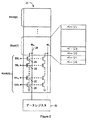
図1のフラッシュメモリ10のメモリセルアレイ18は、特定のフラッシュデバイスについて選択された設計パラメータである、任意の数のバンクからなる。図2は、図1のメモリセルアレイ18の1つのバンク20の編成を示す略図である。バンク20は、ブロック(Block[0]からBlock[k])として編成され、各ブロックは、ページ(WL0からWLi)からなる。kとiはどちらも、ゼロでない整数値である。各ページは、共通ワード線に結合されたメモリセルの行に対応する。ブロックのメモリセルの詳細な説明が次に行われる。
The
各ブロックは、直列結合で配置され、互いに電気的に結合されたフラッシュメモリセル22を有するNANDメモリセルストリングからなる。したがって、ワード線WL0からWLiは、メモリセルストリング内の各フラッシュメモリセルのゲートに結合される。信号SSL(ストリング選択線)に結合されたストリング選択デバイス24が、ビット線26にメモリセルストリングを選択的に接続し、信号GSL(グランド選択線)に結合されたグランド選択デバイス28が、VSSなどのソース線にメモリセルストリングを選択的に接続する。ストリング選択デバイス24およびグランド選択デバイス28は、nチャネルトランジスタである。
Each block consists of a NAND memory cell string having
ビット線26(BL0からBLj、ただしjはゼロでない整数値)は、バンク20のすべてのブロックに対して共通であり、各ビット線26は、ブロック[0]から[k]のそれぞれの中の1つのNANDメモリセルストリングに結合される。各ワード線(WL0からWLi)、SSL信号、およびGSL信号は、ブロック内の各NANDメモリセルストリング内の対応する同一のトランジスタデバイスに結合される。当業者には知られているように、1つのワード線に沿ったフラッシュメモリセル内に格納されたデータがデータのページと呼ばれる。
Bit lines 26 (BL 0 to BL j , where j is a non-zero integer value) are common to all blocks in
バンク20の外側で、フラッシュメモリセルの1ページ内にプログラムすべき書込みデータの1ページを格納するデータレジスタ30が、各ビット線に結合される。データレジスタ30はまた、フラッシュメモリセルの1ページから読み取られたデータを検知する検知回路をも含む。プログラミング動作中に、データレジスタは、プログラム検証動作を実行して、選択されたワード線に結合されたフラッシュメモリセル内にデータが適切にプログラミングされたことを保証する。高密度を達成するために、各フラッシュメモリセルは、少なくとも2ビットのデータを格納し、一般にはマルチビットセル(MBC)と呼ばれる。
Outside the
MBCフラッシュメモリに伴う問題は、そのメモリセルの、プログラム外乱に対する感度であることを当業者は理解する。プログラム外乱は、隣接するワード線と浮遊ゲートとの間の容量結合の結果として生じ、隣接するワード線と浮遊ゲートは、各製造技術世代に伴って互いに対してより近接して形成される。したがって、プログラミング中にあるセルに対して印加される高電圧が、隣接するセルのプログラムしきい電圧を、異なる論理状態を表すプログラムしきい電圧にシフトする可能性があり、あるセルのプログラム状態が、現在プログラムされている隣接するセルのしきい電圧に影響を及ぼす可能性がある。MBCフラッシュメモリ内のプログラム外乱を最小限に抑えるために、ブロック内のプログラミングは、WL0に対応するページで開始し、WLiまで順次進むことになる。あるいは、プログラミングは、WLiで開始し、WL0まで下に順次進むこともできる。NAND MBCフラッシュメモリセルをプログラミングするこうしたスキームは、当業界で周知である。ブロックがデータで完全にプログラムされると、次のファイルまたはデータの組のプログラミングが、次のブロックのWL0で開始する。デバイス内では、ブロックは通常、順次プログラムされる。 One skilled in the art understands that the problem with MBC flash memory is the sensitivity of the memory cell to program disturbances. Program disturb occurs as a result of capacitive coupling between adjacent word lines and floating gates, which are formed closer to each other with each manufacturing technology generation. Thus, a high voltage applied to a cell during programming can shift the programming threshold voltage of an adjacent cell to a programming threshold voltage that represents a different logic state, and the programming state of a cell May affect the threshold voltage of adjacent cells that are currently programmed. In order to minimize program disturbances in the MBC flash memory, the programming in the block will start on the page corresponding to WL 0 and proceed sequentially to WL i . Alternatively, programming can start at WL i and proceed down to WL 0 sequentially. Such schemes for programming NAND MBC flash memory cells are well known in the art. When the block is fully programmed with data, a set of programming of the next file or data, starting at WL 0 of the next block. Within a device, blocks are typically programmed sequentially.
フラッシュメモリ装置は、もはやデータを確実に格納するのに使用することができなくなるまでの消去-プログラムサイクルの数が限られていることが知られている。より具体的には、フラッシュメモリセルは、累積的なプログラム動作および消去動作によるフラッシュメモリセルの漸進的劣化であるプログラム/消去サイクル磨耗の対象となる。メモリブロックは、データでプログラムされる前に常にまず消去され、したがってサイクルをプログラムサイクルと消去サイクルの両方と呼ぶことができることを当業者は理解する。現在周知のすべてのフラッシュメモリは、ブロック消去のために構成され、そのことは、ブロック内のデータの1ページだけを修正/更新すべき場合、そのページを含むブロック全体が消去され、修正後のページおよび未修正のページで再プログラムされることを意味する。そのような累積的なプログラム動作および消去動作の効果は、最適なパラメータを超える、メモリセルのプログラム特性および消去特性の変質である。メモリセルが劣化したとき、メモリセルを所望のしきい電圧にプログラムまたは消去するのに、より高いプログラム電圧および消去電圧が必要となる。最終的に、メモリセルは、プログラムしきい電圧として表されるデータを適切に保持することに失敗する。例えば、MBCフラッシュメモリに関する典型的な消去-プログラムサイクルは、約10,000サイクルである。 Flash memory devices are known to have a limited number of erase-program cycles before they can no longer be used to reliably store data. More specifically, flash memory cells are subject to program / erase cycle wear, which is a gradual degradation of flash memory cells due to cumulative program and erase operations. Those skilled in the art will appreciate that a memory block is always first erased before being programmed with data, and thus a cycle can be referred to as both a program cycle and an erase cycle. All currently known flash memories are configured for block erase, which means that if only one page of data in a block is to be modified / updated, the entire block containing that page will be erased and the modified It means that it will be reprogrammed with pages and unmodified pages. The effect of such cumulative program and erase operations is a change in program and erase characteristics of the memory cell that exceeds optimal parameters. As the memory cell degrades, higher program and erase voltages are required to program or erase the memory cell to the desired threshold voltage. Eventually, the memory cell fails to properly hold the data expressed as the programmed threshold voltage. For example, a typical erase-program cycle for MBC flash memory is about 10,000 cycles.
現在、入手可能なほとんどのフラッシュメモリは、そのチップサイズに比べて記憶密度が高いために、MBCタイプのものである。MBCタイプはほとんどの消費者応用例に適しているが、10,000サイクルのプログラム-消去限界は、データのプログラミングおよび消去が頻繁な他の応用例にとって十分ではないことがある。したがって、MBCフラッシュメモリがその10,000サイクルの寿命に達したとき、MBCフラッシュメモリはもはや使用不能であり、廃棄しなければならない。この問題は、より頻繁なプログラム-消去サイクルがあるHDD応用例などの商用応用例にとって、より重大である。HDD応用例は、ほとんどの消費者応用例よりも高いデータ保全性を必要とするので、MBCフラッシュメモリの比較的短い10,000サイクルという寿命のために、MBCフラッシュメモリは使用に適さない。 Most flash memories currently available are of the MBC type because of their higher storage density compared to their chip size. Although the MBC type is suitable for most consumer applications, the 10,000 cycle program-erase limit may not be sufficient for other applications where data programming and erasure is frequent. Thus, when an MBC flash memory reaches its 10,000 cycle life, the MBC flash memory is no longer usable and must be discarded. This problem is more serious for commercial applications such as HDD applications with more frequent program-erase cycles. Because HDD applications require higher data integrity than most consumer applications, MBC flash memory is not suitable for use due to the relatively short lifetime of 10,000 cycles of MBC flash memory.
この問題は、フラッシュメモリ装置のブロックサイズが引き続き増加すると共に、格納されるデータファイルサイズが比較的静的なままであることによって悪化する。例えば、今日の高密度フラッシュデバイスに関するブロックサイズは256KBの範囲であるが、将来の高密度フラッシュデバイスは、512KBに近いブロックサイズを有することになる。ブロック内に格納されるデータファイルが小さい場合、データファイルが修正されるとき、ブロックがサイズを有するのと比べて、より多くのメモリセルが不必要に消去/プログラムサイクルの対象となることになる。 This problem is exacerbated by the fact that the block size of flash memory devices continues to increase and the data file size stored remains relatively static. For example, the block size for today's high density flash devices is in the range of 256 KB, but future high density flash devices will have a block size close to 512 KB. If the data file stored in the block is small, when the data file is modified, more memory cells will be subject to unnecessary erase / program cycles than the block has size. .
したがって、寿命が延長されるように動作可能なフラッシュメモリ装置を提供することが望ましい。 Accordingly, it is desirable to provide a flash memory device that is operable to extend its lifetime.
本実施形態の一態様は、従来のフラッシュメモリシステムの少なくとも1つの欠点を回避または軽減することである。 One aspect of this embodiment is to avoid or mitigate at least one drawback of conventional flash memory systems.
第1の態様では、メモリアレイおよび行回路を有するフラッシュメモリ装置が提供される。メモリアレイは、列として配置されたNANDフラッシュメモリセルストリングの少なくとも1つのブロックを有し、その少なくとも1つのブロックは、選択的に消去可能である、事前設定された数のフラッシュメモリセルを有する。事前設定された数のフラッシュメモリセルを消去するために基板に消去電圧までバイアスがかけられると、行回路は、事前設定された数のフラッシュメモリセルに対応する第1ワード線を第1電圧まで駆動する。第2ワード線に結合されたフラッシュメモリセルの消去を抑制するために、行デコーダが、第2ワード線を第2電圧まで駆動する。第1の態様の実施形態によれば、事前設定された数のフラッシュメモリセルは、マルチビットセル(MBC)でよく、フラッシュメモリセルの1つの順次セットに対応することができ、またはフラッシュメモリセルの2つの順次セットに対応することができ、この場合、フラッシュメモリの2つの順次セットは、互いに隣接しない。本態様の別の実施形態では、少なくとも1つのブロックのNANDフラッシュメモリセルストリングが、共通ソース線に結合され、フラッシュメモリ装置は、消去検証動作中に共通ソース線の電圧を第3電圧と第4電圧の間に設定するソース線電圧制御回路をさらに含む。第4電圧は第3電圧未満であり、共通ソース線の電圧は、第1ワード線の数が増加するにつれて下降する。 In a first aspect, a flash memory device having a memory array and a row circuit is provided. The memory array has at least one block of NAND flash memory cell strings arranged as columns, the at least one block having a preset number of flash memory cells that are selectively erasable. When the substrate is biased to the erase voltage to erase the preset number of flash memory cells, the row circuit will connect the first word line corresponding to the preset number of flash memory cells to the first voltage. To drive. A row decoder drives the second word line to a second voltage to suppress erasure of flash memory cells coupled to the second word line. According to an embodiment of the first aspect, the pre-set number of flash memory cells may be multi-bit cells (MBC) and may correspond to one sequential set of flash memory cells, or of flash memory cells Two sequential sets can be accommodated, in which case the two sequential sets of flash memory are not adjacent to each other. In another embodiment of the present aspect, at least one block of NAND flash memory cell strings is coupled to a common source line, and the flash memory device uses a third voltage and a fourth voltage on the common source line during an erase verify operation. A source line voltage control circuit that is set between the voltages is further included. The fourth voltage is less than the third voltage, and the voltage of the common source line decreases as the number of first word lines increases.
第2の態様では、メモリブロックのサブブロックを消去する方法であって、メモリブロックが、第1ワード線、最終ワード線、ならびに第1ワード線と最終ワード線との間の中間ワード線に結合されたNANDメモリセルストリングを有する方法が提供される。この方法は、第1アドレスを有する第1入力アドレスコマンドを発行すること、第2アドレスを有する第2入力アドレスコマンドを発行すること、部分消去コマンドを発行すること、および第1アドレスおよび第2アドレスに対応するワード線によってバインドされるワード線の組を有するサブブロックを消去することを含む。 In a second aspect, a method of erasing a sub-block of a memory block, wherein the memory block is coupled to a first word line, a last word line, and an intermediate word line between the first word line and the last word line A method having a NAND memory cell string formed is provided. The method includes issuing a first input address command having a first address, issuing a second input address command having a second address, issuing a partial erase command, and a first address and a second address Erasing a sub-block having a set of word lines bound by a word line corresponding to.
本態様の一実施形態によれば、第1アドレスはヌルアドレスを含み、サブブロックは、第2アドレスに対応する1つのワード線および第1ワード線によってバインドされるワード線の組を含む。本態様の別の実施形態では、第2アドレスはヌルアドレスを含み、サブブロックは、第1アドレスに対応する1つのワード線および最終ワード線によってバインドされるワード線の組を含む。さらに別の実施形態では、この方法は、消去されたサブブロックを消去検証することをさらに含む。消去検証することは、ビット線を事前充電すること、ワード線の組にバイアスをかけること、非選択ワード線にバイアスをかけること、および検知することを含む。事前充電するステップは、NANDメモリセルストリングに結合されたビット線を事前充電電圧レベルまで事前充電することを含む。ワード線の組に結合された消去済みメモリセルをオンにするために、ワード線の組に第1電圧までバイアスがかけられる。非選択ワード線に結合されたメモリセルをオンにするために、非選択ワード線に第2電圧までバイアスがかけられる。検知することは、事前充電電圧レベルの変化を検知することを含む。 According to one embodiment of the present aspect, the first address includes a null address, and the sub-block includes one word line corresponding to the second address and a set of word lines bound by the first word line. In another embodiment of this aspect, the second address includes a null address, and the sub-block includes a set of word lines bound by one word line and the last word line corresponding to the first address. In yet another embodiment, the method further includes erasing verifying the erased sub-block. Erase verify includes precharging the bit lines, biasing a set of word lines, biasing unselected word lines, and sensing. Precharging includes precharging a bit line coupled to the NAND memory cell string to a precharge voltage level. In order to turn on the erased memory cells coupled to the word line set, the word line set is biased to a first voltage. In order to turn on the memory cell coupled to the unselected word line, the unselected word line is biased to a second voltage. Detecting includes detecting a change in the precharge voltage level.
さらに別の実施形態では、第1電圧は負電圧であり、第2電圧は、読取り動作中に使用される読取り電圧である。あるいは、第1電圧は0Vでもよく、第2電圧は、読取り動作中に使用される読取り電圧である。別の実施形態では、NANDメモリセルストリングに結合された共通ソース線に可変ソースバイアス電圧までバイアスがかけられ、可変ソースバイアス電圧は、ワード線の組の数が減少するにつれて0Vから最大電圧まで上昇する。 In yet another embodiment, the first voltage is a negative voltage and the second voltage is a read voltage used during a read operation. Alternatively, the first voltage may be 0V and the second voltage is a read voltage used during a read operation. In another embodiment, the common source line coupled to the NAND memory cell string is biased to a variable source bias voltage that increases from 0V to the maximum voltage as the number of word line pairs decreases. To do.
第3の態様では、メモリブロックのサブブロック内のデータを修正するときの磨耗レベリング制御のための方法が提供される。この方法は、新しいメモリブロックの空きサブブロックに対して修正後データをプログラムすること、およびメモリブロックのサブブロックを消去することを含む。一実施形態では、この方法は、利用可能な最低ランキングのサブブロックに対して新しいデータをプログラムすることをさらに含み、各メモリブロックは、少なくとも2つのサブブロックを含み、利用可能な最低ランキングのサブブロックは、順次プログラミングスキームでプログラムすべき第1ワード線に最も近接するワード線の組を含む。別の実施形態では、この方法は、アドレスマッピングテーブルを更新し、修正後データの論理アドレスを新しいメモリブロックの空きサブブロックに対応する物理アドレスにマッピングすることを含む。さらに別の実施形態では、空きサブブロックは、利用可能な最低ランキングのサブブロックであり、またはサブブロックに等しいランキングを有する。空きサブブロックのランキングがサブブロックに等しいとき、新しいメモリブロックは空であり、または空きサブブロックよりも低いランキングを有する別のサブブロック内に格納された他のデータを含む。あるいは、空きサブブロックは、サブブロックよりも高いランキングを有する。さらに別の実施形態では、この方法は、サブブロックとメモリブロックの他の1つのサブブロックのプログラム/消去サイクル間の差が所定の値に達したとき、サブブロック内のデータを、他の1つのサブブロック内の他のデータとスワップすることを含む。 In a third aspect, a method is provided for wear leveling control when modifying data in a sub-block of a memory block. The method includes programming the modified data into an empty sub-block of a new memory block and erasing the sub-block of the memory block. In one embodiment, the method further includes programming new data for the lowest ranking sub-block available, each memory block including at least two sub-blocks, and the lowest ranking sub-block available. The block includes a set of word lines closest to the first word line to be programmed with a sequential programming scheme. In another embodiment, the method includes updating the address mapping table and mapping the logical address of the modified data to a physical address corresponding to a free sub-block of the new memory block. In yet another embodiment, the free sub-block is the lowest ranking sub-block available or has a ranking equal to the sub-block. When the ranking of the empty subblock is equal to the subblock, the new memory block is empty or contains other data stored in another subblock that has a lower ranking than the empty subblock. Alternatively, the empty subblock has a higher ranking than the subblock. In yet another embodiment, the method includes transferring data in a subblock to another one when the difference between the program / erase cycles of the subblock and one other subblock of the memory block reaches a predetermined value. Including swapping with other data in one sub-block.
特定の実施形態についての以下の説明を添付の図と共に検討することにより、本願発明の実施形態の他の態様および特徴が当業者には明らかとなる。 Other aspects and features of embodiments of the present invention will become apparent to those skilled in the art upon review of the following description of specific embodiments in conjunction with the accompanying figures.
これから、添付の図を参照しながら、単なる例示として実施形態を説明する。 Embodiments will now be described by way of example only with reference to the accompanying figures.
一般に、この実施形態は、フラッシュメモリデバイスの寿命を向上させる方法およびシステムを提供する。フラッシュメモリ装置の各物理メモリブロックは、少なくとも2つの論理サブブロックに分割可能であり、その少なくとも2つの論理サブブロックのそれぞれは消去可能である。したがって、論理ブロックのデータのみが消去および再プログラムされ、他の論理ブロック内の未修正データは、不要なプログラム/消去サイクルを回避する。消去すべき論理サブブロックは、サイズおよびブロック内の位置の点で動的に構成可能である。メモリアレイの物理サブブロックおよび論理サブブロック全体にわたってデータを配布するのに磨耗レベリングアルゴリズムが使用され、物理ブロックの寿命が最大にされる。 In general, this embodiment provides a method and system for improving the lifetime of a flash memory device. Each physical memory block of the flash memory device can be divided into at least two logical sub-blocks, and each of the at least two logical sub-blocks can be erased. Thus, only the data in the logical block is erased and reprogrammed, and unmodified data in other logical blocks avoids unnecessary program / erase cycles. The logical sub-block to be erased can be dynamically configured in terms of size and position within the block. A wear leveling algorithm is used to distribute data across the physical and logical sub-blocks of the memory array to maximize the lifetime of the physical block.
図3は、本実施形態による、フラッシュメモリ装置の物理メモリブロック(Block[0]からBlock[k])の概念図である。各物理ブロックは、選択的に消去される論理サブブロックを有することができ、消去されているサブブロックは、任意の数のページからなることができる。図3では、データを格納するメモリブロックの部分が、網掛けで示されており、メモリブロックの消去済みサブブロックは、網掛けを有さない。選択的に消去されているサブブロックのサイズを、物理ブロックの任意の比率となるように事前設定することができ、または実行中に動的に構成可能でよい。図3の例では、Block[0]は、Block[1]よりも小さい消去済みサブブロックを有する。物理ブロックサイズに応じて、例えば4つの論理サブブロックなどの、3つ以上の論理サブブロックに物理ブロックを分割することが好都合であることがある。したがって、各物理ブロックは、部分的に消去可能である。各物理ブロックのメモリセルが、図2に示されるようにNANDメモリセルストリングとして構成され、各ページがWL0からWLiの方向に順次プログラムされると仮定する。ただし、WLiは、プログラムすべき最後のワード線である。 FIG. 3 is a conceptual diagram of physical memory blocks (Block [0] to Block [k]) of the flash memory device according to the present embodiment. Each physical block can have logical sub-blocks that are selectively erased, and the erased sub-block can consist of any number of pages. In FIG. 3, the portion of the memory block that stores data is shown by shading, and the erased sub-block of the memory block has no shading. The size of the sub-blocks that are selectively erased can be preset to be an arbitrary ratio of physical blocks, or can be dynamically configurable during execution. In the example of FIG. 3, Block [0] has an erased sub-block smaller than Block [1]. Depending on the physical block size, it may be advantageous to divide the physical block into more than two logical sub-blocks, for example four logical sub-blocks. Therefore, each physical block can be partially erased. Assume the memory cells of each physical block is configured as a NAND memory cell string, as shown in FIG. 2, each page is sequentially programmed from WL 0 in the direction of WL i. WL i is the last word line to be programmed.
データがWL0からWLiまで順次プログラムされるこの例では、下位サブブロックと上位サブブロックがある。下位サブブロックは、ワード線の下位の順次セットを含み、上位サブブロックは、ワード線の上位の順次セットを含む。プログラム外乱を最小限に抑えるために、任意のメモリブロックの上位サブブロックが消去および再プログラムされ、下位サブブロックのデータが保持される。このスキームは、以前に消去された物理ブロックが一定のページまで順次プログラムされ、残りのページが消去された状態のままにされる状況に似ている。したがって、消去済み上位サブブロックまでデータが後で順次プログラムされるときに、プログラム外乱が最小限に抑えられる。下位サブブロックを消去することができると共に、データが隣接する上位サブブロック内に保持されるが、隣接する上位サブブロックが消去されるまで、下位サブブロックに対してデータを再プログラムすべきではない。 In this example, where data is programmed sequentially from WL 0 to WL i, there are lower and upper sub-blocks. The lower sub-block includes a lower sequential set of word lines, and the upper sub-block includes an upper sequential set of word lines. In order to minimize program disturbance, the upper subblock of any memory block is erased and reprogrammed to retain the data of the lower subblock. This scheme is similar to the situation where previously erased physical blocks are sequentially programmed to a certain page and the remaining pages remain erased. Thus, program disturbance is minimized when data is sequentially programmed up to the erased upper sub-block. The lower subblock can be erased and the data is retained in the adjacent upper subblock, but the data should not be reprogrammed to the lower subblock until the adjacent upper subblock is erased .
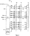
物理ブロックを部分的に消去するための一般的概念が導入されたので、それ以上の詳細な実施形態が、図4を参照しながら説明される。図4は、フラッシュメモリアレイ、ワード線ドライバブロック102、およびソース線電圧制御回路104の物理ブロック100を示す回路図である。ワード線ドライバブロック102およびソース線電圧制御回路104は通常、物理ブロック100に対してローカルなものである。物理ブロック100は、列として配置されたNANDフラッシュメモリセルストリングを有し、各ストリングは、ビット線BL0からBLj、共通ソース線CSLに結合される。ワード線ドライバブロック102は、信号SSをSSL制御線に、S[0:n]をWL0ワード線からWLnワード線にそれぞれ結合し、GSをGSL制御線に結合する。当業者には周知の通り、信号SS、S[0:n]、およびGSLは、プログラム中、プログラム検証中、読取り動作中、および消去動作中に異なる電圧レベルに設定される。ソース線電圧制御回路104は、実行中の前述の動作のうちの1つに応じて、CSLの電圧レベルを設定する任を担う。
Since the general concept for partially erasing a physical block has been introduced, a more detailed embodiment will be described with reference to FIG. FIG. 4 is a circuit diagram showing the
以下は、物理ブロック100の消去可能サブブロックの論理構成を示すための例示的シナリオである。物理ブロック100のすべてのページ(WL0からWLn)が、WL0からWLnの方向にデータでプログラムされており、WL27からWLnに結合されたメモリセル内に格納されたデータを修正すべきであると仮定する。したがって、ワード線WL27からWLnに結合されたメモリセル内に格納されたデータのみを消去するように、ビット線、ワード線WL27からWLn、およびソース線CSLにバイアスがかけられる。次いで、修正後データが、同じワード線に対して再プログラムされる。ワード線WL27からWLnに対応するページは、上位サブブロック106と呼ばれ、WL0からWL26に対応するページは、下位サブブロック108と呼ばれる。したがって、上位サブブロック106のサイズは、消去されるデータに依存するので、上位サブブロック106は、サイズの点で動的に構成可能である。あるいは、サブブロック106およびサブブロック108のサイズを固定することもできる。
The following is an exemplary scenario to illustrate the logical configuration of the erasable sub-block of
サブブロックが消去された後に、データを必ずしも再プログラムしなければならないわけではないので、現在説明している実施形態は、サブブロックの消去および再プログラムに限定されない。このことは、サブブロックがある動作で消去されると、消去されたサブブロックの下の任意の数の順次ページを後の動作で消去することができ、それによって、消去されるサブブロックのサイズが拡張されることを意味する。 Since the data does not necessarily have to be reprogrammed after the subblock has been erased, the presently described embodiments are not limited to subblock erasure and reprogramming. This means that if a sub-block is erased in one operation, any number of sequential pages under the erased sub-block can be erased in a later operation, thereby erasing the size of the sub-block to be erased Means that will be expanded.
前述のように、物理ブロックの特定のページが、ビット線、選択されたワード線および非選択ワード線、ならびにソース線にバイアスをかけることによって消去される。表1および2は、選択された物理ブロック内のページのサブブロックを消去するのに有効な例示的バイアス条件と、非選択物理ブロック内の消去を抑制するのに有効なバイアス条件とを与えるものである。 As described above, a particular page of the physical block is erased by biasing the bit lines, selected and unselected word lines, and source lines. Tables 1 and 2 provide exemplary bias conditions that are effective for erasing sub-blocks of pages in the selected physical block and bias conditions that are effective for suppressing erasure in unselected physical blocks. It is.

表1の例では、非選択ワード線に正電圧のバイアスがかけられ、対応する非選択ページ(複数可)が消去されることが防止される。この電圧はVersと呼ばれる。選択されたワード線に別の電圧、例えば0Vのバイアスがかけられ、選択されたページ(複数化)が消去される。Versなどの正電圧までバイアスがかけられたメモリセルの基板では、0Vまでバイアスがかけられたメモリセルと基板との間に電界が形成され、この電界は、メモリセルを消去するのに有効である。Versまでバイアスがかけられたメモリセルと基板との間の電場は、メモリセルを消去するのには不十分であり、したがって消去が抑制され、メモリセル内に格納されたデータが保持される。 In the example of Table 1, a non-selected word line is biased with a positive voltage, preventing the corresponding unselected page (s) from being erased. This voltage is called Vers. The selected word line is biased with another voltage, for example, 0V, and the selected page (multiple) is erased. In a memory cell substrate biased to a positive voltage such as Vers, an electric field is formed between the memory cell biased to 0 V and the substrate, and this electric field is effective for erasing the memory cell. is there. The electric field between the memory cell biased to Vers and the substrate is insufficient to erase the memory cell, and therefore erasure is suppressed and the data stored in the memory cell is retained.
非選択ブロック内のメモリセルの消去を防止するために、非選択ブロック内のすべてのワード線が、消去動作中に浮遊するままにされる。非選択ブロック内の浮遊するワード線は、ほぼ消去電圧Versまで昇圧され、セルアレイの基板にVersまでバイアスがかけられたときに、Versが基板に印加されたときの基板とワード線との間の容量結合により、Versの約90%となることができる。浮遊ワード線上の実際の昇圧電圧レベルは、基板とワード線との間の結合率によって決定されることに留意されたい。非選択ブロック内のワード線上の昇圧電圧は、基板とワード線との間の電界を低減し、それによってメモリセルの消去が抑制される。フラッシュメモリ内のワード線昇圧のより詳しい詳細が、本願と同じ所有者の2006年11月30日出願の米国特許出願第11/565,170号に記載されている。 To prevent erasure of memory cells in the unselected block, all word lines in the unselected block are left floating during the erase operation. The floating word line in the unselected block is boosted to approximately the erase voltage Vers, and when the cell array substrate is biased to Vers, the Vers is applied between the substrate and the word line when applied to the substrate. Capacitive coupling can be about 90% of Vers. Note that the actual boosted voltage level on the floating word line is determined by the coupling rate between the substrate and the word line. The boosted voltage on the word line in the unselected block reduces the electric field between the substrate and the word line, thereby suppressing erasure of the memory cell. More detailed details of boosting word lines in flash memory are described in US patent application Ser. No. 11 / 565,170 filed Nov. 30, 2006, which is the same owner as the present application.
表2の例では、バイアス条件は、選択されたブロックの非選択ワード線がほぼ消去電圧Versまで昇圧されることを除いて、表1に示されるものと同一である。一実施形態では、この昇圧電圧はVersの約90%であり、これは、ビット線およびソース線を通じてメモリセルを事前充電し、基板がVersまで上昇するときに基板に対する容量結合を通じてワード線を昇圧することによって達成される。この場合も、消去を抑制するためのワード線昇圧の詳細が、米国特許出願第11/565,170号に詳細に記載されている。表1および2に示される、例示されるバイアス条件は例に過ぎないが、特定の値が製造工程、使用される材料、メモリセルの特定の設計に依存することを当業者は理解することができる。 In the example of Table 2, the bias conditions are the same as those shown in Table 1 except that the unselected word lines of the selected block are boosted to approximately the erase voltage Vers. In one embodiment, this boost voltage is approximately 90% of Vers, which precharges the memory cells through the bit and source lines and boosts the word line through capacitive coupling to the substrate as the substrate rises to Vers. Is achieved by doing Also in this case, the details of the word line boosting for suppressing erasure are described in detail in US patent application Ser. No. 11 / 565,170. The illustrated bias conditions shown in Tables 1 and 2 are only examples, but one skilled in the art will understand that the specific values depend on the manufacturing process, the materials used, and the specific design of the memory cell. it can.
物理ブロックのサブブロックが消去されると、データが再プログラムされる前に実行すべき任意選択の手続きは、消去検証動作である。消去検証動作は、消去されるセルが、しきい電圧に適切なしきい電圧マージンを有することを保証する。例えば、消去しきい電圧は、ある負電圧値となる。従来のブロック消去アーキテクチャでは、消去検証が、ブロックのすべてのワード線に0Vまでバイアスをかけ、NANDメモリセルストリングを通る電流を検知することによって実行される。0Vよりも高い消去しきい電圧を有する少なくとも1つのメモリセルを有するどんなメモリセルもオンされず、対応するビット線中の電流の欠如が検知される。この従来のスキームは、メモリセルの一部が多数の可能なしきい電圧のうちの1つに対応するデータを依然として保持するときには可能ではない。 When a sub-block of a physical block is erased, an optional procedure to be performed before data is reprogrammed is an erase verify operation. The erase verify operation ensures that the cells to be erased have a threshold voltage margin appropriate to the threshold voltage. For example, the erase threshold voltage is a certain negative voltage value. In conventional block erase architectures, erase verification is performed by biasing all word lines of the block to 0V and sensing the current through the NAND memory cell strings. Any memory cell having at least one memory cell with an erase threshold voltage higher than 0V is not turned on, and the lack of current in the corresponding bit line is detected. This conventional scheme is not possible when a portion of the memory cell still retains data corresponding to one of many possible threshold voltages.
一実施形態によれば、部分消去済みブロックのための消去検証動作が、消去されるメモリセルに結合された選択されるワード線に、消去しきい電圧よりも高い電圧までバイアスをかけ、残りのすべての非選択ワード線に、読取り動作のために使用される電圧までバイアスをかけることによって実行される。この電圧はVreadと呼ばれ、例えば4〜5Vの間で変化することができる。表3は、部分消去済みブロックに対する消去検証動作を実施するための例示的バイアス条件を示す。 According to one embodiment, an erase verify operation for a partially erased block biases the selected word line coupled to the memory cell to be erased to a voltage higher than the erase threshold voltage, and the remaining This is done by biasing all unselected word lines to the voltage used for the read operation. This voltage is called Vread and can vary, for example, between 4-5V. Table 3 shows exemplary bias conditions for performing an erase verify operation on a partially erased block.
一実施形態によれば、ソース線(Vcs)の電圧は、負のしきい値消去電圧が0Vから十分に離間することを保証するために、検証中のワード線の数に対して調節可能である。例えば、負のしきい値消去電圧が少なくとも-0.5Vであるべきであり、消去の結果、しきい値-0.2Vとなる場合、-0.2Vのしきい値を検出するために、ワード線に-0.5Vまでバイアスをかけるべきである。しかし、負の電圧はあるデバイスでは使用に適さないことがあるので、ソース線Vcsが正電圧レベルまで上げられ、選択されたワード線に0Vまでバイアスがかけられる。Vcsに正のバイアスをかけることにより、選択されたワード線は実質的に負となる。当業者はこの効果を理解するはずである。 According to one embodiment, the voltage on the source line (Vcs) can be adjusted with respect to the number of word lines being verified to ensure that the negative threshold erase voltage is well separated from 0V. is there. For example, if the negative threshold erase voltage should be at least -0.5V and the erase results in a threshold of -0.2V, the word line can be detected to detect a threshold of -0.2V. Should be biased to -0.5V. However, since negative voltages may not be suitable for use in certain devices, the source line Vcs is raised to a positive voltage level and the selected word line is biased to 0V. By applying a positive bias to Vcs, the selected word line becomes substantially negative. One skilled in the art should understand this effect.
図5は、ソース線電圧と、検証中の消去されたサブブロックに対応する、選択されたワード線の数との間の関係を示す。x軸は、検証すべきワード線の合計数であり、y軸は、共通ソース線の電圧(Vcs)である。斜め曲線120は、Vcsの電圧レベルと、選択されたワード線の数との間の理想的な関係を表す。Vcs電圧は、検証すべき、選択されたワード線の数が増加するにつれて低下することが明らかである。ただ1つのワード線を検証すべき場合、Vcsを例えば0.4Vなどの第1電圧に設定することができる。他方の極限では、すべてのワード線を検証すべき場合、Vcsを、第2のより低い電圧0Vに設定することができる。したがって、ここで示される実施形態でのVcsの範囲は、0Vから0.4Vの間で変化することができる。各NANDメモリセルストリング内により多くのワード線を有する代替実施形態では、0.4Vよりも高い電圧を使用することができる。
FIG. 5 shows the relationship between the source line voltage and the number of selected word lines corresponding to the erased sub-block under verification. The x-axis is the total number of word lines to be verified, and the y-axis is the common source line voltage (Vcs). The
斜め曲線120は理想的であるが、少なくともいくつかの実施例でそれを実施するのに必要な細かい制御は、非現実的である。しかし、当業者は理解するであろうが、選択されたワード線のグルーピングに対する階段形電圧をソース線電圧制御回路104で現実的に実施することができる。階段形曲線122は、可能であるステップサイズおよびワード線グルーピングの一例を示す。第1電圧、第2電圧、ワード線グルーピングのサイズ、およびグルーピング間の電圧ステップサイズの選択は、フラッシュメモリ装置の設計パラメータに基づくことになる。
The
次に、図6を参照しながら、部分ブロック消去および消去検証方法実施形態が説明される。各部分ブロック消去動作について、図6の方法を実行することができる。この方法は、ステップ200で、ERS_LOOPと呼ばれる消去ループカウンタ変数を1または任意の所望の開始値に等しく設定することによって開始する。ステップ202で、NANDメモリセルストリング内の少なくとも1つのメモリセルを消去するために、部分ブロック消去動作が実行される。このステップは、部分消去命令を受け取ること、消去すべきメモリセル(複数可)に対応するアドレス(複数可)を受け取ること、選択されたワード線(複数可)、非選択ワード線(複数可)、ビット線、および他の関連する信号に、選択されたワード線に結合されたメモリセルを消去するのに十分なレベルまでバイアスをかけることを含む。先に示された表1および2は、使用することのできる例示的バイアス値を列挙する。
Next, with reference to FIG. 6, a partial block erase and erase verification method embodiment will be described. For each partial block erase operation, the method of FIG. 6 can be performed. The method begins at
次に、物理ブロックのサブブロックが部分的に消去された後に、ステップ204で消去検証シーケンスが開始する。このステップは、選択されたワード線の数に基づいて適切なVcsレベルを設定すること、および選択されたワード線に結合されたメモリセルの消去された状態を検知するために、選択されたワード線および非選択ワード線に適切な電圧でバイアスをかけることを含む。先に示された表3は、使用することのできる例示的バイアス値を列挙する。ビット線が事前充電され、ビット線の検知が開始される。ステップ206で、検知が完了し、結果は、部分消去動作が成功した、または成功しなかったことを示すことになる。例えば、選択されたワード線に0Vまでバイアスをかけ、非選択ワード線、SSL、およびGSLにVreadまでバイアスをかけることにより、選択されたワード線に結合されたすべてのメモリセルが0V未満のしきい電圧を有する場合、高電圧レベルまで事前充電された対応するビット線が、Vcsまで放電することになり、それによってテストに合格する。しかし、選択されたワード線に結合された少なくとも1つのメモリセルが0Vよりも高いしきい値を有する場合、ビット線はVcsまで放電されず、それによってテストに不合格となる。当業者には周知であるが、どちらのケースも、ビット線センス増幅器回路によって検出することができる。
Next, after the sub-blocks of the physical block are partially erased, the erase verification sequence starts at step 204. This step sets the appropriate Vcs level based on the number of selected word lines and detects the erased state of the memory cells coupled to the selected word line. Including biasing the lines and unselected word lines with appropriate voltages. Table 3 shown above lists exemplary bias values that can be used. The bit line is precharged and detection of the bit line is started. At
テストに不合格であった場合、方法はステップ208に進み、カウンタ変数ERS_LOOPが最大値Maxと比較され、現ループカウンタがMax未満である場合、ステップ210でERS_LOOPが増分される。ステップ210より、方法はステップ202に戻り、選択されたサブブロックの部分消去が反復される。2つの条件の一方が満たされるまで、部分消去ステップおよび検証ステップ202、204、206、208、および210が続行される。カウンタ変数ERS_LOOPが最大値Maxに達した場合、第1条件が生じ、その場合、方法はステップ212に進み、ステータスレジスタが更新され、消去不合格ステータスが反映される。あるいは、サブブロックに対応するすべてのページが、別の用途から設計される。次いで、方法はステップ214で終了する。テストに合格した場合、第2条件が生じ、その場合、方法はステップ206からステップ216に進み、ステータスレジスタが更新され、消去合格ステータスが反映される。次いで、このサブブロックは、新しいデータでプログラムされる準備ができる。
If the test fails, the method proceeds to step 208 where the counter variable ERS_LOOP is compared to the maximum value Max, and if the current loop counter is less than Max, step 210 increments ERS_LOOP. From
まとめると、図3から6に示される実施形態を参照しながら、部分消去の概念が全般的に説明された。メモリブロックを部分に消去することにより、フラッシュメモリ装置は、メモリブロック内にサブブロックと呼ばれるより小さなサブディビジョンを作成することができる。メモリブロック全体を消去する必要なしに、サブブロックを占有するデータを修正することができ、それによってプログラム/消去サイクルが温存され、メモリブロックの寿命が向上する。以下の説明は、どのように特定のサブブロックが消去すべきであるかと選択されるかを論じる。 In summary, the concept of partial erasure has been generally described with reference to the embodiments shown in FIGS. By erasing the memory block in part, the flash memory device can create smaller subdivisions called sub-blocks within the memory block. The data occupying the sub-block can be modified without having to erase the entire memory block, thereby preserving the program / erase cycle and improving the lifetime of the memory block. The following description discusses how a particular sub-block should be selected to be erased.
メモリブロックの何らかのサブブロックを消去すべきであるとき、フラッシュメモリ装置は、メモリブロック内のそのサブブロックの位置についての情報を必要とし、その結果、フラッシュメモリ装置は、バイアス電圧の印加のためにどの行(ワード線)を選択して、それに結合されたメモリセルの消去を実施するかを認識することになる。図7aから7cは、メモリブロック内の消去可能サブブロックの可能な3つのサイズ/位置を示す。 When any sub-block of a memory block is to be erased, the flash memory device needs information about the location of that sub-block within the memory block, so that the flash memory device can It will be recognized which row (word line) is selected to erase the memory cell coupled thereto. Figures 7a to 7c show three possible sizes / positions of erasable sub-blocks within the memory block.
図7aは、WL0からWL31まで順次プログラムされるNANDメモリセルストリングの回路図である。この実施形態では、フラッシュメモリ装置が必要とするのは、開始アドレスとしての1つのワード線アドレスだけである。開始アドレスが受信されると、フラッシュメモリ装置の論理回路が、サブブロックサイズを開始アドレスから最後のワード線、この例ではWL31までとなるように自動的に設定する。図7aを参照しながら例示するために、WL27に対応する開始アドレスが部分消去動作に関して受信された場合、フラッシュメモリ装置の論理回路は、サブブロック300がW27で開始し、WL31で終了することを決定する。言い換えれば、提供される開始アドレスの如何に関わらず、終了アドレスはWL31となるように事前設定される。サブブロック300に関するワード線の組が決定されると、選択されるワード線および非選択ワード線にバイアスをかけることにより、部分消去手続きおよび消去検証手続きを実行することができる。サブブロック300は上位サブブロックであり、上位サブブロックは、順次プログラムすべき最終ワード線を含むワード線の任意のグルーピングである。
Figure 7a is a circuit diagram of a NAND memory cell string sequentially programmed from WL 0 to WL 31. In this embodiment, the flash memory device requires only one word line address as a start address. When the start address is received, the logic circuit of the flash memory device automatically sets the sub-block size from the start address to the last word line, in this example, WL 31 . To illustrate with reference to FIG. 7a, if a start address corresponding to WL 27 is received for a partial erase operation, the logic circuit of the flash memory device starts with
図7bは、図7aのNANDメモリセルストリングの回路図である。図7aの実施形態と同様に、部分消去動作のために必要なのは1つの開始行アドレスだけである。この実施形態では、フラッシュメモリ装置の論理回路は、サブブロックサイズを、開始アドレスから下に第1ワード線WL0までであると自動的に設定することができる。図7bを参照しながら例示するために、WL26に対応する開始アドレスが部分消去動作に関して受信された場合、フラッシュメモリ装置の論理回路は、サブブロック302がW26で開始し、WL0で終了することを決定する。提供される開始アドレスの如何に関わらず、終了アドレスはWL0となるように事前設定される。サブブロック302は下位サブブロックであり、下位サブブロックは、順次プログラムすべき第1ワード線を含むワード線の任意のグルーピングである。
FIG. 7b is a circuit diagram of the NAND memory cell string of FIG. 7a. Similar to the embodiment of FIG. 7a, only one starting row address is required for the partial erase operation. In this embodiment, the logic circuit of the flash memory device can automatically set the sub-block size from the start address to the first word line WL 0 down. To illustrate with reference to FIG. 7b, when a start address corresponding to WL 26 is received for a partial erase operation, the logic circuit of the flash memory device starts with
図7aと7bの実施形態のどちらも、1つのメモリブロックを下位サブブロックと上位サブブロックに細分する。しかし、1つのサブブロックが消去され、データで部分的に再プログラムされるだけである場合、依然として消去された状態のページがあることになる。さらに、元のサブブロックの消去は、消去されたページにさらなる消去動作を施すことになり、これは望ましくない。したがって、図7cの実施形態に示されるように、サブブロックスライスを選択することができる。 Both the embodiments of FIGS. 7a and 7b subdivide one memory block into a lower sub-block and an upper sub-block. However, if one sub-block is erased and only partially reprogrammed with data, there will still be an erased page. Furthermore, erasing the original sub-block will result in a further erase operation on the erased page, which is undesirable. Thus, a sub-block slice can be selected as shown in the embodiment of FIG. 7c.
図7cは、図7aのNANDメモリセルストリングの回路図である。このとき、開始アドレスおよび終了アドレスは、メモリブロック内のサブブロック位置およびサイズを定義する。この実施形態では、フラッシュメモリ装置の論理回路は、サブブロックサイズを、開始アドレスから終了アドレスとなるように自動的に設定する。図7cを参照しながら例示するために、WL2に対応する開始アドレスおよびWL28に対応する終了アドレスが部分消去動作に関して受信された場合、フラッシュメモリ装置の論理回路は、サブブロックスライス304がWL2で開始し、WL28で終了することを決定する。サブブロックスライスは、NANDメモリセルストリングの他のワード線間に配置されたワード線の任意のグルーピングである。プログラム外乱を最小限に抑えるために、WL0およびWL1に対応するページ内に格納されたデータがある場合であっても、WL29からWL31に対応するページが消去されることを条件として、サブブロックスライス304を反復的に消去し、プログラムすることができる。
FIG. 7c is a circuit diagram of the NAND memory cell string of FIG. 7a. At this time, the start address and the end address define the sub-block position and size in the memory block. In this embodiment, the logic circuit of the flash memory device automatically sets the sub-block size from the start address to the end address. To illustrate with reference to FIG. 7c, if a start address corresponding to WL 2 and an end address corresponding to WL 28 are received for a partial erase operation, the logic circuit of the flash memory device will indicate that the
図7a〜7cに示されるように、上位サブブロックまたは下位サブブロックを消去するのに少なくとも1つのアドレスが使用され、サブブロックスライスを消去するのに2つのアドレスが使用される。一実施形態によれば、フラッシュメモリコントローラがフラッシュメモリ装置とインターフェースし、上位サブブロック、下位サブブロック、またはサブブロックスライスの消去を開始することを可能にするように、コマンドプロトコルが提供される。フラッシュメモリ装置(複数可)とコンピュータなどのホストシステムとの間のインターフェースとして働く単一のフラッシュメモリコントローラによって、1つまたは複数のフラッシュメモリ装置を制御できることを当業者は理解する。 As shown in FIGS. 7a-7c, at least one address is used to erase the upper or lower sub-block and two addresses are used to erase the sub-block slice. According to one embodiment, a command protocol is provided to allow the flash memory controller to interface with the flash memory device and initiate an erase of the upper sub-block, lower sub-block, or sub-block slice. Those skilled in the art will appreciate that one or more flash memory devices can be controlled by a single flash memory controller that serves as an interface between the flash memory device (s) and a host system such as a computer.
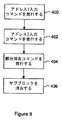
図8は、メモリブロックのサブブロックを消去するコマンドプロトコル実施形態を示すフローチャートである。図1の制御回路12で実装することのできるフラッシュメモリ制御論理が、このコマンドプロトコルに応答するように構成されると仮定する。メモリブロックに対して部分消去動作を実行するために、フラッシュメモリコントローラはまず、ステップ400で、第1アドレスを含むアドレス入力コマンドを発行する。それに続いてステップ402で、フラッシュメモリコントローラは、第2アドレスを含む別のアドレス入力コマンドを発行する。後でより詳細に説明するように、第1または第2アドレスはヌルアドレス値でよい。部分消去コマンドがステップ404で発行され、以前に受信された第1および第2アドレスに応じて、上位サブブロック、下位サブブロック、またはサブブロックスライスが、ステップ406で消去される。ステップ406で消去することは、ワード線、ビット線、およびソース線に、その適切な電圧レベルまでバイアスをかけることを含む。
FIG. 8 is a flowchart illustrating a command protocol embodiment for erasing a sub-block of a memory block. Assume that the flash memory control logic that can be implemented in the
このコマンドプロトコル例では、3つのアドレスの組合せが可能にされる。第1のケースでは、第1アドレスが有効であり、第2アドレスがヌルであるとき、制御論理は、第1アドレスに対応するワード線(NANDメモリセルチェーンの第1ワード線と最終ワード線の間の中間ワード線と呼ばれる)から、NANDメモリセルストリングの最終ワード線、この例ではWL31までによってバインドされ、それらを含む上位サブブロックを選択する。第2のケースでは、第1アドレスがヌルであり、第2アドレスが有効であるとき、制御論理は、第2アドレスに対応する中間ワード線から、NANDメモリセルストリングの第1ワード線、この例ではWL0までによってバインドされ、それらを含む下位サブブロックを選択する。第3のケースでは、第1および第2アドレスが有効であるとき、制御論理は、第1および第2アドレスに対応するワード線によってバインドされ、それらを含むサブブロックスライスを選択する。当業者は、上記で列挙された3つの状況が、可能な1つのプロトコル構成を表すことを理解する。一代替構成では、第1のケースの結果、下位サブブロックが選択され、第2のケースの結果、上位サブブロックが選択される。さらに別の代替実施形態では、第1および第2入力アドレスコマンドのいずれかが発行される前に、部分消去コマンドを発行することができる。 In this command protocol example, a combination of three addresses is allowed. In the first case, when the first address is valid and the second address is null, the control logic is responsible for the word line corresponding to the first address (the first word line and the last word line of the NAND memory cell chain). To the last word line of the NAND memory cell string, in this example up to WL 31 , to select the upper sub-block containing them. In the second case, when the first address is null and the second address is valid, the control logic begins with the first word line of the NAND memory cell string from the intermediate word line corresponding to the second address, in this example Now bind to WL 0 and select the sub-block that contains them. In the third case, when the first and second addresses are valid, the control logic is bound by the word lines corresponding to the first and second addresses and selects the sub-block slice containing them. One skilled in the art understands that the three situations listed above represent one possible protocol configuration. In an alternative configuration, the lower subblock is selected as a result of the first case, and the upper subblock is selected as a result of the second case. In yet another alternative embodiment, a partial erase command can be issued before any of the first and second input address commands are issued.
図9は、図8に示されるコマンドプロトコルを使用して、上位サブブロック、下位サブブロック、またはサブブロックスライスを消去する特定の方法実施形態のフローチャートである。より具体的には、上位サブブロック、下位サブブロック、およびサブブロックスライスのうちの1つが、第1入力アドレスコマンドおよび第2入力アドレスコマンドと共に受信された第1または第2有効アドレスの存在または欠如に基づいて消去される。以下の説明のために、フラッシュコントローラが、フラッシュメモリ装置のメモリブロックのサブブロックを消去する部分消去コマンドを発行するように構成され、フラッシュメモリ装置が、部分消去動作および消去検証動作のためにワード線、ビット線、および他の信号にバイアスをかける制御論理を含むと仮定する。 FIG. 9 is a flowchart of a particular method embodiment for erasing an upper subblock, lower subblock, or subblock slice using the command protocol shown in FIG. More specifically, the presence or absence of the first or second effective address received by one of the upper subblock, lower subblock, and subblock slice with the first input address command and the second input address command. Erased based on For purposes of the following discussion, the flash controller is configured to issue a partial erase command that erases a sub-block of a memory block of the flash memory device, and the flash memory device has a word for a partial erase operation and an erase verify operation. Assume that it contains control logic that biases lines, bit lines, and other signals.
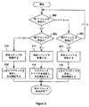
図9の方法は、図8のコマンドプロトコルによる、アドレス入力コマンドおよび消去コマンドに応答する、フラッシュメモリ装置制御論理の論理演算を示す。図9の方法はステップ500で開始し、第1アドレス入力コマンドが受信される。このアドレス入力コマンドは、メモリブロックのNANDメモリセルストリングのワード線に対応する第1有効アドレス、またはヌルアドレスを含む。第1のケースでは、第1アドレスは有効であり、方法はステップ502に進み、第2アドレス入力コマンドが第2アドレスと共に受信される。第2アドレスは、NANDメモリセルストリングの異なるワード線に対応する有効アドレス、またはヌルアドレスでよい。第1のケースを続けると、第2アドレスはヌルアドレスであり、方法はステップ504に進む。ステップ504で、部分消去コマンドが受信され、ステップ506で、上位サブブロックが消去され、検証される。ステップ504は、ワード線と、ビット線と、上位サブブロックを消去し、上位サブブロックを消去検証する他の関連信号の適切なバイアシングを含む。
The method of FIG. 9 illustrates a logical operation of the flash memory device control logic in response to an address input command and an erase command according to the command protocol of FIG. The method of FIG. 9 begins at
ステップ500に戻ると、第1アドレスが有効アドレスではなく、ヌルアドレスである場合、ステップ502と同一であるステップ508に進む。第2アドレスもヌルアドレスである場合、部分消去方法は終了し、ステップ500に戻る。一方、第2アドレスが有効アドレスである場合、ケース2が生じる。部分消去コマンドがステップ510で受信されると、ステップ512で、下位サブブロックが消去され、検証される。ステップ512は、ワード線と、ビット線と、下位サブブロックを消去し、下位サブブロックを消去検証する他の関連信号の適切なバイアシングを含む。ステップ502に戻ると、ステップ500からの第1アドレスが有効であり、かつ第2アドレスが有効である場合、ケース3が生じる。その場合、方法はステップ514に進み、部分消去コマンドが受信される。次いで、ステップ516で、サブブロックスライスが消去され、検証される。ステップ516は、ワード線と、ビット線と、サブブロックスライスを消去し、サブブロックスライスを消去検証する他の関連信号の適切なバイアシングを含む。
Returning to step 500, if the first address is not a valid address but a null address, the process proceeds to step 508, which is the same as
コマンドプロトコルは、ケース1では第2有効アドレスを必要とせず、またはケース2では第1有効アドレスを必要としないが、ケース1およびケース2について、それぞれ有効な第2アドレスおよび第1アドレスを受諾するようにコマンドプロトコルを構成することができる。例えば、上位サブブロックを消去するために、第1アドレスは中間ワード線に対応し、第2有効アドレスは例えば最終ワード線WL31に対応する。同様に、下位サブブロックを消去するために、第1アドレスは、第1ワード線WL0に対応し、第2有効アドレスは中間ワード線に対応する。
The command protocol does not require a second effective address in
したがって、図8および9に示されるコマンドプロトコルおよび方法を使用することにより、メモリアレイの他のサブブロック(複数可)のプログラム消去サイクル寿命に影響を及ぼすことなく、メモリブロックの任意のサブブロックを反復的に消去し、データで再プログラムすることができる。任意のサブブロックを消去するように構成された、1つまたは複数のフラッシュメモリ装置を有する任意のフラッシュメモリ装置またはフラッシュメモリシステムを制御して、メモリブロックの寿命を最大にする磨耗レベリングアルゴリズムを実行することができ、それによってフラッシュメモリ装置の寿命が最大となる。磨耗レベリングアルゴリズムなしに動作するフラッシュメモリ装置は、第1メモリブロックから最終メモリブロックまでデータを順次プログラムし、各メモリブロックを、次のメモリブロックをプログラムする前に満たす。システムが第1メモリブロックで継続的にデータをプログラムおよび消去し、他のメモリブロックを未使用のままにする場合、不均一な磨耗が生じることになる。 Therefore, by using the command protocol and method shown in FIGS. 8 and 9, any sub-block of a memory block can be moved without affecting the program erase cycle life of the other sub-block (s) of the memory array. It can be erased repeatedly and reprogrammed with data. Control any flash memory device or flash memory system with one or more flash memory devices configured to erase any sub-block to run a wear leveling algorithm that maximizes memory block life And thereby maximize the lifetime of the flash memory device. A flash memory device operating without a wear leveling algorithm sequentially programs data from a first memory block to a final memory block, filling each memory block before programming the next memory block. If the system continuously programs and erases data in the first memory block and leaves other memory blocks unused, uneven wear will occur.
磨耗レベリングは、フラッシュメモリ装置のすべてのメモリを均一に使用することを保証するスキームである。より具体的には、磨耗レベリングは、すべてのメモリブロックがほぼ同数のプログラムサイクルまたは消去サイクルを受けることを保証する。データがもはや確実に格納されなくなるまで、有限の回数だけフラッシュメモリセルをプログラム/消去できることを当業者は理解する。フラッシュコントローラは、メモリブロックの各メモリブロックまたはページが受けるプログラム/消去サイクルの合計数を追跡する。サイクル数は、メモリアレイの各ページのスペアフィールド内に格納される。フラッシュコントローラは、データの論理アドレス位置を、フラッシュメモリ装置内にデータが格納される物理アドレスにマッピングする。メモリブロックが所定の最大プログラム/消去サイクル数に達したとき、フラッシュコントローラは、利用可能なメモリブロックに、メモリブロック内に格納されたデータを再プログラムするようにフラッシュメモリ装置に指令し、次いで、元のメモリブロックを別の用途から設計する(ここでは無効ブロックと呼ばれる)。次いで、それに応じてマッピングが調節される。 Wear leveling is a scheme that ensures uniform use of all memory in a flash memory device. More specifically, wear leveling ensures that all memory blocks receive approximately the same number of program or erase cycles. Those skilled in the art will appreciate that flash memory cells can be programmed / erased a finite number of times until data is no longer reliably stored. The flash controller tracks the total number of program / erase cycles that each memory block or page of the memory block receives. The number of cycles is stored in the spare field of each page of the memory array. The flash controller maps the logical address position of the data to a physical address where the data is stored in the flash memory device. When the memory block reaches a predetermined maximum number of program / erase cycles, the flash controller instructs the available memory block to reprogram the data stored in the memory block, and then Design the original memory block for another use (referred to here as an invalid block). The mapping is then adjusted accordingly.
現在周知の磨耗レベリング技法は、異なるメモリブロックにわたってデータをプログラムするのに論理-物理マッピング技法を使用する。例えば、プログラムすべき大きいデータファイルが、第1ブロックに対してプログラムされた第1部分を有することができ、第2ブロックに対してプログラムされた第2部分を有することができ、以下同様である。別の例では、合計で1つのメモリブロックのサイズ未満である複数のデータファイルを、それぞれ異なるメモリブロックに対してプログラムすることができる。したがって、大きいデータファイルの特定の部分、または特定の小さいデータファイルを修正すべきである場合、それを格納する、対応するメモリブロックのみが、プログラム/消去サイクルの対象となる。これらのすべてのスキームに伴う問題は、メモリブロック内に存在する小さいデータファイルまたはデータファイルの一部を修正することがメモリブロック全体の消去を必要とすることである。したがって、メモリブロック内に格納された他のデータも消去され、修正後データが再プログラムされるときに不必要に再プログラムされることになる。これが、メモリブロックの寿命の低下に寄与する主な要因である。 Currently known wear leveling techniques use logical-physical mapping techniques to program data across different memory blocks. For example, a large data file to be programmed can have a first part programmed for the first block, can have a second part programmed for the second block, and so on. . In another example, a plurality of data files that total less than the size of one memory block can be programmed for different memory blocks. Thus, if a particular part of a large data file or a particular small data file is to be modified, only the corresponding memory block that stores it is subject to a program / erase cycle. The problem with all these schemes is that modifying a small data file or part of a data file that exists in a memory block requires erasing the entire memory block. Therefore, other data stored in the memory block is also erased and unnecessarily reprogrammed when the modified data is reprogrammed. This is a main factor that contributes to a reduction in the lifetime of the memory block.
前述の例示的実施形態では、消去すべきサブブロックは、消去または修正すべきメモリブロック内のデータによって決定される任意のサイズであった。サブブロックのデータを修正することは、サブブロックを消去し、修正後データでサブブロックを再プログラムすることによって行うことができる。しかし、このことは、サブブロックに過度に多くのプログラム/消去サイクルを施す可能性があり、それによって、未使用のサブブロックに比べて、あまりにも早くサブブロックの寿命が低下する。したがって、別の実施形態によれば、消去可能サブブロックを活用して不要なプログラム/消去サイクルを最小限に抑える磨耗レベリングアルゴリズムが提供される。 In the exemplary embodiment described above, the sub-block to be erased was any size determined by the data in the memory block to be erased or modified. Modifying the data in the subblock can be done by erasing the subblock and reprogramming the subblock with the modified data. However, this can cause an excessive number of program / erase cycles on a sub-block, thereby reducing the life of the sub-block too quickly compared to an unused sub-block. Thus, according to another embodiment, a wear leveling algorithm is provided that utilizes erasable sub-blocks to minimize unnecessary program / erase cycles.
この磨耗レベリングアルゴリズムは、フラッシュメモリ装置のメモリブロックを論理的に所定のサブブロックに分割する。図10aは、メモリブロック600が2つの等しいサイズのサブブロックであるサブブロック0およびサブブロック1に分割される例を示す。サブブロック0はページ0から15からなり、サブブロック1はページ16から31からなる。メモリブロックがページ0からページ31まで順次プログラムされ、各ページが特定のワード線に対応すると仮定する。図10bは、メモリブロック602が4つの等しいサイズのサブブロックであるサブブロック0、サブブロック1、サブブロック2、およびサブブロック3に分割される例を示す。あるいは、必ずしもメモリブロック600および602のサブブロックを等しいサイズに分割する必要はなく、したがってメモリブロック600および602は、所定の異なるサイズを有することができる。論理サブブロックが決定されると、磨耗レベリングアルゴリズムに従ってデータをプログラムすることができる。
This wear leveling algorithm logically divides the memory block of the flash memory device into predetermined sub-blocks. FIG. 10a shows an example where the
先に議論したように、プログラムすべきサブブロックの上のページ内にデータがないことを条件として、WL0からWL31まで(あるいはWL31からWL0まで)のデータで順次プログラムされたNANDメモリセルストリングは、受けるプログラム外乱が最小限のものとなる。この例では、サブブロックの上のページは、より大きい数を有するワード線に対応する。したがって、図10aの例では、サブブロック0が下位サブブロックと呼ばれ、サブブロック1が上位サブブロックと呼ばれる。この実施形態の磨耗レベリングアルゴリズムでは、上位サブブロック内にデータがある場合、データが下位サブブロックまでプログラムされない。フラッシュメモリコントローラは、アドレスマッピングテーブルを参照することにより、上位サブブロック内のデータがあることを認識し、アドレスマッピングテーブルは、下位サブブロックの各ページのスペアフィールドからロードされた1つまたは複数の有効性ビットを含むことができる。有効性ビットの特定の論理状態は、下位サブブロックをプログラムすることができるか否かをフラッシュメモリコントローラに示す。あるいは、上位サブブロックに対応するスペアフィールドの有効性ビットは、データが下位サブブロックまでプログラムされないことを示す。図10bの例では、1対の隣接するサブブロックのうちの、より大きい数字を有するサブブロックが上位サブブロックであり、より小さい数を有する他方のサブブロックが下位サブブロックである。図10bに示されるような、3つ以上のサブブロックを有するように構成されたメモリブロックでは、サブブロック0は最低ランキングのサブブロックであり、サブブロック3が最高ランキングのサブブロックであり、より高いランキングを有する何らかのサブブロック内の格納されたデータがある場合、データはサブブロックまでプログラムされない。
As discussed earlier, NAND memory sequentially programmed with data from WL 0 to WL 31 (or WL 31 to WL 0 ), provided there is no data in the page above the sub-block to be programmed Cell strings receive minimal program disturbance. In this example, the page above the sub-block corresponds to a word line having a larger number. Therefore, in the example of FIG. 10a,
図11に示されるこの実施形態の磨耗レベリングアルゴリズムは、フラッシュメモリ装置に対して新しいデータをプログラムするデータプログラミングサブルーチンと、フラッシュメモリ装置に対して修正後データを再プログラムするデータ修正サブルーチンとを含む。どちらのサブルーチンも、フラッシュメモリ装置のサブブロックが均一に使用されることを保証する。磨耗レベリングアルゴリズムが、所定のサイズのサブブロックを消去するように構成されたフラッシュメモリ装置用のフラッシュメモリコントローラによって実行され、ステップ700で、ホストシステムからコマンドを受信することによって開始する。ステップ702で、フラッシュメモリコントローラは、コマンドが新しいデータをプログラムすべきか、それとも現在プログラムされているデータを修正すべきかを判定する。コマンドが新しいデータをプログラムすべきである場合、方法はステップ704に進み、利用可能な最低ランキングのサブブロックに対してデータがプログラムされる。例えば、フラッシュメモリ装置が、図10aに示されるように2つのサブブロック(サブブロック0およびサブブロック1)にそれぞれ論理的に分割される4つの空きメモリブロックからなる場合、あらゆるメモリブロックのサブブロック0に対してデータが次々にプログラムされる。最終的に、すべてのサブブロック0がデータを格納し、プログラムすべき次のデータが、最初に利用可能なサブブロック1に対してプログラムされる。
The wear leveling algorithm of this embodiment shown in FIG. 11 includes a data programming subroutine that programs new data to the flash memory device and a data modification subroutine that reprograms the modified data to the flash memory device. Both subroutines ensure that the sub-blocks of the flash memory device are used uniformly. A wear leveling algorithm is executed by a flash memory controller for a flash memory device configured to erase a sub-block of a predetermined size, and begins at
利用可能な最低のサブブロックに対して新しいデータを最初にプログラムすることにより、すべてのメモリブロックが使用される。しかし、ステップ704を代替データプログラミングスキームで置き換えることができる。この代替スキームでは、新しいデータをプログラムすることは、プログラムすべきデータの高優先順位レベルまたは低優先順位レベルに基づく。ホストシステムは、適切なファイル拡張子を有する音楽ファイルおよび実行可能アプリケーションは高優先順位であり、頻繁に修正されるテキスト文書などのデータファイルは低優先順位であると判定する。データを高優先順位または低優先順位としての指定は、ホストシステムによって任意に設定することができる。 All memory blocks are used by first programming new data for the lowest available sub-block. However, step 704 can be replaced with an alternative data programming scheme. In this alternative scheme, programming new data is based on the high or low priority level of the data to be programmed. The host system determines that music files and executable applications with appropriate file extensions are high priority and data files such as text documents that are frequently modified are low priority. The designation of data as high priority or low priority can be arbitrarily set by the host system.
代替データプログラミング実施形態では、ステップ704が、データの優先順位レベルに関する判定ステップで置き換えられる。データが高優先順位と指定される場合、高優先順位データファイルは経時的に修正される可能性が低いので、メモリブロックの利用可能な最低ランキングのサブブロックに対してデータがプログラムされる。利用可能な最低ランキングの下位サブブロックが、データを格納するには小さ過ぎる場合、高優先順位データを分割し、異なるメモリブロックの2つ以上の利用可能な最低ランキングのサブブロックにわたって分散させることができる。あるいは、同一のメモリブロック内の、任意の数の隣接する利用可能な最低ランキングのサブブロックに対してデータをプログラムすることもできる。データが低優先順位と指定される場合、低優先順位データファイルは経時的に修正される可能性が高いので、メモリブロックの利用可能な最高ランキングのサブブロックに対してデータがプログラムされる。サブブロックが小さ過ぎる場合、高優先順位データについて先に説明したのと同様にデータを分散させることができる。 In an alternative data programming embodiment, step 704 is replaced with a determination step regarding the priority level of the data. If the data is designated as high priority, the data is programmed for the lowest available sub-block of the memory block because the high priority data file is unlikely to be modified over time. If the lowest available lower ranking sub-block is too small to store the data, high priority data can be split and distributed across two or more available lowest ranking sub-blocks in different memory blocks. it can. Alternatively, the data can be programmed into any number of adjacent available lowest ranking sub-blocks in the same memory block. If the data is designated as low priority, the low priority data file is likely to be modified over time, so the data is programmed for the highest available sub-block of the memory block. If the sub-block is too small, the data can be distributed as described above for the high priority data.
ステップ702に戻ると、コマンドが以前にプログラムされたデータを修正するためのものである場合、方法はステップ710に進む。以前にプログラムされたデータがメモリブロックのサブブロック内に存在するので、サブブロックを消去し、修正後データで再プログラムすることができる。サブブロックが他のデータファイルを含んでいた場合、他のデータファイルが同時に再プログラムされる。しかし、再プログラム前に実行しなければならないサブブロック消去動作は、フラッシュメモリ装置の性能を低下させ、サブブロックにプログラム/消去サイクルを施すことになる。両者の問題を克服するために、ステップ710で、元のサブブロックの修正後データが、異なるメモリブロック内の別のサブブロックに対してプログラムされる。次いで、ステップ712で、フラッシュメモリコントローラによって管理される元のアドレスマッピングテーブルが調節され、元のメモリブロックのサブブロック内に格納されたデータが今や新しいメモリブロックのサブブロック内に物理的に配置されていることが示される。後にシステムが遊休状態であるとき、ステップ714で、データが元々格納されていたサブブロックが消去され、この消去されるサブブロックが、消去され、データを格納するのに利用可能であるとマークされる。消去するステップは、図9で先に説明した方法に追従することができる。サブブロックを後で消去することにより、プログラミング性能が最大となる。
Returning to step 702, if the command is to modify previously programmed data, the method proceeds to step 710. Since previously programmed data resides in the sub-block of the memory block, the sub-block can be erased and reprogrammed with the modified data. If the sub-block contains other data files, the other data files are reprogrammed simultaneously. However, the sub-block erase operation that must be performed before reprogramming degrades the performance of the flash memory device and places a program / erase cycle on the sub-block. To overcome both problems, at
ステップ710で修正後データを再プログラムすることはさらに、フリーサブブロックアロケータサブルーチンによって管理される。このサブルーチンは、フラッシュメモリ装置の他のメモリブロックのステータスに基づいて、データを再プログラムするのに最も適切なサブブロックを識別する。サブブロックアロケータサブルーチン実施形態は、合致する物理サブブロックにデータを最初に再プログラムする優先順位(すなわち同じサブブロックランキング)で、別のメモリブロック内のサブブロックに対してサブブロックのデータを再プログラムする。合致する物理サブブロックが利用不能である場合、次に最も適切な物理サブブロックに対してデータが再プログラムされる。サブブロックを合致させる目的は、低優先順位データが高ランキングのサブブロックに対してプログラムされるように、図11で説明される選択的データ配布アルゴリズムに従って高優先順位データおよび低優先順位データの配布を可能な限り多く維持することである。図12のフローチャートと、図13aから13dの元のメモリブロックおよび新しいメモリブロックの図とを参照しながら、サブブロックアロケータサブルーチン方法が説明される。
Reprogramming the modified data at
図12の方法は、ステップ800でデータを修正するコマンドが受信されるときに開始する。コマンドは、修正すべきデータが現在存在している元のメモリブロックのサブブロックのアドレス位置に関する情報を含む。ステップ802で、他のメモリブロックが所定の順序付けスキームに従って論理的にソートされ、評価するメモリブロックのシーケンスが求められる。例えば、最も単純なスキームは、メモリブロックの割り当てられた物理/論理位置に基づいて順序を設定することである。第2のスキームは、メモリブロックの占有率に基づいて、例えば完全に空きのブロックから、完全にプログラムされたブロックに、あるいはその逆で順序を設定することである。第3のスキームは、プログラム/消去サイクルの最小の番号を有するメモリブロックに基づいて順序を設定することである。メモリブロックのアドレスマッピングテーブルを走査することによって第2および第3のスキームを実装することができ、メモリブロックのアドレスマッピングテーブルは、空であるサブブロックと、各ページまたはメモリブロックのプログラム/消去サイクルの数とを示す。データがプログラムされ、メモリブロックから消去されるときに、この論理ソートを動的に維持することができる。
The method of FIG. 12 begins when a command to modify data is received at
次いで、メモリブロックの論理的にソートされたリスト中の最初の新しいメモリブロックを評価し、それに対してデータを再プログラムすべきかどうかを判定する。ステップ804で、その新しいメモリブロックが、利用可能な合致する物理サブブロック、すなわち消去されるのと同じランキングのサブブロックを有するかどうかをチェックする。それが新しいメモリブロック内に存在する場合、システムは、ステップ806で、元のデータを現在格納しているサブブロックよりも高いランキングの何らかのサブブロックがあるかどうかをチェックする。プログラム外乱を最小限に抑えるために、データがその中に格納されたより高いランキングのサブブロックがあるとき、合致する物理サブブロックに対してデータは再プログラムされない。データを有する、より高いランキングのサブブロックが存在する場合、ステップ808で次のメモリブロックを評価し、ステップ804に戻る。そうではなく、データを格納する他のサブブロックがより低いランキングのものである場合、方法はステップ810に進み、新しいメモリブロックが空であるかどうかを判定する。メモリブロックが空ではない場合、1つまたは複数のより低いランキングのサブブロックに対してプログラムされたデータがあり、ステップ812で、新しいメモリブロックの合致するサブブロックに対してデータが再プログラムされる。
The first new memory block in the logically sorted list of memory blocks is then evaluated to determine whether data should be reprogrammed against it. In
例えば、図13aは、サブブロック0から3を有するように構成された元のメモリブロック900と、やはりサブブロック0から3を有するように構成された、評価すべき新しいメモリブロック902とを示す。網掛けのあるページは、データの存在を示し、網掛けのないページは空であり、以前に消去されたものである。サブブロック1のデータを修正すべきであると仮定すると、合致するサブブロック1がメモリブロック902内で見つかり、メモリブロック902は、下位ランキングのサブブロック0内にプログラムされたデータを含む。メモリブロック902内にはプログラムされたデータを有する上位ランキングのサブブロックがないので、メモリブロック902のサブブロック1に対してデータがプログラムされる。
For example, FIG. 13a shows an
ステップ810に戻ると、新しいメモリブロックが空である場合、ステップ814で、メモリブロックの第1サブブロック(サブブロック0)に対してデータが再プログラムされる。図13bは、サブブロック0から3を有するように構成された元のメモリブロック900と、やはりサブブロック0から3を有するように構成された、評価すべき新しいメモリブロック904とを示す。この例では、メモリブロック904は空であり、空のメモリブロック904のサブブロック0に対してデータがプログラムされる。
Returning to step 810, if the new memory block is empty, in
代替実施形態では、ステップ810を省略することができ、新しいメモリブロックが空である場合、合致するサブブロックに対してデータがプログラムされる。別の代替実施形態によれば、新しいメモリブロックのすべての下位ランキングのサブブロックにデータが入れられることを保証する別のステップを含むことにより、メモリブロックの使用量が最大となる。 In an alternative embodiment, step 810 can be omitted and if the new memory block is empty, the data is programmed for the matching sub-block. According to another alternative embodiment, the use of the memory block is maximized by including another step that ensures that data is placed in all lower ranking sub-blocks of the new memory block.
先に説明したステップ806、808、810、812、および814は、新しいメモリブロック内に合致するサブブロックがある場合に実行される方法ステップである。ステップ804、806、および808の反復によって判定されるように、すべての利用可能なメモリブロックが、データでプログラムされた上位ランキングのサブブロックを有する状況が生じることがある。そのようなケースでは、利用可能な合致するサブブロックをメモリブロックが有さないものとして処理する。ステップ804に戻ると、合致する物理サブブロックがない場合、修正すべきデータを現在格納しているサブブロックよりも上位ランキングのサブブロックに対してデータを再プログラムするステップ816に進む。最初に利用可能な上位ランキングのサブブロックに対して、または利用可能な最低ランキングのサブブロックに対してデータをプログラムすることができる。図13cおよび13dは、上位ランキングのサブブロックに対してデータが再プログラムされるケースを示す。
図13cは、サブブロック0から3を有するように共に構成された、元のメモリブロック900および新しいメモリブロック906を示す。この例では、メモリブロック906のサブブロック1が、現在データを格納しており、したがってメモリブロック900のサブブロック1のデータが、空きメモリブロック904のサブブロック0に対してプログラムされる。図13dは、サブブロック0から3を有するように共に構成された、同じメモリブロック900および新しいメモリブロック908を示す。この例では、メモリブロック908のサブブロック1が空きであるが、上位ランキングのサブブロック2が、他のデータを格納する。したがって、メモリブロック908内の次に最も高い利用可能なサブブロックであるサブブロック3に対してデータが再プログラムされる。
FIG. 13c shows the
フラッシュメモリ装置の寿命の間に、フラッシュメモリコントローラは、新しいデータがプログラムされ、古いデータが修正されるときに生じる、各サブブロックによって蓄積されたプログラム/消去サイクルの数を監視する。メモリブロック内のあるサブブロックは、メモリブロック内の他のサブブロックよりも多いプログラム/消去サイクル数を有することがある。これにより、メモリブロックのサブブロック間でプログラム/消去サイクルの不均衡が生じる。別の実施形態によれば、所定の条件が満たされるとき、メモリブロックのサブブロック内のデータをスワップし、または別のメモリブロックに移動することができる。そのような一基準は、例えばサブブロック間のプログラム/消去サイクルの所定の差でよい。 During the lifetime of the flash memory device, the flash memory controller monitors the number of program / erase cycles accumulated by each sub-block that occurs when new data is programmed and old data is modified. Some sub-blocks in the memory block may have more program / erase cycles than other sub-blocks in the memory block. This causes an imbalance of program / erase cycles between the sub-blocks of the memory block. According to another embodiment, data in a sub-block of a memory block can be swapped or moved to another memory block when a predetermined condition is met. One such criterion may be a predetermined difference in program / erase cycles between sub-blocks, for example.
図14は、メモリブロックのサブブロック間のプログラム/消去サイクル不均衡を制御する全般的方法のフローチャートである。フラッシュメモリ装置の起動時、またはフラッシュメモリ装置が起動中の任意の時間にこの方法を開始することができ、この方法は、フラッシュメモリコントローラによって実行される。ステップ1000で、メモリブロック内のあらゆる対のサブブロックについて、プログラム/消去サイクル数が走査される。各サブブロックの1つまたは複数のページが、サブブロックが施されるプログラム/消去サイクル数に対応するカウンタをスペアフィールドエリア内に格納することを当業者は理解する。こうしたカウンタ値が読み取られ、フラッシュメモリコントローラのアドレスマッピングテーブルにロードされる。ステップ1002で、メモリブロックの各サブブロックについてのプログラム/消去サイクルカウントのチェックが行われる。プログラム/消去サイクルカウントが、最大の許容値に達した場合、ステップ1004で、サブブロックに格納されたデータが、利用可能なサブブロックにコピーされ、ステップ1006で、元のサブブロックが回収され、または別の用途から設計される。コピーするステップ1004は、図11および12に略述される方法に追従することができる。
FIG. 14 is a flowchart of a general method for controlling program / erase cycle imbalance between sub-blocks of a memory block. The method can be initiated upon startup of the flash memory device or at any time during which the flash memory device is booting, and is performed by the flash memory controller. In
そうでない場合、プロセスはステップ1008に進み、最高のプログラム/消去カウントを有するサブブロックと、最低のプログラム/消去カウントを有するサブブロックとの差がΔCycleとなるように計算される。ΔCycleが「Set_diff」と呼ばれる設定限界未満である場合、ステップ1002にループバックし、次のメモリブロックが評価される。一方、ΔCycleが少なくとも「Set_diff」である場合、方法はステップ1010に進み、2つのサブブロック内のデータが、互いにスワップされる。「Set_diff」の値は、製造業者のフラッシュ管理ポリシーに従って、フラッシュメモリシステムの製造業者、またはフラッシュメモリコントローラによって設定される。ステップ1010のサブブロックスワッピングは、まずメモリブロックのすべてのサブブロック内に格納されたデータを、利用可能な物理ブロックまたは他の利用可能なサブブロックにコピーすることによって実行される。元のメモリブロックが消去され、メモリブロックのサブブロックに対してデータが再プログラムされ、それによって2つのサブブロックのデータがスワップされる。データのための一時ストレージとして働く他のメモリブロック、または利用可能なサブブロックを、先に教示したように全メモリブロック消去または部分消去によって任意の時間に消去することができる。次いで、アドレスマッピングテーブルが更新され、スワップされたデータの物理位置の変化が反映される。
Otherwise, the process proceeds to step 1008 where the difference between the sub-block with the highest program / erase count and the sub-block with the lowest program / erase count is calculated to be ΔCycle. If ΔCycle is less than the set limit called “Set_diff”, loop back to
図15aは、サブブロック0から3を有するように構成された元のメモリブロック1100を示し、サブブロック0がデータDATA Aを格納し、サブブロック1がDATA Bを格納し、サブブロック2がDATA Cを格納し、サブブロック3がDATA Dを格納する。サブブロック0および3がΔCycle>「Set_diff」を有すると判定された場合、データがスワップされる。図15bは、データスワッピング後に得られるメモリブロック1100内のデータマッピングを示す。この場合、サブブロック0がDATA Dを格納し、サブブロック3がDATA Aを格納する。
Figure 15a shows the
すべてのメモリブロックのデータがスワップされると、通常のプログラミング動作を進めることができる。例えば、フラッシュメモリ装置に対して新しいデータをプログラムすることができ、既存のデータを修正することができる。 When the data in all memory blocks is swapped, normal programming operations can proceed. For example, new data can be programmed into the flash memory device and existing data can be modified.
前述の実施形態は、ワード線、ビット線、および他の関連信号にバイアスをかけることにより、サブブロックと呼ばれるメモリブロックの部分の選択的消去を可能にする。したがって、データが修正されるサブブロックのみがプログラム/消去サイクルの対象となるので、メモリブロックの寿命を延長することができる。サブブロックは任意のサイズでよく、または特定のサイズとなるように事前設定することができる。フラッシュメモリコントローラがフラッシュメモリ装置とインターフェースし、任意のサイズまたは事前設定されたサイズのサブブロックの消去を開始することが可能となるように、コマンドプロトコルが提供される。次いで、このコマンドプロトコルを使用して、フラッシュメモリ装置に対して新しいデータをプログラミングするとき、またはフラッシュメモリ装置内に格納された既存のデータを修正するときに磨耗レベリングアルゴリズムを実行することができる。メモリブロックの寿命を延長するために、こうしたすべての態様をそれら自体で、または組み合わせて使用することができる。 The foregoing embodiments allow selective erasure of portions of memory blocks called sub-blocks by biasing word lines, bit lines, and other related signals. Accordingly, only the sub-block whose data is to be corrected is subjected to the program / erase cycle, so that the lifetime of the memory block can be extended. The sub-blocks can be of any size or can be preset to be a specific size. A command protocol is provided so that the flash memory controller can interface with the flash memory device and initiate the erasure of any size or preset size sub-block. This command protocol can then be used to run a wear leveling algorithm when programming new data to the flash memory device or modifying existing data stored in the flash memory device. All these aspects can be used by themselves or in combination to extend the lifetime of the memory block.
2つまたは4つのサブブロックをその中に有するメモリブロックを参照しながら、前述の実施形態が説明された。しかし、実施形態は、任意の数のサブブロックに論理的に分割可能なメモリブロックに適用可能である。 The above embodiments have been described with reference to memory blocks having two or four sub-blocks therein. However, the embodiment can be applied to a memory block that can be logically divided into an arbitrary number of sub-blocks.
上記の説明では、説明の都合上、実施形態の完全な理解を与えるために、多数の詳細が説明された。しかし、こうした特定の詳細が実施形態を実施するために必要ではないことは当業者には明らかである。他の例では、実施形態の態様を不明瞭にしないために、周知の電気的構造および回路がブロック図形式で示される。例えば、本明細書に記載の実施形態がソフトウェアルーチンで実現されるか、ハードウェア回路で実現されるか、ファームウェアで実現されるか、またはそれらの組合せとして実現されるかに関して、特定の詳細は提供されない。 In the above description, for the purposes of explanation, numerous details have been set forth in order to provide a thorough understanding of the embodiments. However, it will be apparent to one skilled in the art that these specific details are not required in order to practice the embodiments. In other instances, well-known electrical structures and circuits are shown in block diagram form in order to avoid obscuring aspects of the embodiments. For example, specific details regarding whether the embodiments described herein are implemented in software routines, hardware circuits, firmware, or a combination thereof are as follows: Not provided.
上述の実施形態は単なる例であるものとする。本明細書に添付される特許請求の範囲によって専ら定義される範囲から逸脱することなく、特定の実施形態に対して変更、修正、および変形を当業者は実施することができる。 The above embodiments are merely examples. Those skilled in the art can make changes, modifications, and variations to the specific embodiments without departing from the scope that is solely defined by the claims appended hereto.
100 物理ブロック
102 ワード線ドライバブロック
104 ソース線電圧制御回路
106 上位サブブロック
108 下位サブブロック
300 サブブロック
302 サブブロック
304 サブブロックスライス
600 メモリブロック
602 メモリブロック
900 メモリブロック
902 メモリブロック
904 メモリブロック
906 メモリブロック
1100 メモリブロック
100 physical blocks
102 Word line driver block
104 Source line voltage control circuit
106 Upper sub-block
108 Lower sub-block
300 sub-blocks
302 sub-blocks
304 sub-block slices
600 memory blocks
602 memory block
900 memory blocks
902 memory blocks
904 memory block
906 memory block
1100 memory block
Claims (27)
前記動的に選択可能な数のフラッシュメモリセルを消去する消去電圧まで基板にバイアスがかけられたときに、事前設定された数のフラッシュメモリセルに対応する第1ワード線を第1電圧まで駆動する行回路であって、行デコーダが、前記第2ワード線に結合された前記フラッシュメモリセルの消去を抑制するために第2ワード線を第2電圧まで駆動し、前記第2ワード線が、前記第1ワード線から最後の非選択ワード線までを含み、前記第1ワード線が、前記最後の非選択ワード線に隣接する最初に選択されたワード線から、最後に選択されたワード線までを含む行回路と
を備えるフラッシュメモリ装置。 A memory array having at least one block of NAND flash memory cell strings arranged as a column, wherein the at least one block has a page programmable in a predetermined direction from a first word line to a final word line. A memory array in which a dynamically selectable number of flash memory cells are erasable,
Driving a first word line corresponding to a preset number of flash memory cells to a first voltage when the substrate is biased to an erase voltage that erases the dynamically selectable number of flash memory cells A row circuit, wherein a row decoder drives the second word line to a second voltage to suppress erasure of the flash memory cells coupled to the second word line, and the second word line is Including from the first word line to the last unselected word line, the first word line from the first selected word line adjacent to the last unselected word line to the last selected word line A flash memory device.
第1アドレスを有する第1入力アドレスコマンドを発行する段階と、
第2アドレスを有する第2入力アドレスコマンドを発行する段階と、
部分消去コマンドを発行する段階と、
前記第1アドレスおよび前記第2アドレスに対応するワード線によってバインドされるワード線の組を有するサブブロックを消去する段階と
を含む方法。 A method of erasing a sub-block of a memory block, the memory block comprising: a NAND coupled to a first word line, a last word line, and an intermediate word line between the first word line and the last word line Having a memory cell string,
Issuing a first input address command having a first address;
Issuing a second input address command having a second address;
Issuing a partial erase command;
Erasing a sub-block having a set of word lines bound by word lines corresponding to the first address and the second address.
NANDメモリセルストリングに結合されたビット線を事前充電電圧レベルまで事前に充電する段階と、
前記ワード線の組に結合された消去済みメモリセルをオンにするために、前記ワード線の組に第1電圧までバイアスをかける段階と、
非選択ワード線に結合されたメモリセルをオンにするために、前記非選択ワード線に第2電圧までバイアスをかける段階と、
事前充電電圧レベルの変化を検知する段階と
を含む請求項13に記載の方法。 The stage of erase verification is
Precharging the bit lines coupled to the NAND memory cell string to a precharge voltage level;
Biasing the word line set to a first voltage to turn on erased memory cells coupled to the word line set;
Biasing the unselected word lines to a second voltage to turn on the memory cells coupled to the unselected word lines;
14. The method of claim 13, comprising detecting a change in precharge voltage level.
新しいメモリブロックの空きサブブロックに対して修正後データをプログラムする段階と、
前記メモリブロックの前記サブブロックを消去する段階と
を含む方法。 A method for wear leveling control when modifying data in a sub-block of a memory block, comprising:
Programming the modified data for free sub-blocks of the new memory block;
Erasing the sub-block of the memory block.
Applications Claiming Priority (4)
| Application Number | Priority Date | Filing Date | Title |
|---|---|---|---|
| US89343207P | 2007-03-07 | 2007-03-07 | |
| US91484907P | 2007-04-30 | 2007-04-30 | |
| US11/779,685 US7804718B2 (en) | 2007-03-07 | 2007-07-18 | Partial block erase architecture for flash memory |
| PCT/CA2008/000411 WO2008106778A1 (en) | 2007-03-07 | 2008-03-04 | Partial block erase architecture for flash memory |
Related Child Applications (1)
| Application Number | Title | Priority Date | Filing Date |
|---|---|---|---|
| JP2013078709A Division JP5633890B2 (en) | 2007-03-07 | 2013-04-04 | Partial block erase architecture for flash memory |
Publications (2)
| Publication Number | Publication Date |
|---|---|
| JP2010520571A true JP2010520571A (en) | 2010-06-10 |
| JP2010520571A5 JP2010520571A5 (en) | 2010-07-22 |
Family
ID=39737732
Family Applications (3)
| Application Number | Title | Priority Date | Filing Date |
|---|---|---|---|
| JP2009552034A Pending JP2010520571A (en) | 2007-03-07 | 2008-03-04 | Partial block erase architecture for flash memory |
| JP2013078709A Expired - Fee Related JP5633890B2 (en) | 2007-03-07 | 2013-04-04 | Partial block erase architecture for flash memory |
| JP2014163661A Pending JP2014241185A (en) | 2007-03-07 | 2014-08-11 | Partial block erase architecture for flash memory |
Family Applications After (2)
| Application Number | Title | Priority Date | Filing Date |
|---|---|---|---|
| JP2013078709A Expired - Fee Related JP5633890B2 (en) | 2007-03-07 | 2013-04-04 | Partial block erase architecture for flash memory |
| JP2014163661A Pending JP2014241185A (en) | 2007-03-07 | 2014-08-11 | Partial block erase architecture for flash memory |
Country Status (8)
| Country | Link |
|---|---|
| US (3) | US7804718B2 (en) |
| EP (2) | EP2629300A2 (en) |
| JP (3) | JP2010520571A (en) |
| KR (1) | KR101460826B1 (en) |
| CN (1) | CN101681677A (en) |
| CA (1) | CA2678886A1 (en) |
| TW (1) | TWI457939B (en) |
| WO (1) | WO2008106778A1 (en) |
Cited By (6)
| Publication number | Priority date | Publication date | Assignee | Title |
|---|---|---|---|---|
| JP2012142074A (en) * | 2011-01-04 | 2012-07-26 | Samsung Electronics Co Ltd | Non-volatile memory devices and systems including the same, and methods of programming non-volatile memory devices |
| JP2012181890A (en) * | 2011-03-01 | 2012-09-20 | Toshiba Corp | Nonvolatile semiconductor storage device |
| JP2015536521A (en) * | 2012-10-26 | 2015-12-21 | マイクロン テクノロジー, インク. | Partial page memory operation |
| JP5943153B2 (en) * | 2014-05-16 | 2016-06-29 | 富士通株式会社 | Information processing apparatus, write control circuit, write control method, and write control program |
| US10170189B2 (en) | 2011-08-15 | 2019-01-01 | Micron Technology, Inc. | Apparatus and methods including source gates |
| US10541029B2 (en) | 2012-08-01 | 2020-01-21 | Micron Technology, Inc. | Partial block memory operations |
Families Citing this family (323)
| Publication number | Priority date | Publication date | Assignee | Title |
|---|---|---|---|---|
| US7349254B2 (en) * | 2006-05-31 | 2008-03-25 | Qimonda Flash Gmbh & Co. Kg | Charge-trapping memory device and methods for its manufacturing and operation |
| US7646636B2 (en) * | 2007-02-16 | 2010-01-12 | Mosaid Technologies Incorporated | Non-volatile memory with dynamic multi-mode operation |
| US7865761B1 (en) * | 2007-06-28 | 2011-01-04 | Emc Corporation | Accessing multiple non-volatile semiconductor memory modules in an uneven manner |
| WO2009095902A2 (en) | 2008-01-31 | 2009-08-06 | Densbits Technologies Ltd. | Systems and methods for handling immediate data errors in flash memory |
| WO2009037697A2 (en) | 2007-09-20 | 2009-03-26 | Densbits Technologies Ltd. | Improved systems and methods for determining logical values of coupled flash memory cells |
| US8694715B2 (en) | 2007-10-22 | 2014-04-08 | Densbits Technologies Ltd. | Methods for adaptively programming flash memory devices and flash memory systems incorporating same |
| US8443242B2 (en) | 2007-10-25 | 2013-05-14 | Densbits Technologies Ltd. | Systems and methods for multiple coding rates in flash devices |
| WO2009072104A2 (en) | 2007-12-05 | 2009-06-11 | Densbits Technologies Ltd. | Flash memory device with physical cell value deterioration accommodation and methods useful in conjunction therewith |
| WO2009072103A2 (en) | 2007-12-05 | 2009-06-11 | Densbits Technologies Ltd. | Flash memory apparatus and methods using a plurality of decoding stages including optional use of concatenated bch codes and/or designation of 'first below' cells |
| US8607128B2 (en) | 2007-12-05 | 2013-12-10 | Densbits Technologies Ltd. | Low power chien-search based BCH/RS decoding system for flash memory, mobile communications devices and other applications |
| WO2009074978A2 (en) | 2007-12-12 | 2009-06-18 | Densbits Technologies Ltd. | Systems and methods for error correction and decoding on multi-level physical media |
| US8276051B2 (en) | 2007-12-12 | 2012-09-25 | Densbits Technologies Ltd. | Chien-search system employing a clock-gating scheme to save power for error correction decoder and other applications |
| US8327246B2 (en) | 2007-12-18 | 2012-12-04 | Densbits Technologies Ltd. | Apparatus for coding at a plurality of rates in multi-level flash memory systems, and methods useful in conjunction therewith |
| WO2009079744A1 (en) | 2007-12-21 | 2009-07-02 | Mosaid Technologies Incorporated | Non-volatile semiconductor memory device with power saving feature |
| US8291248B2 (en) | 2007-12-21 | 2012-10-16 | Mosaid Technologies Incorporated | Non-volatile semiconductor memory device with power saving feature |
| JP4672742B2 (en) * | 2008-02-27 | 2011-04-20 | 株式会社東芝 | Memory controller and memory system |
| WO2009118720A2 (en) | 2008-03-25 | 2009-10-01 | Densbits Technologies Ltd. | Apparatus and methods for hardware-efficient unbiased rounding |
| JP2009266258A (en) | 2008-04-22 | 2009-11-12 | Hitachi Ltd | Semiconductor device |
| US8332725B2 (en) * | 2008-08-20 | 2012-12-11 | Densbits Technologies Ltd. | Reprogramming non volatile memory portions |
| US8244959B2 (en) * | 2008-11-10 | 2012-08-14 | Atmel Rousset S.A.S. | Software adapted wear leveling |
| US8458574B2 (en) | 2009-04-06 | 2013-06-04 | Densbits Technologies Ltd. | Compact chien-search based decoding apparatus and method |
| US8819385B2 (en) | 2009-04-06 | 2014-08-26 | Densbits Technologies Ltd. | Device and method for managing a flash memory |
| US8566510B2 (en) | 2009-05-12 | 2013-10-22 | Densbits Technologies Ltd. | Systems and method for flash memory management |
| US8868821B2 (en) | 2009-08-26 | 2014-10-21 | Densbits Technologies Ltd. | Systems and methods for pre-equalization and code design for a flash memory |
| US9330767B1 (en) | 2009-08-26 | 2016-05-03 | Avago Technologies General Ip (Singapore) Pte. Ltd. | Flash memory module and method for programming a page of flash memory cells |
| US8305812B2 (en) | 2009-08-26 | 2012-11-06 | Densbits Technologies Ltd. | Flash memory module and method for programming a page of flash memory cells |
| US8995197B1 (en) | 2009-08-26 | 2015-03-31 | Densbits Technologies Ltd. | System and methods for dynamic erase and program control for flash memory device memories |
| KR101678909B1 (en) * | 2009-09-17 | 2016-11-23 | 삼성전자주식회사 | Flash memory system and erase refresh methods for the same |
| US8730729B2 (en) | 2009-10-15 | 2014-05-20 | Densbits Technologies Ltd. | Systems and methods for averaging error rates in non-volatile devices and storage systems |
| US8724387B2 (en) | 2009-10-22 | 2014-05-13 | Densbits Technologies Ltd. | Method, system, and computer readable medium for reading and programming flash memory cells using multiple bias voltages |
| US8626988B2 (en) | 2009-11-19 | 2014-01-07 | Densbits Technologies Ltd. | System and method for uncoded bit error rate equalization via interleaving |
| US8495281B2 (en) * | 2009-12-04 | 2013-07-23 | International Business Machines Corporation | Intra-block memory wear leveling |
| US8285946B2 (en) | 2009-12-15 | 2012-10-09 | International Business Machines Corporation | Reducing access contention in flash-based memory systems |
| US9037777B2 (en) | 2009-12-22 | 2015-05-19 | Densbits Technologies Ltd. | Device, system, and method for reducing program/read disturb in flash arrays |
| US8607124B2 (en) | 2009-12-24 | 2013-12-10 | Densbits Technologies Ltd. | System and method for setting a flash memory cell read threshold |
| TWI417889B (en) * | 2009-12-30 | 2013-12-01 | Silicon Motion Inc | Write timeout methods for a flash memory and memory device using the same |
| KR101691088B1 (en) | 2010-02-17 | 2016-12-29 | 삼성전자주식회사 | Nonvolatile memory device, operating method thereof and memory system including the same |
| KR101658479B1 (en) | 2010-02-09 | 2016-09-21 | 삼성전자주식회사 | Nonvolatile memory device, operating method thereof and memory system including the same |
| US9324440B2 (en) | 2010-02-09 | 2016-04-26 | Samsung Electronics Co., Ltd. | Nonvolatile memory devices, operating methods thereof and memory systems including the same |
| US9378831B2 (en) | 2010-02-09 | 2016-06-28 | Samsung Electronics Co., Ltd. | Nonvolatile memory devices, operating methods thereof and memory systems including the same |
| KR101691092B1 (en) | 2010-08-26 | 2016-12-30 | 삼성전자주식회사 | Nonvolatile memory device, operating method thereof and memory system including the same |
| US8908431B2 (en) | 2010-02-17 | 2014-12-09 | Samsung Electronics Co., Ltd. | Control method of nonvolatile memory device |
| KR101655306B1 (en) * | 2010-02-24 | 2016-09-07 | 삼성전자주식회사 | Memory system and access method thereof |
| US8341502B2 (en) | 2010-02-28 | 2012-12-25 | Densbits Technologies Ltd. | System and method for multi-dimensional decoding |
| US9104610B2 (en) | 2010-04-06 | 2015-08-11 | Densbits Technologies Ltd. | Method, system and medium for analog encryption in a flash memory |
| US8527840B2 (en) | 2010-04-06 | 2013-09-03 | Densbits Technologies Ltd. | System and method for restoring damaged data programmed on a flash device |
| US8745317B2 (en) | 2010-04-07 | 2014-06-03 | Densbits Technologies Ltd. | System and method for storing information in a multi-level cell memory |
| US9021177B2 (en) | 2010-04-29 | 2015-04-28 | Densbits Technologies Ltd. | System and method for allocating and using spare blocks in a flash memory |
| US8838878B2 (en) * | 2010-06-01 | 2014-09-16 | Greenliant Llc | Method of writing to a NAND memory block based file system with log based buffering |
| US8510639B2 (en) | 2010-07-01 | 2013-08-13 | Densbits Technologies Ltd. | System and method for multi-dimensional encoding and decoding |
| US8539311B2 (en) | 2010-07-01 | 2013-09-17 | Densbits Technologies Ltd. | System and method for data recovery in multi-level cell memories |
| US8467249B2 (en) | 2010-07-06 | 2013-06-18 | Densbits Technologies Ltd. | Systems and methods for storing, retrieving, and adjusting read thresholds in flash memory storage system |
| US8964464B2 (en) | 2010-08-24 | 2015-02-24 | Densbits Technologies Ltd. | System and method for accelerated sampling |
| KR101710089B1 (en) * | 2010-08-26 | 2017-02-24 | 삼성전자주식회사 | Nonvolatile memory device, operating method thereof and memory system including the same |
| US8508995B2 (en) | 2010-09-15 | 2013-08-13 | Densbits Technologies Ltd. | System and method for adjusting read voltage thresholds in memories |
| JP2012064290A (en) * | 2010-09-17 | 2012-03-29 | Toshiba Corp | Nonvolatile semiconductor memory |
| US9063878B2 (en) | 2010-11-03 | 2015-06-23 | Densbits Technologies Ltd. | Method, system and computer readable medium for copy back |
| US8850100B2 (en) | 2010-12-07 | 2014-09-30 | Densbits Technologies Ltd. | Interleaving codeword portions between multiple planes and/or dies of a flash memory device |
| US10079068B2 (en) | 2011-02-23 | 2018-09-18 | Avago Technologies General Ip (Singapore) Pte. Ltd. | Devices and method for wear estimation based memory management |
| US8693258B2 (en) | 2011-03-17 | 2014-04-08 | Densbits Technologies Ltd. | Obtaining soft information using a hard interface |
| US8990665B1 (en) | 2011-04-06 | 2015-03-24 | Densbits Technologies Ltd. | System, method and computer program product for joint search of a read threshold and soft decoding |
| TWI410890B (en) * | 2011-04-08 | 2013-10-01 | Mstar Semiconductor Inc | Method and apparatus emulating branch structure |
| KR101193059B1 (en) * | 2011-04-21 | 2012-10-22 | 에스케이하이닉스 주식회사 | Nonvolatile memory device and operating method thereof |
| US9110785B1 (en) | 2011-05-12 | 2015-08-18 | Densbits Technologies Ltd. | Ordered merge of data sectors that belong to memory space portions |
| US8996790B1 (en) | 2011-05-12 | 2015-03-31 | Densbits Technologies Ltd. | System and method for flash memory management |
| US9195592B1 (en) | 2011-05-12 | 2015-11-24 | Densbits Technologies Ltd. | Advanced management of a non-volatile memory |
| US9372792B1 (en) | 2011-05-12 | 2016-06-21 | Avago Technologies General Ip (Singapore) Pte. Ltd. | Advanced management of a non-volatile memory |
| US9501392B1 (en) | 2011-05-12 | 2016-11-22 | Avago Technologies General Ip (Singapore) Pte. Ltd. | Management of a non-volatile memory module |
| US9396106B2 (en) | 2011-05-12 | 2016-07-19 | Avago Technologies General Ip (Singapore) Pte. Ltd. | Advanced management of a non-volatile memory |
| US8667211B2 (en) | 2011-06-01 | 2014-03-04 | Densbits Technologies Ltd. | System and method for managing a non-volatile memory |
| FR2977047B1 (en) * | 2011-06-22 | 2013-08-16 | Starchip | METHOD FOR MANAGING ENDURANCE OF NONVOLATILE MEMORIES |
| CN102290101B (en) * | 2011-07-04 | 2016-02-24 | 上海华虹宏力半导体制造有限公司 | Source line biasing circuit and storer |
| US8588003B1 (en) | 2011-08-01 | 2013-11-19 | Densbits Technologies Ltd. | System, method and computer program product for programming and for recovering from a power failure |
| US9104547B2 (en) | 2011-08-03 | 2015-08-11 | Micron Technology, Inc. | Wear leveling for a memory device |
| US8593873B2 (en) | 2011-08-26 | 2013-11-26 | Micron Technology, Inc. | Apparatuses and methods of reprogramming memory cells |
| US8553468B2 (en) | 2011-09-21 | 2013-10-08 | Densbits Technologies Ltd. | System and method for managing erase operations in a non-volatile memory |
| KR20130042780A (en) | 2011-10-19 | 2013-04-29 | 삼성전자주식회사 | Nonvolatile memory device and operating method thereof |
| US9058338B2 (en) | 2011-10-26 | 2015-06-16 | International Business Machines Corporation | Storing a small file with a reduced storage and memory footprint |
| KR20130049330A (en) | 2011-11-04 | 2013-05-14 | 삼성전자주식회사 | Memory system and memory managing technique thereof |
| WO2013095641A1 (en) * | 2011-12-23 | 2013-06-27 | Intel Corporation | Sub-block based wear leveling |
| US9262336B2 (en) | 2011-12-23 | 2016-02-16 | Intel Corporation | Page miss handler including wear leveling logic |
| US8947941B2 (en) | 2012-02-09 | 2015-02-03 | Densbits Technologies Ltd. | State responsive operations relating to flash memory cells |
| US8996788B2 (en) | 2012-02-09 | 2015-03-31 | Densbits Technologies Ltd. | Configurable flash interface |
| KR101916718B1 (en) | 2012-02-28 | 2018-11-09 | 삼성전자주식회사 | Nonvolatile memory device and memory management method thereof |
| KR20130100507A (en) | 2012-03-02 | 2013-09-11 | 에스케이하이닉스 주식회사 | Erasing method of nonvolatile memory device |
| JP5619812B2 (en) * | 2012-04-24 | 2014-11-05 | ウィンボンドエレクトロニクス コーポレーション | Semiconductor memory device |
| US8996793B1 (en) | 2012-04-24 | 2015-03-31 | Densbits Technologies Ltd. | System, method and computer readable medium for generating soft information |
| TWI454916B (en) * | 2012-05-08 | 2014-10-01 | Phison Electronics Corp | Storage unit management method, memory controller and memory storage device using the same |
| CN103425587B (en) * | 2012-05-18 | 2016-12-14 | 北京兆易创新科技股份有限公司 | The erasing-writing method of a kind of nonvolatile memory and erasing apparatus |
| US8838937B1 (en) | 2012-05-23 | 2014-09-16 | Densbits Technologies Ltd. | Methods, systems and computer readable medium for writing and reading data |
| KR20130134186A (en) | 2012-05-30 | 2013-12-10 | 삼성전자주식회사 | Rewriting method of memory device |
| US8879325B1 (en) | 2012-05-30 | 2014-11-04 | Densbits Technologies Ltd. | System, method and computer program product for processing read threshold information and for reading a flash memory module |
| EP2873075A4 (en) | 2012-07-10 | 2016-03-23 | Hewlett Packard Development Co | List sort static random access memory |
| KR101975406B1 (en) | 2012-07-11 | 2019-05-07 | 삼성전자주식회사 | Non_volatile memory device and memory system having the same and memory management, erase and programming methods thereof |
| US9921954B1 (en) | 2012-08-27 | 2018-03-20 | Avago Technologies General Ip (Singapore) Pte. Ltd. | Method and system for split flash memory management between host and storage controller |
| KR101988434B1 (en) | 2012-08-31 | 2019-06-12 | 삼성전자주식회사 | Nonvolatile memory device and sub-block management method tererof |
| US20140075094A1 (en) * | 2012-09-12 | 2014-03-13 | GM Global Technology Operations LLC | Method to implement a binary flag in flash memory |
| US9368225B1 (en) | 2012-11-21 | 2016-06-14 | Avago Technologies General Ip (Singapore) Pte. Ltd. | Determining read thresholds based upon read error direction statistics |
| US9183945B2 (en) | 2012-11-30 | 2015-11-10 | Sandisk Technologies Inc. | Systems and methods to avoid false verify and false read |
| KR102021808B1 (en) | 2012-12-04 | 2019-09-17 | 삼성전자주식회사 | Nonvolatile memory including memory cell array having 3-dimensional structure |
| KR102067029B1 (en) | 2012-12-13 | 2020-01-16 | 삼성전자주식회사 | Semiconductor memory devices and memory systems |
| US9069659B1 (en) | 2013-01-03 | 2015-06-30 | Densbits Technologies Ltd. | Read threshold determination using reference read threshold |
| US9158667B2 (en) | 2013-03-04 | 2015-10-13 | Micron Technology, Inc. | Apparatuses and methods for performing logical operations using sensing circuitry |
| US8972776B2 (en) * | 2013-03-06 | 2015-03-03 | Seagate Technology, Llc | Partial R-block recycling |
| US9478271B2 (en) * | 2013-03-14 | 2016-10-25 | Seagate Technology Llc | Nonvolatile memory data recovery after power failure |
| US9558108B2 (en) * | 2013-04-15 | 2017-01-31 | Macronix International Co., Ltd. | Half block management for flash storage devices |
| US9136876B1 (en) | 2013-06-13 | 2015-09-15 | Densbits Technologies Ltd. | Size limited multi-dimensional decoding |
| US8923054B1 (en) | 2013-06-14 | 2014-12-30 | Sandisk Technologies Inc. | Pseudo block operation mode in 3D NAND |
| WO2015005634A1 (en) * | 2013-07-08 | 2015-01-15 | 주식회사 윌러스표준기술연구소 | Memory system and method for controlling same |
| US8964496B2 (en) | 2013-07-26 | 2015-02-24 | Micron Technology, Inc. | Apparatuses and methods for performing compare operations using sensing circuitry |
| US8971124B1 (en) | 2013-08-08 | 2015-03-03 | Micron Technology, Inc. | Apparatuses and methods for performing logical operations using sensing circuitry |
| US9195590B2 (en) * | 2013-08-29 | 2015-11-24 | Micron Technology, Inc. | Sub-sector wear leveling in memories |
| US9153305B2 (en) | 2013-08-30 | 2015-10-06 | Micron Technology, Inc. | Independently addressable memory array address spaces |
| KR102242022B1 (en) | 2013-09-16 | 2021-04-21 | 삼성전자주식회사 | Nonvolatile memory device and program method using thereof |
| US9019785B2 (en) | 2013-09-19 | 2015-04-28 | Micron Technology, Inc. | Data shifting via a number of isolation devices |
| US9413491B1 (en) | 2013-10-08 | 2016-08-09 | Avago Technologies General Ip (Singapore) Pte. Ltd. | System and method for multiple dimension decoding and encoding a message |
| US9348694B1 (en) | 2013-10-09 | 2016-05-24 | Avago Technologies General Ip (Singapore) Pte. Ltd. | Detecting and managing bad columns |
| US9786388B1 (en) | 2013-10-09 | 2017-10-10 | Avago Technologies General Ip (Singapore) Pte. Ltd. | Detecting and managing bad columns |
| US9397706B1 (en) | 2013-10-09 | 2016-07-19 | Avago Technologies General Ip (Singapore) Pte. Ltd. | System and method for irregular multiple dimension decoding and encoding |
| US9449675B2 (en) | 2013-10-31 | 2016-09-20 | Micron Technology, Inc. | Apparatuses and methods for identifying an extremum value stored in an array of memory cells |
| US9430191B2 (en) | 2013-11-08 | 2016-08-30 | Micron Technology, Inc. | Division operations for memory |
| US9274882B2 (en) | 2013-12-04 | 2016-03-01 | International Business Machines Corporation | Page retirement in a NAND flash memory system |
| US10733069B2 (en) | 2013-12-04 | 2020-08-04 | International Business Machines Corporation | Page retirement in a NAND flash memory system |
| KR102154620B1 (en) | 2013-12-19 | 2020-09-10 | 삼성전자주식회사 | Erase methof of nonvolatile memory device and storage device having the same |
| US9536612B1 (en) | 2014-01-23 | 2017-01-03 | Avago Technologies General Ip (Singapore) Pte. Ltd | Digital signaling processing for three dimensional flash memory arrays |
| US10120792B1 (en) | 2014-01-29 | 2018-11-06 | Avago Technologies General Ip (Singapore) Pte. Ltd. | Programming an embedded flash storage device |
| CN104882163A (en) * | 2014-02-27 | 2015-09-02 | 北京兆易创新科技股份有限公司 | A flash chip erasing method eliminating erasing interferences |
| US9934856B2 (en) | 2014-03-31 | 2018-04-03 | Micron Technology, Inc. | Apparatuses and methods for comparing data patterns in memory |
| KR102179284B1 (en) | 2014-05-12 | 2020-11-18 | 삼성전자주식회사 | Nonvolatile memory device and erasing method thereof |
| US9542262B1 (en) | 2014-05-29 | 2017-01-10 | Avago Technologies General Ip (Singapore) Pte. Ltd. | Error correction |
| US9496023B2 (en) | 2014-06-05 | 2016-11-15 | Micron Technology, Inc. | Comparison operations on logical representations of values in memory |
| US9910787B2 (en) | 2014-06-05 | 2018-03-06 | Micron Technology, Inc. | Virtual address table |
| US9704540B2 (en) | 2014-06-05 | 2017-07-11 | Micron Technology, Inc. | Apparatuses and methods for parity determination using sensing circuitry |
| US9455020B2 (en) | 2014-06-05 | 2016-09-27 | Micron Technology, Inc. | Apparatuses and methods for performing an exclusive or operation using sensing circuitry |
| US9779019B2 (en) | 2014-06-05 | 2017-10-03 | Micron Technology, Inc. | Data storage layout |
| US9711207B2 (en) | 2014-06-05 | 2017-07-18 | Micron Technology, Inc. | Performing logical operations using sensing circuitry |
| US9449674B2 (en) | 2014-06-05 | 2016-09-20 | Micron Technology, Inc. | Performing logical operations using sensing circuitry |
| US10074407B2 (en) | 2014-06-05 | 2018-09-11 | Micron Technology, Inc. | Apparatuses and methods for performing invert operations using sensing circuitry |
| US9711206B2 (en) | 2014-06-05 | 2017-07-18 | Micron Technology, Inc. | Performing logical operations using sensing circuitry |
| US9830999B2 (en) | 2014-06-05 | 2017-11-28 | Micron Technology, Inc. | Comparison operations in memory |
| US9786335B2 (en) | 2014-06-05 | 2017-10-10 | Micron Technology, Inc. | Apparatuses and methods for performing logical operations using sensing circuitry |
| US9036428B1 (en) | 2014-06-13 | 2015-05-19 | Sandisk Technologies Inc. | Partial block erase for a three dimensional (3D) memory |
| US9652381B2 (en) * | 2014-06-19 | 2017-05-16 | Sandisk Technologies Llc | Sub-block garbage collection |
| US9892033B1 (en) | 2014-06-24 | 2018-02-13 | Avago Technologies General Ip (Singapore) Pte. Ltd. | Management of memory units |
| US9584159B1 (en) | 2014-07-03 | 2017-02-28 | Avago Technologies General Ip (Singapore) Pte. Ltd. | Interleaved encoding |
| US9972393B1 (en) | 2014-07-03 | 2018-05-15 | Avago Technologies General Ip (Singapore) Pte. Ltd. | Accelerating programming of a flash memory module |
| US9449702B1 (en) | 2014-07-08 | 2016-09-20 | Avago Technologies General Ip (Singapore) Pte. Ltd. | Power management |
| US9589602B2 (en) | 2014-09-03 | 2017-03-07 | Micron Technology, Inc. | Comparison operations in memory |
| US10068652B2 (en) | 2014-09-03 | 2018-09-04 | Micron Technology, Inc. | Apparatuses and methods for determining population count |
| US9847110B2 (en) | 2014-09-03 | 2017-12-19 | Micron Technology, Inc. | Apparatuses and methods for storing a data value in multiple columns of an array corresponding to digits of a vector |
| US9747961B2 (en) | 2014-09-03 | 2017-08-29 | Micron Technology, Inc. | Division operations in memory |
| US9898252B2 (en) | 2014-09-03 | 2018-02-20 | Micron Technology, Inc. | Multiplication operations in memory |
| US9740607B2 (en) | 2014-09-03 | 2017-08-22 | Micron Technology, Inc. | Swap operations in memory |
| US9904515B2 (en) | 2014-09-03 | 2018-02-27 | Micron Technology, Inc. | Multiplication operations in memory |
| US9836218B2 (en) | 2014-10-03 | 2017-12-05 | Micron Technology, Inc. | Computing reduction and prefix sum operations in memory |
| US9940026B2 (en) | 2014-10-03 | 2018-04-10 | Micron Technology, Inc. | Multidimensional contiguous memory allocation |
| TWI533309B (en) * | 2014-10-06 | 2016-05-11 | 群聯電子股份有限公司 | Data writing method, memory storage device and memory control circuit unit |
| US10163467B2 (en) | 2014-10-16 | 2018-12-25 | Micron Technology, Inc. | Multiple endianness compatibility |
| US10147480B2 (en) | 2014-10-24 | 2018-12-04 | Micron Technology, Inc. | Sort operation in memory |
| US9779784B2 (en) | 2014-10-29 | 2017-10-03 | Micron Technology, Inc. | Apparatuses and methods for performing logical operations using sensing circuitry |
| US9524211B1 (en) | 2014-11-18 | 2016-12-20 | Avago Technologies General Ip (Singapore) Pte. Ltd. | Codeword management |
| US9747960B2 (en) | 2014-12-01 | 2017-08-29 | Micron Technology, Inc. | Apparatuses and methods for converting a mask to an index |
| US10073635B2 (en) | 2014-12-01 | 2018-09-11 | Micron Technology, Inc. | Multiple endianness compatibility |
| US9563504B2 (en) * | 2014-12-05 | 2017-02-07 | Sandisk Technologies Llc | Partial block erase for data refreshing and open-block programming |
| US9552885B2 (en) | 2014-12-10 | 2017-01-24 | Sandisk Technologies Llc | Partial block erase for open block reading in non-volatile memory |
| US10032493B2 (en) | 2015-01-07 | 2018-07-24 | Micron Technology, Inc. | Longest element length determination in memory |
| US10061590B2 (en) | 2015-01-07 | 2018-08-28 | Micron Technology, Inc. | Generating and executing a control flow |
| KR102360211B1 (en) * | 2015-01-21 | 2022-02-08 | 삼성전자주식회사 | Methods of operating memory systems |
| US9543023B2 (en) | 2015-01-23 | 2017-01-10 | Sandisk Technologies Llc | Partial block erase for block programming in non-volatile memory |
| US10305515B1 (en) | 2015-02-02 | 2019-05-28 | Avago Technologies International Sales Pte. Limited | System and method for encoding using multiple linear feedback shift registers |
| US9583163B2 (en) | 2015-02-03 | 2017-02-28 | Micron Technology, Inc. | Loop structure for operations in memory |
| EP3254287A4 (en) | 2015-02-06 | 2018-08-08 | Micron Technology, INC. | Apparatuses and methods for memory device as a store for program instructions |
| WO2016126472A1 (en) | 2015-02-06 | 2016-08-11 | Micron Technology, Inc. | Apparatuses and methods for scatter and gather |
| CN107408405B (en) | 2015-02-06 | 2021-03-05 | 美光科技公司 | Apparatus and method for parallel writing to multiple memory device locations |
| KR102301772B1 (en) | 2015-03-09 | 2021-09-16 | 삼성전자주식회사 | Memory system comprising nonvolatile memory device and garbage collection method thereof |
| US10522212B2 (en) | 2015-03-10 | 2019-12-31 | Micron Technology, Inc. | Apparatuses and methods for shift decisions |
| US9898253B2 (en) | 2015-03-11 | 2018-02-20 | Micron Technology, Inc. | Division operations on variable length elements in memory |
| US9741399B2 (en) | 2015-03-11 | 2017-08-22 | Micron Technology, Inc. | Data shift by elements of a vector in memory |
| US10365851B2 (en) | 2015-03-12 | 2019-07-30 | Micron Technology, Inc. | Apparatuses and methods for data movement |
| US10146537B2 (en) | 2015-03-13 | 2018-12-04 | Micron Technology, Inc. | Vector population count determination in memory |
| US9946471B1 (en) * | 2015-03-31 | 2018-04-17 | EMC IP Holding Company LLC | RAID groups based on endurance sets |
| US10049054B2 (en) | 2015-04-01 | 2018-08-14 | Micron Technology, Inc. | Virtual register file |
| US10140104B2 (en) | 2015-04-14 | 2018-11-27 | Micron Technology, Inc. | Target architecture determination |
| US9959923B2 (en) | 2015-04-16 | 2018-05-01 | Micron Technology, Inc. | Apparatuses and methods to reverse data stored in memory |
| KR20160133688A (en) | 2015-05-13 | 2016-11-23 | 삼성전자주식회사 | Memory device and memory system including the same |
| US10073786B2 (en) | 2015-05-28 | 2018-09-11 | Micron Technology, Inc. | Apparatuses and methods for compute enabled cache |
| US10628255B1 (en) | 2015-06-11 | 2020-04-21 | Avago Technologies International Sales Pte. Limited | Multi-dimensional decoding |
| US9704541B2 (en) | 2015-06-12 | 2017-07-11 | Micron Technology, Inc. | Simulating access lines |
| US9921777B2 (en) | 2015-06-22 | 2018-03-20 | Micron Technology, Inc. | Apparatuses and methods for data transfer from sensing circuitry to a controller |
| CN105095009B (en) * | 2015-06-24 | 2019-04-19 | 合肥格易集成电路有限公司 | A kind of method for deleting and device of memory |
| CN111800522B (en) * | 2015-06-26 | 2023-04-07 | 伊姆西Ip控股有限责任公司 | Method and apparatus for determining physical location of device |
| US9851921B1 (en) | 2015-07-05 | 2017-12-26 | Avago Technologies General Ip (Singapore) Pte. Ltd. | Flash memory chip processing |
| US9996479B2 (en) | 2015-08-17 | 2018-06-12 | Micron Technology, Inc. | Encryption of executables in computational memory |
| KR102312404B1 (en) * | 2015-09-07 | 2021-10-13 | 에스케이하이닉스 주식회사 | Storage device and operating method thereof |
| US9786375B2 (en) * | 2015-09-11 | 2017-10-10 | Intel Corporation | Multiple blocks per string in 3D NAND memory |
| CN106531212B (en) * | 2015-09-11 | 2020-02-07 | 硅存储技术公司 | Flash memory system using memory cells as source line pull-down circuits |
| US9952769B2 (en) * | 2015-09-14 | 2018-04-24 | Microsoft Technology Licensing, Llc. | Data storage system with data storage devices operative to manage storage device functions specific to a particular data storage device |
| US9449698B1 (en) | 2015-10-20 | 2016-09-20 | Sandisk Technologies Llc | Block and zone erase algorithm for memory |
| US10453535B2 (en) * | 2015-10-26 | 2019-10-22 | Intel Corporation | Segmented erase in memory |
| US9905276B2 (en) | 2015-12-21 | 2018-02-27 | Micron Technology, Inc. | Control of sensing components in association with performing operations |
| US9952925B2 (en) | 2016-01-06 | 2018-04-24 | Micron Technology, Inc. | Error code calculation on sensing circuitry |
| KR102456490B1 (en) * | 2016-01-12 | 2022-10-20 | 에스케이하이닉스 주식회사 | Memory system and operating method thereof |
| US10048888B2 (en) | 2016-02-10 | 2018-08-14 | Micron Technology, Inc. | Apparatuses and methods for partitioned parallel data movement |
| US9892767B2 (en) | 2016-02-12 | 2018-02-13 | Micron Technology, Inc. | Data gathering in memory |
| US9971541B2 (en) | 2016-02-17 | 2018-05-15 | Micron Technology, Inc. | Apparatuses and methods for data movement |
| US9899070B2 (en) | 2016-02-19 | 2018-02-20 | Micron Technology, Inc. | Modified decode for corner turn |
| US10956439B2 (en) | 2016-02-19 | 2021-03-23 | Micron Technology, Inc. | Data transfer with a bit vector operation device |
| US9697876B1 (en) | 2016-03-01 | 2017-07-04 | Micron Technology, Inc. | Vertical bit vector shift in memory |
| US9954558B1 (en) | 2016-03-03 | 2018-04-24 | Avago Technologies General Ip (Singapore) Pte. Ltd. | Fast decoding of data stored in a flash memory |
| US9997232B2 (en) | 2016-03-10 | 2018-06-12 | Micron Technology, Inc. | Processing in memory (PIM) capable memory device having sensing circuitry performing logic operations |
| US10262721B2 (en) | 2016-03-10 | 2019-04-16 | Micron Technology, Inc. | Apparatuses and methods for cache invalidate |
| US10379772B2 (en) | 2016-03-16 | 2019-08-13 | Micron Technology, Inc. | Apparatuses and methods for operations using compressed and decompressed data |
| US9910637B2 (en) | 2016-03-17 | 2018-03-06 | Micron Technology, Inc. | Signed division in memory |
| US11074988B2 (en) | 2016-03-22 | 2021-07-27 | Micron Technology, Inc. | Apparatus and methods for debugging on a host and memory device |
| US10388393B2 (en) | 2016-03-22 | 2019-08-20 | Micron Technology, Inc. | Apparatus and methods for debugging on a host and memory device |
| US10120740B2 (en) | 2016-03-22 | 2018-11-06 | Micron Technology, Inc. | Apparatus and methods for debugging on a memory device |
| US10474581B2 (en) | 2016-03-25 | 2019-11-12 | Micron Technology, Inc. | Apparatuses and methods for cache operations |
| US10977033B2 (en) | 2016-03-25 | 2021-04-13 | Micron Technology, Inc. | Mask patterns generated in memory from seed vectors |
| US10430244B2 (en) | 2016-03-28 | 2019-10-01 | Micron Technology, Inc. | Apparatuses and methods to determine timing of operations |
| US10074416B2 (en) | 2016-03-28 | 2018-09-11 | Micron Technology, Inc. | Apparatuses and methods for data movement |
| US10453502B2 (en) | 2016-04-04 | 2019-10-22 | Micron Technology, Inc. | Memory bank power coordination including concurrently performing a memory operation in a selected number of memory regions |
| US10607665B2 (en) | 2016-04-07 | 2020-03-31 | Micron Technology, Inc. | Span mask generation |
| US11205483B2 (en) | 2016-04-11 | 2021-12-21 | SK Hynix Inc. | Memory system having dies and operating method of the memory system outputting a command in response to a status of a selected die |
| KR102469549B1 (en) | 2016-04-11 | 2022-11-22 | 에스케이하이닉스 주식회사 | Memory device and operating method thereof |
| US9818459B2 (en) | 2016-04-19 | 2017-11-14 | Micron Technology, Inc. | Invert operations using sensing circuitry |
| US9659605B1 (en) | 2016-04-20 | 2017-05-23 | Micron Technology, Inc. | Apparatuses and methods for performing corner turn operations using sensing circuitry |
| US10153008B2 (en) | 2016-04-20 | 2018-12-11 | Micron Technology, Inc. | Apparatuses and methods for performing corner turn operations using sensing circuitry |
| TWI605548B (en) | 2016-05-04 | 2017-11-11 | 旺宏電子股份有限公司 | Memory structure and manufacturing method for the same |
| US10042608B2 (en) | 2016-05-11 | 2018-08-07 | Micron Technology, Inc. | Signed division in memory |
| US9659610B1 (en) | 2016-05-18 | 2017-05-23 | Micron Technology, Inc. | Apparatuses and methods for shifting data |
| US10049707B2 (en) | 2016-06-03 | 2018-08-14 | Micron Technology, Inc. | Shifting data |
| US10387046B2 (en) | 2016-06-22 | 2019-08-20 | Micron Technology, Inc. | Bank to bank data transfer |
| CN106158034A (en) * | 2016-07-06 | 2016-11-23 | 北京兆易创新科技股份有限公司 | A kind of method for deleting of memory cell |
| US10037785B2 (en) | 2016-07-08 | 2018-07-31 | Micron Technology, Inc. | Scan chain operation in sensing circuitry |
| US10388360B2 (en) | 2016-07-19 | 2019-08-20 | Micron Technology, Inc. | Utilization of data stored in an edge section of an array |
| US10387299B2 (en) | 2016-07-20 | 2019-08-20 | Micron Technology, Inc. | Apparatuses and methods for transferring data |
| US10733089B2 (en) | 2016-07-20 | 2020-08-04 | Micron Technology, Inc. | Apparatuses and methods for write address tracking |
| US9972367B2 (en) | 2016-07-21 | 2018-05-15 | Micron Technology, Inc. | Shifting data in sensing circuitry |
| US9767864B1 (en) | 2016-07-21 | 2017-09-19 | Micron Technology, Inc. | Apparatuses and methods for storing a data value in a sensing circuitry element |
| US10303632B2 (en) | 2016-07-26 | 2019-05-28 | Micron Technology, Inc. | Accessing status information |
| US10468087B2 (en) | 2016-07-28 | 2019-11-05 | Micron Technology, Inc. | Apparatuses and methods for operations in a self-refresh state |
| US9990181B2 (en) | 2016-08-03 | 2018-06-05 | Micron Technology, Inc. | Apparatuses and methods for random number generation |
| US11029951B2 (en) | 2016-08-15 | 2021-06-08 | Micron Technology, Inc. | Smallest or largest value element determination |
| KR102461738B1 (en) * | 2016-08-16 | 2022-11-02 | 에스케이하이닉스 주식회사 | Semiconductor memory device and operating method thereof |
| US10606587B2 (en) | 2016-08-24 | 2020-03-31 | Micron Technology, Inc. | Apparatus and methods related to microcode instructions indicating instruction types |
| KR102461730B1 (en) * | 2016-08-29 | 2022-11-02 | 에스케이하이닉스 주식회사 | Memory device and operating method thereof |
| KR102452994B1 (en) * | 2016-09-06 | 2022-10-12 | 에스케이하이닉스 주식회사 | Semiconductor memory device and method for operating the same |
| US10466928B2 (en) | 2016-09-15 | 2019-11-05 | Micron Technology, Inc. | Updating a register in memory |
| US10275156B2 (en) * | 2016-09-29 | 2019-04-30 | Intel Corporation | Managing solid state drive defect redundancies at sub-block granularity |
| US10387058B2 (en) | 2016-09-29 | 2019-08-20 | Micron Technology, Inc. | Apparatuses and methods to change data category values |
| US10489064B2 (en) | 2016-10-03 | 2019-11-26 | Cypress Semiconductor Corporation | Systems, methods, and devices for user configurable wear leveling of non-volatile memory |
| US10014034B2 (en) | 2016-10-06 | 2018-07-03 | Micron Technology, Inc. | Shifting data in sensing circuitry |
| US10529409B2 (en) | 2016-10-13 | 2020-01-07 | Micron Technology, Inc. | Apparatuses and methods to perform logical operations using sensing circuitry |
| US9805772B1 (en) | 2016-10-20 | 2017-10-31 | Micron Technology, Inc. | Apparatuses and methods to selectively perform logical operations |
| US10074440B2 (en) | 2016-10-28 | 2018-09-11 | Sandisk Technologies Llc | Erase for partially programmed blocks in non-volatile memory |
| US10373666B2 (en) | 2016-11-08 | 2019-08-06 | Micron Technology, Inc. | Apparatuses and methods for compute components formed over an array of memory cells |
| US10423353B2 (en) | 2016-11-11 | 2019-09-24 | Micron Technology, Inc. | Apparatuses and methods for memory alignment |
| US9761300B1 (en) | 2016-11-22 | 2017-09-12 | Micron Technology, Inc. | Data shift apparatuses and methods |
| US10402340B2 (en) | 2017-02-21 | 2019-09-03 | Micron Technology, Inc. | Memory array page table walk |
| US10268389B2 (en) | 2017-02-22 | 2019-04-23 | Micron Technology, Inc. | Apparatuses and methods for in-memory operations |
| US10403352B2 (en) | 2017-02-22 | 2019-09-03 | Micron Technology, Inc. | Apparatuses and methods for compute in data path |
| US10838899B2 (en) | 2017-03-21 | 2020-11-17 | Micron Technology, Inc. | Apparatuses and methods for in-memory data switching networks |
| US11222260B2 (en) | 2017-03-22 | 2022-01-11 | Micron Technology, Inc. | Apparatuses and methods for operating neural networks |
| US10185674B2 (en) | 2017-03-22 | 2019-01-22 | Micron Technology, Inc. | Apparatus and methods for in data path compute operations |
| US10049721B1 (en) | 2017-03-27 | 2018-08-14 | Micron Technology, Inc. | Apparatuses and methods for in-memory operations |
| US10147467B2 (en) | 2017-04-17 | 2018-12-04 | Micron Technology, Inc. | Element value comparison in memory |
| US10043570B1 (en) | 2017-04-17 | 2018-08-07 | Micron Technology, Inc. | Signed element compare in memory |
| US9997212B1 (en) | 2017-04-24 | 2018-06-12 | Micron Technology, Inc. | Accessing data in memory |
| US10942843B2 (en) | 2017-04-25 | 2021-03-09 | Micron Technology, Inc. | Storing data elements of different lengths in respective adjacent rows or columns according to memory shapes |
| US10236038B2 (en) | 2017-05-15 | 2019-03-19 | Micron Technology, Inc. | Bank to bank data transfer |
| US10068664B1 (en) | 2017-05-19 | 2018-09-04 | Micron Technology, Inc. | Column repair in memory |
| US10013197B1 (en) | 2017-06-01 | 2018-07-03 | Micron Technology, Inc. | Shift skip |
| US10262701B2 (en) | 2017-06-07 | 2019-04-16 | Micron Technology, Inc. | Data transfer between subarrays in memory |
| US10152271B1 (en) | 2017-06-07 | 2018-12-11 | Micron Technology, Inc. | Data replication |
| US10318168B2 (en) | 2017-06-19 | 2019-06-11 | Micron Technology, Inc. | Apparatuses and methods for simultaneous in data path compute operations |
| US10162005B1 (en) | 2017-08-09 | 2018-12-25 | Micron Technology, Inc. | Scan chain operations |
| WO2019041082A1 (en) | 2017-08-28 | 2019-03-07 | Micron Technology, Inc. | Memory architecture and operation |
| US10534553B2 (en) | 2017-08-30 | 2020-01-14 | Micron Technology, Inc. | Memory array accessibility |
| US10741239B2 (en) | 2017-08-31 | 2020-08-11 | Micron Technology, Inc. | Processing in memory device including a row address strobe manager |
| US10416927B2 (en) | 2017-08-31 | 2019-09-17 | Micron Technology, Inc. | Processing in memory |
| US10346092B2 (en) | 2017-08-31 | 2019-07-09 | Micron Technology, Inc. | Apparatuses and methods for in-memory operations using timing circuitry |
| US11232841B2 (en) | 2017-09-05 | 2022-01-25 | Samsung Electronics Co., Ltd. | Methods of operating memory devices based on sub-block positions and related memory system |
| KR102336659B1 (en) | 2017-09-05 | 2021-12-07 | 삼성전자 주식회사 | A memory device for performing memory operations to improve data reliability, a memory system including the same and operating method of the memory device |
| US10409739B2 (en) | 2017-10-24 | 2019-09-10 | Micron Technology, Inc. | Command selection policy |
| US10340017B2 (en) * | 2017-11-06 | 2019-07-02 | Macronix International Co., Ltd. | Erase-verify method for three-dimensional memories and memory system |
| US10522210B2 (en) | 2017-12-14 | 2019-12-31 | Micron Technology, Inc. | Apparatuses and methods for subarray addressing |
| US10332586B1 (en) | 2017-12-19 | 2019-06-25 | Micron Technology, Inc. | Apparatuses and methods for subrow addressing |
| KR102469539B1 (en) | 2017-12-22 | 2022-11-22 | 삼성전자주식회사 | Nonvolatile memory devices, methods of operating the same and storage devices includng the same |
| US11294580B2 (en) * | 2017-12-22 | 2022-04-05 | Samsung Electronics Co., Ltd. | Nonvolatile memory device |
| US10614875B2 (en) | 2018-01-30 | 2020-04-07 | Micron Technology, Inc. | Logical operations using memory cells |
| US10437557B2 (en) | 2018-01-31 | 2019-10-08 | Micron Technology, Inc. | Determination of a match between data values stored by several arrays |
| US11194477B2 (en) | 2018-01-31 | 2021-12-07 | Micron Technology, Inc. | Determination of a match between data values stored by three or more arrays |
| CN110147200A (en) * | 2018-02-13 | 2019-08-20 | 矽创电子股份有限公司 | The controller and control method of flash memory |
| KR102596407B1 (en) * | 2018-03-13 | 2023-11-01 | 에스케이하이닉스 주식회사 | Storage device and operating method thereof |
| US10725696B2 (en) | 2018-04-12 | 2020-07-28 | Micron Technology, Inc. | Command selection policy with read priority |
| US10839922B2 (en) | 2018-05-26 | 2020-11-17 | Sandisk Technologies Llc | Memory disturb detection |
| KR102530327B1 (en) | 2018-06-01 | 2023-05-08 | 삼성전자주식회사 | Nonvolatile memory device and operating method thereof |
| US10440341B1 (en) | 2018-06-07 | 2019-10-08 | Micron Technology, Inc. | Image processor formed in an array of memory cells |
| TWI688861B (en) | 2018-09-18 | 2020-03-21 | 新唐科技股份有限公司 | Data processing apparatus and data protection method thereof |
| US10769071B2 (en) | 2018-10-10 | 2020-09-08 | Micron Technology, Inc. | Coherent memory access |
| US11175915B2 (en) | 2018-10-10 | 2021-11-16 | Micron Technology, Inc. | Vector registers implemented in memory |
| US10483978B1 (en) | 2018-10-16 | 2019-11-19 | Micron Technology, Inc. | Memory device processing |
| US10585619B1 (en) | 2018-11-15 | 2020-03-10 | International Business Machines Corporation | Memory block erasure |
| US11184446B2 (en) | 2018-12-05 | 2021-11-23 | Micron Technology, Inc. | Methods and apparatus for incentivizing participation in fog networks |
| SG11202104885PA (en) * | 2018-12-07 | 2021-06-29 | Yangtze Memory Technologies Co Ltd | Novel 3d nand memory device and method of forming the same |
| US11288007B2 (en) * | 2019-05-16 | 2022-03-29 | Western Digital Technologies, Inc. | Virtual physical erase of a memory of a data storage device |
| US10867655B1 (en) | 2019-07-08 | 2020-12-15 | Micron Technology, Inc. | Methods and apparatus for dynamically adjusting performance of partitioned memory |
| US11360768B2 (en) | 2019-08-14 | 2022-06-14 | Micron Technolgy, Inc. | Bit string operations in memory |
| US11150812B2 (en) | 2019-08-20 | 2021-10-19 | Micron Technology, Inc. | Predictive memory management |
| KR20210039185A (en) | 2019-10-01 | 2021-04-09 | 에스케이하이닉스 주식회사 | Apparatus and method for providing multi-stream operation in memory system |
| RU2731959C1 (en) * | 2019-10-02 | 2020-09-09 | Акционерное общество "Центральный научно-исследовательский радиотехнический институт имени академика А.И. Берга" | Device and method of deleting information from a microcircuit addressing system |
| CN110767258B (en) * | 2019-10-22 | 2022-03-22 | 江苏芯盛智能科技有限公司 | Data erasure command test method and related device |
| US11449577B2 (en) | 2019-11-20 | 2022-09-20 | Micron Technology, Inc. | Methods and apparatus for performing video processing matrix operations within a memory array |
| US11853385B2 (en) | 2019-12-05 | 2023-12-26 | Micron Technology, Inc. | Methods and apparatus for performing diversity matrix operations within a memory array |
| US11527296B2 (en) | 2020-04-24 | 2022-12-13 | Samsung Electronics Co., Ltd. | Operation method of nonvolatile memory device |
| US11557335B2 (en) | 2020-07-07 | 2023-01-17 | International Business Machines Corporation | Erasing a partition of an SRAM array with hardware support |
| US11302378B2 (en) | 2020-07-07 | 2022-04-12 | International Business Machines Corporation | Semiconductor circuit including an initialization circuit for initializing memory cells and clearing of relatively large blocks of memory |
| KR20220010212A (en) | 2020-07-17 | 2022-01-25 | 삼성전자주식회사 | Non-volatile memory device and the operation method thereof |
| US11227641B1 (en) | 2020-07-21 | 2022-01-18 | Micron Technology, Inc. | Arithmetic operations in memory |
| KR20220090210A (en) | 2020-12-22 | 2022-06-29 | 삼성전자주식회사 | A memory device that performs an erase operation to preserve data reliability |
| CN113421607B (en) * | 2021-06-30 | 2023-08-04 | 芯天下技术股份有限公司 | Verification and repair method and device for flash memory and electronic equipment |
| CN115620790A (en) * | 2022-09-29 | 2023-01-17 | 长江存储科技有限责任公司 | Memory and operation method thereof, and memory system |
| CN116185282B (en) * | 2022-12-20 | 2023-10-13 | 珠海妙存科技有限公司 | Sectional erasing method and system for flash memory virtual block |
Citations (5)
| Publication number | Priority date | Publication date | Assignee | Title |
|---|---|---|---|---|
| JPH06275086A (en) * | 1993-03-24 | 1994-09-30 | Mitsubishi Electric Corp | Non-volatile semiconductor memory |
| JPH06275085A (en) * | 1993-03-17 | 1994-09-30 | Hitachi Ltd | Nonvolatile semiconductor memory element |
| JP2001093288A (en) * | 1999-09-20 | 2001-04-06 | Toshiba Corp | Non-volatile semiconductor memory |
| JP2005025891A (en) * | 2003-07-04 | 2005-01-27 | Toshiba Corp | Nonvolatile semiconductor storage device, sub-block erasing method thereof, and electronic device |
| US20060256623A1 (en) * | 2005-05-12 | 2006-11-16 | Micron Technology, Inc. | Partial string erase scheme in a flash memory device |
Family Cites Families (61)
| Publication number | Priority date | Publication date | Assignee | Title |
|---|---|---|---|---|
| US5099297A (en) | 1988-02-05 | 1992-03-24 | Emanuel Hazani | EEPROM cell structure and architecture with programming and erase terminals shared between several cells |
| JPH02177097A (en) | 1988-12-27 | 1990-07-10 | Toshiba Corp | Nonvolatile semiconductor memory device |
| EP0935255A2 (en) * | 1989-04-13 | 1999-08-11 | SanDisk Corporation | Flash EEPROM system |
| KR930000869B1 (en) | 1989-11-30 | 1993-02-08 | 삼성전자 주식회사 | Flash type eeprom device which is able to eliminate page |
| JP3099887B2 (en) * | 1990-04-12 | 2000-10-16 | 株式会社東芝 | Nonvolatile semiconductor memory device |
| US6230233B1 (en) | 1991-09-13 | 2001-05-08 | Sandisk Corporation | Wear leveling techniques for flash EEPROM systems |
| US5270980A (en) * | 1991-10-28 | 1993-12-14 | Eastman Kodak Company | Sector erasable flash EEPROM |
| US5361227A (en) | 1991-12-19 | 1994-11-01 | Kabushiki Kaisha Toshiba | Non-volatile semiconductor memory device and memory system using the same |
| KR950000273B1 (en) | 1992-02-21 | 1995-01-12 | 삼성전자 주식회사 | Non-volatile semiconductor memory device and optimal write method |
| JP2831914B2 (en) | 1992-09-30 | 1998-12-02 | 株式会社東芝 | Semiconductor integrated circuit device |
| KR960000616B1 (en) | 1993-01-13 | 1996-01-10 | 삼성전자주식회사 | Non-volatile semiconductor memory device |
| JPH06282484A (en) * | 1993-03-29 | 1994-10-07 | Sharp Corp | Data writing control unit for nonvolatile semiconductor memory |
| JPH06324938A (en) | 1993-05-11 | 1994-11-25 | Mitsubishi Electric Corp | One-chip microcomputer |
| US5365484A (en) | 1993-08-23 | 1994-11-15 | Advanced Micro Devices, Inc. | Independent array grounds for flash EEPROM array with paged erase architechture |
| US5448529A (en) | 1994-11-17 | 1995-09-05 | Alliance Semiconductor Corporation | High speed and hierarchical address transition detection circuit |
| KR0142367B1 (en) | 1995-02-04 | 1998-07-15 | 김광호 | Erase verifying circuit for nonvolatile semiconductor memory having dolumn redundancy |
| US5835935A (en) | 1995-09-13 | 1998-11-10 | Lexar Media, Inc. | Method of and architecture for controlling system data with automatic wear leveling in a semiconductor non-volatile mass storage memory |
| JP2838993B2 (en) | 1995-11-29 | 1998-12-16 | 日本電気株式会社 | Nonvolatile semiconductor memory device |
| US5796657A (en) | 1996-03-29 | 1998-08-18 | Aplus Integrated Circuits, Inc. | Flash memory with flexible erasing size from multi-byte to multi-block |
| JP3219699B2 (en) * | 1996-09-17 | 2001-10-15 | 三洋電機株式会社 | Semiconductor memory device |
| US5805510A (en) | 1996-10-18 | 1998-09-08 | Kabushiki Kaisha Toshiba | Data erase mechanism for nonvolatile memory of boot block type |
| JPH10150627A (en) * | 1996-11-18 | 1998-06-02 | Konica Corp | Digital still camera |
| KR100272037B1 (en) | 1997-02-27 | 2000-12-01 | 니시무로 타이죠 | Non volatile simiconductor memory |
| US5847994A (en) | 1997-09-08 | 1998-12-08 | Mitsubishi Denki Kabushiki Kaisha | Non-volatile semiconductor memory device having a back ground operation mode |
| US5937425A (en) | 1997-10-16 | 1999-08-10 | M-Systems Flash Disk Pioneers Ltd. | Flash file system optimized for page-mode flash technologies |
| US5886923A (en) | 1997-10-27 | 1999-03-23 | Integrated Silicon Solution Inc. | Local row decoder for sector-erase fowler-nordheim tunneling based flash memory |
| US6118705A (en) | 1998-03-13 | 2000-09-12 | Atmel Corporation | Page mode erase in a flash memory array |
| US6359810B1 (en) | 1998-03-13 | 2002-03-19 | Atmel Corporation | Page mode erase in a flash memory array |
| US6026021A (en) | 1998-09-10 | 2000-02-15 | Winbond Electronics Corp. America | Semiconductor memory array partitioned into memory blocks and sub-blocks and method of addressing |
| US5995417A (en) | 1998-10-20 | 1999-11-30 | Advanced Micro Devices, Inc. | Scheme for page erase and erase verify in a non-volatile memory array |
| JP2000330967A (en) | 1999-05-25 | 2000-11-30 | Nec Corp | Semiconductor memory and its manufacture |
| KR100381957B1 (en) | 2001-01-04 | 2003-04-26 | 삼성전자주식회사 | Nonvolatile semiconductor memory device and data input/output control method thereof |
| US6763424B2 (en) | 2001-01-19 | 2004-07-13 | Sandisk Corporation | Partial block data programming and reading operations in a non-volatile memory |
| US6549467B2 (en) | 2001-03-09 | 2003-04-15 | Micron Technology, Inc. | Non-volatile memory device with erase address register |
| US6732221B2 (en) | 2001-06-01 | 2004-05-04 | M-Systems Flash Disk Pioneers Ltd | Wear leveling of static areas in flash memory |
| US6732116B2 (en) | 2001-06-21 | 2004-05-04 | International Business Machines Corporation | Method and system for dynamically managing data structures to optimize computer network performance |
| JP4012150B2 (en) | 2002-02-28 | 2007-11-21 | 株式会社ルネサステクノロジ | Nonvolatile semiconductor memory device |
| KR100456596B1 (en) | 2002-05-08 | 2004-11-09 | 삼성전자주식회사 | Method of erasing floating trap type non-volatile memory device |
| KR100482766B1 (en) | 2002-07-16 | 2005-04-14 | 주식회사 하이닉스반도체 | Circuit for generating a column selection control signal in a memory device |
| JP4270832B2 (en) | 2002-09-26 | 2009-06-03 | 株式会社東芝 | Nonvolatile semiconductor memory |
| JP4256175B2 (en) * | 2003-02-04 | 2009-04-22 | 株式会社東芝 | Nonvolatile semiconductor memory |
| JP4156986B2 (en) | 2003-06-30 | 2008-09-24 | 株式会社東芝 | Nonvolatile semiconductor memory device |
| JP4287222B2 (en) * | 2003-09-03 | 2009-07-01 | 株式会社東芝 | Nonvolatile semiconductor memory device |
| US6940759B2 (en) | 2003-10-14 | 2005-09-06 | Atmel Corporation | Group erasing system for flash array with multiple sectors |
| JP4175991B2 (en) * | 2003-10-15 | 2008-11-05 | 株式会社東芝 | Nonvolatile semiconductor memory device |
| JP2005191413A (en) | 2003-12-26 | 2005-07-14 | Toshiba Corp | Nonvolatile semiconductor memory |
| US8504798B2 (en) * | 2003-12-30 | 2013-08-06 | Sandisk Technologies Inc. | Management of non-volatile memory systems having large erase blocks |
| KR100559715B1 (en) | 2004-02-25 | 2006-03-10 | 주식회사 하이닉스반도체 | Method of erasing NAND flash memory device |
| JP4331053B2 (en) * | 2004-05-27 | 2009-09-16 | 株式会社東芝 | Semiconductor memory device |
| KR100705221B1 (en) | 2004-09-03 | 2007-04-06 | 에스티마이크로일렉트로닉스 엔.브이. | Flash memory device and method of erasing the flash memory cell using the same |
| JP4192129B2 (en) * | 2004-09-13 | 2008-12-03 | 株式会社東芝 | Memory management device |
| JP2006164408A (en) | 2004-12-08 | 2006-06-22 | Toshiba Corp | Nonvolatile semiconductor memory device, and data erasure method therefor |
| KR100672125B1 (en) | 2005-03-15 | 2007-01-19 | 주식회사 하이닉스반도체 | Non-volatile memory device having page buffer for verifying pre-erase |
| US7391654B2 (en) * | 2005-05-11 | 2008-06-24 | Micron Technology, Inc. | Memory block erasing in a flash memory device |
| JP5130646B2 (en) * | 2005-06-06 | 2013-01-30 | ソニー株式会社 | Storage device |
| JP5162846B2 (en) * | 2005-07-29 | 2013-03-13 | ソニー株式会社 | Storage device, computer system, and storage system |
| US7511995B2 (en) * | 2006-03-30 | 2009-03-31 | Sandisk Corporation | Self-boosting system with suppression of high lateral electric fields |
| US7511996B2 (en) | 2006-11-30 | 2009-03-31 | Mosaid Technologies Incorporated | Flash memory program inhibit scheme |
| JP2008146254A (en) * | 2006-12-07 | 2008-06-26 | Sony Corp | Storage device, computer system and data processing method for storage device |
| JP2008146253A (en) * | 2006-12-07 | 2008-06-26 | Sony Corp | Storage device, computer system, and data processing method for storage device |
| JP4461170B2 (en) * | 2007-12-28 | 2010-05-12 | 株式会社東芝 | Memory system |
-
2007
- 2007-07-18 US US11/779,685 patent/US7804718B2/en active Active
-
2008
- 2008-03-04 EP EP13002537.2A patent/EP2629300A2/en not_active Withdrawn
- 2008-03-04 CA CA002678886A patent/CA2678886A1/en not_active Abandoned
- 2008-03-04 CN CN200880015144A patent/CN101681677A/en active Pending
- 2008-03-04 JP JP2009552034A patent/JP2010520571A/en active Pending
- 2008-03-04 WO PCT/CA2008/000411 patent/WO2008106778A1/en active Application Filing
- 2008-03-04 KR KR1020097020969A patent/KR101460826B1/en active IP Right Grant
- 2008-03-04 EP EP08714730A patent/EP2135253A4/en not_active Withdrawn
- 2008-03-06 TW TW097107920A patent/TWI457939B/en not_active IP Right Cessation
-
2010
- 2010-05-21 US US12/785,099 patent/US8842472B2/en active Active
-
2013
- 2013-04-04 JP JP2013078709A patent/JP5633890B2/en not_active Expired - Fee Related
-
2014
- 2014-08-11 JP JP2014163661A patent/JP2014241185A/en active Pending
- 2014-09-22 US US14/492,611 patent/US20150009754A1/en not_active Abandoned
Patent Citations (5)
| Publication number | Priority date | Publication date | Assignee | Title |
|---|---|---|---|---|
| JPH06275085A (en) * | 1993-03-17 | 1994-09-30 | Hitachi Ltd | Nonvolatile semiconductor memory element |
| JPH06275086A (en) * | 1993-03-24 | 1994-09-30 | Mitsubishi Electric Corp | Non-volatile semiconductor memory |
| JP2001093288A (en) * | 1999-09-20 | 2001-04-06 | Toshiba Corp | Non-volatile semiconductor memory |
| JP2005025891A (en) * | 2003-07-04 | 2005-01-27 | Toshiba Corp | Nonvolatile semiconductor storage device, sub-block erasing method thereof, and electronic device |
| US20060256623A1 (en) * | 2005-05-12 | 2006-11-16 | Micron Technology, Inc. | Partial string erase scheme in a flash memory device |
Cited By (11)
| Publication number | Priority date | Publication date | Assignee | Title |
|---|---|---|---|---|
| JP2012142074A (en) * | 2011-01-04 | 2012-07-26 | Samsung Electronics Co Ltd | Non-volatile memory devices and systems including the same, and methods of programming non-volatile memory devices |
| US8654580B2 (en) | 2011-01-04 | 2014-02-18 | Samsung Electronics Co., Ltd. | Non-volatile memory devices and systems including the same, and methods of programming non-volatile memory devices |
| JP2012181890A (en) * | 2011-03-01 | 2012-09-20 | Toshiba Corp | Nonvolatile semiconductor storage device |
| US8760935B2 (en) | 2011-03-01 | 2014-06-24 | Kabushiki Kaisha Toshiba | Nonvolatile semiconductor memory device |
| US10170189B2 (en) | 2011-08-15 | 2019-01-01 | Micron Technology, Inc. | Apparatus and methods including source gates |
| US10783967B2 (en) | 2011-08-15 | 2020-09-22 | Micron Technology, Inc. | Apparatus and methods including source gates |
| US11211126B2 (en) | 2011-08-15 | 2021-12-28 | Micron Technology, Inc. | Apparatus and methods including source gates |
| US10541029B2 (en) | 2012-08-01 | 2020-01-21 | Micron Technology, Inc. | Partial block memory operations |
| US11626162B2 (en) | 2012-08-01 | 2023-04-11 | Micron Technology, Inc. | Partial block memory operations |
| JP2015536521A (en) * | 2012-10-26 | 2015-12-21 | マイクロン テクノロジー, インク. | Partial page memory operation |
| JP5943153B2 (en) * | 2014-05-16 | 2016-06-29 | 富士通株式会社 | Information processing apparatus, write control circuit, write control method, and write control program |
Also Published As
| Publication number | Publication date |
|---|---|
| US8842472B2 (en) | 2014-09-23 |
| TW200849261A (en) | 2008-12-16 |
| JP2013131289A (en) | 2013-07-04 |
| EP2135253A4 (en) | 2010-04-14 |
| KR101460826B1 (en) | 2014-11-11 |
| US20150009754A1 (en) | 2015-01-08 |
| US20100226183A1 (en) | 2010-09-09 |
| CA2678886A1 (en) | 2008-09-12 |
| WO2008106778A1 (en) | 2008-09-12 |
| EP2135253A1 (en) | 2009-12-23 |
| JP2014241185A (en) | 2014-12-25 |
| TWI457939B (en) | 2014-10-21 |
| EP2629300A2 (en) | 2013-08-21 |
| WO2008106778B1 (en) | 2008-11-06 |
| US7804718B2 (en) | 2010-09-28 |
| JP5633890B2 (en) | 2014-12-03 |
| CN101681677A (en) | 2010-03-24 |
| US20080219053A1 (en) | 2008-09-11 |
| KR20100015423A (en) | 2010-02-12 |
Similar Documents
| Publication | Publication Date | Title |
|---|---|---|
| JP5633890B2 (en) | Partial block erase architecture for flash memory | |
| US11150808B2 (en) | Flash memory system | |
| JP4880464B2 (en) | Non-volatile memory and method with bit line compensation depending on neighboring operating modes | |
| US20090135656A1 (en) | Non-volatile semiconductor memory device with dummy cells and method of programming the same | |
| US20150029788A9 (en) | Methods of programming memory devices | |
| JP2013229100A (en) | Non-volatile memory with dynamic multi-mode operation | |
| JP2008523542A (en) | Pipeline programming of non-volatile memory using initial data. | |
| KR20200118713A (en) | Page buffer, memory device having the page buffer and operating method thereof | |
| JP2017054561A (en) | Semiconductor storage device and memory system | |
| JP2010218637A (en) | Semiconductor storage and method of controlling the same | |
| KR102416047B1 (en) | Method for controlling dummy cell and semiconduntor device | |
| US7864590B2 (en) | Non-volatile memory device and method of operating the same | |
| US10446258B2 (en) | Methods and apparatus for providing redundancy in memory | |
| US20240126642A1 (en) | Storage device | |
| KR20240066720A (en) | Memory device for verifying memory cells in erase state and operating method thereof | |
| KR20090120678A (en) | Non volatile memory device and method of erasing the same |
Legal Events
| Date | Code | Title | Description |
|---|---|---|---|
| A521 | Written amendment |
Free format text: JAPANESE INTERMEDIATE CODE: A523 Effective date: 20100524 |
|
| A621 | Written request for application examination |
Free format text: JAPANESE INTERMEDIATE CODE: A621 Effective date: 20100524 |
|
| A977 | Report on retrieval |
Free format text: JAPANESE INTERMEDIATE CODE: A971007 Effective date: 20120627 |
|
| A131 | Notification of reasons for refusal |
Free format text: JAPANESE INTERMEDIATE CODE: A131 Effective date: 20120807 |
|
| A521 | Written amendment |
Free format text: JAPANESE INTERMEDIATE CODE: A523 Effective date: 20121025 |
|
| A02 | Decision of refusal |
Free format text: JAPANESE INTERMEDIATE CODE: A02 Effective date: 20121204 |
|
| A521 | Written amendment |
Free format text: JAPANESE INTERMEDIATE CODE: A523 Effective date: 20130404 |
|
| A521 | Written amendment |
Free format text: JAPANESE INTERMEDIATE CODE: A821 Effective date: 20130405 |
|
| A911 | Transfer to examiner for re-examination before appeal (zenchi) |
Free format text: JAPANESE INTERMEDIATE CODE: A911 Effective date: 20130530 |
|
| A912 | Re-examination (zenchi) completed and case transferred to appeal board |
Free format text: JAPANESE INTERMEDIATE CODE: A912 Effective date: 20130802 |