JP2010519703A - Field emission device with anode coating - Google Patents
Field emission device with anode coating Download PDFInfo
- Publication number
- JP2010519703A JP2010519703A JP2009550922A JP2009550922A JP2010519703A JP 2010519703 A JP2010519703 A JP 2010519703A JP 2009550922 A JP2009550922 A JP 2009550922A JP 2009550922 A JP2009550922 A JP 2009550922A JP 2010519703 A JP2010519703 A JP 2010519703A
- Authority
- JP
- Japan
- Prior art keywords
- carbon
- anode
- field emission
- layer
- protective
- Prior art date
- Legal status (The legal status is an assumption and is not a legal conclusion. Google has not performed a legal analysis and makes no representation as to the accuracy of the status listed.)
- Pending
Links
Images

Classifications
-
- H—ELECTRICITY
- H01—ELECTRIC ELEMENTS
- H01J—ELECTRIC DISCHARGE TUBES OR DISCHARGE LAMPS
- H01J1/00—Details of electrodes, of magnetic control means, of screens, or of the mounting or spacing thereof, common to two or more basic types of discharge tubes or lamps
- H01J1/02—Main electrodes
- H01J1/30—Cold cathodes, e.g. field-emissive cathode
-
- H—ELECTRICITY
- H01—ELECTRIC ELEMENTS
- H01J—ELECTRIC DISCHARGE TUBES OR DISCHARGE LAMPS
- H01J29/00—Details of cathode-ray tubes or of electron-beam tubes of the types covered by group H01J31/00
- H01J29/02—Electrodes; Screens; Mounting, supporting, spacing or insulating thereof
- H01J29/08—Electrodes intimately associated with a screen on or from which an image or pattern is formed, picked-up, converted or stored, e.g. backing-plates for storage tubes or collecting secondary electrons
- H01J29/085—Anode plates, e.g. for screens of flat panel displays
-
- H—ELECTRICITY
- H01—ELECTRIC ELEMENTS
- H01J—ELECTRIC DISCHARGE TUBES OR DISCHARGE LAMPS
- H01J29/00—Details of cathode-ray tubes or of electron-beam tubes of the types covered by group H01J31/00
- H01J29/02—Electrodes; Screens; Mounting, supporting, spacing or insulating thereof
- H01J29/10—Screens on or from which an image or pattern is formed, picked up, converted or stored
- H01J29/18—Luminescent screens
- H01J29/28—Luminescent screens with protective, conductive or reflective layers
-
- H—ELECTRICITY
- H01—ELECTRIC ELEMENTS
- H01J—ELECTRIC DISCHARGE TUBES OR DISCHARGE LAMPS
- H01J31/00—Cathode ray tubes; Electron beam tubes
- H01J31/08—Cathode ray tubes; Electron beam tubes having a screen on or from which an image or pattern is formed, picked up, converted, or stored
- H01J31/10—Image or pattern display tubes, i.e. having electrical input and optical output; Flying-spot tubes for scanning purposes
- H01J31/12—Image or pattern display tubes, i.e. having electrical input and optical output; Flying-spot tubes for scanning purposes with luminescent screen
- H01J31/123—Flat display tubes
- H01J31/125—Flat display tubes provided with control means permitting the electron beam to reach selected parts of the screen, e.g. digital selection
- H01J31/127—Flat display tubes provided with control means permitting the electron beam to reach selected parts of the screen, e.g. digital selection using large area or array sources, i.e. essentially a source for each pixel group
-
- H—ELECTRICITY
- H01—ELECTRIC ELEMENTS
- H01J—ELECTRIC DISCHARGE TUBES OR DISCHARGE LAMPS
- H01J2329/00—Electron emission display panels, e.g. field emission display panels
Landscapes
- Cathode-Ray Tubes And Fluorescent Screens For Display (AREA)
- Discharge Lamps And Accessories Thereof (AREA)
Abstract
陽極に関連して保護材料が採用される電界放出デバイスであって、保護材料が、無定形炭素、グラファイト、ダイアモンド様炭素、フラーレン、カーボンナノチューブ、コポリマーおよび有機被膜化合物からなる群の構成要素の1つ以上から選択されるデバイスを提供する。 A field emission device in which a protective material is employed in connection with the anode, wherein the protective material is one of the members of the group consisting of amorphous carbon, graphite, diamond-like carbon, fullerene, carbon nanotubes, copolymers and organic coating compounds Provide a device selected from one or more.
Description
本出願は、2007年2月24日出願の米国仮特許出願第60/903,259号明細書の利益を主張し、これは、この参照によりすべての目的についてその全体が本明細書の一部として援用される。 This application claims the benefit of US Provisional Patent Application No. 60 / 903,259, filed February 24, 2007, which is hereby incorporated by reference in its entirety for all purposes. Incorporated as.
本発明は、陽極と関連して用いられるための、保護材料が設けられた電界放出デバイスに関する。 The present invention relates to a field emission device provided with a protective material for use in connection with an anode.
電界放出デバイスは、ディスプレイあるいは照明用途用の可視光、または分析機器用のX線を生成し得る。典型的な電界放出デバイスは陽極および陰極を含み、陰極は、典型的には、大きな電界増強効果を有する材料を含む。この材料は、例えば、陰極に電圧が印加されたときに必要な電界増強効果を達成するために円錐状または針状であり得る。 Field emission devices can generate visible light for display or lighting applications, or X-rays for analytical instruments. A typical field emission device includes an anode and a cathode, which typically includes a material having a large electric field enhancing effect. This material can be, for example, conical or needle-shaped to achieve the required field enhancement effect when a voltage is applied to the cathode.
電界放出デバイスの陰極において通例採用される針状の材料は、単層または多層チューブであり得るカーボンナノチューブ(「CNT」)である。このCNTは、厚膜ペーストに組み込まれて、電界放出デバイスを形成する目的のために陰極構造上に堆積され得る。電界放出デバイスは、典型的には、放出材料により遊離化された電子の陰極から陽極への移動を可能とする約1×10⁻⁶Torrの部分真空で動作する。 The acicular material typically employed in the cathodes of field emission devices is carbon nanotubes (“CNTs”), which can be single or multi-layer tubes. The CNTs can be incorporated into a thick film paste and deposited on the cathode structure for the purpose of forming a field emission device. Field emission devices typically operate in a partial vacuum of about 1 × 10 −6 Torr that allows the movement of electrons liberated by the emissive material from the cathode to the anode.
この部分真空では、電子放射材料の電界放出を低下させるに十分な酸素または水蒸気が存在し得る。低下は、所与の電圧でより低い放出電流をもたらすか、または同一の放出電流を維持するために経時的に印加電圧を増加する必要性が生じ得る。この低下は、陽極面の表面の電子衝撃により形成されるイオンおよびラジカルの存在、ならびに、他の遊離反応性ガスの存在からもたらされると考えられる。これらのイオン、ラジカルおよび他の反応性ガスは、電子放射材料と反応することにより陰極からの電界放出の低下を生じさせると見られる。同様の問題が、いわゆる「スピントチップ」などの、陰極において針状の放出材料として金属が用いられる場合に存在すると考えられている。 In this partial vacuum, there may be sufficient oxygen or water vapor to reduce the field emission of the electron emitting material. The reduction may result in a lower emission current at a given voltage, or the need to increase the applied voltage over time to maintain the same emission current. This decrease is believed to result from the presence of ions and radicals formed by electron impact on the surface of the anode surface, as well as the presence of other free reactive gases. These ions, radicals and other reactive gases appear to cause a reduction in field emission from the cathode by reacting with the electron emitting material. A similar problem is believed to exist when a metal is used as the acicular emissive material at the cathode, such as the so-called “spinted tip”.
炭素材料およびポリマーが、電界放出デバイスの製造における種々の目的のために過去に用いられてきた。例えば、特許文献1は、ダイアモンド様被膜における凹凸により電子放出を補助する、電界放出デバイスの陽極上のダイアモンド様炭素の被膜を記載している。特許文献2は、電界放出デバイスの陽極上の蛍光体を囲む炭素含有ブラックマトリックスを記載している。 Carbon materials and polymers have been used in the past for various purposes in the manufacture of field emission devices. For example, U.S. Patent No. 6,057,049 describes a diamond-like carbon coating on the anode of a field emission device that assists electron emission by the irregularities in the diamond-like coating. U.S. Patent No. 6,057,034 describes a carbon-containing black matrix that surrounds a phosphor on the anode of a field emission device.
電界放出デバイスの陽極の構成に過去にポリマーが用いられている場合、これらは、典型的には、蛍光体層の厚膜印刷、パターン化陽極用のフォトレジスト、またはアルミニウム薄膜を蛍光体上に積層するためのフォトレジストに用いられてきた。しかしながら、このような場合、通常は、電界放出デバイスのシーリング工程の前に、焼成および清浄化工程を通して、これらのポリマーのすべての残渣を陽極から除去するよう注意が必要である。 Where polymers have been used in the past to construct anodes for field emission devices, these typically involve thick film printing of phosphor layers, photoresist for patterned anodes, or aluminum thin films on the phosphor. It has been used as a photoresist for lamination. In such cases, however, care is usually taken to remove all residues of these polymers from the anode through a baking and cleaning process prior to the field emission device sealing process.
従って、電界放出デバイスにおける、陰極の分解を低減する目的で陽極に関して用いられ得る保護材料の選択および利用の必要性が未だある。 Accordingly, there remains a need for the selection and use of protective materials that can be used with respect to the anode in order to reduce cathode degradation in field emission devices.
一実施形態においては、本発明は、無定形炭素、グラファイト、ダイアモンド様炭素、フラーレン、カーボンナノチューブ、(コ)ポリマーおよび有機被膜化合物からなる保護材料の群の構成要素の1つ以上を含む陽極を含む電界放出デバイスを提供する。 In one embodiment, the present invention comprises an anode comprising one or more members of a group of protective materials consisting of amorphous carbon, graphite, diamond-like carbon, fullerene, carbon nanotubes, (co) polymers and organic coating compounds. A field emission device is provided.
他の実施形態において、本発明は、(a)蛍光体材料の層、ならびに、(b)蛍光体層上に配置された、無定形炭素、グラファイト、ダイアモンド様炭素、フラーレン、カーボンナノチューブ、(コ)ポリマーおよび有機被膜化合物からなる保護材料の群の構成要素の1つ以上から調製される層を含む陽極を含む電界放出デバイスを提供する。 In other embodiments, the present invention provides: (a) a layer of phosphor material, and (b) amorphous carbon, graphite, diamond-like carbon, fullerene, carbon nanotube, (copolymer) disposed on the phosphor layer. ) A field emission device comprising an anode comprising a layer prepared from one or more members of a group of protective materials consisting of a polymer and an organic coating compound.
さらなる実施形態において、本発明は、(a)蛍光体材料、ならびに、(b)無定形炭素、グラファイト、ダイアモンド様炭素、フラーレン、カーボンナノチューブ、(コ)ポリマーおよび有機被膜化合物からなる保護材料の群の構成要素の1つ以上の混合物から調製される層を含む陽極を含む電界放出デバイスを提供する。 In a further embodiment, the present invention provides a group of (a) a phosphor material, and (b) a protective material comprising amorphous carbon, graphite, diamond-like carbon, fullerene, carbon nanotubes, (co) polymer and an organic coating compound. A field emission device comprising an anode comprising a layer prepared from a mixture of one or more of the following components.
他の実施形態において、本発明は、上述の電界放出デバイスを含むディスプレイデバイスを提供する。 In another embodiment, the present invention provides a display device comprising the field emission device described above.
他の実施形態において、本発明は、(a)陽極として基板を提供する工程、ならびに、(b)基板上に、(i)蛍光体材料、および、(ii)無定形炭素、グラファイト、ダイアモンド様炭素、フラーレン、カーボンナノチューブ、(コ)ポリマーおよび有機被膜化合物からなる保護材料の群の構成要素の1つ以上の混合物から形成される層を被覆する工程による、電界放出デバイスを形成する方法を提供する。 In other embodiments, the present invention provides (a) providing a substrate as an anode, and (b) on the substrate, (i) a phosphor material, and (ii) amorphous carbon, graphite, diamond-like Provided is a method of forming a field emission device by coating a layer formed from a mixture of one or more components of a group of protective materials consisting of carbon, fullerene, carbon nanotubes, (co) polymers and organic coating compounds To do.
他の実施形態において、本発明は、(a)陽極として基板を提供する工程、(b)基板上に、蛍光体材料から形成される層を被覆する工程、ならびに、(c)蛍光体層上に、無定形炭素、グラファイト、ダイアモンド様炭素、フラーレン、カーボンナノチューブ、(コ)ポリマーおよび有機被膜化合物からなる保護材料の群の構成要素の1つ以上から形成される層を被覆する工程による、電界放出デバイスを形成する方法を提供する。 In another embodiment, the present invention provides (a) providing a substrate as an anode, (b) coating a layer formed from a phosphor material on the substrate, and (c) on the phosphor layer. An electric field by coating a layer formed from one or more members of a group of protective materials consisting of amorphous carbon, graphite, diamond-like carbon, fullerene, carbon nanotubes, (co) polymers and organic coating compounds A method of forming an emission device is provided.
電界放出デバイスの陽極は、放出電子を回収し、これらに衝撃される電気導体を含む。このデバイスがビデオディスプレイである場合、陽極もまた放出電子が衝突した際に発光する蛍光体材料の層を含む。本発明においては、電界放出デバイスの陽極は、本明細書において開示される保護材料の1種以上から調製される保護層を陽極の一部として提供することにより、または、これらの保護材料の1種以上を、蛍光体と混合することにより、および蛍光体層に組み込むことにより向上される。 The anode of the field emission device includes an electrical conductor that collects and bombards the emitted electrons. If the device is a video display, the anode also includes a layer of phosphor material that emits light when the emitted electrons collide. In the present invention, the anode of a field emission device is provided by providing a protective layer prepared from one or more of the protective materials disclosed herein as part of the anode or one of these protective materials. It is improved by mixing seeds or more with the phosphor and incorporating it into the phosphor layer.
本発明は如何なる特定の動作的理論によっても限定されないが、保護材料の存在は、その表面上の分子が電子により衝撃を受けたときに陽極で生成されるフリーラジカルおよびイオンと反応することにより、電子放射材料、ひいては、最終的には電界放出デバイス自体の耐用年数を延ばすと考えられている。これらのイオンおよびラジカルの主な供給源としては、表面吸収水が挙げられると考えられている。陽極または陽極表面で保護材料と反応した後、これらのイオンおよびラジカルは、もはや、陰極上の放出材料と反応性ではなく、これらの電界放出を低下させない。陽極の局所的な加熱は、保護材料と、デバイス中の水および酸素に由来するイオンおよびラジカルとの反応を促進し得、それ故、電子放射材料と反応してこれを分解させる可能性があるガスを消費する。1つの好ましい実施形態は、それ故、保護材料との反応のために容易に利用可能な反応性種を提供することを含み、この目的は、例えば、陽極の外側層(すなわち、陰極に最も近い)が、電子衝撃点に直接的に位置されていると共に表面積が最大化されている保護材料の層(「保護層」)である場合に達成され得る。 Although the present invention is not limited by any particular theory of operation, the presence of a protective material is due to the reaction of free radicals and ions generated at the anode when molecules on its surface are bombarded by electrons. It is believed to extend the useful life of the electron emitting material, and ultimately the field emission device itself. The main source of these ions and radicals is believed to include surface absorbed water. After reacting with the protective material at the anode or anode surface, these ions and radicals are no longer reactive with the emitting material on the cathode and do not reduce their field emission. Local heating of the anode can facilitate the reaction of the protective material with ions and radicals derived from water and oxygen in the device, and thus can react with and decompose the electron emitting material. Consumes gas. One preferred embodiment therefore includes providing a reactive species that is readily available for reaction with a protective material, the purpose of which is for example the outer layer of the anode (ie closest to the cathode) ) Is a layer of protective material (“protective layer”) that is located directly at the electron impact point and has a maximized surface area.
本発明の一実施形態において、保護層は、被膜陽極の表面を保護材料で被覆することにより形成され得る。保護層が形成される保護材料は、無定形炭素、グラファイト、ダイアモンド様炭素、フラーレン、カーボンナノチューブ、(コ)ポリマーおよび有機被膜化合物からなる群の構成要素の1種以上を含んで調製され得る。陽極上への保護層の形成は、多様な被覆技術のいずれによって達成されてもよい。被覆されるべき保護材料は、例えば、溶剤中に懸濁され、次いで、スパッタコーティング、電子ビームまたは熱蒸発、昇華、または化学蒸着(CVD)などの被覆技術を用いて、スピンキャストされ、噴霧され、印刷され、電気堆積され、または堆積され得る。被覆された保護層は、その保護機能を提供するために、必ずしも均質である必要はなく、または、その下位層を必ずしも完全に覆う必要はない。 In one embodiment of the present invention, the protective layer may be formed by coating the surface of the coated anode with a protective material. The protective material from which the protective layer is formed can be prepared including one or more members of the group consisting of amorphous carbon, graphite, diamond-like carbon, fullerene, carbon nanotubes, (co) polymers and organic coating compounds. Formation of the protective layer on the anode may be accomplished by any of a variety of coating techniques. The protective material to be coated, for example, is suspended in a solvent and then spin cast and sprayed using a coating technique such as sputter coating, electron beam or thermal evaporation, sublimation, or chemical vapor deposition (CVD). Printed, electrodeposited, or deposited. The coated protective layer does not necessarily need to be homogeneous or provide complete coverage of its sublayers in order to provide its protective function.
例えば電界放出デバイスがディスプレイであると共に、それ故、陽極が蛍光体層を含む本発明の他の実施形態において、上述の保護材料は、蛍光体粉末と混合されて、および蛍光体層の一部として陽極に適用されてもよい。あるいは、蛍光体層は、従来どおり適用されてもよく、保護材料をこの蛍光体層の上に被覆することにより、保護層がこの蛍光体層の上に配置されてもよい。 For example, in other embodiments of the invention in which the field emission device is a display and the anode includes a phosphor layer, the protective material described above is mixed with phosphor powder and part of the phosphor layer. As may be applied to the anode. Alternatively, the phosphor layer may be applied conventionally, and the protective layer may be disposed on the phosphor layer by coating a protective material on the phosphor layer.
上述のとおり、この保護材料は、無定形炭素、グラファイト、ダイアモンド様炭素、フラーレンまたはカーボンナノチューブなどの炭素または炭素含有材料の種々の形態を含み得る。無定形炭素は、如何なる結晶性構造も有さず、いくらかの短距離秩序を観察することが可能であるが、原子位置の長距離パターンは一般にない炭素である。無定形炭素は、しかしながら、頻繁に、グラファイトまたはダイアモンドの結晶子を、これらを一緒に保持する様々な量の無定形炭素と共に含有し、技術的に例えば結晶性またはナノ結晶性材料とする。本明細書において用いられるところ、無定形炭素はまた、すすおよびカーボンブラックも含む。最も一般的な炭素の同素体の1つであるグラファイトは、典型的に、吸着した空気および水を層間に有する炭素原子の六方晶系の層により特徴付けられる。炭素原子の平面の上および下のπ結合電子の非局在化により、この構造におけるシート間には緩い層間結合が存在する。グラファイトにおいては、炭素原子の各々は、平面中にある3つの他の炭素原子に対する共有結合におけるその4つの外側エネルギーレベル電子の3つだけを用い、炭素原子の各々は、化学結合の一部でもある電子の非局在化系に1つの電子を寄与する。 As mentioned above, the protective material can include various forms of carbon or carbon-containing materials such as amorphous carbon, graphite, diamond-like carbon, fullerenes or carbon nanotubes. Amorphous carbon is carbon that does not have any crystalline structure and can observe some short-range order, but generally does not have a long-range pattern of atomic positions. Amorphous carbon, however, frequently contains graphite or diamond crystallites with varying amounts of amorphous carbon that hold them together, technically, for example, crystalline or nanocrystalline materials. As used herein, amorphous carbon also includes soot and carbon black. Graphite, one of the most common carbon allotropes, is typically characterized by a hexagonal layer of carbon atoms with adsorbed air and water in between. Due to the delocalization of π bond electrons above and below the plane of the carbon atom, there are loose interlayer bonds between the sheets in this structure. In graphite, each carbon atom uses only three of its four outer energy level electrons in covalent bonds to three other carbon atoms in the plane, and each carbon atom is also part of a chemical bond. One electron contributes to a delocalized system of an electron.
ダイアモンド様炭素(「DLC」)は、天然のダイアモンドの固有の特性のいくつかを示す無定形炭素の形態である。DLCは、顕著な量のsp3混成炭素原子を含有し、2種の結晶性ポリタイプで見られる。通常のものは、その炭素原子は立方格子に配置されており、一方で、きわめて稀なものが(ロンスダレイト)六方格子を有する。これらのポリタイプを種々の方法で構造のナノスケールレベルで混合することにより、DLC被膜を形成することが可能であり、これは、同時に、無定形、可撓性でありながらも純粋にsp3結合された「ダイアモンド」である。DLCは、典型的には、高エネルギー前駆炭素(例えば、プラズマ、スパッタ蒸着およびイオンビーム蒸着において)が、比較的冷たい表面上で急速に冷却されるか、またはクエンチされるプロセスにより生成される。これらの場合、立方および六方格子は、原子が材料中の場所で「凍結」する前に結晶性ジオメトリーの1種が他を犠牲にして成長する時間はないため、原子層ごとに無作為に混合されることが可能である。sp3結合は、結晶(すなわち、長距離秩序を有する固形分中)だけではなく、原子が無作為に配置されている無定形固形分においても生じることが可能である。この場合、多数の原子にわたって延在する長距離秩序ではなく、少ない個別の原子間のみに結合が存在することとなる。sp2タイプが優勢である場合には、この被膜はより軟質となり、sp3タイプが優勢である場合には、被膜はより硬質となる。 Diamond-like carbon (“DLC”) is a form of amorphous carbon that exhibits some of the inherent properties of natural diamond. DLC contains a significant amount of sp 3 hybridized carbon atoms and is found in two crystalline polytypes. The normal one has its carbon atoms arranged in a cubic lattice, while the very rare one (Lonsdale) has a hexagonal lattice. By mixing these polytypes in various ways at the nanoscale level of the structure, it is possible to form DLC films, which at the same time are amorphous, flexible yet purely sp 3 It is a combined “diamond”. DLC is typically produced by a process in which high energy precursor carbon (eg, in plasma, sputter deposition and ion beam deposition) is rapidly cooled or quenched on a relatively cool surface. In these cases, cubic and hexagonal lattices are randomly mixed from layer to layer because there is no time for one of the crystalline geometries to grow at the expense of the other before the atoms “freeze” in place in the material. Can be done. sp 3 bonds, crystalline (i.e., solid content having a long-range order) not only atoms but may also occur in amorphous solids which are arranged randomly. In this case, bonds exist only between a few individual atoms, not long-range order extending over many atoms. When the sp 2 type is dominant, the coating is softer, and when the sp 3 type is dominant, the coating is harder.
フラーレンは、分子が、完全に炭素から構成されると共に、中空球、楕円体またはチューブの形態をとる炭素の同素体である。フラーレンは、連結された六角環シートから構成されるグラファイトと構造的に類似しているが、これらは、シートを湾曲させる五角(または、時々七角)環を含有する。カーボンナノチューブは、グラフェンシートを巻き上げることにより形成される円柱を想起させ得、および典型的には、少なくとも一端がフラーレンタイプ構造の半球で封止された円柱状の炭素分子である。ナノチューブの直径はおよそ数ナノメートルであるが、一方で、これらは長さが数センチメートル以下であることが可能である。単層ナノチューブ(SWNT)および多層ナノチューブ(MWNT)の主に2つのタイプのナノチューブがある。カーボンナノチューブはまた、チューブの外側サイドウォールに共有結合したフラーレン様「乳房」を有し得る。フラーレンおよびカーボンナノチューブはまた、参照によりすべての目的についてその全体が本明細書の一部として援用される米国特許出願第11/205,452号明細書に記載されている。 Fullerenes are allotropes of carbon whose molecules are composed entirely of carbon and take the form of hollow spheres, ellipsoids or tubes. Fullerenes are structurally similar to graphite composed of linked hexagonal ring sheets, but these contain pentagonal (or sometimes heptagonal) rings that curve the sheet. Carbon nanotubes can be reminiscent of a cylinder formed by rolling up a graphene sheet, and are typically cylindrical carbon molecules at least one end sealed with a hemisphere of a fullerene type structure. Nanotube diameters are approximately a few nanometers, while they can be no more than a few centimeters in length. There are two main types of nanotubes: single-walled nanotubes (SWNT) and multi-walled nanotubes (MWNT). Carbon nanotubes may also have a fullerene-like “breast” covalently bonded to the outer sidewall of the tube. Fullerenes and carbon nanotubes are also described in US patent application Ser. No. 11 / 205,452, which is hereby incorporated by reference in its entirety for all purposes.
本明細書において保護材料として用いられ得る(コ)ポリマー(すなわちポリマーまたはコポリマー)としては、例えば、ポリビニルアルコール、エチルセルロース、ポリアクリロニトリル、ポリ塩化ビニル、ポリビニルピロリドン、ポリプロピレン、ポリエチレンを含むポリオレフィン、ポリエチレンテレフタレートを含むポリエステル、ポリメチルメタクリレートを含むアクリル/アクリレートポリマー、ポリアミド、ポリカーボネート、ポリスチレン、パリレン、ポリサッカライド1種以上が挙げられ得る。好適な(コ)ポリマーとしてはまた、室温で固体であり、主に炭素主鎖を有し、および電界放出デバイスにおいて見出される、水から生成されたものなどの分解性種類と反応性である他のポリマーが挙げられる。(コ)ポリマーが陽極に保護材料として適用される場合、これは、スピンコーティング、スプレーコーティング、種々の印刷技術およびスロットダイコーティングにより適用され得る。種々の(コ)ポリマーは、代替的には、昇華および化学蒸着(CVD)を含む薄膜技術を用いて堆積され得る。 Examples of the (co) polymer (that is, polymer or copolymer) that can be used as a protective material in the present specification include, for example, polyvinyl alcohol, ethyl cellulose, polyacrylonitrile, polyvinyl chloride, polyvinyl pyrrolidone, polypropylene, polyolefins including polyethylene, and polyethylene terephthalate. Mention may be made of polyesters containing, acrylic / acrylate polymers containing polymethyl methacrylate, polyamides, polycarbonates, polystyrenes, parylenes, polysaccharides. Suitable (co) polymers are also solid at room temperature, have a predominantly carbon backbone, and others that are reactive with degradable species such as those generated from water found in field emission devices. These polymers are mentioned. If the (co) polymer is applied as a protective material to the anode, it can be applied by spin coating, spray coating, various printing techniques and slot die coating. Various (co) polymers can alternatively be deposited using thin film techniques including sublimation and chemical vapor deposition (CVD).
本明細書において用いられるところ、保護材料としての有機被膜材料としては、例えば、室温で固体であり、および電界放出デバイス中に存在する真空内で完全に蒸発しないであろう十分に低い蒸気圧を有する物質が挙げられ得る。好適な有機被膜材料は、例えば、25℃で、約10−6Torr未満の蒸気圧を有し得る。本明細書における保護材料としての使用に好適な有機被膜材料の例としては、多環式芳香族化合物(例えばペリレンまたはピレン)、多環式芳香族複素環、ポリフィリン、フタロシアニンおよび炭水化物が挙げられる。これらなどの材料は、溶剤中に懸濁され、次いで、陽極上にスピンキャストまたは噴霧され得る。これらの材料のいくつかは、代替的には、昇華および化学蒸着(CVD)を含む薄膜技術を用いて堆積されることが可能である。 As used herein, organic coating materials as protective materials include, for example, a sufficiently low vapor pressure that is solid at room temperature and will not evaporate completely in the vacuum present in field emission devices. The substance which has can be mentioned. Suitable organic coating materials can have, for example, a vapor pressure of less than about 10 −6 Torr at 25 ° C. Examples of organic coating materials suitable for use as a protective material herein include polycyclic aromatic compounds (eg, perylene or pyrene), polycyclic aromatic heterocycles, porphyrins, phthalocyanines, and carbohydrates. Materials such as these can be suspended in a solvent and then spin cast or sprayed onto the anode. Some of these materials can alternatively be deposited using thin film techniques including sublimation and chemical vapor deposition (CVD).
本発明における使用に好適な保護材料および蛍光体粉末は、当該技術分野において公知であるプロセスにより形成されてもよく、または、Alfa Aesar(Ward Hill,Massachusetts)、City Chemical(West Haven,Connecticut)、Fisher Scientific(Fairlawn,New Jersey)、Sigma−Aldrich(St.Louis,Missouri)またはStanford Materials(Aliso Viejo,California)などの供給者から市販されている。 Protective materials and phosphor powders suitable for use in the present invention may be formed by processes known in the art, or Alfa Aesar (Ward Hill, Massachusetts), City Chemical (West Haven, Connecticut), Fisher Scientific (Fairlawn, New Jersey), Sigma-Aldrich (St. Louis, Missouri) or Stanford Materials (Aliso Viejo, Calif.).
本発明において、保護材料は、陽極の表面上(陽極に既に適用されたいずれかの他の層の上を含む)に配置される保護層を形成することにより、または、保護材料を蛍光体粉末と混合して、陽極の表面上にこのような成分の混合物として適用される被膜配合物を調製することにより利用され得る。被膜混合物はまた、蛍光体粉末に追加してまたはこれ以外の、陽極に適用されるべき保護材料および材料から形成され得る。保護材料が蛍光体および/または他の成分との混和物で調製され、混合物が被膜配合物として陽極の表面に適用される場合、この保護材料は、全混合物の重量に対して、混合物の約5〜約50重量%、または約10〜約40重量%、または約15〜約20重量%を占め得る。 In the present invention, the protective material is formed by forming a protective layer disposed on the surface of the anode (including on any other layer already applied to the anode), or the protective material is phosphor powder. And can be utilized by preparing a coating formulation that is applied as a mixture of such components on the surface of the anode. The coating mixture can also be formed from protective materials and materials to be applied to the anode, in addition to or in addition to the phosphor powder. When the protective material is prepared in admixture with phosphor and / or other components and the mixture is applied to the surface of the anode as a coating formulation, the protective material is about the weight of the total mixture. It may comprise 5 to about 50% by weight, or about 10 to about 40% by weight, or about 15 to about 20% by weight.
保護層、または、保護材料が成分として混合される層は、好ましくは、陽極の表面および陰極から放出される電子の経路に直接的に位置されることとなり、このような層の表面は、平滑であり、粗度または凹凸がないことが好ましい。保護材料は、分解性の種と優先的に反応し、それ故、電子放射材料の分解を阻害することにより、陰極、ひいては、デバイスの耐用年数を延ばすと考えられている。 The protective layer or the layer in which the protective material is mixed as a component is preferably located directly on the surface of the anode and the path of electrons emitted from the cathode, and the surface of such a layer is smooth. It is preferable that there is no roughness or unevenness. It is believed that the protective material reacts preferentially with degradable species and thus extends the useful life of the cathode and thus the device by inhibiting the decomposition of the electron emitting material.
普通、電界放出デバイスにおけるエミッタの分解速度を低減させる保護材料の効果は、例えば、より多量の保護材料を、混合蛍光体層を形成するための蛍光体粉末との混和物中に提供すること、デバイスをより低レベルの真空で作動させること、デバイスをより低レベルで放出するよう作動させること、およびデバイスの真空チャンバの構成において陰極と陽極との間により大きな間隙を用いることにより、増強されることとなる。 Usually, the effect of a protective material that reduces the degradation rate of the emitter in a field emission device is, for example, providing a greater amount of protective material in the blend with the phosphor powder to form a mixed phosphor layer, Enhancing by operating the device at a lower level of vacuum, operating the device to emit at a lower level, and using a larger gap between the cathode and anode in the configuration of the device's vacuum chamber It will be.
電界放出デバイスにおいて、電子放射材料は陰極上に配置されて、励起されると、陽極に電子衝撃させる。電子放射材料は、炭素、半導体、金属またはこれらの混合物などの針状の物質であり得る。本明細書において用いられるところ、「針状の」は、10以上のアスペクト比を有する粒子を意味する。典型的には、ガラスフリット、金属粉末あるいは金属塗料またはこれらの混合物が、電子放射材料を陰極アセンブリにおける基板に取り付けるために用いられる。 In field emission devices, an electron emitting material is placed on the cathode and, when excited, causes an electron bombardment to the anode. The electron emitting material can be a needle-like material such as carbon, semiconductor, metal or mixtures thereof. As used herein, “acicular” means particles having an aspect ratio of 10 or greater. Typically, glass frit, metal powder or metal paint or mixtures thereof are used to attach the electron emitting material to the substrate in the cathode assembly.
電子放射材料として用いられる針状の炭素は種々のタイプであり得るが、カーボンナノチューブが好ましい針状の炭素であると共に、単層カーボンナノチューブが特に好ましい。微小な金属粒子上での炭素含有ガスの触媒分解から成長する炭素繊維がまた針状の炭素として有用であり、針状の炭素の他の例は、ポリアクリロニトリル−ベース(PAN−ベース)炭素繊維およびピッチ−ベース炭素繊維である。 The acicular carbon used as the electron emission material may be of various types, but carbon nanotubes are the preferred acicular carbon and single-walled carbon nanotubes are particularly preferred. Carbon fibers grown from catalytic decomposition of carbon-containing gases on fine metal particles are also useful as acicular carbon, other examples of acicular carbon are polyacrylonitrile-based (PAN-based) carbon fibers And pitch-based carbon fibers.
種々のプロセスを、電子放射材料を基板に結合させるために用いることが可能である。この結合させる手段は、電界放出陰極が配置される装置の製造条件、ならびに、例えば、典型的には真空条件および約450℃以下の温度といったその使用時の周囲条件に耐えると共に、これらの条件下でその一体性を維持しなければならない。電子放射材料およびガラスフリット、金属粉末または金属塗料またはこれらの混合物から構成されるペーストを、基板上に所望のパターンでスクリーン印刷し、次いで、乾燥させ、パターン化したペーストを焼結させる方法が好ましい。例えばより高い解像度が要求されるものといったより幅広い多様な用途のために、好ましいプロセスは、光開始剤および光硬化性モノマーをさらに含むペーストをスクリーン印刷する工程、乾燥させたペーストをフォトパターニングする工程およびパターン化したペーストを焼成する工程を含む。 Various processes can be used to bond the electron emitting material to the substrate. This means of coupling withstands the manufacturing conditions of the device in which the field emission cathode is located, as well as ambient conditions during its use, eg, vacuum conditions and temperatures below about 450 ° C., and under these conditions That unity must be maintained. Preferred is a method in which a paste composed of an electron emitting material and glass frit, metal powder or metal paint or a mixture thereof is screen printed in a desired pattern on a substrate and then dried to sinter the patterned paste. . For a wider variety of applications, such as those requiring higher resolution, a preferred process is screen printing a paste further comprising a photoinitiator and a photocurable monomer, and photopatterning the dried paste. And baking the patterned paste.
基板は、ペースト組成物が接着するであろう材料のいずれかであることが可能である。ペーストが非導電性であると共に非導電性基板が用いられる場合、陰極として機能すると共に、電圧を電子放射材料に印加する手段を提供する電気導体の膜が必要とされることとなる。ケイ素、ガラス、金属、または、アルミナなどの耐火性材料をこの基板とすることが可能である。ディスプレイ用途については、好ましい基板はガラスであり、ソーダ石灰ガラスが特に好ましい。ガラス上での最適な導電率のために、500〜550℃で、空気または窒素であって、好ましくは空気中に、銀ペーストをガラス上に予め焼成することが可能である。次いで、このようにして形成された電導層に、放出ペーストを重ね印刷することが可能である。 The substrate can be any material to which the paste composition will adhere. If the paste is non-conductive and a non-conductive substrate is used, a film of electrical conductor will be required that functions as a cathode and provides a means to apply a voltage to the electron emitting material. The substrate can be a refractory material such as silicon, glass, metal, or alumina. For display applications, the preferred substrate is glass, with soda lime glass being particularly preferred. For optimal conductivity on the glass, it is possible to pre-fire the silver paste on the glass at 500-550 ° C. in air or nitrogen, preferably in air. The release paste can then be overprinted on the conductive layer thus formed.
スクリーン印刷に用いられるペーストは、典型的には、電子放射材料、有機媒体、溶剤、界面活性剤、ならびに、低融点ガラスフリット、金属粉末あるいは金属塗料のいずれかまたはこれらの混合物を含有する。媒体および溶剤の役割は、スクリーン印刷などの典型的なパターン化プロセスのために適切なレオロジーを有するペースト中に、粒状の構成成分、すなわち固形分を懸濁させると共に分散させることである。このような目的のための使用については多くの有機媒体が知られており、エチルセルロースなどのセルロース系樹脂および種々の分子量のアルキド樹脂が挙げられる。ブチルカルビトール、ブチルカルビトールアセテート、ジブチルカルビトール、ジブチルフタレートおよびテルピネオールが有用な溶剤の例である。これらのおよび他の溶剤は、所望の粘度および揮発度要件を得るために配合される。 Pastes used for screen printing typically contain an electron emitting material, an organic medium, a solvent, a surfactant, and either a low melting glass frit, a metal powder or a metal paint, or a mixture thereof. The role of the media and solvent is to suspend and disperse the particulate components, i.e. solids, in a paste having the appropriate rheology for a typical patterning process such as screen printing. Many organic media are known for use for such purposes, including cellulosic resins such as ethyl cellulose and alkyd resins of various molecular weights. Butyl carbitol, butyl carbitol acetate, dibutyl carbitol, dibutyl phthalate and terpineol are examples of useful solvents. These and other solvents are formulated to obtain the desired viscosity and volatility requirements.
焼成温度で十分に軟化して基板および電子放射材料に粘着するガラスフリットもまた用いられる。鉛またはビスマスガラスフリットを、ホウケイ酸カルシウムまたはホウケイ酸亜鉛などの低溶融点を有する他のガラスと同様に用いることが可能である。高い導電性を有するスクリーン印刷可能な組成物が所望される場合、このペーストはまた、例えば、銀または金色といった金属を含有し得る。このペーストは、典型的には、ペーストの総重量を基準にして約40重量%〜約80重量%の固形分を含有する。これらの固形分は、電子放射材料、ならびに、ガラスフリットおよび/または金属成分を含む。組成における変動を用いて、粘度および印刷される材料の最終的な厚さを調節することが可能である。 Glass frit that softens sufficiently at the firing temperature and adheres to the substrate and the electron emitting material is also used. Lead or bismuth glass frit can be used as well as other glasses having a low melting point such as calcium borosilicate or zinc borosilicate. If a screen printable composition having high electrical conductivity is desired, the paste may also contain a metal such as silver or gold, for example. The paste typically contains about 40% to about 80% solids by weight, based on the total weight of the paste. These solids include electron emitting materials and glass frit and / or metal components. Variations in composition can be used to adjust the viscosity and the final thickness of the printed material.
この放出ペーストは、典型的には、電子放射材料、有機媒体、界面活性剤、溶剤、ならびに、低融点ガラスフリット、金属粉末あるいは金属塗料のいずれかまたはこれらの混合物の混合物を3本ロールミルにかけることにより調製される。このペースト混合物は、例えば、165〜400−メッシュステンレス鋼スクリーンを用いてスクリーン印刷することが可能である。ペーストは、連続的な膜または所望のパターンの形態で堆積されることが可能である。基板がガラスである場合、ペーストは、約350℃〜約550℃、好ましくは約450℃〜約525℃の温度で、約10分間、窒素中に焼成される。より高い焼成温度を、これに耐えることが可能である基板と共に用いることが可能であるが、ただし、雰囲気が酸素を含んでいないことを条件とする。しかしながら、ペースト中の有機構成成分は、実際には350〜450℃で揮発して、電子放射材料およびガラスおよび/または金属導体の複合体の層から離れる。電子放射材料は、窒素中での焼成の最中には、酸化、または、他の化学的あるいは物理的変化を大きく受けないと見られる。 This release paste is typically subjected to a three roll mill with an electron emitting material, an organic medium, a surfactant, a solvent, and a low melting glass frit, metal powder or metal paint, or a mixture of these. It is prepared by. This paste mixture can be screen printed using, for example, a 165-400-mesh stainless steel screen. The paste can be deposited in the form of a continuous film or a desired pattern. When the substrate is glass, the paste is fired in nitrogen at a temperature of about 350 ° C. to about 550 ° C., preferably about 450 ° C. to about 525 ° C. for about 10 minutes. Higher firing temperatures can be used with substrates that can withstand this, provided that the atmosphere does not contain oxygen. However, the organic components in the paste actually volatilize at 350-450 ° C. and leave the layer of the electron emitting material and the composite of glass and / or metal conductor. Electron emitting materials appear not to undergo significant oxidation or other chemical or physical changes during calcination in nitrogen.
スクリーン印刷したペーストがフォトパターニングされる場合、このペーストはまた、光開始剤、現像可能なバインダ、ならびに、例えば、少なくとも1個の重合性エチレン基を有する少なくとも1種の付加重合性エチレン性不飽和化合物から構成される光硬化性モノマーをも含有し得る。典型的には、カーボンナノチューブなどの電子放射材料、銀およびガラスフリットから調製されたペーストは、ペーストの総重量を基準にして、約0.01〜6.0重量%ナノチューブ、微細な銀粒子の形態での約40〜75重量%銀および約3〜15重量%ガラスフリットを含有することとなる。 If the screen-printed paste is photopatterned, the paste also contains a photoinitiator, a developable binder, and at least one addition polymerizable ethylenically unsaturated, for example, having at least one polymerizable ethylene group. A photocurable monomer composed of the compound may also be contained. Typically, pastes prepared from electron emitting materials such as carbon nanotubes, silver and glass frit are based on about 0.01-6.0 wt% nanotubes, fine silver particles, based on the total weight of the paste. It will contain about 40-75% by weight silver in form and about 3-15% by weight glass frit.
このデバイスの陽極は、導電性層でコートされた電極である。陰極が上述の厚膜ペースト堆積物の画素のアレイを含有している、ディスプレイデバイスに電界放出デバイスが用いられている場合、ディスプレイデバイス中の陽極は、入射する電子を光に変換する蛍光体を含み得る。陽極の基板はまた、もたらされる光線が透過可能であるよう、透明であるよう選択されることとなる。陰極アセンブリおよび陽極がスペーサにより分離されて、真空の空隙が陽極と陰極との間に存在する、シールされたユニットが陰極アセンブリおよび陽極から構成される。この真空の間隙は、陰極から放出される電子がガス分子とほとんど衝突せずに陽極に移動し得るよう、部分真空下にある必要がある。多くの場合、この真空の間隙は、10−5Torr未満の圧力に真空引きされる。 The anode of this device is an electrode coated with a conductive layer. When a field emission device is used in the display device, where the cathode contains an array of pixels of the thick film paste deposit described above, the anode in the display device contains a phosphor that converts incident electrons into light. May be included. The anode substrate will also be selected to be transparent so that the resulting light beam can be transmitted. A sealed unit is constructed from the cathode assembly and the anode, in which the cathode assembly and the anode are separated by a spacer and a vacuum gap exists between the anode and the cathode. This vacuum gap needs to be under a partial vacuum so that electrons emitted from the cathode can move to the anode with little collision with gas molecules. In many cases, this vacuum gap is evacuated to a pressure of less than 10 −5 Torr.
このような電界放出デバイスは、例えば真空電子素子、フラットパネルコンピュータおよびテレビディスプレイ、LCDディスプレイ用バックライト、エミッションゲート増幅器およびクライストロンといった多様な電子的用途、ならびに、照明デバイスにおいて有用である。例えば、電界放出電子源、すなわち、電界放出材料またはフィールドエミッタを用いる陰極、およびフィールドエミッタにより放出された電子の照射で発光することができる蛍光体を有するフラットパネルディスプレイが提案されている。このようなディスプレイは、従来の陰極線管の利点、ならびに、他のフラットパネルディスプレイの深度、重量および電力消費利点を視覚的ディスプレイにもたらす可能性を有している。フラットパネルディスプレイは平面であることも曲面であることも可能である。米国特許第4,857,799号明細書および米国特許第5,015,912号明細書は、タングステン、モリブデンまたはケイ素から構成されるマイクロチップ陰極を用いるマトリックスアドレス指定フラットパネルディスプレイを開示する。国際公開第94−15352号パンフレット、国際公開第94−15350号パンフレットおよび国際公開第94−28571号パンフレットは、陰極が比較的平坦な放出面を有するフラットパネルディスプレイを開示する。これらのデバイスは、米国特許出願公開第2002/0074932号明細書にも記載されており、これは、この参照によりすべての目的についてその全体が本明細書の一部として援用される。 Such field emission devices are useful in a variety of electronic applications such as vacuum electronic elements, flat panel computers and television displays, backlights for LCD displays, emission gate amplifiers and klystrons, and lighting devices. For example, a flat panel display having a field emission electron source, that is, a cathode using a field emission material or a field emitter, and a phosphor capable of emitting light upon irradiation with electrons emitted by the field emitter has been proposed. Such a display has the potential to bring the advantages of conventional cathode ray tubes, as well as the depth, weight and power consumption advantages of other flat panel displays, to a visual display. Flat panel displays can be flat or curved. U.S. Pat. No. 4,857,799 and U.S. Pat. No. 5,015,912 disclose matrix addressed flat panel displays using microchip cathodes composed of tungsten, molybdenum or silicon. WO94-15352, WO94-15350 and WO94-28571 disclose flat panel displays in which the cathode has a relatively flat emission surface. These devices are also described in US 2002/0074932, which is hereby incorporated by reference in its entirety for all purposes.
本発明の有利な特性および効果が、以下に記載のとおり、一連の実施例において見られ得る(実施例1〜4)。これらの実施例が基づく実施形態は単に代表的であり、本発明を例示するためのこれらの実施形態の選択は、これらの実施例において記載されていない材料、配置、成分、処方成分または構成が本発明の実施に好適ではないことを示すものではなく、またはこれらの実施例において説明されていない主題が、添付の特許請求の範囲およびその均等物の範囲から除外されていることを示すものではない。 The advantageous properties and effects of the present invention can be seen in a series of examples (Examples 1-4) as described below. The embodiments on which these examples are based are merely representative, and the selection of these embodiments to illustrate the invention is based on materials, arrangements, ingredients, formulation ingredients or configurations not described in these examples. It is not intended to indicate that the subject matter is not suitable for the practice of the invention or that subject matter not described in these examples is excluded from the scope of the appended claims and their equivalents. Absent.
フィールドエミッタのサンプルを、圧力が約1×10⁻⁶〜約1×10⁻⁸Torrの範囲である真空チャンバ中でテストした。このなかの陰極は、カーボンナノチューブを含有する厚膜ペーストを用いて形成した。この厚膜ペーストは、対象とする典型的なパターンで陰極上でパターン化した。このパターン化した陰極を、次いで、約420℃で、約30分間、窒素雰囲気中に焼成した。一旦焼成したら、パネルに接着テープを重ね貼りし、このテープを剥離することによりパターン化した電子放出膜を破損させて、電子放射材料を露出させた。次いで、厚さd=640μmのスペーサを陰極表面上に置き、および対象の陽極をスペーサ上においてダイオード電界放出デバイスを形成した。 Field emitter samples were tested in a vacuum chamber with pressures ranging from about 1 × 10 −6 to about 1 × 10 −8 Torr. The cathode in this was formed using a thick film paste containing carbon nanotubes. This thick film paste was patterned on the cathode in a typical pattern of interest. The patterned cathode was then fired at about 420 ° C. for about 30 minutes in a nitrogen atmosphere. Once fired, an adhesive tape was laminated on the panel, and the patterned electron emission film was broken by peeling the tape to expose the electron emitting material. A spacer with a thickness of d = 640 μm was then placed on the cathode surface and a diode field emission device was formed with the target anode on the spacer.
次いで、各サンプル電界放出デバイスを真空系に置き、ここで、各デバイスの陽極および陰極に対する電気的接触を形成した。高電圧パルス矩形波(VC)をサンプルの陰極に印加して放出電流を確立させた。固定電流を維持するために、DCバイアスが陽極(VA)にかけられる。放出電流の低下は、合計印加電界[(VA〜VC)/d]が増加する速度に直接的に対応する。エミッタが分解されるに伴って、この分解を相殺するためにより大きな電界が必要とされ、それ故、合計印加電界の増加速度は、分解速度に直接的に対応する。印加される電界における低い速度の増加は、より遅い分解速度を示し、それ故、電界放出デバイスの寿命または耐用年数に利点をもたらす。 Each sample field emission device was then placed in a vacuum system where electrical contact was made to the anode and cathode of each device. A high voltage pulsed square wave (V C ) was applied to the cathode of the sample to establish the emission current. To maintain a fixed current, DC bias is applied to the anode (V A). The decrease in emission current directly corresponds to the rate at which the total applied electric field [(V A -V C ) / d] increases. As the emitter is decomposed, a larger electric field is required to offset this decomposition, so the rate of increase of the total applied electric field directly corresponds to the decomposition rate. A low rate increase in the applied electric field indicates a slower degradation rate and therefore benefits the lifetime or lifetime of the field emission device.
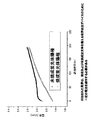
実施例1
図1は、同一の真空チャンバにおける、電界放出デバイスの2つの異なるサンプルの同時の試験からの、一定の放出電流を維持するために必要とされた印加された電界を示す。黒四角の曲線は未焼成の蛍光体層を有するサンプルに対応し、一方で、白丸の曲線は焼成された蛍光体層を有するサンプルに対応する。焼成蛍光体層と未焼成蛍光体層との主な差は、デバイスが、バインダが揮発する典型的な焼成工程に供されていないために、未焼成蛍光体層が、バインダ材料(典型的には、ポリマー、この場合エチルセルロース)と混合されたままの蛍光体粉末を含有することである。焼成蛍光体層を有するサンプルにおいては、蛍光体層は、上述の揮発効果のために残存バインダを含有しない。
Example 1
FIG. 1 shows the applied electric field required to maintain a constant emission current from the simultaneous testing of two different samples of a field emission device in the same vacuum chamber. The black square curve corresponds to the sample with the unfired phosphor layer, while the white circle curve corresponds to the sample with the fired phosphor layer. The main difference between the fired phosphor layer and the unfired phosphor layer is that the device has not been subjected to a typical firing process in which the binder is volatilized, so that the unfired phosphor layer is Is to contain the phosphor powder as mixed with the polymer, in this case ethylcellulose. In a sample having a fired phosphor layer, the phosphor layer does not contain a residual binder due to the volatilization effect described above.
初期において、未焼成蛍光体層を有するサンプルの分解速度(すなわち、現在の放出電流を維持するために必要な印加電圧の増加速度)は、焼成蛍光体層を有するサンプルのものより低い。この分解速度の差は、未焼成蛍光体層に含有される残存バインダの存在によるものである。しかしながら、使用の最中には、バインダが揮発し、分解速度は増加し始めて、焼成蛍光体層が実施の最初からバインダを含んでいなかったデバイスの速度に一致する。この実施例においては、蛍光体層を焼成する工程を省略することにより残存バインダ材料を蛍光体層中に残す技術によって、蛍光体層中の蛍光体粉末との混和物に対する保護材料の追加が提供されている。 Initially, the degradation rate of the sample with the unfired phosphor layer (ie, the rate of increase of the applied voltage required to maintain the current emission current) is lower than that of the sample with the fired phosphor layer. This difference in decomposition rate is due to the presence of residual binder contained in the unsintered phosphor layer. However, during use, the binder volatilizes and the degradation rate begins to increase, consistent with the speed of the device where the fired phosphor layer did not contain the binder from the beginning of the implementation. In this embodiment, the technique of leaving the remaining binder material in the phosphor layer by omitting the step of firing the phosphor layer provides the addition of a protective material to the admixture with the phosphor powder in the phosphor layer. Has been.
実施例2
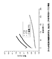
保護材料としての炭素を、ITO(インジウム錫酸化物、透明導電性材料)から構成した陽極上にスパッタ堆積した。炭素被膜は22nm厚でありおよび無定形特性であった。この炭素被覆陽極を電界放出デバイスに設置し、このデバイスにおけるエミッタの分解速度を、陽極を如何なる被膜も有さないITOから構成したデバイスと比較した。図2に示されるとおり、被覆陽極を有するデバイスにおいて、分解速度は未被覆陽極を有するデバイスに対するものよりもかなり低かった。しかしながら、約75時間後、分解速度は増加し始めたが、この増加は炭素層の消費によるものであり、これは、陽極を光学顕微鏡で検鏡した場合に物理的に観察可能であった。ITOのみの陽極の、50〜70時間での下方の曲線におけるわずかな低下は、陽極へのDCバイアスの電圧制限によるものであった。
Example 2
Carbon as a protective material was sputter deposited on an anode composed of ITO (indium tin oxide, transparent conductive material). The carbon coating was 22 nm thick and was amorphous in nature. This carbon-coated anode was placed in a field emission device and the decomposition rate of the emitter in this device was compared to a device in which the anode was composed of ITO without any coating. As shown in FIG. 2, in the device with the coated anode, the degradation rate was significantly lower than for the device with the uncoated anode. However, after about 75 hours, the degradation rate began to increase, but this increase was due to the consumption of the carbon layer, which was physically observable when the anode was examined with an optical microscope. The slight decrease in the lower curve of the ITO only anode from 50 to 70 hours was due to the voltage limitation of the DC bias to the anode.
実施例3
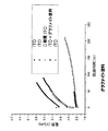
陽極上の保護炭素は、無定形である必要も、またはスパッタ堆積される必要もない。この実施例においては、グラファイトおよび無定形炭素のイソプロピルアルコール中の混合物を含有する、市販されているグラファイト塗料(Neolube No.2、Huron Industries Inc.(Port Huron,MI 48061))を用いてスピンコーティングによりITO陽極を被覆した。図3は電界放出デバイスにおけるエミッタ分解速度を示しここで、この設置した陽極は、実施例2における炭素被覆陽極を有するデバイスに対するものと類似したものであった。同時に試験した未被覆ITO陽極を有するデバイスは、実施例2における未被覆陽極を有するデバイスの性能に匹敵するかなり高い分解速度を示した。
Example 3
The protective carbon on the anode need not be amorphous or sputter deposited. In this example, a commercially available graphite paint (Neolube No. 2, Huron Industries Inc. (Port Huron, MI 48061)) containing a mixture of graphite and amorphous carbon in isopropyl alcohol was spin coated. The ITO anode was coated with FIG. 3 shows the emitter decomposition rate in a field emission device, where the installed anode was similar to that for the device with the carbon coated anode in Example 2. The device with the uncoated ITO anode tested at the same time showed a fairly high degradation rate comparable to the performance of the device with the uncoated anode in Example 2.
実施例4
電界放出ディスプレイデバイスにおいて、陽極は、度々、蛍光体で、次いでアルミニウム層で被覆されたITOガラス基板である。アルミニウム層は、陽極の前面から投じられる光量を最大化させると共に、陽極の導電性を高めるよう作用する。この構造を有する従来のデバイスは最低の分解速度のいくつかを示すことが見出された。
Example 4
In field emission display devices, the anode is often an ITO glass substrate coated with a phosphor and then with an aluminum layer. The aluminum layer acts to maximize the amount of light cast from the front surface of the anode and increase the conductivity of the anode. It has been found that conventional devices having this structure exhibit some of the lowest degradation rates.
図4は同時に試験した2つのデバイスのサンプルに対する結果を示し、黒四角での曲線は、蛍光体で被覆し、次いで焼成し、および100nmのアルミニウムを電子ビーム堆積で堆積したITO陽極を有するサンプルに対応する。白丸での曲線により表されるデバイスにおける陽極は、100nmの炭素の層をアルミニウム層の上にスパッタコートしたこと以外は同等であった。この最終炭素層は、炭素被覆陽極を有するデバイスにおけるエミッタの分解速度を劇的に低減することが見られ得る。炭素被覆陽極を有さないデバイスは電圧制限に達するまで急速に低下した一方、炭素被覆陽極を有するデバイスはより低い速度で低下した。 FIG. 4 shows the results for two device samples tested at the same time, the curve in black squares for a sample with an ITO anode coated with phosphor, then fired, and 100 nm aluminum deposited by electron beam deposition. Correspond. The anode in the device represented by the curve with open circles was equivalent except that a 100 nm carbon layer was sputter coated onto the aluminum layer. This final carbon layer can be seen to dramatically reduce the degradation rate of the emitter in a device having a carbon-coated anode. Devices without a carbon-coated anode declined rapidly until the voltage limit was reached, while devices with a carbon-coated anode declined at a slower rate.
本発明の一定の方法の特徴が、種々のこのような特徴を一緒に組み合わせる1つ以上の特定の実施形態の文脈に、本明細書において記載されている。しかしながら、本発明の範囲は、いずれかの特定の実施形態中の一定の特徴のみの記載によっては限定されず、本発明はまた、(1)記載の実施形態のいずれかの特徴のすべてより小数のサブコンビネーションであって、サブコンビネーションの形成のために省略された特徴の欠如を特徴とし得るサブコンビネーション;(2)いずれかの記載の実施形態の組み合わせ中に個別に包含される特徴の各々;ならびに(3)2つ以上の記載の実施形態の選択された特徴のみをグループ化することにより形成される特徴と、任意により、本明細書において他の箇所に開示されている他の特徴との他の組み合わせを含む。 Certain method features of the invention are described herein in the context of one or more specific embodiments that combine various such features together. However, the scope of the present invention is not limited by the description of only certain features in any particular embodiment, and the invention is also less than all of the features of any of the embodiments described in (1). A sub-combination that can be characterized by a lack of features omitted for the formation of the sub-combination; (2) each of the features individually included in the combination of any of the described embodiments; And (3) a feature formed by grouping only selected features of two or more described embodiments, and optionally other features disclosed elsewhere herein Includes other combinations.
本明細書においては、本明細書の主題の実施形態が、一定の特徴または要素を包含し、含有し、有し、これらを含んでなり、またはこれらから構成されるとして記述または説明されている用法の文脈によって、明確にそうでないと記載されていない、または反対に示されていない限りにおいて、明らかに記述または説明されているものに追加する特徴または要素の1つ以上が実施形態において存在していてもよい。本明細書の主題の代替的実施形態は、しかしながら、基本的に、一定の特徴または要素から構成されるとして記述または説明され得、この実施形態においては、作動の原理、または実施形態の特色的な特徴を実質的に変更するであろう特徴または要素はそこには存在しない。本明細書の主題のさらなる代替的実施形態は、一定の特徴または要素から構成されるとして記述または説明され得、この実施形態またはそのわずかな変形においては、特定的に記述または説明された特徴または要素のみが存在する。 As used herein, embodiments of the subject matter herein are described or described as including, containing, having, including, or consisting of certain features or elements. Depending on the context of usage, one or more of the features or elements in addition to those explicitly described or described may be present in the embodiment unless explicitly stated otherwise or indicated to the contrary. It may be. Alternative embodiments of the subject matter herein, however, may be described or described as being essentially composed of certain features or elements, in which the principles of operation or features of the embodiments are described. There are no features or elements in it that would substantially change such features. Further alternative embodiments of the subject matter herein may be described or described as being composed of certain features or elements, and in this embodiment or slight variations thereof, the features or There are only elements.
Claims (18)
Applications Claiming Priority (2)
| Application Number | Priority Date | Filing Date | Title |
|---|---|---|---|
| US90325907P | 2007-02-24 | 2007-02-24 | |
| PCT/US2008/002343 WO2008103438A1 (en) | 2007-02-24 | 2008-02-22 | Field emission device with anode coating |
Publications (2)
| Publication Number | Publication Date |
|---|---|
| JP2010519703A true JP2010519703A (en) | 2010-06-03 |
| JP2010519703A5 JP2010519703A5 (en) | 2011-04-07 |
Family
ID=39522198
Family Applications (1)
| Application Number | Title | Priority Date | Filing Date |
|---|---|---|---|
| JP2009550922A Pending JP2010519703A (en) | 2007-02-24 | 2008-02-22 | Field emission device with anode coating |
Country Status (6)
| Country | Link |
|---|---|
| US (1) | US20100072879A1 (en) |
| EP (1) | EP2126954A1 (en) |
| JP (1) | JP2010519703A (en) |
| KR (1) | KR20090113907A (en) |
| CN (1) | CN101617384A (en) |
| WO (1) | WO2008103438A1 (en) |
Families Citing this family (6)
| Publication number | Priority date | Publication date | Assignee | Title |
|---|---|---|---|---|
| KR101088106B1 (en) * | 2008-12-02 | 2011-11-30 | 한국전자통신연구원 | The field emittion display device |
| CN102810641B (en) * | 2011-05-30 | 2016-04-13 | 海洋王照明科技股份有限公司 | A kind of polymer solar battery and preparation method thereof |
| TWI492669B (en) * | 2012-08-22 | 2015-07-11 | Univ Nat Defense | Field emission anode and manufacturing method thereof |
| CN103426718B (en) * | 2013-03-25 | 2016-08-10 | 上海显恒光电科技股份有限公司 | Flat-panel radiating light source 3D print system and light source thereof |
| US10211049B2 (en) * | 2015-08-07 | 2019-02-19 | North Carolina State University | Synthesis and processing of pure and NV nanodiamonds and other nanostructures |
| JP6849224B2 (en) * | 2016-10-10 | 2021-03-24 | 京東方科技集團股▲ふん▼有限公司Boe Technology Group Co.,Ltd. | Illumination light source and its manufacturing method |
Citations (3)
| Publication number | Priority date | Publication date | Assignee | Title |
|---|---|---|---|---|
| JP2001143645A (en) * | 1999-11-11 | 2001-05-25 | Futaba Corp | Fluorescent display and its display device |
| US6353286B1 (en) * | 1999-10-08 | 2002-03-05 | Motorola, Inc | Field emission display having a multi-layered barrier structure |
| JP2005235655A (en) * | 2004-02-20 | 2005-09-02 | Hitachi Displays Ltd | Image display device |
Family Cites Families (8)
| Publication number | Priority date | Publication date | Assignee | Title |
|---|---|---|---|---|
| BE792490A (en) * | 1971-12-10 | 1973-03-30 | Gen Electric | FLUORESCENT SCREENS |
| US4857799A (en) * | 1986-07-30 | 1989-08-15 | Sri International | Matrix-addressed flat panel display |
| US5015912A (en) * | 1986-07-30 | 1991-05-14 | Sri International | Matrix-addressed flat panel display |
| ITMI991155A1 (en) * | 1999-05-25 | 2000-11-25 | Videocolor Spa | METHOD FOR METALLIZING A LUMINESCENT SCREEN |
| WO2002011169A1 (en) * | 2000-07-28 | 2002-02-07 | Candescent Technologies Corporation | Protected structure of flat panel display |
| US6645628B2 (en) * | 2001-11-13 | 2003-11-11 | The United States Of America As Represented By The Secretary Of The Air Force | Carbon nanotube coated anode |
| DE60221951T2 (en) * | 2001-11-23 | 2008-05-15 | Samsung SDI Co., Ltd., Suwon | Carbon nanotube paste composition, electron-emitting device using this composition and its production method |
| US20060255715A1 (en) * | 2004-11-09 | 2006-11-16 | Nano-Proprietary, Inc. | Carbon nanotube containing phosphor |
-
2008
- 2008-02-22 EP EP08725932A patent/EP2126954A1/en not_active Withdrawn
- 2008-02-22 JP JP2009550922A patent/JP2010519703A/en active Pending
- 2008-02-22 CN CN200880005849A patent/CN101617384A/en active Pending
- 2008-02-22 KR KR1020097019851A patent/KR20090113907A/en not_active Application Discontinuation
- 2008-02-22 US US12/525,696 patent/US20100072879A1/en not_active Abandoned
- 2008-02-22 WO PCT/US2008/002343 patent/WO2008103438A1/en active Application Filing
Patent Citations (3)
| Publication number | Priority date | Publication date | Assignee | Title |
|---|---|---|---|---|
| US6353286B1 (en) * | 1999-10-08 | 2002-03-05 | Motorola, Inc | Field emission display having a multi-layered barrier structure |
| JP2001143645A (en) * | 1999-11-11 | 2001-05-25 | Futaba Corp | Fluorescent display and its display device |
| JP2005235655A (en) * | 2004-02-20 | 2005-09-02 | Hitachi Displays Ltd | Image display device |
Also Published As
| Publication number | Publication date |
|---|---|
| WO2008103438A1 (en) | 2008-08-28 |
| CN101617384A (en) | 2009-12-30 |
| EP2126954A1 (en) | 2009-12-02 |
| KR20090113907A (en) | 2009-11-02 |
| US20100072879A1 (en) | 2010-03-25 |
Similar Documents
| Publication | Publication Date | Title |
|---|---|---|
| US7736209B2 (en) | Enhanced electron field emission from carbon nanotubes without activation | |
| Jin et al. | Enhanced electron emission from functionalized carbon nanotubes with a barium strontium oxide coating produced by magnetron sputtering | |
| US20060269750A1 (en) | Phosphor for low-voltage electron beam, method of producing the same, and vacuum fluorescent display | |
| US20060226763A1 (en) | Display device with electron emitters and method for making the same | |
| US20030222560A1 (en) | Catalytically grown carbon fiber field emitters and field emitter cathodes made therefrom | |
| JP2010519703A (en) | Field emission device with anode coating | |
| JP2006120636A (en) | Composition for forming electron emission source, method for manufacturing electron emission source using the same, and electron emission source | |
| WO2003085688A1 (en) | Field electron emission film, field electron emission electrode and field electron emission display | |
| JP2003203557A (en) | Complex for paste including carbon nanotube and electron emitting element using this complex and method of manufacture | |
| KR100550485B1 (en) | Ion-Bombarded Graphite Electron Emitters | |
| EP1285450A1 (en) | Catalytically grown carbon fiber field emitters and field emitter cathodes made therefrom | |
| JP2005524198A (en) | Electron field emitter and related compositions | |
| US20100133983A1 (en) | Method for manufacturing a field emitter electrode using the array of nanowires | |
| Shimoi et al. | A stand-alone flat-plane lighting device in a diode structure employing highly crystalline SWCNTs as field emitters | |
| KR20010033106A (en) | Ion Bombarded Graphite Electron Emitters | |
| Shimoi et al. | Field-emission durability employing highly crystalline single-walled carbon nanotubes in a low vacuum with activated gas | |
| US6514112B1 (en) | Coated-wire ion bombarded graphite electron emitters | |
| JP5549028B2 (en) | Method for producing flaky nanocarbon material, electron-emitting device, and surface-emitting device | |
| JP2007149616A (en) | Field emission element and its manufacturing method | |
| CN102124535A (en) | Method of making air-fired cathode assemblies in field emission devices | |
| JP5549027B2 (en) | Method for producing particulate nanocarbon material, electron-emitting device, and surface-emitting device | |
| JP2007280949A (en) | Field emission electrode using carbon nanotube and its manufacturing method | |
| JP4984130B2 (en) | Nanocarbon emitter, manufacturing method thereof, and surface light emitting device | |
| CN102479649A (en) | Field emitter cathode of carbon fiber material | |
| JP2008053177A (en) | Nano carbon emitter, its manufacturing method and surface light emitting device |
Legal Events
| Date | Code | Title | Description |
|---|---|---|---|
| A521 | Written amendment |
Free format text: JAPANESE INTERMEDIATE CODE: A523 Effective date: 20110216 |
|
| A621 | Written request for application examination |
Free format text: JAPANESE INTERMEDIATE CODE: A621 Effective date: 20110216 |
|
| A977 | Report on retrieval |
Free format text: JAPANESE INTERMEDIATE CODE: A971007 Effective date: 20120116 |
|
| A131 | Notification of reasons for refusal |
Free format text: JAPANESE INTERMEDIATE CODE: A131 Effective date: 20120124 |
|
| A521 | Written amendment |
Free format text: JAPANESE INTERMEDIATE CODE: A523 Effective date: 20120412 |
|
| A02 | Decision of refusal |
Free format text: JAPANESE INTERMEDIATE CODE: A02 Effective date: 20120612 |