JP2010511368A - Circuit to clamp current in charge pump - Google Patents
Circuit to clamp current in charge pump Download PDFInfo
- Publication number
- JP2010511368A JP2010511368A JP2009538559A JP2009538559A JP2010511368A JP 2010511368 A JP2010511368 A JP 2010511368A JP 2009538559 A JP2009538559 A JP 2009538559A JP 2009538559 A JP2009538559 A JP 2009538559A JP 2010511368 A JP2010511368 A JP 2010511368A
- Authority
- JP
- Japan
- Prior art keywords
- transistor
- current
- transistors
- node
- path
- Prior art date
- Legal status (The legal status is an assumption and is not a legal conclusion. Google has not performed a legal analysis and makes no representation as to the accuracy of the status listed.)
- Granted
Links
- 239000003990 capacitor Substances 0.000 claims abstract description 61
- 230000003071 parasitic effect Effects 0.000 claims description 50
- 230000005540 biological transmission Effects 0.000 claims description 34
- 238000000034 method Methods 0.000 claims description 22
- 230000007704 transition Effects 0.000 claims description 11
- 230000003111 delayed effect Effects 0.000 claims description 4
- 238000010586 diagram Methods 0.000 description 36
- 230000003068 static effect Effects 0.000 description 8
- 230000000694 effects Effects 0.000 description 6
- 230000007423 decrease Effects 0.000 description 4
- 230000006870 function Effects 0.000 description 3
- 230000008878 coupling Effects 0.000 description 2
- 238000010168 coupling process Methods 0.000 description 2
- 238000005859 coupling reaction Methods 0.000 description 2
- 238000002347 injection Methods 0.000 description 2
- 239000007924 injection Substances 0.000 description 2
- 230000033228 biological regulation Effects 0.000 description 1
- 230000008859 change Effects 0.000 description 1
- 230000001934 delay Effects 0.000 description 1
- 238000012986 modification Methods 0.000 description 1
- 230000004048 modification Effects 0.000 description 1
- 230000008569 process Effects 0.000 description 1
- 238000004088 simulation Methods 0.000 description 1
Images
Classifications
-
- H—ELECTRICITY
- H02—GENERATION; CONVERSION OR DISTRIBUTION OF ELECTRIC POWER
- H02M—APPARATUS FOR CONVERSION BETWEEN AC AND AC, BETWEEN AC AND DC, OR BETWEEN DC AND DC, AND FOR USE WITH MAINS OR SIMILAR POWER SUPPLY SYSTEMS; CONVERSION OF DC OR AC INPUT POWER INTO SURGE OUTPUT POWER; CONTROL OR REGULATION THEREOF
- H02M3/00—Conversion of dc power input into dc power output
- H02M3/02—Conversion of dc power input into dc power output without intermediate conversion into ac
- H02M3/04—Conversion of dc power input into dc power output without intermediate conversion into ac by static converters
- H02M3/06—Conversion of dc power input into dc power output without intermediate conversion into ac by static converters using resistors or capacitors, e.g. potential divider
- H02M3/07—Conversion of dc power input into dc power output without intermediate conversion into ac by static converters using resistors or capacitors, e.g. potential divider using capacitors charged and discharged alternately by semiconductor devices with control electrode, e.g. charge pumps
-
- G—PHYSICS
- G05—CONTROLLING; REGULATING
- G05F—SYSTEMS FOR REGULATING ELECTRIC OR MAGNETIC VARIABLES
- G05F1/00—Automatic systems in which deviations of an electric quantity from one or more predetermined values are detected at the output of the system and fed back to a device within the system to restore the detected quantity to its predetermined value or values, i.e. retroactive systems
- G05F1/10—Regulating voltage or current
- G05F1/625—Regulating voltage or current wherein it is irrelevant whether the variable actually regulated is ac or dc
-
- G—PHYSICS
- G05—CONTROLLING; REGULATING
- G05F—SYSTEMS FOR REGULATING ELECTRIC OR MAGNETIC VARIABLES
- G05F3/00—Non-retroactive systems for regulating electric variables by using an uncontrolled element, or an uncontrolled combination of elements, such element or such combination having self-regulating properties
- G05F3/02—Regulating voltage or current
-
- H—ELECTRICITY
- H02—GENERATION; CONVERSION OR DISTRIBUTION OF ELECTRIC POWER
- H02M—APPARATUS FOR CONVERSION BETWEEN AC AND AC, BETWEEN AC AND DC, OR BETWEEN DC AND DC, AND FOR USE WITH MAINS OR SIMILAR POWER SUPPLY SYSTEMS; CONVERSION OF DC OR AC INPUT POWER INTO SURGE OUTPUT POWER; CONTROL OR REGULATION THEREOF
- H02M1/00—Details of apparatus for conversion
- H02M1/32—Means for protecting converters other than automatic disconnection
- H02M1/34—Snubber circuits
-
- H—ELECTRICITY
- H02—GENERATION; CONVERSION OR DISTRIBUTION OF ELECTRIC POWER
- H02M—APPARATUS FOR CONVERSION BETWEEN AC AND AC, BETWEEN AC AND DC, OR BETWEEN DC AND DC, AND FOR USE WITH MAINS OR SIMILAR POWER SUPPLY SYSTEMS; CONVERSION OF DC OR AC INPUT POWER INTO SURGE OUTPUT POWER; CONTROL OR REGULATION THEREOF
- H02M3/00—Conversion of dc power input into dc power output
- H02M3/02—Conversion of dc power input into dc power output without intermediate conversion into ac
- H02M3/04—Conversion of dc power input into dc power output without intermediate conversion into ac by static converters
- H02M3/06—Conversion of dc power input into dc power output without intermediate conversion into ac by static converters using resistors or capacitors, e.g. potential divider
- H02M3/07—Conversion of dc power input into dc power output without intermediate conversion into ac by static converters using resistors or capacitors, e.g. potential divider using capacitors charged and discharged alternately by semiconductor devices with control electrode, e.g. charge pumps
- H02M3/073—Charge pumps of the Schenkel-type
-
- H—ELECTRICITY
- H03—ELECTRONIC CIRCUITRY
- H03K—PULSE TECHNIQUE
- H03K5/00—Manipulating of pulses not covered by one of the other main groups of this subclass
- H03K5/01—Shaping pulses
- H03K5/08—Shaping pulses by limiting; by thresholding; by slicing, i.e. combined limiting and thresholding
- H03K5/082—Shaping pulses by limiting; by thresholding; by slicing, i.e. combined limiting and thresholding with an adaptive threshold
- H03K5/086—Shaping pulses by limiting; by thresholding; by slicing, i.e. combined limiting and thresholding with an adaptive threshold generated by feedback
-
- H—ELECTRICITY
- H03—ELECTRONIC CIRCUITRY
- H03K—PULSE TECHNIQUE
- H03K5/00—Manipulating of pulses not covered by one of the other main groups of this subclass
- H03K5/13—Arrangements having a single output and transforming input signals into pulses delivered at desired time intervals
-
- H—ELECTRICITY
- H03—ELECTRONIC CIRCUITRY
- H03L—AUTOMATIC CONTROL, STARTING, SYNCHRONISATION OR STABILISATION OF GENERATORS OF ELECTRONIC OSCILLATIONS OR PULSES
- H03L7/00—Automatic control of frequency or phase; Synchronisation
- H03L7/06—Automatic control of frequency or phase; Synchronisation using a reference signal applied to a frequency- or phase-locked loop
- H03L7/08—Details of the phase-locked loop
- H03L7/085—Details of the phase-locked loop concerning mainly the frequency- or phase-detection arrangement including the filtering or amplification of its output signal
- H03L7/089—Details of the phase-locked loop concerning mainly the frequency- or phase-detection arrangement including the filtering or amplification of its output signal the phase or frequency detector generating up-down pulses
- H03L7/0891—Details of the phase-locked loop concerning mainly the frequency- or phase-detection arrangement including the filtering or amplification of its output signal the phase or frequency detector generating up-down pulses the up-down pulses controlling source and sink current generators, e.g. a charge pump
- H03L7/0895—Details of the current generators
-
- H—ELECTRICITY
- H03—ELECTRONIC CIRCUITRY
- H03L—AUTOMATIC CONTROL, STARTING, SYNCHRONISATION OR STABILISATION OF GENERATORS OF ELECTRONIC OSCILLATIONS OR PULSES
- H03L7/00—Automatic control of frequency or phase; Synchronisation
- H03L7/06—Automatic control of frequency or phase; Synchronisation using a reference signal applied to a frequency- or phase-locked loop
- H03L7/08—Details of the phase-locked loop
- H03L7/099—Details of the phase-locked loop concerning mainly the controlled oscillator of the loop
Landscapes
- Engineering & Computer Science (AREA)
- Power Engineering (AREA)
- Physics & Mathematics (AREA)
- Electromagnetism (AREA)
- General Physics & Mathematics (AREA)
- Radar, Positioning & Navigation (AREA)
- Automation & Control Theory (AREA)
- Nonlinear Science (AREA)
- Stabilization Of Oscillater, Synchronisation, Frequency Synthesizers (AREA)
- Dc-Dc Converters (AREA)
- Electronic Switches (AREA)
- Semiconductor Integrated Circuits (AREA)
Abstract
チャージポンプにおいて電流をクランプする回路が開示される。チャージポンプは、複数のスイッチング回路トランジスタを有するスイッチング回路を備える。同回路における第1及び第2の対のトランジスタの各々は、スイッチング回路トランジスタの内の対応する1つからの電流に対して、電流におけるスパイクが、同スイッチング回路トランジスタとチャージポンプのキャパシタとの間を通る経路を通って部分的にだけ伝送されるように、そのトランジスタがオフに切り替わっている間に追加経路を提供することができる。A circuit for clamping current in a charge pump is disclosed. The charge pump includes a switching circuit having a plurality of switching circuit transistors. Each of the first and second pairs of transistors in the circuit has a current spike between the switching circuit transistor and the charge pump capacitor relative to the current from a corresponding one of the switching circuit transistors. An additional path can be provided while the transistor is switched off so that it is only partially transmitted through the path through.
Description
当業者に理解されるように、チャージポンプは、より高いまたはより低い電圧のいずれかを作り出すためにキャパシタを用いる回路として特徴付けることができる。チャージポンプは、例えば遅延ロックループ(DLL)及びフェーズロックループ(PLL)を伴う用途等、多種多様な用途に用いられる。 As will be appreciated by those skilled in the art, charge pumps can be characterized as circuits that use capacitors to create either higher or lower voltages. Charge pumps are used in a wide variety of applications, such as applications involving delay locked loops (DLLs) and phase locked loops (PLLs).
PLLに関して、チャージポンプは、電圧制御発振器(VCO)に印加される制御電圧を供給するために用いることができる。通常、PLLは、位相検出器と、チャージポンプの出力に連結されたループフィルタと、増幅器と、フィードバック系を形成するように公知の方法で相互接続されたVCOとを備える。チャージポンプは、位相検出器によって生成される論理レベルパルスを、ループフィルタに供給される電流パルスに変換する。ループフィルタは、VCO用の制御電圧を生成するために電流パルスを積分する。 With respect to the PLL, the charge pump can be used to provide a control voltage that is applied to a voltage controlled oscillator (VCO). The PLL typically comprises a phase detector, a loop filter coupled to the output of the charge pump, an amplifier, and a VCO interconnected in a known manner to form a feedback system. The charge pump converts the logic level pulses generated by the phase detector into current pulses that are supplied to the loop filter. The loop filter integrates the current pulse to generate a control voltage for the VCO.
DLLに関して、チャージポンプは、DLLの電圧制御遅延線(VCDL)に制御電圧を供給するために用いることができる。当業者に理解されるように、特定種類の装置(例えば、DRAM装置)では、DLLはクロック信号の位相を変化させるために用いることができる。この場合、DLLは直列(デイジー・チェイン状)に接続された複数の遅延ゲートからなる遅延チェーンを備える。 For a DLL, the charge pump can be used to supply a control voltage to the DLL's voltage controlled delay line (VCDL). As will be appreciated by those skilled in the art, in certain types of devices (eg, DRAM devices), the DLL can be used to change the phase of the clock signal. In this case, the DLL includes a delay chain composed of a plurality of delay gates connected in series (daisy chained).
DLL及びPLLを伴う用途以外にも、例えば、チャージポンプを、フィルタまたは貯留キャパシタに対して電圧調整を行うための正確に制御された(accurately−controlled)電流源/シンクを有する電子回路において用いるといった他の用途があることを当業者は理解するだろう。 In addition to applications involving DLLs and PLLs, for example, charge pumps are used in electronic circuits with accurately-controlled current sources / sinks for voltage regulation on filters or storage capacitors. One skilled in the art will appreciate that there are other uses.
一実施形態によれば、チャージポンプにおいて電流をクランプする方法が開示される。チャージポンプは、スイッチング回路とキャパシタとを備える。チャージポンプは第1及び第2の経路を形成する。第1及び第2の経路のそれぞれについて、選択された方を通って(i)電流が前記キャパシタに電流を供給され、(ii)電流が前記キャパシタから供給される。前記スイッチング回路の複数のトランジスタの少なくとも1つからの電流内に、少なくとも一つの寄生スパイクがその少なくとも1つのトランジスタがオフに切り替わっている間に生成される。短い期間が経過した後、前記少なくとも1つの寄生スパイクは消滅する。本発明の方法は、その値が第1の値から第2の値に変化した時に前記少なくとも1つのトランジスタをオフに切り替わらせる制御信号を少なくとも1つ供給する工程を含む。同方法は、前記少なくとも1つの寄生スパイクが、前記第1及び第2の経路の内の選択された一方を通って部分的にだけ伝達されるように、前記少なくとも1つの制御信号の値が第1の値から第2の値に変化した時に、前記少なくとも1つのトランジスタからの電流に対する追加経路を形成する工程も含む。同方法は、前記追加経路が前記短い期間の間形成された後に、前記追加経路を解消させる工程も含む。 According to one embodiment, a method for clamping current in a charge pump is disclosed. The charge pump includes a switching circuit and a capacitor. The charge pump forms first and second paths. For each of the first and second paths, through a selected one, (i) current is supplied to the capacitor and (ii) current is supplied from the capacitor. In the current from at least one of the plurality of transistors of the switching circuit, at least one parasitic spike is generated while the at least one transistor is switched off. After a short period of time, the at least one parasitic spike disappears. The method of the present invention includes providing at least one control signal that switches the at least one transistor off when its value changes from a first value to a second value. The method is characterized in that the value of the at least one control signal is such that the at least one parasitic spike is only partially transmitted through a selected one of the first and second paths. Forming an additional path for current from the at least one transistor when changing from a value of 1 to a second value. The method also includes the step of eliminating the additional path after the additional path is formed for the short period of time.
別の実施形態によれば、チャージポンプにおいて電流をクランプする回路が開示される。前記チャージポンプは、スイッチング回路とキャパシタとを備え、前記チャージポンプは第1及び第2の経路を形成する。第1及び第2の経路のそれぞれについて、選択された方を通ってi)電流が前記キャパシタに供給され、ii)電流が前記キャパシタから供給される。前記スイッチング回路の複数のトランジスタの内の少なくとも1つからの電流内に、少なくとも1つの寄生スパイクが、その少なくとも1つのトランジスタがオフに切り替わっている間に生成される。本発明の回路は、第1及び第2の対のトランジスタを備え、同トランジスタの各々はオン及びオフ状態をサポートし、前記状態間の遷移を制御できるように制御電極を備える。前記第1の対のトランジスタの内の一方は、第1のノードを介して前記スイッチング回路のトランジスタの内の最初のトランジスタに電気的に接続されている。前記第1の経路は前記第1のノードを通って伸びている。前記第2の対のトランジスタの内の一方は、第2のノードを介して前記スイッチング回路のトランジスタの内の二番目のトランジスタに電気的に接続されている。前記第2の経路は前記第2のノードを通って伸びている。本発明の回路はまた、第1の遅延導入インバータ回路と、第2の遅延導入インバータ回路とを備え、前記第1のインバータ回路及び前記第2のインバータ回路の各々は、前記それぞれの対のトランジスタの内の一方の制御電極に入力される信号を入力信号とし、前記それぞれの対のトランジスタの内の他方の制御電極に遅延出力信号を供給する。前記オフへの切り替えが起こる瞬間、前記入力信号と前記遅延出力信号の双方は、前記オン状態を作り出す値を有する。前記第1及び第2の対のトランジスタの内の少なくとも一方は、前記少なくとも1つの寄生スパイクが、前記キャパシタに向かういずれかの経路を通って部分的にだけ伝達されるように、前記オフに切り替わっている間、前記トランジスタの内の前記少なくとも1つからの電流に対する追加経路を形成する。 According to another embodiment, a circuit for clamping current in a charge pump is disclosed. The charge pump includes a switching circuit and a capacitor, and the charge pump forms first and second paths. For each of the first and second paths, i) current is supplied to the capacitor through the selected one, and ii) current is supplied from the capacitor. In a current from at least one of the plurality of transistors of the switching circuit, at least one parasitic spike is generated while the at least one transistor is switched off. The circuit of the present invention comprises a first and a second pair of transistors, each of which comprises a control electrode to support on and off states and to control transitions between the states. One of the first pair of transistors is electrically connected to the first transistor of the transistors of the switching circuit through a first node. The first path extends through the first node. One of the second pair of transistors is electrically connected to a second transistor of the transistors of the switching circuit through a second node. The second path extends through the second node. The circuit of the present invention also includes a first delay introducing inverter circuit and a second delay introducing inverter circuit, wherein each of the first inverter circuit and the second inverter circuit includes the respective pair of transistors. A signal input to one of the control electrodes is used as an input signal, and a delayed output signal is supplied to the other control electrode of the pair of transistors. At the instant when the switch-off occurs, both the input signal and the delayed output signal have values that create the on-state. At least one of the first and second pairs of transistors switches off such that the at least one parasitic spike is only partially transmitted through any path toward the capacitor. During this time, an additional path for current from the at least one of the transistors is formed.
別の実施形態によれば、チャージポンプを備える装置が開示される。前記チャージポンプは複数のスイッチングトランジスタと、電流クランプ回路と、キャパシタとを備える。前記チャージポンプは、第1及び第2の経路を形成する。第1及び第2の経路のそれぞれについて、選択された方を通ってi)電流が前記キャパシタに供給され、ii)電流が前記キャパシタから供給される。前記スイッチングトランジスタの内の1つは、前記第1及び第2の経路の内の選択された一方に位置している。そのスイッチングトランジスタは、オフに切り替わった時に、電流内に寄生スパイクを生成する。その寄生スパイクは、短い期間が経過した後で消滅する。その値が第1の値から第2の値に変化した時に、前記スイッチングトランジスタをオフに切り替わらせる制御信号を供給する入力を有する。前記電流クランプ回路は、(i)前記少なくとも1つの寄生スパイクが、前記第1及び第2の経路の内の前記一方を通って部分的にだけ伝達されるように、前記制御信号の値が前記第1の値から前記第2の値に変化した時に、前記スイッチングトランジスタからの電流に対する追加経路を形成し、(ii)前記追加経路が前記短い期間の間形成された後に、前記追加経路を解消させる。 According to another embodiment, an apparatus comprising a charge pump is disclosed. The charge pump includes a plurality of switching transistors, a current clamp circuit, and a capacitor. The charge pump forms first and second paths. For each of the first and second paths, i) current is supplied to the capacitor through the selected one, and ii) current is supplied from the capacitor. One of the switching transistors is located on a selected one of the first and second paths. The switching transistor generates a parasitic spike in the current when switched off. The parasitic spikes disappear after a short period of time. When the value changes from the first value to the second value, it has an input for supplying a control signal for switching the switching transistor off. The current clamp circuit has (i) the value of the control signal is such that the at least one parasitic spike is only partially transmitted through the one of the first and second paths. Forming an additional path for the current from the switching transistor when changing from a first value to the second value; (ii) eliminating the additional path after the additional path is formed for the short period of time Let
別の実施形態によれば、チャージポンプにおいて電流をクランプする方法が開示される。前記チャージポンプは複数のスイッチングトランジスタと、電流クランプ回路と、キャパシタとを備える。前記チャージポンプは、第1及び第2の経路を形成する。第1及び第2の経路のそれぞれについて、選択された方を通ってi)電流が前記キャパシタに供給され、ii)電流が前記キャパシタから供給される。前記スイッチング回路の複数のトランジスタの内の少なくとも1つからの電流内に、少なくとも1つの寄生スパイクがその少なくとも1つのトランジスタがオフに切り替わっている間に生成される。本発明の方法は、その値が第1の値から第2の値に変化した時に、前記少なくとも1つのトランジスタをオフに切り替わらせる制御信号を少なくとも1つ供給する工程を含む。本発明の方法は、前記少なくとも1つの寄生スパイクが、前記第1及び第2の経路の内の選択された一方を通って部分的にだけ伝達されるように、前記少なくとも1つの制御信号の値が前記第1の値から前記第2の値に変化した時に、前記トランジスタの内の前記少なくとも1つからの電流に対する追加経路を形成する工程も含む。前記追加経路は第1のノードを介して前記トランジスタの内の前記少なくとも1つに提供される。前記少なくとも1つのトランジスタがオフに切り替わっている間に前記第1のノードにおける電圧の値は変化する。本発明の方法は、前記トランジスタの内の前記少なくとも1つがオフに切り替わった後に、前記第1及び第2の経路の内の前記一方上のトランジスタを流れる漏れ電流を、前記キャパシタを基準として最小限にする工程も含む。 According to another embodiment, a method for clamping current in a charge pump is disclosed. The charge pump includes a plurality of switching transistors, a current clamp circuit, and a capacitor. The charge pump forms first and second paths. For each of the first and second paths, i) current is supplied to the capacitor through the selected one, and ii) current is supplied from the capacitor. At least one parasitic spike is generated in the current from at least one of the plurality of transistors of the switching circuit while the at least one transistor is switched off. The method of the present invention includes providing at least one control signal that switches the at least one transistor off when the value changes from a first value to a second value. The method of the present invention provides for the value of the at least one control signal such that the at least one parasitic spike is only partially transmitted through a selected one of the first and second paths. Forming an additional path for current from the at least one of the transistors when the value changes from the first value to the second value. The additional path is provided to the at least one of the transistors via a first node. The value of the voltage at the first node changes while the at least one transistor is switched off. The method of the present invention minimizes leakage current flowing through the transistor on one of the first and second paths after the at least one of the transistors is switched off with respect to the capacitor. The process of making is also included.
前記漏れ電流の流れを最小限にする工程は、前記少なくとも1つのトランジスタがオフに切り替わっている間に、前記第1のノードにおける電圧が固定電圧値から遠ざかるのを防ぐことを含むことが好ましい。 Preferably, the step of minimizing leakage current flow includes preventing the voltage at the first node from moving away from a fixed voltage value while the at least one transistor is switched off.
本発明の方法は、前記追加経路が形成された後に、同経路を瞬時に解消させる工程をさらに含むことが好ましい。 The method of the present invention preferably further includes a step of instantaneously canceling the additional path after the additional path is formed.
別の実施形態によれば、チャージポンプを備えた装置が提供される。前記チャージポンプは複数のスイッチングトランジスタと、電流クランプ回路と、キャパシタとを備え、前記チャージポンプは、第1及び第2の経路を形成する。第1及び第2の経路のそれぞれについて、選択された方を通ってi)電流が前記キャパシタに供給され、ii)電流が前記キャパシタから供給される。前記スイッチングトランジスタの内の1つは、前記第1及び第2の経路の内の選択された一方に位置している。そのスイッチングトランジスタは、オフに切り替わった時に、電流内に寄生スパイクを生成する。回路は、その値が第1の値から第2の値に変化した時に前記スイッチングトランジスタをオフに切り替わらせる制御信号を供給することができる。前記電流クランプ回路は、(i)前記寄生スパイクが、前記第1及び第2の経路の内の前記一方を通って部分的にだけ伝達されるように、前記制御信号の値が前記第一の値から前記第2の値に変化した時に、前記スイッチングトランジスタからの電流に対する追加経路を形成する。前記追加経路は、前記第1のノードを介して前記スイッチングトランジスタに提供される。前記スイッチングトランジスタがオフに切り替わっている間、前記第1のノードにおける電圧の値は変化する。前記電流クランプ回路はまた(ii)前記トランジスタの内の前記少なくとも1つのトランジスタがオフに切り替わった後に、前記第1及び第2の経路の内の前記一方上のトランジスタを流れる漏れ電流を、前記キャパシタを基準として最小限にする。 According to another embodiment, an apparatus with a charge pump is provided. The charge pump includes a plurality of switching transistors, a current clamp circuit, and a capacitor, and the charge pump forms first and second paths. For each of the first and second paths, i) current is supplied to the capacitor through the selected one, and ii) current is supplied from the capacitor. One of the switching transistors is located on a selected one of the first and second paths. The switching transistor generates a parasitic spike in the current when switched off. The circuit can provide a control signal that switches the switching transistor off when its value changes from a first value to a second value. The current clamp circuit may: (i) the value of the control signal is the first value so that the parasitic spike is only partially transmitted through the one of the first and second paths. When changing from a value to the second value, an additional path for the current from the switching transistor is formed. The additional path is provided to the switching transistor via the first node. While the switching transistor is switched off, the value of the voltage at the first node changes. The current clamp circuit also (ii) detects a leakage current flowing through the transistor on the one of the first and second paths after the at least one of the transistors is switched off. To the minimum.
前記漏れ電流の流れを最小限にすることは、前記少なくとも1つのトランジスタがオフに切り替わっている間、前記第1のノードにおける電圧が固定電圧値から遠ざかるのを防ぐことを含むことが好ましい。 Minimizing the leakage current flow preferably includes preventing the voltage at the first node from moving away from a fixed voltage value while the at least one transistor is switched off.
前記チャージポンプはさらに、双方が前記キャパシタに電気的に接続された第1及び第2のFETを備え、第1のFETは前記第1の経路に沿って配置され、第2のFETは前記第2の経路に沿って配置されていることが好ましい。 The charge pump further includes first and second FETs, both electrically connected to the capacitor, the first FET being disposed along the first path, and the second FET being the first FET. It is preferable to arrange | position along 2 path | routes.
前記電流クランプ回路は、直列に接続され前記追加経路に沿って設置された2つのトランジスタを備え、前記電流クランプ回路は、前記追加経路が形成されると、前記第1のノードを、前記2つのトランジスタの間の第2のノードに連結することが好ましい。 The current clamp circuit includes two transistors connected in series and disposed along the additional path. The current clamp circuit, when the additional path is formed, causes the first node to pass through the two nodes. It is preferably connected to a second node between the transistors.
前記チャージポンプはさらに、前記キャパシタにおけるVcノードを形成し、前記電流クランプ回路は、前記Vcノードにおける電圧の複製を生成する中継器を備え、その複製された電圧は、前記追加経路が一旦形成されると前記第1のノードに連結されることが好ましい。 The charge pump further forms a V c node in the capacitor, and the current clamp circuit includes a repeater that generates a replica of the voltage at the V c node, the replicated voltage once the additional path is Once formed, it is preferably connected to the first node.
従って、チャージポンプ内の電流をクランプする回路を向上させるのに有利であろう。 Therefore, it would be advantageous to improve the circuit that clamps the current in the charge pump.
以下の実施形態の詳細な説明では、図示される回路及び回路部品の多くは、電子信号に対して公知の動作を行う種類のものである。当業者は、それらと同等と認識される代替の回路または回路部品についての知識を有するであろう。何故なら、それらは同信号に対して同じ動作を行うからである。 In the detailed description of the embodiments below, many of the illustrated circuits and circuit components are of the type that perform known operations on electronic signals. Those skilled in the art will have knowledge of alternative circuits or circuit components that are recognized as being equivalent thereto. Because they perform the same operation on the same signal.
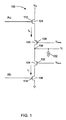
図面を参照して、図1はチャージポンプ100の模式回路図である。いくつかの例では、チャージポンプ100はメモリ回路(例えばDRAM)の一部であり、VCOに印加される電圧を制御するためにPLLにおいて用いられる。他の例では、チャージポンプ100は同様に、ある種のメモリ回路の一部であってもよく、PLLではなく、例えばDLLにおいて用いられる。さらに別の例では、チャージポンプ100はクロック管理/配信回路、メモリインターフェイス、FPGAモジュール等の一部であってもよい。
Referring to the drawings, FIG. 1 is a schematic circuit diagram of a
チャージポンプ100はキャパシタ102を備える。チャージポンプ100はスイッチング回路も備え、本実施形態においてそれはPMOSスイッチング・トランジスタ104とNMOSスイッチング・トランジスタ108からなる。スイッチング・トランジスタ104は、同トランジスタのゲート112に印加されるポンプアップ制御信号PUに応じて切り替わる。スイッチング・トランジスタ108は、同トランジスタのゲート116に印加されるポンプダウン制御信号PDに応じて切り替わる。
The
図示したチャージポンプ100に関して、スイッチング・トランジスタ104またはスイッチング・トランジスタ108のいずれも出力ノードVcに直接には接続されていない。当業者は、スイッチング・トランジスタが出力ノードに直接接続された回路についての知識を有しているだろうが、そのような構成の欠点の一つは、スイッチング・トランジスタのゲートで信号遷移がある場合、出力ノードに寄生ノイズが導入されてしまうという点である。
Regard the
本実施形態において、それぞれ、ゲートにバイアス電圧が印加されたPMOSトランジスタ120とNMOSトランジスタ124が、2つのスイッチング・トランジスタ104と108との間に接続されている。いくつかの例では、バイアス電圧を供給する電圧基準ソースを実現するために電流ミラーが用いられる。ゲート128にVbiaspが印加されたトランジスタ120は、電流Ipが同トランジスタのチャンネルを流れることが可能な状態であり、ゲート112に印加される信号PUの要求に従ってスイッチング・トランジスタ104がオンになった場合に、ノード130に供給される。当業者に理解されるように、ゲートはFETの制御電極であり、FETのオン状態とオフ状態との遷移を制御可能にするものである。他の種類のトランジスタでは、制御電極は必ずしもゲートという名称で呼ばれる訳ではない。例えば、バイポーラトランジスタでは、バイポーラトランジスタの制御電極を言及する際に通常用いられる用語は「ベース」である。
In the present embodiment, a
信号PUがロジック「ハイ」からロジック「ロー」に変化した時に、スイッチング・トランジスタ104がオンに切り替わることが分かる。また反対に、信号PUがロジックローからロジックハイに変化した時に、スイッチング・トランジスタ104はオフに切り替わる。それに対して、ゲート132にVbiasnが印加されたトランジスタ124は、ゲート116に印加される信号PDの要求に従ってスイッチング・トランジスタ108がオンになった場合に、電流Inがノード130から排流されるように同トランジスタのチャンネルを流れることが可能な状態にある。信号PDがロジックローからロジックハイに変化した時に、スイッチング・トランジスタ108がオンに切り替わることが分かる。また反対に、信号PDがロジックハイからロジックローに変化した時に、スイッチング・トランジスタ108はオフに切り替わる。
It can be seen that the switching
参考の便宜上、チャージポンプ100はソース部とシンク部の両方を有するものとして説明した方が正確であろう。トランジスタ112及び120はソース部の一部である。トランジスタ116及び124はシンク部の一部である(当業者は、「シンク部」は代替的に「ドレイン部」と呼ばれることを理解するだろう)。
For convenience of reference, it will be more accurate to describe the
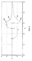
図2は電流Ip及びInの波形の一例を経時的に示す図である。図2のグラフにおいて、時間t1、t2、及びt3は、スイッチング・トランジスタ104及び108の内の1つまたはそれ以上がオンまたはオフに切り替わる場における時間に対応している。特に、時間t1の近辺でスイッチング・トランジスタ108はオンに切り替わり、時間t2の近辺でスイッチング・トランジスタ104はオンに切り替わり、時間t3の近辺でスイッチング・トランジスタ104及び108の両方はオフに切り替わる。
Figure 2 is a diagram showing an example of a waveform of the current I p and I n over time. In the graph of FIG. 2, times t 1 , t 2 , and t 3 correspond to times when one or more of the switching
時間t3を参照すれば、スイッチング・トランジスタ104がオフに切り替わる時に、電流Ipに上向きスパイク204が発生することが分かる。また、時間t3において、スイッチング・トランジスタ108がオフに切り替わる時に、電流Inには下向きスパイク208が発生する。電流スパイク204及び208は次のように説明できる。スイッチング・トランジスタ104または108のいずれかがオフに切り替わる時に、ゲート・ドレイン間容量に起因するスイッチング信号結合の結果として、それらのトランジスタは電流を生成する。この電流は、既にトランジスタを流れる電流に加算される。図1のチャージポンプにおいて、この加算された電流には近隣のトランジスタ120または124のそれぞれ以外に行き場がない。
Referring to time t 3 , it can be seen that an
当業者に理解されるように、電流スパイク204及び208はDLL/PLLのループのエラーの原因となり、それにより位相オフセットが起こる。その理由の少なくとも1つは、電流スパイク204は電流スパイク208と対称的ではないという点である。電流テイルアウト216及び220も、DLL/PLLのループのエラーの原因となり得る。当業者に理解されるように、電流テイルアウト216及び220が存在するのは、トランジスタ120及び124が急速にではなく徐々にシャットオフされる(トランジスタ120及び124のソースの電圧が急速にというよりも徐々にシャットオフ電圧値に遷移する)ためである。
As will be appreciated by those skilled in the art,
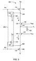
図3は、別のチャージポンプ300の概略回路図である。チャージポンプ300は、図1のチャージポンプといくつかの点では同様であるが、スイッチング・トランジスタ104または108からのオフスイッチ電流に対して経路を提供するために静的クランプ304をさらに備えている。図示した静的クランプ304は、NMOSトランジスタ308とPMOSトランジスタ312とを備える。トランジスタ308のドレイン316は、ノード320を介してスイッチング・トランジスタ104に電気的に接続されている。トランジスタ312に関し、同トランジスタのドレイン324は、ノード328を介してスイッチング・トランジスタ108に電気的に接続されている。
FIG. 3 is a schematic circuit diagram of another
チャージポンプ300の静的クランプ304は、スイッチング・トランジスタ104がオフに切り替わっている間、電流に対して追加経路を提供することで、スイッチング・トランジスタ104とキャパシタ102との間の経路に沿った電流スパイクを減少させ、また同様に、スイッチング・トランジスタ108がオフに切り替わっている間、電流に対して追加経路を同じく提供することで、スイッチング・トランジスタ108とキャパシタ102との間の経路に沿った電流スパイクを減少させる働きをする。図2に示す波形に対して静的クランプ304が持ち得る設計上の影響という意味で、図示した電流スパイク204及び208に比べ、電流スパイクの大きさは極めて小さいものになり得る。また、電流テイルアウトも低減され得る。
The
静的クランプ304をチャージポンプ300内で用いる場合の制約は、Vcが、Vbiaspにより定義される上限とVbiasnにより定義される下限との間の範囲内に制限されてしまう点である。当業者に理解されるように、このVcの制限は、スイッチング・トランジスタ104及び108がオフに切り替わった後もトランジスタ308及び312が依然としてオンのままであることに起因する。特に、ノード320における電圧は、スイッチング・トランジスタ104が一旦オフに切り替わると接地電位に達する。もしVcがVbiaspよりも大きくなると、電流は、電流Ip''を表わす矢印が示している方向とは反対の方向にトランジスタ120を流れ(Vcの電圧値が大きくなればなるほど漏れ電流が多くなる)、電流Ip''はVcの値に対し望ましくない影響を与える。同様に、ノード328における電圧は、スイッチング・トランジスタ108が一旦オフに切り替わるとVddに達する。もしVcがVbiasnより小さくなると、電流は、電流In''を表わす矢印が示している方向とは反対の方向にトランジスタ124を流れ(この場合、Vcの電圧値が小さくなればなるほど漏れ電流が多くなる)、そのため電流In''はVcの値に対して望ましくない影響を与える。
Constraint in the case of using the
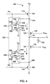
今度は図4を参照する。図4は別のチャージポンプ500の概略回路図である。チャージポンプ500は、図1のチャージポンプといくつかの点では同様であるが、一実施形態に係るクランプ504をさらに備える。静的クランプ304(図3)のように、クランプ504はスイッチング・トランジスタ104または108のいずれかからのオフスイッチ電流に対して追加経路を提供することができる。しかしながら、静的クランプ304とは異なり、クランプ504は、VbiaspとVbiasnとによって定義される限界の範囲内にVcを制限しない。
Reference is now made to FIG. FIG. 4 is a schematic circuit diagram of another
図示したクランプ504は、一対のNMOSトランジスタ508及び512と、一対のPMOSトランジスタ516及び520と、遅延導入インバータ回路(またはインバータ)524と、別の遅延導入インバータ回路528とを備える。(例えば、インバータ524及び528のそれぞれは、一対のNMOSとPMOSトランジスタといった周知のトランジスタの組み合わせを用いて実現することができる。また、図4では遅延導入インバータ回路524及び遅延導入インバータ回路528のそれぞれは1つのインバータのみとして示されているが、ある例では、遅延導入インバータ回路が1つのインバータではなく3つ以上の実際のインバータを備えることが可能であることが分かるであろう。
The illustrated
本発明の実施形態に係るクランプのインバータ回路によって導入可能な最適な遅延は、様々な要因によって変化することが分かるだろう。これらの要因には、例えば、電流に対して追加経路を提供するトランジスタの大きさや、インバータ回路を実現するために用いられるトランジスタの大きさが含まれる。 It will be appreciated that the optimum delay that can be introduced by the inverter circuit of the clamp according to embodiments of the present invention varies depending on various factors. These factors include, for example, the size of the transistor that provides an additional path for the current and the size of the transistor used to implement the inverter circuit.
図示した実施形態において、トランジスタ508と、トランジスタ512と、インバータ524とを備えるクランプ504の半分は、スイッチング・トランジスタ104と動作連動しており、トランジスタ516と、トランジスタ520と、インバータ528とを備えるクランプ504の他の半分は、スイッチング・トランジスタ108と動作連動している。
In the illustrated embodiment, half of
スイッチング・トランジスタ104と動作連動している図示したクランプ504の半分に関し、トランジスタ508のドレイン532は、ノード536を介してスイッチング・トランジスタ104に電気的に接続されている。また、トランジスタ508のソース540は、トランジスタ512のドレイン544に電気的に接続されている。インバータ524の入力548とトランジスタ508のゲート552の双方には、同じ信号、即ちPUが印加される。インバータ524の出力556は、トランジスタ512のゲート560に電気的に接続されている。
With respect to half of the illustrated
スイッチング・トランジスタ108と動作連動している図示したクランプ504の半分に関し、トランジスタ520のドレイン564は、ノード568を介してスイッチング・トランジスタ108に電気的に接続されている。また、トランジスタ520のソース572は、トランジスタ516のドレイン576に電気的に接続されている。インバータ528の入力580とトランジスタ520のゲート584の双方には、同じ信号、即ちPDが印加される。インバータ528の出力588は、トランジスタ516のゲート592に電気的に接続されている。
With respect to the half of the illustrated
スイッチング・トランジスタ104及び108がオフに同時に切り替わっている間(当然ながら、少なくともいくつかの例では、2つのトランジスタを同時にオフに切り替える必要はないことが分かるだろう)、図示したクランプ504の動作は以下の通りである。その長さがインバータ524及び528の遅延によって決定される短い期間の間、クランプ504の一部を形成する2対のトランジスタは、スイッチング・トランジスタ104及び108がオフに切り替わっている間、電流スパイクを減少させるための経路を提供する。これらの経路は、各対のトランジスタの両方がオンになることにより存在する。しかしながら、インバータの遅延によって決定される期間が経過した後、何れの対のトランジスタも、両方のトランジスタがオンではなくなるため、2対のトランジスタによるクランプ効果が解消されて、望むようにVcを設定できるという大きな柔軟性が得られる(即ち、VbiaspとVbiasnとによって定義される限界の範囲内に制限されない)。
While the switching
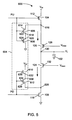
今度は図5を参照する。図5は別のチャージポンプ600の概略回路図である。チャージポンプ600は、図4のチャージポンプといくつかの点では同様であるが、別の実施形態に係るクランプ604を備える。ここで図示し説明した他のクランプのように、クランプ604は、VbiaspとVbiasnとによって定義される限界の範囲内にVcを制限しない。
Reference is now made to FIG. FIG. 5 is a schematic circuit diagram of another
図示したクランプ604は、第1の対のトランジスタ606と608と、第2の対のトランジスタ610と612とを備える。少なくとも一つの例において、トランジスタ606及び610はNMOSトランジスタであり、トランジスタ608及び612はPMOSトランジスタである。
The illustrated
図示した実施形態において、トランジスタ606及び608を備えるクランプ604の半分は、スイッチング・トランジスタ104と動作連動しており、トランジスタ610及び612を備えるクランプ604の他の半分は、スイッチング・トランジスタ108と動作連動している。
In the illustrated embodiment, half of the
スイッチング・トランジスタ104と動作連動している図示したクランプ604の半分に関し、トランジスタ606のドレイン614は、ノード616を介してスイッチング・トランジスタ104に電気的に接続されている。また、トランジスタ606のソース618は、トランジスタ608のソース620に電気的に接続されている。トランジスタ606のゲート622及びトランジスタ608のゲート624の双方には、同じ信号、即ちPUが印加される。
With respect to the half of the illustrated
スイッチング・トランジスタ108と動作連動している図示したクランプ604の半分に関し、トランジスタ612のドレイン626は、ノード628を介してスイッチング・トランジスタ108に電気的に接続されている。また、トランジスタ612のソース630は、トランジスタ610のソース632に電気的に接続されている。トランジスタ612のゲート634及びトランジスタ610のゲート636の双方には、同じ信号、即ちPDが印加される。
With respect to half of the illustrated
信号PDがロジックハイの場合、トランジスタ108及び610は導通しているのに対し、トランジスタ612は導通していない。この間、ソース639とソース632との間にあるノードは、NMOSトランジスタ610のしきい値電圧レベルと略等しい電圧レベルに事前充電される。信号PDがロジックローになると、トランジスタ610はオフになり漏れ経路をカットオフする。また、PMOSトランジスタ612はオンになり、ノード628と、ソース639とソース632との間にあるノードとの間の電荷交換を行わせる。例えば、電荷交換は、2つのトランジスタ610及び612の寄生容量の間で発生する。この電荷交換の間、寄生電流スパイクがスイッチング・トランジスタ108とキャパシタ102との間の経路を部分的にだけ通るよう、ノード628を通る追加電流経路が提供される。電荷交換の結果、ノード628の電流レベルは急速に上昇し、トランジスタ124を急速にカットオフする。このパッシブな状態の間、漏れ電流の流れを最小限にするために、ノード628における電圧が遷移する新たな電圧値は、スイッチング・トランジスタ108がオフに切り替わっている間維持される。
When signal PD is logic high,
同様に、信号PUがロジックローの場合、トランジスタ104及び608は導通しているが、トランジスタ606は導通していない。信号PUがロジックハイになると、トランジスタ608はオフになち漏れ経路をカットオフする。また、トランジスタ606はオンになり、ノード616と、ソース618とソース620との間にあるノードとの間の電荷交換を行わせる。例えば、電荷交換は、2つのトランジスタ606及び608の寄生容量の間で発生する。この電荷交換の間、寄生電流スパイクがスイッチング・トランジスタ104とキャパシタ102との間の経路を部分的にだけ通るように、ノード616を通る追加電流経路が提供される。電荷交換の結果、ノード616の電流レベルは急速に下降し、トランジスタ120を急速にカットオフする。このパッシブな状態の間、漏れ電流の流れを最小限にするために、ノード616における電圧が遷移する新たな電圧値は、スイッチング・トランジスタ104はオフに切り替わっている間維持される。
Similarly, when signal PU is logic low,
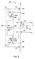
次に図6を参照する。図6は別のチャージポンプ650の概略回路図である。チャージポンプ650もまた、図4のチャージポンプといくつかの点では同様であるが、さらに別の実施形態に係るクランプ654を備える。ここで図示し説明した他のクランプのように、クランプ654は、VbiaspとVbiasnとによって定義される限界の範囲内にVcを制限しない。
Reference is now made to FIG. FIG. 6 is a schematic circuit diagram of another
図示したクランプ654は、ゲート657に信号PUが印加されたNMOSトランジスタ656と、ゲート659に信号PDが印加されたPMOSトランジスタ658と、アナログ中継器660とを備える。中継器660の入力662はノード130に接続されているのに対し、中継器660の出力664は、トランジスタ656のソース666とトランジスタ658のソース668とに電気的に接続されている。
The illustrated
図示したクランプ654内では、トランジスタ656はスイッチング・トランジスタ104と動作連動している。特に、トランジスタ656のドレイン670は、ノード672を介してスイッチング・トランジスタ104に電気的に接続されている。それに加えて、トランジスタ658は、スイッチング・トランジスタ108と動作連動している。特に、トランジスタ658のドレイン674は、ノード676を介してスイッチング・トランジスタ108に電気的に接続されている。
Within the illustrated
当業者に理解されるように、ロジックハイ信号がゲート657に印加される結果、トランジスタ656は、オフに切り替わっている間に導通を開始する。このように、トランジスタ656が導通していることから、中継器660が供給するVc電圧の複製がノード672に連結される。漏れ電流経路全域に渡って電圧降下が小さく、またノード672における電圧は、トランジスタ104がオフに切り替わっている間その値が大きく下がらないようになっているため、漏れ電流は最小限に留められる。また、オフに切り替わる時に生成される寄生電流スパイクは、スイッチング・トランジスタ104とキャパシタ102との間の経路を部分的にしか通らない(トランジスタ656が導通している時、ノード672を通る追加電流経路が再び提供される)。
As will be appreciated by those skilled in the art, as a result of the logic high signal being applied to
同様に、ロジックハイ信号がゲート659に印加されるため、トランジスタ658はトランジスタ108がオフに切り替わっている間に、導通を開始する。トランジスタ656が導通しているため、中継器660が供給するVc電圧の複製がノード676に連結される。ここでも、漏れ電流経路全域に渡って電圧差が小さく、またノード676における電圧は、トランジスタ108がオフに切り替わっている間大きく上昇しないようになっているため、漏れ電流は最小限に留められる。さらに、オフに切り替わる時に生成される寄生電流スパイク(回路のシンク部)は、スイッチング・トランジスタ108とキャパシタ102との間の経路を部分的にしか通らない(トランジスタ658が導通している場合、ノード676を通る追加電流経路が再び提供される)ことが再度分かるだろう。
Similarly, since a logic high signal is applied to
いくつかの例では、中継器660は存在しない。例えば、ノード672及び676は、トランジスタ104及び108がオフに切り替わっている状態の間、ノード130に直接連結され得る。しかしながら、そのような場合には連結時電荷注入が起こる。特に、トランジスタ656及び658の寄生容量は、ノード130への連結時電荷注入の原因となる。
In some examples,
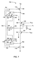
今度は図7を参照する。図7は、別のチャージポンプ700の概略回路図である。チャージポンプ700は、さらに別の実施形態に係るクランプ704を備える。チャージポンプ700は、上記で図示し説明した他のチャージポンプといくつかの点では同様である。例えばここで図示し説明した多くの他のクランプのように、クランプ704は、VbiaspとVbiasnとによって定義される限界の範囲内にVcを制限しない。
Reference is now made to FIG. FIG. 7 is a schematic circuit diagram of another
図示したクランプ704は、2つのインバータ706及び708と、PMOSトランジスタ710と、NMOSトランジスタ712と、アナログ中継器714とを備える。回路構成で言えば、インバータ706の入力716には信号PUが供給され、インバータ706の出力718はトランジスタ710のゲート720に印加される。同様に、インバータ708の入力724には信号PDが供給され、インバータ708の出力728は、トランジスタ712のゲート732に印加される。また、中継器714の入力736はノード130に接続されているのに対し、中継器714の出力740はトランジスタ710のドレイン744とトランジスタ712のドレイン748とに電気的に接続されている。
The illustrated
図示したクランプ704内では、トランジスタ710はスイッチング・トランジスタ104と動作連動している。特に、トランジスタ710のドレイン752は、ノード756を介してスイッチング・トランジスタ104に電気的に接続されている。それに加えて、トランジスタ712はスイッチング・トランジスタ108と動作連動している。特に、トランジスタ712のドレイン760は、ノード764を介してスイッチング・トランジスタ108に電気的に接続されている。
Within the illustrated
図7のクランプ704は、図6のクランプ654と動作上同様であることが分かるであろう。繰り返しになるが、図示した中継器は全ての例で存在しているわけではない。
It will be appreciated that the
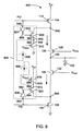
今度は図8を参照する。図8は、別のチャージポンプ800の概略回路図である。チャージポンプ800は、さらに別の実施形態に係るクランプ804を備える。ここでも、チャージポンプ800は、先に図示し説明した他のチャージポンプといくつかの点では同様であることが分かる。例えば、ここで図示し説明した多くの他のクランプのように、クランプ804は、VbiaspとVbiasnとによって定義される限界の範囲内にVcを制限しない。
Reference is now made to FIG. FIG. 8 is a schematic circuit diagram of another charge pump 800. The charge pump 800 includes a
図示したクランプ804は、一対のPMOSトランジスタ808及び812と、一対のNMOSトランジスタ816及び820と、2つのインバータ824及び828とを備える。トランジスタ808と、トランジスタ812と、インバータ824とを備えるクランプ804の半分は、スイッチング・トランジスタ104と動作連動しており、トランジスタ816と、トランジスタ820と、インバータ828とを備えるクランプ804の他の半分は、スイッチング・トランジスタ108と動作連動している。
The illustrated
スイッチング・トランジスタ104と動作連動している図示したクランプ804の半分に関し、トランジスタ808のソース832は、ノード836を介してスイッチング・トランジスタ104に電気的に接続されている。また、トランジスタ808のドレイン840は、トランジスタ812のソース844に電気的に接続されており、ドレイン840とソース844との間にあるノードにおける電圧は、接地電位までは低下しない。インバータ824の入力848とトランジスタ104のゲート112には、同じ信号、即ちPUが印加される。インバータ824の出力856は、トランジスタ808のゲート860に電気的に接続されている。トランジスタ812のゲート862には信号Vbiasp1が印加される。(少なくともいくつかの例では、Vbiasp1はVbiaspと同様のまたは実質的に同じ値を有する。)
スイッチング・トランジスタ108と動作連動している図示したクランプ804の半分に関し、トランジスタ820のソース864は、ノード868を介してスイッチング・トランジスタ108に電気的に接続されている。また、トランジスタ820のドレイン872は、トランジスタ816のソース876に電気的に接続されており、ドレイン872とソース876との間にあるノードにおける電圧は、Vddまでは上昇しない。インバータ828の入力880とトランジスタ108のゲート116とには、同じ信号、即ちPDが印加される。インバータ828の出力882は、トランジスタ820のゲート884に電気的に接続されている。トランジスタ816のゲート894には、信号Vbiasn1が印加される。(少なくともいくつかの例では、Vbiasn1はVbiaspと同様のまたは実質的に同じ値を有する。)
引き続きスイッチング・トランジスタ108と動作連動している図示したクランプ804の半分を参照すれば、トランジスタ108がオフに切り替わっている間、トランジスタ820は導通を開始し、ノード868と、ドレイン872とソース876との間にあるノードとの間での電荷交換が行われる(例えば、トランジスタ816と820の寄生容量は、お互いに電荷を交換する)ことが分かる。トランジスタ816の大きさとVbiasn1の値を適切に選択することで、トランジスタ108がオフに切り替わった時にノード868における電圧レベルを上昇させるようにでき、それによりテールアウト電流を急速にカットオフできる。特に、当該電圧遷移は、大体、Vbiasn−VT#nからVbiasn1−VT#n1までの範囲である。また、クランプ804は、ノード868における電圧がVbiasn1−VT#n1より低くならないよう制限する。ノード868における電圧がVbiasn−VT#nより低くならない限り、漏れ電流は微量しか存在しないため、クランプ804は、スイッチング・トランジスタ108がオフに切り替わっている間、ノード868における電圧を効果的にVbiasn1−VT#n1近辺で維持する。
With respect to half of the illustrated
With respect to the half of the illustrated
With continued reference to half of the illustrated
スイッチング・トランジスタ104と動作連動している図示したクランプ804の半分を参照すれば、トランジスタ104がオフに切り替わる時に、トランジスタ808は導通を開始し、ノード836と、ドレイン840とソース844との間にあるノードとの間の電荷交換が行われる(例えば、トランジスタ808と812の寄生容量はお互いに電荷を交換する)ことが分かる。トランジスタ812の大きさとVbiasp1の値を適切に選択することで、トランジスタ104がオフに切り替わった時に、ノード836における電圧レベルは、テールアウト電流を急速にカットオフさせるのに十分なほど大きく低下する。特に、当該電圧遷移は、大体、Vbiasp+VT#pからVbiasp1+VT#p1までの範囲である。また、クランプ804は、ノード836における電圧がVbiasp1+VT#p1より大きくならないよう制限する。ノード836における電圧がVbiasp+VT#pより大きくなっている限り、漏れ電流は微量しか存在しないため、クランプ804は、スイッチング・トランジスタ104がオフに切り替わっている間、ノード836における電圧を、効果的にVbiasp1+VT#p1の近辺で維持する。
Referring to half of the illustrated
図8に示した実施形態に関して、一点捕捉する。いずれかのスイッチング・トランジスタがオフに切り替わった時に、漏れ電流経路は存在する。特に、漏れ電流経路は、i)トランジスタ120、808、及び812を通る経路であり、ii)トランジスタ124、820、及び816を通る経路である。しかしながら、漏れ電流は、例えば図3に示すチャージポンプ300に比べて小さい。また、クランプ804は、スイッチング・トランジスタがオフに切り替わっている間にノード836及び868における電圧を一定の値近辺で維持することを更に確実にするために、非常に小さな電流源896及び898を任意で備えてもよい。これらの電流源は、寄生容量による小さな電流を等しく打ち消す。一例において、電流源896は、PMOSトランジスタ(PMOSトランジスタのソースとゲートは、それぞれVddとVbiaspに接続された状態)を用いて実現され、電流源898は、NMOSトランジスタ(NMOSトランジスタのソースとゲートは、それぞれ接地電位とVbiasnに接続された状態)を用いて実現される。
A single point is captured for the embodiment shown in FIG. A leakage current path exists when any switching transistor is switched off. In particular, the leakage current path is i) a path through
今度は図9を参照する。図9は、別のチャージポンプ900の概略回路図である。チャージポンプ900は、さらに別の実施形態に係るクランプ904を備える。ここでも、チャージポンプ900は、先に図示し説明した他のチャージポンプといくつかの点では同様であることが分かる。例えば、ここで図示し説明した多くの他のクランプのように、クランプ904は、VbiaspとVbiasnとによって定義される限界の範囲内にVcを制限しない。
Reference is now made to FIG. FIG. 9 is a schematic circuit diagram of another
図示したクランプ904は、PMOSトランジスタ908と、NMOSトランジスタ920と、2つのインバータ924及び928とを備える。トランジスタ908とインバータ924とを備えるクランプ904の半分は、スイッチング・トランジスタ104と動作連動しており、トランジスタ920とインバータ928とを備えるクランプ904の他の半分は、スイッチング・トランジスタ108と動作連動している。
The illustrated
スイッチング・トランジスタ104と動作連動している図示したクランプ904の半分に関し、トランジスタ908のソース932は、ノード936を介してスイッチング・トランジスタ104に電気的に接続されている。また、トランジスタ908のドレイン940には信号Vbiaspが印加される。インバータ924の入力948とトランジスタ104のゲート112には同じ信号、即ちPUが印加される。インバータ924の出力956はトランジスタ908のゲート960に電気的に接続されている。
With respect to half of the illustrated
スイッチング・トランジスタ108と動作連動している図示したクランプ904の半分に関し、トランジスタ920のソース964は、ノード968を介してスイッチング・トランジスタ108に電気的に接続されている。また、トランジスタ920のドレイン972には信号Vbiasnが印加される。インバータ928の入力980とトランジスタ108のゲート116には同じ信号、即ちPDが印加される。インバータ928の出力982は、トランジスタ920のゲート984に電気的に接続されている。
With respect to the half of the illustrated
クランプ904の動作は、図8に示すクランプ804の動作と同様である。2つのクランプの主な違いは、クランプ904にはトランジスタ812、816、及びそれらトランジスタのゲートに印加される対応するバイアス電圧がない点である。その代わり、トランジスタ908のドレイン940はVbiaspに連結され、同様にトランジスタ920のドレイン972はVbiasnに連結されている。
The operation of the
今度は図10を参照する。図10は、別のチャージポンプ1000の概略回路図である。チャージポンプ1000は、さらに別の実施形態に係るクランプ1004を備え、クランプ1004はNMOSトランジスタ1008とPMOSトランジスタ1012とを備える。ここでも、チャージポンプ1000は、先に図示し説明した他のチャージポンプといくつかの点では同様であることが分かる。例えば、ここで図示し説明した多くの他のクランプのように、クランプ1004は、VbiaspとVbiasnとによって定義される限界の範囲内にVcを制限しない。また、クランプ1004は、図9に示すクランプ904と特に同様であり、2つのクランプの主な違いは、PMOSトランジスタ908がNMOSトランジスタに置き換えられ、NMOSトランジスタ920がPMOSトランジスタに置き換えられたことによりインバータが排除された点である。
Reference is now made to FIG. FIG. 10 is a schematic circuit diagram of another
NMOSトランジスタ1008に関し、このトランジスタは、スイッチング・トランジスタ104と動作連動している。特に、トランジスタ1008のドレイン1016はノード1020を介してスイッチング・トランジスタ104に電気的に接続されている。また、トランジスタ1008のドレイン1024には信号Vbiaspが印加される。トランジスタ1008のゲート1028及びトランジスタ104のゲート112には同じ信号、即ちPUが印加される。
With respect to
PMOSトランジスタ1012に関して、このトランジスタは、スイッチング・トランジスタ108と動作連動している。トランジスタ1012のドレイン1032は、ノード1036を介してスイッチング・トランジスタ108に電気的に接続されている。また、トランジスタ1012のソース1040には信号Vbiasnが印加されている。トランジスタ1012のゲート1044及びトランジスタ108のゲート116には同じ信号、即ちPDが印加される。
With respect to PMOS transistor 1012, this transistor is operatively associated with switching transistor. The
いくつかの用途では、クランプ1004の効果は、より大きなトランジスタを用いることで向上し得る(即ち、トランジスタ1008及び/またはトランジスタ1012の大きさを大きくする)。
In some applications, the effectiveness of
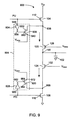
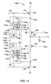
今度は図11を参照する。図11は、別のチャージポンプ1100の概略回路図である。チャージポンプ1100は、さらに別の実施形態に係るクランプ1104を備える。ここでも、チャージポンプ1100は、先に図示し説明した他のチャージポンプといくつかの点では同様であることが分かる。例えば、ここで図示し説明した多くの他のクランプのように、クランプ1104は、VbiaspとVbiasnとによって定義される限界の範囲内にVcを制限しない。
Reference is now made to FIG. FIG. 11 is a schematic circuit diagram of another
図示したクランプ1104は、一対のNMOSトランジスタ1108及び1112と、一対のPMOSトランジスタ1116及び1120と、遅延導入インバータ回路(またはインバータ)1124と、別の遅延導入インバータ回路1128と、2つの付加的なトランジスタ1132及び1136とを備える。
The illustrated
図示した実施形態において、トランジスタ1108、1112、1132とインバータ1124とを備えるクランプ1104の半分は、スイッチング・トランジスタ104と動作連動しており、トランジスタ1116、1120、1136とインバータ1128とを備えるクランプ1104の他の半分は、スイッチング・トランジスタ108と動作連動している。
In the illustrated embodiment, half of
スイッチング・トランジスタ104と動作連動している図示したクランプ1104の半分に関して、トランジスタ1108のドレイン1140は、ノード1144を介してスイッチング・トランジスタ104に電気的に接続されている。また、トランジスタ1108のソース1148は、トランジスタ1132のゲート1156、並びにトランジスタ1112のドレイン1152に電気的に接続されている。インバータ1124の入力1160とトランジスタ1108のゲート1164の双方には、同じ信号、即ちPUが印加される。インバータ1124の出力1168は、トランジスタ1112のゲート1180、並びにトランジスタ1132のソース1172とドレイン1176の双方に電気的に接続されている。
With respect to half of the illustrated
スイッチング・トランジスタ108と動作連動している図示したクランプ1104の半分に関して、トランジスタ1120のドレイン1181は、ノード1182を介してスイッチング・トランジスタ108に電気的に接続されている。また、トランジスタ1120のソース1184は、トランジスタ1116のドレイン1185に電気的に接続されている。インバータ1128の入力1187と、トランジスタ1120のゲート1188の双方には、同じ信号、即ちPDが印加される。インバータ1128の出力1190は、トランジスタ1116のゲート1196、並びにトランジスタ1136のドレイン1192とソース1192の双方に電気的に接続されている。
With respect to half of the illustrated
クランプ1104の動作は、図4に示すクランプ504の動作と同様である。しかしながら、クランプ1104は、キャパシタ内蔵装置として構成された付加的なトランジスタ1132と1136を備える。トランジスタ1132はキャパシタとして機能し、トランジスタ104がオフに切り替わっている間に、ノード1144に付加的な電荷を注入する。トランジスタ1136もキャパシタとして機能し、トランジスタ108がオフに切り替わっている間に、ノード1182から付加的な電荷を減らすという機能を果たす。トランジスタ1132と1136は、それらのプレート全体に渡る電圧の低下がトランジスタのしきい値電圧よりも小さくならないので、標準外である必要がないことが分かるだろう。
The operation of the
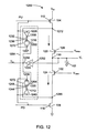
今度は図12を参照する。図12は、別のチャージポンプ1200の概略回路図である。チャージポンプ1200は、さらに別の実施形態に係るクランプ1204を備える。チャージポンプ1200は、先に図示し説明した他のチャージポンプといくつかの点にでは同様であることが分かる。例えば、ここで図示し説明した多くのクランプのように、クランプ1204は、VbiaspとVbiasnとによって定義される限界の範囲内にVcを制限しない。
Reference is now made to FIG. FIG. 12 is a schematic circuit diagram of another
図示したクランプ1204は、2つのインバータ1208及び1212と、2つの伝送ゲート1216及び1220と、アナログ中継器1224とを備える。回路構成で言えば、信号PUは、伝送ゲート1216の制御入力1227とインバータ1208の入力1228の双方に入力され、インバータ1208の出力1232は、伝送ゲート1216の制御入力1236に供給される。同様に、信号PDは、伝送ゲート1220の制御入力1239とインバータ1212の入力1240の双方に入力され、インバータ1212の出力1244は、伝送ゲート1220の制御入力1248に供給される。また、中継器1224の入力1252はノード130に接続されているのに対し、中継器1224の出力1256は、伝送ゲート1216及び1220のそれぞれの入力1260及び1264に電気的に接続されている。
The illustrated
図示したクランプ1204内では、伝送ゲート1216は、スイッチング・トランジスタ104と動作連動している。特に、伝送ゲート1216の出力1270は、ノード1272を介してスイッチング・トランジスタ104に電気的に接続されている。さらに伝送ゲート1220は、スイッチング・トランジスタ108と動作連動している。特に伝送ゲート1220の出力1272は、ノード1285を介してスイッチング・トランジスタ108に電気的に接続されている。
Within the illustrated
トランジスタ104がオフに切り替わっている間、伝送ゲート1216は導通を開始し、それによりノード1272は中継器1224の出力1256におけるノードと連結する(Vcsノード)。漏れ電流経路全体に渡って電圧低下が小さく、またトランジスタ104がオフに切り替わっている間、ノード1272における電圧は、その値が大きく低下しないようにされているため、漏れ電流は最小限に留められる。また、オフに切り替わる時に発生する寄生電流スパイクは、スイッチング・トランジスタ104とキャパシタ102との間の経路を部分的にしか流れない(伝送ゲート1216が導通している間、ノード1272を通る追加電流経路が提供される)。
While
同様に、トランジスタ108がオフに切り替わっている間、伝送ゲート1220は導通を開始し、ノード1285をVcsノードに連結させる。複製電圧Vcsは複製されるべき電圧Vcに非常に近いため、ノード1285(またはノード1272)はスイッチング・トランジスタがオフに切り替わった時には、Vcに近い電圧値を有するノードに連結される。よって漏れ経路全体に渡って電圧の低下は、漏れが最小限となるのに十分なほど小さくなる。ここでも、オフに切り替わる時に発生する寄生電流スパイク(回路のソース部)は、スイッチング・トランジスタ108とキャパシタ102との間の経路を部分的にしか流れない(伝送ゲート1220が導通している間、ノード1285を通る追加電流経路が提供される)。
Similarly, while
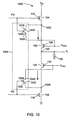
今度は図13を参照する。図13は、別のチャージポンプ1300の概略回路図である。チャージポンプ1300は、さらに別の実施形態に係るクランプ1304を備える。チャージポンプ1300は、先に図示し説明した他のチャージポンプといくつかの点にでは同様であることが分かる。例えば、ここで図示し説明した多くの他のクランプのように、クランプ1304は、VbiaspとVbiasnとによって定義される限界の範囲内にVcを制限しない。
Reference is now made to FIG. FIG. 13 is a schematic circuit diagram of another
図示したクランプ1304は、2つのインバータ1308及び1312と、2つの伝送ゲート1316及び1320と、2つのトランジスタ1324及び1328とを備える。回路構成の点において、信号PUは、伝送ゲート1316の制御入力1330とインバータ1308の入力1332の双方に入力され、インバータ1308の出力1334は、伝送ゲート1316の制御入力1336に印加される。同様に、信号PDは、伝送ゲート1320の制御入力1340とインバータ1312の入力1342の双方に入力され、インバータ1312の出力1344は、伝送ゲート1320の制御入力1346に印加される。
The illustrated
図示したクランプ1304内では、伝送ゲート1316は、スイッチング・トランジスタ104と動作連動している。特に、伝送ゲート1316の出力1349は、ノード1350を介してスイッチング・トランジスタ104に電気的に接続されていおり、NMOSトランジスタ1324がオンの状態で、かつ伝送ゲート1316が導通している時に、ノード1350と接地との間にオープンパスが存在する。さらに、伝送ゲート1320は、スイッチング・トランジスタ108と動作連動している。特に、伝送ゲート1320の出力1352は、ノード1354を介してスイッチング・トランジスタ108に電気的に接続されており、PMOSトランジスタ1328がオンにされ、かつ伝送ゲート1320が導通している時に、ノード1354とVddとの間にオープンパスが存在する。
Within the illustrated
トランジスタ104がオフに切り替わっている間、伝送ゲート1316は導通を開始し、それによりノード1350は、伝送ゲート1316の入力1382とトランジスタ1324のドレイン1384との間に位置するノード1380に連結される。このオフに切り替わっている時、ノード1380の電位は概ね接地電位であり、ノード1350における電圧が急速に低下してテイルアウト電流がカットオフされる間にノード1380と1350との間で電荷交換が起こる。また、この電荷交換が起こっている時に、寄生電流スパイクがスイッチング・トランジスタ104とキャパシタ102との間の経路を部分的にだけ通るように、ノード1350を通る追加経路が提供される。漏れ電流の流れがこのパッシブな状態で最小限に留められるようにノード1350における電圧が遷移する新たな電圧値は、スイッチング・トランジスタ104がオフに切り替わっている間維持される。また、漏れ経路が遮断されるようにトランジスタ1324がオフにされる。
While
同様に、トランジスタ108がオフに切り替わっている間、伝送ゲート1320は導通を開始し、それによりノード1354は、伝送ゲート1320の入力1392とトランジスタ1328のドレイン1394との間に位置するノード1390に連結される。このオフに切り替わっている時、ノード1390の電位は約Vddであり、ノード1354における電圧が急速に上昇して、テイルアウト電流がカットオフされる間にノード1390と1354との間で電荷交換が起こる。また、この電荷交換が起こっている時に、寄生電流スパイクがスイッチング・トランジスタ108とキャパシタ102との間の経路を部分的にだけ通るように、ノード1354を通る追加経路が提供される。漏れ電流の流れがこのパッシブな状態で最小限に留められるように、ノード1354における電圧が遷移する新たな電圧値は、スイッチング・トランジスタ108がオフに切り替わっている間維持される。また、漏れ経路が断線されるようにトランジスタ1328がオフにされる。
Similarly, while
今度は図14を参照する。図2と同様に、図14は電流の(経時)波形図の一例であるが、同波形図は(図1に示す回路の経路ではなく)図4に示す回路の経路を流れる電流の波形図である。一例の信号PU及びPD(及びゲート560と592から出力された信号)も、波形図の一例の上のグラフに示す。
Reference is now made to FIG. As in FIG. 2, FIG. 14 is an example of a current (time) waveform diagram, but the waveform diagram is a waveform diagram of current flowing through the circuit path shown in FIG. 4 (not the circuit path shown in FIG. 1). It is. An example signal PU and PD (and signals output from
今度は図4及び図14を参照して、時間tc1(トランジスタ108がオフに切り替わるのが始まる点に対応)から始まり時間tc2で終わる期間の間、ロジックローの値(PMOSトランジスタのゲートに印加された場合オン状態を作り出す)がトランジスタ516と520の両方のゲートに印加されることが分かる。よって、短い時間の間、一対のトランジスタ516と520は、トランジスタ108からのオフスイッチング電流に対して追加経路を提供する。しかしながら、他の時間では、トランジスタ516と520のうちの少なくとも1つはオフにされ、そのためそのような場合においては追加経路は提供されないことが分かる。クランプ504のソース部を構成する一対のトランジスタ(即ち、トランジスタ508及び512)に関して、それらは同様に機能する。しかしながら、当業者に理解されるように、NMOSトランジスタのゲートに印加された場合にオン状態を作り出すのは(ロジックローよりも)ロジックハイの値である。
Now referring to FIGS. 4 and 14, during the period starting from time t c1 (corresponding to the point where
今度は図2の電流IpとInのグラフと、図14の電流IpとInのグラフを比較する。その場合、クランプ504の効果は明らかである。特に、スイッチング・トランジスタ104がオフに切り替わった時に、電流Ip'には非常に小さい上向きスパイク694しかないことが分かる。同様に、スイッチング・トランジスタ108がオフに切り替わった時に、時間tc2では非常に小さな下向きスパイク696しかないことが分かる。時間tc1の後、電流Ip'とIn'は約0μAまで急速に低下するため、クランプ504がテイルアウト電流の急速なカットアウトに対して影響を与えることは波形図からも明らかである。図5〜13に示すクランプのシミュレーション結果も同様である(極めて小さな電流スパイク、テイルアウト電流の急速なカットオフ)。
Now comparing the graphs of the current I p and I n of FIG. 2, a graph of current I p and I n of FIG. In that case, the effect of the
添付の図面に示すチャージポンプは、ソース部及びシンク部の双方を有するが、いくつかの例ではチャージポンプはソース部またはシンク部のいずれかしか有していないこともある。また、図示した実施形態の回路におけるトランジスタはFETであるが、ここに含まれる教示は、例えば、バイポーラトランジスタ等の他の種類のトランジスタからなるクランプを有するチャージポンプを実現するための指示を提供していることが分かる。図15及び図16を参照すると、それらはクランプ1504及び1604をそれぞれ含む一例としてのチャージポンプ1500及び1600の概略回路図である。チャージポンプ1500及び1600はそれぞれ概念的には図4及び5のチャージポンプと同様であるが、それらはFETではなくバイポーラトランジスタからなる。
Although the charge pump shown in the accompanying drawings has both a source portion and a sink portion, in some instances the charge pump may have only a source portion or a sink portion. Also, although the transistors in the circuit of the illustrated embodiment are FETs, the teachings contained herein provide instructions for implementing a charge pump having a clamp comprised of other types of transistors, such as bipolar transistors. I understand that Referring to FIGS. 15 and 16, they are schematic circuit diagrams of exemplary charge pumps 1500 and 1600 that include
説明した実施形態のある程度の改造及び変更を行うことができる。従って、上記の実施形態は説明に役立てるためのものであって、制限するものではないと考えられるべきである。 Certain modifications and variations of the described embodiments can be made. Therefore, it should be understood that the above-described embodiments are intended to be illustrative and not limiting.
Claims (30)
その値が第1の値から第2の値に変化した時に、前記少なくとも1つのトランジスタをオフに切り替わらせる少なくとも1つの制御信号を供給する工程と、
前記少なくとも1つの寄生スパイクが、前記第1及び第2の経路の内の選択された一方を通って部分的にだけ伝達されるように、前記少なくとも1つの制御信号の値が前記第1の値から前記第2の値に変化した時に、前記少なくとも1つのトランジスタからの電流に対する追加経路を形成する工程と、
前記追加経路が前記短い期間の間形成された後に、前記追加経路を解消させる工程とを含む方法。 A charge pump comprising a switching circuit and a capacitor, wherein a current is supplied to the capacitor and forms a first path and a second path through which a current flows when the current is supplied from the capacitor. At least one parasitic spike in the current from at least one of the transistors is generated while the at least one transistor is switched off, and the at least one parasitic spike disappears after a short period of time has elapsed. A method of clamping current in a charge pump, wherein the method is:
Providing at least one control signal to switch the at least one transistor off when the value changes from a first value to a second value;
The value of the at least one control signal is the first value such that the at least one parasitic spike is only partially transmitted through a selected one of the first and second paths. Forming an additional path for current from the at least one transistor when changing from to a second value;
Removing the additional path after the additional path is formed for the short period of time.
第1及び第2の対のトランジスタを備え、同トランジスタの各々はオン及びオフ状態をサポートし、前記状態間の遷移を制御する制御電極を備え、前記第1の対のトランジスタの内の一方は、第1のノードを介して前記スイッチング回路のトランジスタの内の最初のトランジスタに電気的に接続され、前記第1の経路は前記第1のノードを通って伸びており、前記第2の対のトランジスタの内の一方は、第2のノードを介して前記スイッチング回路のトランジスタの内の二番目のトランジスタに電気的に接続され、前記第2の経路は前記第2のノードを通って伸びており、
同回路はさらに、
第1の遅延導入インバータ回路と、
第2の遅延導入インバータ回路とを備え、前記第1のインバータ回路及び前記第2のインバータ回路の各々は、前記それぞれの対のトランジスタの内の一方の制御電極に入力される信号を入力信号とし、前記それぞれの対のトランジスタの内の他方の制御電極に遅延出力信号を供給し、前記オフへの切り替えが起こる瞬間、前記入力信号と前記遅延出力信号の双方は、前記オン状態を作り出す値を有し、
前記第1及び第2の対のトランジスタの内の少なくとも一方は、前記少なくとも1つの寄生スパイクが、前記キャパシタに向かういずれかの経路を通って部分的にだけ伝達されるように、前記オフに切り替わっている間、前記トランジスタの内の前記少なくとも1つからの電流に対する追加経路を形成することを特徴とする回路。 A charge pump comprising a switching circuit and a capacitor, wherein a current is supplied to the capacitor and forms a first path and a second path through which a current flows when the current is supplied from the capacitor. A circuit that clamps current in a charge pump in which at least one parasitic spike in current from at least one of the transistors is generated while the at least one transistor is switched off, the circuit comprising: ,
A first and second pair of transistors, each of which supports an on and off state and includes a control electrode that controls transitions between the states, one of the first pair of transistors being , Electrically connected to the first of the transistors of the switching circuit through a first node, the first path extending through the first node, and the second pair of transistors One of the transistors is electrically connected to a second transistor of the transistors of the switching circuit through a second node, and the second path extends through the second node. ,
The circuit further
A first delay introducing inverter circuit;
A second delay-introducing inverter circuit, and each of the first inverter circuit and the second inverter circuit has a signal input to one control electrode of the pair of transistors as an input signal. , Supplying a delayed output signal to the other control electrode of each of the pair of transistors, and at the instant when the switch-off occurs, both the input signal and the delayed output signal have values that create the on state. Have
At least one of the first and second pairs of transistors switches off such that the at least one parasitic spike is only partially transmitted through any path toward the capacitor. A circuit for forming an additional path for current from the at least one of the transistors.
その値が第1の値から第2の値に変化した時に、前記スイッチングトランジスタをオフに切り替わらせる制御信号を供給する入力とを備える装置であって、
前記電流クランプ回路は、(i)前記少なくとも1つの寄生スパイクが、前記第1及び第2の経路の内の前記一方を通って部分的にだけ伝達されるように、前記制御信号の値が前記第1の値から前記第2の値に変化した時に、前記スイッチングトランジスタからの電流に対する追加経路を形成し、(ii)前記追加経路が前記短い期間の間形成された後に、前記追加経路を解消させるためのものであることを特徴とする装置。 A plurality of switching transistors, a current clamp circuit, and a capacitor, wherein a first path and a second path through which current is supplied to the capacitor and when current is supplied from the capacitor are formed; One of the transistors is located in a selected one of the first and second paths, and when the switching transistor switches off, it generates a parasitic spike in the current, A charge pump that disappears after a short period of time,
And an input for supplying a control signal for switching the switching transistor off when the value changes from a first value to a second value,
The current clamp circuit has (i) the value of the control signal is such that the at least one parasitic spike is only partially transmitted through the one of the first and second paths. Forming an additional path for the current from the switching transistor when changing from a first value to the second value; (ii) eliminating the additional path after the additional path is formed for the short period of time A device characterized in that it is for making
その値が第1の値から第2の値に変化した時に、前記少なくとも1つのトランジスタをオフに切り替わらせる少なくとも1つの制御信号を供給する工程と、
前記少なくとも1つの寄生スパイクが、前記第1及び第2の経路の内の選択された一方を通って部分的にだけ伝達されるように、前記少なくとも1つの制御信号の値が前記第1の値から前記第2の値に変化した時に、前記少なくとも1つのトランジスタからの電流に対する追加経路を形成し、前記追加経路は第1のノードを介して前記少なくとも1つのトランジスタに提供され、前記少なくとも1つのトランジスタがオフに切り替わっている間に前記第1のノードにおける電圧の値は変化する工程と、
前記少なくとも1つのトランジスタがオフに切り替わった後に、前記第1及び第2の経路の内の前記一方におけるトランジスタを流れる漏れ電流を、前記キャパシタを基準として最小限にする工程とを含む方法。 A charge pump comprising a switching circuit and a capacitor, wherein a current is supplied to the capacitor and forms a first path and a second path through which a current flows when the current is supplied from the capacitor. A method of clamping current in a charge pump in which at least one parasitic spike in current from at least one of the transistors is generated while the at least one transistor is switched off, the method comprising: ,
Providing at least one control signal to switch the at least one transistor off when the value changes from a first value to a second value;
The value of the at least one control signal is the first value such that the at least one parasitic spike is only partially transmitted through a selected one of the first and second paths. Forming an additional path for the current from the at least one transistor when changing from to a second value, the additional path being provided to the at least one transistor via a first node, Changing the value of the voltage at the first node while the transistor is switched off;
Minimizing leakage current through the transistor in the one of the first and second paths after the at least one transistor is turned off with respect to the capacitor.
その値が第1の値から第2の値に変化した時に、前記スイッチングトランジスタをオフに切り替わらせる制御信号を供給する入力とを備える装置であって、
前記電流クランプ回路は、(i)前記寄生スパイクが、前記第1及び第2の経路の内の前記一方を通って部分的にだけ伝達されるように、前記制御信号の値が前記第1の値から前記第2の値に変化した時に、前記スイッチングトランジスタからの電流に対する追加経路を形成し、前記追加経路は前記第1のノードを介して前記スイッチングトランジスタに提供され、前記スイッチングトランジスタがオフに切り替わっている間、前記第1のノードにおける電圧の値は変化し、(ii)前記少なくとも1つのトランジスタがオフに切り替わった後に、前記第1及び第2の経路の内の前記一方におけるトランジスタを流れる漏れ電流を、前記キャパシタを基準として最小限にするためのものであることを特徴とする装置。 A plurality of switching transistors, a current clamp circuit, and a capacitor, wherein a first path and a second path through which current is supplied to the capacitor and when current is supplied from the capacitor are formed; A charge pump for generating a parasitic spike in the current when one of the transistors and the first node are located in a selected one of the first and second paths and the switching transistor is switched off; ,
And an input for supplying a control signal for switching the switching transistor off when the value changes from a first value to a second value,
The current clamp circuit includes: (i) the value of the control signal is the first value so that the parasitic spike is only partially transmitted through the one of the first and second paths. When changing from a value to the second value, an additional path for the current from the switching transistor is formed, the additional path being provided to the switching transistor via the first node, the switching transistor being turned off While switching, the value of the voltage at the first node changes and (ii) flows through the transistor in the one of the first and second paths after the at least one transistor is switched off. An apparatus for minimizing leakage current with respect to the capacitor.
Applications Claiming Priority (3)
| Application Number | Priority Date | Filing Date | Title |
|---|---|---|---|
| US11/606,827 | 2006-11-30 | ||
| US11/606,827 US7915933B2 (en) | 2006-11-30 | 2006-11-30 | Circuit for clamping current in a charge pump |
| PCT/CA2007/002113 WO2008064464A1 (en) | 2006-11-30 | 2007-11-26 | Circuit for clamping current in a charge pump |
Related Child Applications (1)
| Application Number | Title | Priority Date | Filing Date |
|---|---|---|---|
| JP2012254359A Division JP5575862B2 (en) | 2006-11-30 | 2012-11-20 | Circuit to clamp current in charge pump |
Publications (3)
| Publication Number | Publication Date |
|---|---|
| JP2010511368A true JP2010511368A (en) | 2010-04-08 |
| JP2010511368A5 JP2010511368A5 (en) | 2012-03-08 |
| JP5199270B2 JP5199270B2 (en) | 2013-05-15 |
Family
ID=39467379
Family Applications (3)
| Application Number | Title | Priority Date | Filing Date |
|---|---|---|---|
| JP2009538559A Expired - Fee Related JP5199270B2 (en) | 2006-11-30 | 2007-11-26 | Circuit to clamp current in charge pump |
| JP2012254359A Expired - Fee Related JP5575862B2 (en) | 2006-11-30 | 2012-11-20 | Circuit to clamp current in charge pump |
| JP2014136556A Pending JP2014180213A (en) | 2006-11-30 | 2014-07-02 | Circuit for clamping current in charge pump |
Family Applications After (2)
| Application Number | Title | Priority Date | Filing Date |
|---|---|---|---|
| JP2012254359A Expired - Fee Related JP5575862B2 (en) | 2006-11-30 | 2012-11-20 | Circuit to clamp current in charge pump |
| JP2014136556A Pending JP2014180213A (en) | 2006-11-30 | 2014-07-02 | Circuit for clamping current in charge pump |
Country Status (6)
| Country | Link |
|---|---|
| US (8) | US7915933B2 (en) |
| EP (1) | EP2089959A4 (en) |
| JP (3) | JP5199270B2 (en) |
| KR (1) | KR101379637B1 (en) |
| TW (1) | TWI450072B (en) |
| WO (1) | WO2008064464A1 (en) |
Cited By (5)
| Publication number | Priority date | Publication date | Assignee | Title |
|---|---|---|---|---|
| JP2012080337A (en) * | 2010-10-01 | 2012-04-19 | Sony Corp | Phase comparator and clock data recovery circuit |
| JP2013247619A (en) * | 2012-05-29 | 2013-12-09 | Asahi Kasei Electronics Co Ltd | Current control circuit and pll circuit using the same |
| JP2013247618A (en) * | 2012-05-29 | 2013-12-09 | Asahi Kasei Electronics Co Ltd | Current control circuit and pll circuit using the same |
| JP2014533488A (en) * | 2011-11-10 | 2014-12-11 | クゥアルコム・インコーポレイテッドQualcomm Incorporated | System and method for stabilizing node voltage level of a charge pump |
| JP2019068118A (en) * | 2017-09-28 | 2019-04-25 | 株式会社メガチップス | Semiconductor integrated circuit and digital-analog conversion circuit, and driving method of semiconductor integrated circuit |
Families Citing this family (24)
| Publication number | Priority date | Publication date | Assignee | Title |
|---|---|---|---|---|
| US8354874B1 (en) * | 2009-05-15 | 2013-01-15 | Marvell International Ltd. | Kickback cancellation in class B type circuits using AC coupling |
| US8217691B2 (en) * | 2009-10-30 | 2012-07-10 | Texas Instruments Incorporated | Low power clocking scheme for a pipelined ADC |
| CN102957316A (en) * | 2011-08-31 | 2013-03-06 | 深圳艾科创新微电子有限公司 | Low-charge-injection charge pump and low charge injection method |
| US8598955B2 (en) * | 2012-03-30 | 2013-12-03 | Freescale Semiconductor, Inc. | Phase locked loop with adaptive loop filter |
| US8487677B1 (en) | 2012-03-30 | 2013-07-16 | Freescale Semiconductor, Inc. | Phase locked loop with adaptive biasing |
| US9356515B2 (en) | 2012-09-14 | 2016-05-31 | Freescale Semiconductor, Inc. | Power switching device, three phase bridge inverter, and method of operating a power switching device |
| US8754677B2 (en) * | 2012-10-01 | 2014-06-17 | Qualcomm Incorporated | System and method of implementing input/output drivers with low voltage devices |
| TWI499215B (en) * | 2012-10-17 | 2015-09-01 | Mstar Semiconductor Inc | Charging/discharging circuit and pll utilizing the charging/discharging circuit |
| CN103021359B (en) * | 2012-12-10 | 2015-11-25 | 京东方科技集团股份有限公司 | A kind of array base palte and drived control method thereof and display device |
| CN103490618A (en) * | 2013-08-29 | 2014-01-01 | 苏州苏尔达信息科技有限公司 | Low-leakage high-speed phase-locked loop charge pump circuit |
| US9391597B2 (en) | 2013-11-12 | 2016-07-12 | Macronix International Co., Ltd. | Boost circuit |
| CN104682701B (en) * | 2013-11-26 | 2017-04-26 | 旺宏电子股份有限公司 | Boosted circuit |
| US9614529B1 (en) | 2016-02-01 | 2017-04-04 | Qualcomm Incorporated | Input/output (I/O) driver implementing dynamic gate biasing of buffer transistors |
| JP6893325B2 (en) * | 2016-03-16 | 2021-06-23 | パナソニックIpマネジメント株式会社 | Inversion amplifier, integrator, sample hold circuit, AD converter, image sensor, and imaging device |
| CN106059573B (en) * | 2016-05-30 | 2019-03-29 | 中国电子科技集团公司第二十四研究所 | Reduce the circuit and method of the charge pump phase locking loop circuit switching signal amplitude of oscillation |
| JP6891888B2 (en) * | 2016-07-11 | 2021-06-18 | ソニーグループ株式会社 | Switching circuit, automatic gain control circuit and phase-locked loop |
| US10009019B2 (en) * | 2016-09-30 | 2018-06-26 | Texas Instruments Incorporated | Circuit and method to generate frequency proportional current |
| CN106954123B (en) * | 2017-02-24 | 2020-05-12 | 昂宝电子(上海)有限公司 | Power tube driving system and method |
| US9866234B1 (en) * | 2017-05-08 | 2018-01-09 | Qualcomm Incorporated | Digital-to-analog converter |
| CN107450650B (en) * | 2017-09-26 | 2019-03-26 | 深圳硅山技术有限公司 | A kind of electrification reset containing circuit applied to digit chip I/O port |
| US10484089B1 (en) * | 2018-04-27 | 2019-11-19 | Hewlett Packard Enterprise Development Lp | Driver assisted by charge sharing |
| US10491428B2 (en) | 2018-04-27 | 2019-11-26 | Hewlett Packard Enterprise Development Lp | Current supply for an opto-electronic device |
| CN110543207B (en) * | 2019-08-29 | 2020-10-13 | 电子科技大学 | Four-way adjustable power module for electric control scanning antenna |
| CN110968146A (en) * | 2019-12-12 | 2020-04-07 | 深圳星河半导体技术有限公司 | Charge pump circuit for phase-locked loop |
Citations (5)
| Publication number | Priority date | Publication date | Assignee | Title |
|---|---|---|---|---|
| US4591744A (en) * | 1983-02-14 | 1986-05-27 | Tokyo Shibaura Denki Kabushiki Kaisha | Transition detection circuit |
| JPH09298462A (en) * | 1996-04-30 | 1997-11-18 | Sony Corp | Pll circuit |
| US5825640A (en) * | 1997-06-30 | 1998-10-20 | Motorola, Inc. | Charge pump circuit and method |
| US6124741A (en) * | 1999-03-08 | 2000-09-26 | Pericom Semiconductor Corp. | Accurate PLL charge pump with matched up/down currents from Vds-compensated common-gate switches |
| JP2003298414A (en) * | 2002-04-03 | 2003-10-17 | Toshiba Corp | Semiconductor integrated circuit |
Family Cites Families (51)
| Publication number | Priority date | Publication date | Assignee | Title |
|---|---|---|---|---|
| US5197033A (en) * | 1986-07-18 | 1993-03-23 | Hitachi, Ltd. | Semiconductor device incorporating internal power supply for compensating for deviation in operating condition and fabrication process conditions |
| US4682047A (en) * | 1985-08-29 | 1987-07-21 | Siemens Aktiengesellschaft | Complementary metal-oxide-semiconductor input circuit |
| US5359727A (en) | 1987-04-27 | 1994-10-25 | Hitachi, Ltd. | Clock generator using PLL and information processing system using the clock generator |
| NO165606C (en) * | 1988-10-19 | 1991-03-06 | Bjoern O Thoresen | ADJUSTABLE FORM FOR CASTING OF STEP STEPS IN CONCRETE. |
| JP2879763B2 (en) | 1989-06-27 | 1999-04-05 | ソニー株式会社 | PLL charge pump circuit |
| KR950002726B1 (en) * | 1992-03-30 | 1995-03-24 | 삼성전자주식회사 | Charge-pump circuit of substrate voltage generator |
| US5359299A (en) | 1993-01-21 | 1994-10-25 | Gennum Corporation | High speed and low drift charge pump circuit |
| US5646563A (en) | 1994-07-15 | 1997-07-08 | National Semiconductor Corporation | Charge pump with near zero offset current |
| US5532636A (en) | 1995-03-10 | 1996-07-02 | Intel Corporation | Source-switched charge pump circuit |
| US5592113A (en) | 1995-03-28 | 1997-01-07 | National Semiconductor Corp. | Gradual frequency changing circuit |
| JP2877196B2 (en) | 1996-03-28 | 1999-03-31 | 日本電気株式会社 | Charge pump circuit and phase locked loop circuit having the same |
| JP3481051B2 (en) | 1996-06-19 | 2003-12-22 | 富士通株式会社 | Charge pump circuit, PLL circuit having the charge pump circuit, and semiconductor integrated circuit |
| EP0841753A3 (en) * | 1996-11-07 | 1999-12-15 | Nortel Networks Corporation | Charge pump circuit |
| US5734279A (en) | 1996-11-07 | 1998-03-31 | Northern Telecom Limited | Charge Pump Circuit |
| US5801578A (en) | 1996-12-16 | 1998-09-01 | Northern Telecom Limited | Charge pump circuit with source-sink current steering |
| JPH10190455A (en) * | 1996-12-26 | 1998-07-21 | Texas Instr Japan Ltd | Charge pump circuit |
| FR2767977A1 (en) | 1997-08-27 | 1999-02-26 | Philips Electronics Nv | Current charge pump output stage circuit |
| JP3227699B2 (en) * | 1998-07-29 | 2001-11-12 | 日本電気株式会社 | Charge pump circuit and PLL circuit having the same |
| US6329872B1 (en) | 1998-08-14 | 2001-12-11 | Nortel Networks Limited | Charge pump circuit for a phase locked loop |
| US6222402B1 (en) | 1998-09-04 | 2001-04-24 | International Business Machines Corporation | Differential charge-pump with improved linearity |
| JP3770741B2 (en) * | 1998-11-20 | 2006-04-26 | 富士通株式会社 | Semiconductor integrated circuit and method for switching source potential of transistor in semiconductor integrated circuit |
| JP3250540B2 (en) * | 1999-03-15 | 2002-01-28 | 日本電気株式会社 | PLL circuit |
| JP2000295098A (en) | 1999-04-06 | 2000-10-20 | Oki Electric Ind Co Ltd | Phase lock loop circuit |
| US6160432A (en) | 1999-04-30 | 2000-12-12 | Conexant Systems, Inc. | Source-switched or gate-switched charge pump having cascoded output |
| US6278332B1 (en) | 2000-02-15 | 2001-08-21 | Agere Systems Guardian Corp. | Charge pump for low-voltage, low-jitter phase locked loops |
| KR100374631B1 (en) | 2000-06-09 | 2003-03-04 | 삼성전자주식회사 | Charge pump circuit |
| US6316977B1 (en) | 2000-07-14 | 2001-11-13 | Pmc-Sierra, Inc. | Low charge-injection charge pump |
| US6967523B2 (en) * | 2000-11-21 | 2005-11-22 | Mosaid Technologies Incorporated | Cascaded charge pump power supply with different gate oxide thickness transistors |
| US6611160B1 (en) * | 2000-11-21 | 2003-08-26 | Skyworks Solutions, Inc. | Charge pump having reduced switching noise |
| KR100416589B1 (en) * | 2001-01-06 | 2004-02-05 | 삼성전자주식회사 | Charge pump circuit for improving switching characteristics and reducing leakage current and phase locked loop having the same |
| US6441660B1 (en) | 2001-02-02 | 2002-08-27 | Broadcom Corporation | High speed, wide bandwidth phase locked loop |
| US6483358B2 (en) | 2001-02-02 | 2002-11-19 | Broadcom Corporation | Low power, charge injection compensated charge pump |
| EP1229657A1 (en) * | 2001-02-02 | 2002-08-07 | Alcatel | Charge pump |
| US6891411B2 (en) * | 2001-03-29 | 2005-05-10 | Micron Technology, Inc. | Low injection charge pump |
| US6466078B1 (en) | 2001-05-04 | 2002-10-15 | Cypress Semiconductor Corp. | Reduced static phase error CMOS PLL charge pump |
| US20030038661A1 (en) * | 2001-07-27 | 2003-02-27 | Ramesh Chokkalingam | Apparatus to decrease the spurs level in a phase-locked loop |
| JP4608153B2 (en) | 2001-09-10 | 2011-01-05 | ルネサスエレクトロニクス株式会社 | Charge pump current correction circuit |
| US6952126B2 (en) * | 2001-09-29 | 2005-10-04 | Berkana Wireless, Inc. | Charge pump circuit for a PLL |
| US20030189463A1 (en) * | 2002-04-09 | 2003-10-09 | Walker Brett C. | Current saving technique for charge pump based phase locked loops |
| US6642759B1 (en) | 2002-09-04 | 2003-11-04 | National Semiconductor Corporation | Charge pump using switched capacitors for phase-locked loop control and method of operation |
| US6717446B1 (en) | 2002-09-16 | 2004-04-06 | National Semiconductor Corporation | High speed programmable charge-pump with low charge injection |
| US6844762B2 (en) * | 2002-10-30 | 2005-01-18 | Freescale Semiconductor, Inc. | Capacitive charge pump |
| US6825730B1 (en) | 2003-03-31 | 2004-11-30 | Applied Micro Circuits Corporation | High-performance low-noise charge-pump for voltage controlled oscillator applications |
| US20040257162A1 (en) * | 2003-06-23 | 2004-12-23 | Mokeddem Hadj L. | Charge pump for eliminating dc mismatches at common drian nodes |
| JPWO2005008895A1 (en) * | 2003-07-18 | 2006-09-07 | 富士通株式会社 | Charge pump circuit |
| TWI227633B (en) * | 2003-12-11 | 2005-02-01 | Vxis Technology Corp | Video clamping system using charge pump |
| EP1692767B1 (en) * | 2003-12-11 | 2019-02-27 | Conversant Intellectual Property Management Inc. | High output impedance charge pump for pll/dll |
| JP4371893B2 (en) * | 2004-04-27 | 2009-11-25 | セイコーNpc株式会社 | Charge pump circuit and PLL circuit using the charge pump circuit |
| US7471127B2 (en) * | 2004-05-17 | 2008-12-30 | Broadcom Corporation | Linear charge pump for fractional synthesis using an auxiliary charge pump |
| JP2006186535A (en) * | 2004-12-27 | 2006-07-13 | Toyota Industries Corp | Charge pump circuit and its semiconductor integration apparatus |
| US7170326B2 (en) | 2005-01-06 | 2007-01-30 | Broadcom Corporation | Pulse-on-edge circuit |
-
2006
- 2006-11-30 US US11/606,827 patent/US7915933B2/en active Active
-
2007
- 2007-11-12 TW TW096142661A patent/TWI450072B/en active
- 2007-11-26 EP EP07845578A patent/EP2089959A4/en not_active Withdrawn
- 2007-11-26 KR KR1020097012358A patent/KR101379637B1/en active IP Right Grant
- 2007-11-26 JP JP2009538559A patent/JP5199270B2/en not_active Expired - Fee Related
- 2007-11-26 WO PCT/CA2007/002113 patent/WO2008064464A1/en active Application Filing
-
2011
- 2011-02-22 US US13/032,175 patent/US8149032B2/en active Active
-
2012
- 2012-02-27 US US13/405,645 patent/US8456208B2/en active Active
- 2012-11-20 JP JP2012254359A patent/JP5575862B2/en not_active Expired - Fee Related
-
2013
- 2013-04-30 US US13/873,503 patent/US8860480B2/en active Active
-
2014
- 2014-07-02 JP JP2014136556A patent/JP2014180213A/en active Pending
- 2014-10-13 US US14/513,006 patent/US9360878B2/en active Active
-
2016
- 2016-06-06 US US15/174,050 patent/US9762120B2/en active Active
-
2017
- 2017-08-10 US US15/674,026 patent/US9917511B2/en active Active
-
2018
- 2018-02-09 US US15/892,587 patent/US10199933B2/en active Active
Patent Citations (5)
| Publication number | Priority date | Publication date | Assignee | Title |
|---|---|---|---|---|
| US4591744A (en) * | 1983-02-14 | 1986-05-27 | Tokyo Shibaura Denki Kabushiki Kaisha | Transition detection circuit |
| JPH09298462A (en) * | 1996-04-30 | 1997-11-18 | Sony Corp | Pll circuit |
| US5825640A (en) * | 1997-06-30 | 1998-10-20 | Motorola, Inc. | Charge pump circuit and method |
| US6124741A (en) * | 1999-03-08 | 2000-09-26 | Pericom Semiconductor Corp. | Accurate PLL charge pump with matched up/down currents from Vds-compensated common-gate switches |
| JP2003298414A (en) * | 2002-04-03 | 2003-10-17 | Toshiba Corp | Semiconductor integrated circuit |
Cited By (5)
| Publication number | Priority date | Publication date | Assignee | Title |
|---|---|---|---|---|
| JP2012080337A (en) * | 2010-10-01 | 2012-04-19 | Sony Corp | Phase comparator and clock data recovery circuit |
| JP2014533488A (en) * | 2011-11-10 | 2014-12-11 | クゥアルコム・インコーポレイテッドQualcomm Incorporated | System and method for stabilizing node voltage level of a charge pump |
| JP2013247619A (en) * | 2012-05-29 | 2013-12-09 | Asahi Kasei Electronics Co Ltd | Current control circuit and pll circuit using the same |
| JP2013247618A (en) * | 2012-05-29 | 2013-12-09 | Asahi Kasei Electronics Co Ltd | Current control circuit and pll circuit using the same |
| JP2019068118A (en) * | 2017-09-28 | 2019-04-25 | 株式会社メガチップス | Semiconductor integrated circuit and digital-analog conversion circuit, and driving method of semiconductor integrated circuit |
Also Published As
| Publication number | Publication date |
|---|---|
| US9360878B2 (en) | 2016-06-07 |
| JP5575862B2 (en) | 2014-08-20 |
| US20110204939A1 (en) | 2011-08-25 |
| US20130234787A1 (en) | 2013-09-12 |
| KR20090085106A (en) | 2009-08-06 |
| US20080130177A1 (en) | 2008-06-05 |
| US20180331620A1 (en) | 2018-11-15 |
| JP5199270B2 (en) | 2013-05-15 |
| US7915933B2 (en) | 2011-03-29 |
| US8149032B2 (en) | 2012-04-03 |
| US20120212267A1 (en) | 2012-08-23 |
| WO2008064464A1 (en) | 2008-06-05 |
| US8456208B2 (en) | 2013-06-04 |
| TWI450072B (en) | 2014-08-21 |
| US10199933B2 (en) | 2019-02-05 |
| US20160359408A1 (en) | 2016-12-08 |
| US8860480B2 (en) | 2014-10-14 |
| US20180026529A1 (en) | 2018-01-25 |
| US20150028939A1 (en) | 2015-01-29 |
| TW200836040A (en) | 2008-09-01 |
| EP2089959A4 (en) | 2010-05-05 |
| US9917511B2 (en) | 2018-03-13 |
| EP2089959A1 (en) | 2009-08-19 |
| US9762120B2 (en) | 2017-09-12 |
| JP2013048554A (en) | 2013-03-07 |
| KR101379637B1 (en) | 2014-03-31 |
| JP2014180213A (en) | 2014-09-25 |
Similar Documents
| Publication | Publication Date | Title |
|---|---|---|
| JP5199270B2 (en) | Circuit to clamp current in charge pump | |
| US6954092B2 (en) | Charge pump circuit and PLL circuit using same | |
| KR100429127B1 (en) | Synchronous device | |
| US20080061850A1 (en) | Pll circuit | |
| JP2000269808A (en) | Pll circuit | |
| KR20100080859A (en) | Fast-switching low-noise charge pump | |
| KR100711103B1 (en) | Adoptive Tri-State Phase Frequency Detector and Method thereof, and Phase Lock Loop | |
| US20080150596A1 (en) | Charge pump circuit | |
| KR100512937B1 (en) | Differential charge pump and method, and Phase locked loop using this pump and method | |
| JP2002330067A (en) | Charge pump circuit and phase synchronizing loop circuit | |
| JP5799828B2 (en) | Phase lock loop circuit | |
| KR100579051B1 (en) | Reset signal generator of frequency/phase detector for removing dead-zone and reset signal generating method using the same | |
| KR100933554B1 (en) | Charge pump with turn-on time control of sharing transistors | |
| TW202015342A (en) | Two-steps switching method of circuit switch |
Legal Events
| Date | Code | Title | Description |
|---|---|---|---|
| RD02 | Notification of acceptance of power of attorney |
Free format text: JAPANESE INTERMEDIATE CODE: A7422 Effective date: 20100316 |
|
| RD04 | Notification of resignation of power of attorney |
Free format text: JAPANESE INTERMEDIATE CODE: A7424 Effective date: 20100325 |
|
| A521 | Written amendment |
Free format text: JAPANESE INTERMEDIATE CODE: A821 Effective date: 20100316 |
|
| A521 | Written amendment |
Free format text: JAPANESE INTERMEDIATE CODE: A523 Effective date: 20101118 |
|
| A621 | Written request for application examination |
Free format text: JAPANESE INTERMEDIATE CODE: A621 Effective date: 20101118 |
|
| A521 | Written amendment |
Free format text: JAPANESE INTERMEDIATE CODE: A523 Effective date: 20120123 |
|
| A977 | Report on retrieval |
Free format text: JAPANESE INTERMEDIATE CODE: A971007 Effective date: 20120808 |
|
| A131 | Notification of reasons for refusal |
Free format text: JAPANESE INTERMEDIATE CODE: A131 Effective date: 20120918 |
|
| A521 | Written amendment |
Free format text: JAPANESE INTERMEDIATE CODE: A523 Effective date: 20121120 |
|
| RD03 | Notification of appointment of power of attorney |
Free format text: JAPANESE INTERMEDIATE CODE: A7423 Effective date: 20121120 |
|
| A521 | Written amendment |
Free format text: JAPANESE INTERMEDIATE CODE: A523 Effective date: 20121122 |
|
| TRDD | Decision of grant or rejection written | ||
| A01 | Written decision to grant a patent or to grant a registration (utility model) |
Free format text: JAPANESE INTERMEDIATE CODE: A01 Effective date: 20130108 |
|
| A61 | First payment of annual fees (during grant procedure) |
Free format text: JAPANESE INTERMEDIATE CODE: A61 Effective date: 20130207 |
|
| FPAY | Renewal fee payment (event date is renewal date of database) |
Free format text: PAYMENT UNTIL: 20160215 Year of fee payment: 3 |
|
| R150 | Certificate of patent or registration of utility model |
Free format text: JAPANESE INTERMEDIATE CODE: R150 |
|
| S531 | Written request for registration of change of domicile |
Free format text: JAPANESE INTERMEDIATE CODE: R313531 |
|
| S533 | Written request for registration of change of name |
Free format text: JAPANESE INTERMEDIATE CODE: R313533 |
|
| R350 | Written notification of registration of transfer |
Free format text: JAPANESE INTERMEDIATE CODE: R350 |
|
| LAPS | Cancellation because of no payment of annual fees |