JP2010509778A - Susceptor and method for forming LED device using susceptor - Google Patents
Susceptor and method for forming LED device using susceptor Download PDFInfo
- Publication number
- JP2010509778A JP2010509778A JP2009536510A JP2009536510A JP2010509778A JP 2010509778 A JP2010509778 A JP 2010509778A JP 2009536510 A JP2009536510 A JP 2009536510A JP 2009536510 A JP2009536510 A JP 2009536510A JP 2010509778 A JP2010509778 A JP 2010509778A
- Authority
- JP
- Japan
- Prior art keywords
- susceptor
- semiconductor layer
- layer
- silicon
- nitride
- Prior art date
- Legal status (The legal status is an assumption and is not a legal conclusion. Google has not performed a legal analysis and makes no representation as to the accuracy of the status listed.)
- Pending
Links
Images


Classifications
-
- H—ELECTRICITY
- H01—ELECTRIC ELEMENTS
- H01L—SEMICONDUCTOR DEVICES NOT COVERED BY CLASS H10
- H01L21/00—Processes or apparatus adapted for the manufacture or treatment of semiconductor or solid state devices or of parts thereof
- H01L21/67—Apparatus specially adapted for handling semiconductor or electric solid state devices during manufacture or treatment thereof; Apparatus specially adapted for handling wafers during manufacture or treatment of semiconductor or electric solid state devices or components ; Apparatus not specifically provided for elsewhere
- H01L21/683—Apparatus specially adapted for handling semiconductor or electric solid state devices during manufacture or treatment thereof; Apparatus specially adapted for handling wafers during manufacture or treatment of semiconductor or electric solid state devices or components ; Apparatus not specifically provided for elsewhere for supporting or gripping
- H01L21/687—Apparatus specially adapted for handling semiconductor or electric solid state devices during manufacture or treatment thereof; Apparatus specially adapted for handling wafers during manufacture or treatment of semiconductor or electric solid state devices or components ; Apparatus not specifically provided for elsewhere for supporting or gripping using mechanical means, e.g. chucks, clamps or pinches
- H01L21/68714—Apparatus specially adapted for handling semiconductor or electric solid state devices during manufacture or treatment thereof; Apparatus specially adapted for handling wafers during manufacture or treatment of semiconductor or electric solid state devices or components ; Apparatus not specifically provided for elsewhere for supporting or gripping using mechanical means, e.g. chucks, clamps or pinches the wafers being placed on a susceptor, stage or support
- H01L21/68757—Apparatus specially adapted for handling semiconductor or electric solid state devices during manufacture or treatment thereof; Apparatus specially adapted for handling wafers during manufacture or treatment of semiconductor or electric solid state devices or components ; Apparatus not specifically provided for elsewhere for supporting or gripping using mechanical means, e.g. chucks, clamps or pinches the wafers being placed on a susceptor, stage or support characterised by a coating or a hardness or a material
Landscapes
- Engineering & Computer Science (AREA)
- Physics & Mathematics (AREA)
- Condensed Matter Physics & Semiconductors (AREA)
- General Physics & Mathematics (AREA)
- Manufacturing & Machinery (AREA)
- Computer Hardware Design (AREA)
- Microelectronics & Electronic Packaging (AREA)
- Power Engineering (AREA)
- Led Devices (AREA)
- Crystals, And After-Treatments Of Crystals (AREA)
- Chemical Vapour Deposition (AREA)
Abstract
Description
以下の記載は、2006年11月10日に出願され、表題が「サセプタおよびサセプタを用いたLED装置の形成方法」であり、発明者がマシュー・エイ・シンプソン(Matthew A. Simpson)である米国仮出願番号60/865221号を優先権の基礎とする米国出願であり、該仮出願は参照によりここにその全てが組み込まれる。 The following description was filed on Nov. 10, 2006, entitled “Method of Forming Susceptor and LED Device Using Susceptor” and entitled “Massthew A. Simpson” in the United States. US Provisional Application No. 60 / 865,221, the priority application of which is hereby incorporated by reference in its entirety.
本願の開示は、エレクトロルミネセント装置の製造に用いられるサセプタに関し、また特に発光ダイオード(LED)装置の製造に用いられるサセプタに関する。 The present disclosure relates to susceptors used in the manufacture of electroluminescent devices, and more particularly to susceptors used in the manufacture of light emitting diode (LED) devices.
LED装置の生産は、需要の増大とともに増加し続けており、その一部はLED装置の新たな用途への利用に駆られたものである。これらの装置では、青色波長LED装置が最近の進歩であり、望みの波長を作り出すためにドープしたGaNを使用している。単結晶GaN基材は半導体層のエピタキシャル成長の理想的な鋳型になるが、その一方で、そのような基材の費用および利用可能性は異質な基材、例えばサファイアの開発に導いている。基材物質の選択を超えて、LED製造業者は通常、サセプタを受容基材に用いており、LEDをその上に形成している。 Production of LED devices continues to increase with increasing demand, some of which has been driven by new uses of LED devices. In these devices, blue wavelength LED devices are a recent advance and use doped GaN to create the desired wavelengths. Single crystal GaN substrates are ideal templates for epitaxial growth of semiconductor layers, while the cost and availability of such substrates have led to the development of heterogeneous substrates such as sapphire. Beyond the choice of substrate material, LED manufacturers typically use a susceptor as a receiving substrate and have the LED formed thereon.
当技術分野では、高品質のLED装置を形成する方法、およびLED装置の製造に特に適切なサセプタへの要求がある。 There is a need in the art for a method of forming a high quality LED device and a susceptor that is particularly suitable for the manufacture of LED devices.
LED製造用の単結晶ウエハを保持するためのサセプタは、単結晶ウエハを受容するための窪みを有するサセプタ本体を含んでおり、この窪みは約10ミクロン以下の表面粗度パラメータRmaxを有する表面を有している。このサセプタ本体は、ケイ素を含浸させた炭化ケイ素、およびサセプタ本体を覆う窒化物層を含んでいる。 A susceptor for holding a single crystal wafer for LED manufacturing includes a susceptor body having a recess for receiving the single crystal wafer, the recess having a surface roughness parameter R max of about 10 microns or less. have. The susceptor body includes silicon carbide impregnated with silicon and a nitride layer covering the susceptor body.
半導体LED装置を形成する方法はサセプタを準備することを含んでおり、該サセプタは(i)単結晶ウエハを受容するための窪みを有するサセプタ本体をであって、この窪みは約10ミクロン以下の表面粗度パラメータRmaxを有する表面を有しており、またこのサセプタ本体はケイ素を含浸させた炭化ケイ素を含んでいるサセプタ本体、および(ii)該サセプタ本体を覆う窒化物層を含んでいる。本方法は更に、基材がサセプタ本体の窪みの中に位置取りされること、基材が成長表面を有すること、および成長表面を覆う第一の半導体層を形成すること、を必要としている。更に、第一の半導体層を覆う第二の半導体層が形成され、また発光領域が第一の半導体層と第二の半導体層の間に、第二の半導体層と関連して形成される。
添付の図面を参照することによって、本願の開示は当業者により良く理解され、またその多くの特徴および利点が当業者に明らかになるであろう。
異なる図面中での同じ参照記号の使用は、同じかまたは同等の品目を表す。
A method of forming a semiconductor LED device includes providing a susceptor, wherein the susceptor comprises (i) a susceptor body having a recess for receiving a single crystal wafer, the recess being about 10 microns or less. The susceptor body includes a surface having a surface roughness parameter Rmax , the susceptor body including silicon carbide impregnated with silicon, and (ii) a nitride layer covering the susceptor body. . The method further requires that the substrate be positioned in a recess in the susceptor body, that the substrate have a growth surface, and forming a first semiconductor layer that covers the growth surface. Further, a second semiconductor layer covering the first semiconductor layer is formed, and a light emitting region is formed between the first semiconductor layer and the second semiconductor layer in association with the second semiconductor layer.
By reference to the accompanying drawings, the disclosure of this application will be better understood by those skilled in the art and many features and advantages thereof will be apparent to those skilled in the art.
The use of the same reference symbols in different drawings represents the same or equivalent items.
本発明により、高品質のLED装置を形成する方法、およびLED装置の製造に特に適切なサセプタが提供される。 The present invention provides a method of forming a high quality LED device and a susceptor that is particularly suitable for the manufacture of LED devices.
機能性のLED装置形成の背景の中には多くの工程上の課題が存在している。通常は、LED製造工程および装置は、高い装置収率、制御された費用、および高品質装置を可能にするものが望まれている。品質に関連して、狭い、目標とした放射帯の中で発光する装置を与えることが通常望まれる。しかしながら、工程条件が放出される放射線の波長に影響を与えることが見出されており、また望ましくないウエハとウエハの間の波長変動、ウエハ内の(装置と装置の間の)波長変動が経験されている。 Many process issues exist in the background of the formation of functional LED devices. Typically, LED manufacturing processes and devices are desired that allow for high device yields, controlled costs, and high quality devices. In relation to quality, it is usually desirable to provide a device that emits light in a narrow, targeted emission band. However, process conditions have been found to affect the wavelength of the emitted radiation, and undesirable wavelength variations between wafers, and wavelength variations within the wafer (between devices) have been experienced. Has been.
LED形成の間に単結晶ウエハを支持するのに用いられるサセプタが、本発明者らによって研究されてきた。サセプタとしては、SiC系の成分、例えばモノリシックCVD−SiCおよびCVD−SiCで被覆されたグラファイト、が挙げられる。モノリシックCVD−SiCは通常は、製造するのに極めて費用が掛かり、そして他の解決策が模索されている。CVD−SiC被覆のグラファイトサセプタは、厳密な寸法公差をもって作るのが非常に難しく、またCVD−SiC被覆の劣化によって発生する欠陥、例えばピンホール、の発達のために寿命が制限される Susceptors used to support single crystal wafers during LED formation have been studied by the inventors. The susceptor includes SiC-based components such as monolithic CVD-SiC and graphite coated with CVD-SiC. Monolithic CVD-SiC is usually very expensive to manufacture and other solutions are sought. CVD-SiC coated graphite susceptors are very difficult to make with strict dimensional tolerances and have limited lifetime due to the development of defects, such as pinholes, caused by degradation of the CVD-SiC coating
ここでの態様によれば、LED製造用の単結晶ウエハを支持するためのサセプタが提供され、このサセプタは単結晶ウエハを受容するための窪みを有するサセプタ本体を含み、この窪みは約10ミクロン以下の表面粗度パラメータを有している表面を有している。サセプタ本体はケイ素を含浸させた炭化ケイ素、およびサセプタ本体を覆う窒化物層を含んでいる。例えば、基材とそれを覆ったGaN層の間の熱膨張の違いおよび結晶学的不整合は、結晶層のエピタキシャル成長を困難なものにする。 According to an aspect herein, a susceptor is provided for supporting a single crystal wafer for LED manufacturing, the susceptor including a susceptor body having a recess for receiving the single crystal wafer, the recess being approximately 10 microns. It has a surface with the following surface roughness parameters. The susceptor body includes silicon carbide impregnated with silicon and a nitride layer covering the susceptor body. For example, differences in thermal expansion and crystallographic mismatch between the substrate and the overlying GaN layer make the epitaxial growth of the crystal layer difficult.
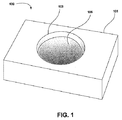
サセプタの構造に関して、図1を参照して、1つの態様によるサセプタ100の透視図を示した。サセプタ100は、本体101および基材を受容するための窪み103を含んでいる。図示したように、窪み103は円形の外形を有しており、そして1つの態様によれば、窪みは約5.0cm以上の直径を有している。他の態様によれば、窪み103の直径はより大きく、例えば約7.5cm以上、例えば約10cm以上である。好ましい態様では、円形の窪み103は、円形の外形および基材の配向のための平坦な部分を有することができる。理解できるように、基材は平板を含むことができ、それは結晶学的配向をあ表し、そしてそのように、窪み103は特別な結晶学的配向の基材を受容し、また配向させるための平板部を含むことができる。更に、サセプタ100は複数の窪みを含んでいてもよい。
Regarding the structure of the susceptor, referring to FIG. 1, a perspective view of a
窪み103は、基材を適切に保持するように設計された平均深さを有しており、そして1つの態様によれば、窪み103の深さは約800ミクロン以下である。他の態様では、窪み103の平均深さは約700ミクロン以下であり、更に約600ミクロン以下である。通常は、サセプタは加工されることが予期されるウエハの厚さに対応する窪み深さを有することができ、通常は300〜550ミクロンの水準、例えば約400ミクロンの窪み深さを有することができる。サセプタは、好ましくはウエハ厚さよりも僅かに小さい窪み深さを有することができる。
The
窪みは表面105を有しており、それは通常は窪みの底面であり、そしてこの態様によれば、該表面は平滑であり、また基材の均一な加熱を促進する。従って、1つの態様では、表面105は約8.0ミクロン以下の表面粗度Rmaxを有しており、例えば約5.0ミクロン以下、更に約2.0ミクロン以下である。更に、1つの好ましい態様では、表面105は約1.0ミクロン以下の表面粗度Rmaxを有している。
The recess has a
更にサセプタに関して、図2を参照して、1つの態様によるサセプタ200の一部の断面図が与えられる。前述のように、サセプタはケイ素を含浸させた炭化ケイ素材料を含んでいる。1つの態様によれば、サセプタ本体201の組成物は、約70質量%以上の炭化ケイ素を含み、例えば約80質量%以上の炭化ケイ素、更には約90質量%以上の炭化ケイ素を含んでいる。1つの好ましい態様では、サセプタ本体201は、約95質量%以上の炭化ケイ素を含んでいる。このように、サセプタ本体201はある量の含浸されたケイ素を含んでおり、好ましくは形成の間に炭化ケイ素中に含浸された金属ケイ素を有している。1つの態様によれば、サセプタ本体201は通常は、約30質量%以下の量のケイ素を含んでおり、例えば約15質量%以下、更に約10質量%以下の量のケイ素を含んでいる。好ましい態様では、サセプタ本体201は約5.0質量%以下のケイ素を含んでいる。
Further with respect to the susceptor, referring to FIG. 2, a cross-sectional view of a portion of a susceptor 200 according to one aspect is provided. As described above, the susceptor includes a silicon carbide material impregnated with silicon. According to one embodiment, the composition of the
ケイ素で構造を含浸することは、密度の増加をもたらし、またそのようなことで、サセプタの本体は通常は低度の気孔率を有し、これは主として密閉気孔率である。通常は、サセプタ本体201は約15容積%以下の気孔率、例えば約10容積%以下、更に約7.5容積%以下の気孔率を有している。通常は、気孔率は5容積%以下であり、例えば3容積%以下であり、更には1容積%以下である。
Impregnating the structure with silicon results in an increase in density, and as such, the body of the susceptor usually has a low porosity, which is primarily hermetic porosity. Usually, the
再度図2を参照すると、サセプタ200は更に本体を覆う窒化物層203を含んでいる。通常は、窒化物層203はサセプタ本体の外部表面を覆う材料の層であり、そして好ましくは窒化物層203は、さもなければ露呈する元素ケイ素を覆う材料の連続した膜であることができる。1つの態様によれば、窒化物層203は、サセプタ本体の外部表面積の約2.0%〜約20%の範囲を覆っている。
Referring again to FIG. 2, the susceptor 200 further includes a
図示したように、表面の不規則207、例えば元素ケイ素で充填された溝または小さな孔が、サセプタ本体201の中に存在していてもよく、また1つの態様によれば、窒化物層203がこれらの充填された表面不規則207を覆っている。より好ましくは、ケイ素が含浸された炭化ケイ素の場合には、以下でより詳細に議論されるように、サセプタの外部表面に露呈された元素ケイ素の部分だけが通常は窒化されている。1つの好ましい態様では、窒化物層203は、実質的に平滑な上部表面を維持しながら、このような不規則を覆っている。
As shown,
本体の表面に存在する可能性がある表面の不規則207のために、窒化物層203の厚さは平均厚さとして測定され、図2においては点線205で示されている。1つの態様によれば、窒化物層203の平均厚さは約0.2nm以上である。他の態様によれば、窒化物層203は約0.5nm以上の平均厚さを有することができ、更には約1.0nm以上、例えば約5.0nm以上の平均厚さを有することができる。好ましい態様によれば、窒化物層203は約0.5nm〜約2.0nmの範囲の平均厚さを有している。
Due to
通常は、窒化物層203は、約1000℃を越える温度に耐えることができるセラミックまたは金属を含んでいる。1つの好ましい態様では、窒化物層203はケイ素を含み、例えば窒化物層203の大部分は窒化ケイ素を含んでいる。1つの態様によれば、窒化物層203は約90質量%以上の窒化ケイ素を含んでおり、例えば約95質量%以上の窒化ケイ素、更には約98質量%以上の窒化ケイ素を含んでいる。更に、他の態様では、窒化物層203は本質的に窒化ケイ素である。
Typically, the
更に、窒化物層203は通常は密度の高い材料の層であり、低い有効率を有している。窒化物層203の有効率は、大部分は密閉有効率であるが、通常は約5.0容積%以下である。1つの態様によれば、窒化物層203の有効率は約2.0容積%以下、更には約1.0容積%以下である。
Further, the
ここに規定されたこのようなサセプタの形成に関して、米国特許第3951587号明細書に開示されている手順に従ったケイ素処理された炭化ケイ素本体の形成を行うことができ、その明細書は参照によって組み込まれる。サセプタ形状は明らかに幾つかのセラミック形成技術によって形成することができるが、1つの好ましい方法はスリップキャスト成形である。実質的にいずれの長さおよび直径、そしていずれの形状の複雑さのサセプタも、スリップキャスト成形によって、容易にまた経済的に達成される。他の適切な方法としては、プレス成形、例えば静水圧プレス成形、ホットプレス成形、または冷却圧縮成形、またはそれらの組み合わせが挙げられる。一度炭化ケイ素プリフォームが作られれば、熱処理が行われ、用いられる時間−温度条件に応じて、種々の度合いの再結晶の生起を伴った炭化ケイ素粒子の焼結をもたらす。 With respect to the formation of such a susceptor as defined herein, the formation of a siliconized silicon carbide body can be performed according to the procedure disclosed in US Pat. No. 3,951,587, the specification of which is hereby incorporated by reference. Incorporated. While the susceptor shape can obviously be formed by several ceramic forming techniques, one preferred method is slip casting. Susceptors of virtually any length and diameter and complexity of any shape are easily and economically achieved by slip casting. Other suitable methods include press molding, such as isostatic pressing, hot press molding, or cold compression molding, or combinations thereof. Once the silicon carbide preform is made, a heat treatment is performed, resulting in sintering of the silicon carbide particles with varying degrees of recrystallization occurring, depending on the time-temperature conditions used.
サセプタをそのように処理した後に、ケイ素を焼結した炭化ケイ素構造中へと導入するためにサセプタは次いで第二の熱処理に付されるが、それは焼結した部品を、約2150℃の温度で、減圧したもしくは少なくとも非酸化雰囲気で、約10分間ケイ素と接触させることによってなされる。このことは、焼結された形状の密度によって約5.0質量%から約30質量%までの量の金属ケイ素を、部分的にもしくは全体に含浸された焼結された形状をもたらす。この金属ケイ素は、通常は極めて純粋で、すなわち99%以上の純度、そして好ましくは99.9%の純粋なケイ素である。 After such treatment of the susceptor, the susceptor is then subjected to a second heat treatment to introduce silicon into the sintered silicon carbide structure, which causes the sintered part to be heated at a temperature of about 2150 ° C. By contacting with silicon for about 10 minutes in a vacuum or at least in a non-oxidizing atmosphere. This results in a sintered shape partially or wholly impregnated with metal silicon in an amount from about 5.0% to about 30% by weight depending on the density of the sintered shape. This metallic silicon is usually very pure, i.e. more than 99% pure and preferably 99.9% pure silicon.
他の方法では、上記の焼結工程は除かれ、そして焼成されていない成形品を直接に上記のようなケイ素処理(ケイ素含浸)工程に付される。この方法では、炭化ケイ素粒子は焼結され、そして基質(matrix)は含浸され、その全てが1つの工程で行われる。この方法が用いられても、または前者が用いられても、多孔質の炭化ケイ素の形状は、毛管現象および/または重力が含浸を促進するようにこの形状をケイ素と接触させるように配置することにより、または成形した物品を2150℃でケイ素蒸気に暴露することにより、浸漬によってケイ素で処理することができる。 In other methods, the sintering step described above is eliminated and the unfired molded article is directly subjected to a silicon treatment (silicon impregnation) step as described above. In this method, the silicon carbide particles are sintered and the matrix is impregnated, all in one step. Regardless of whether this method is used or the former is used, the shape of the porous silicon carbide is positioned so that the shape contacts the silicon so that capillary action and / or gravity promotes impregnation. Or by treating the molded article with silicon vapor at 2150 ° C. to treat with silicon.
ケイ素含浸処理および場合によっては機械加工工程の後に、ケイ素含浸された形状は窒化処理工程に付されて最終的なサセプタが形成される。この窒化処理工程はサセプタを窒素雰囲気中で加熱することを含むことができ、例えばサセプタは窒素含有雰囲気(例えば、窒素もしくはアンモニア)に、高温で暴露され、元素ケイ素または遊離のケイ素との直接反応によって窒化物層の形成をもたらし、好ましくは窒化ケイ素を形成する。通常の窒素種(例えば、窒素もしくはアンモニア)の分圧は約102Pa〜106Paの範囲である。 After the silicon impregnation process and possibly the machining process, the silicon-impregnated shape is subjected to a nitriding process to form the final susceptor. This nitriding step can include heating the susceptor in a nitrogen atmosphere, for example, the susceptor is exposed to a nitrogen-containing atmosphere (eg, nitrogen or ammonia) at an elevated temperature and directly reacted with elemental silicon or free silicon. Leads to the formation of a nitride layer, preferably to form silicon nitride. The partial pressure of a normal nitrogen species (eg, nitrogen or ammonia) is in the range of about 10 2 Pa to 10 6 Pa.
通常は、サセプタは約500℃超の温度、また通常は約800℃〜約1400℃の範囲に加熱される。このような温度範囲は、窒化物層の形成を促進し、またサセプタに機械的な歪をもたらす過剰な温度を回避させる。あるいは、この方法は物理的または化学的蒸気堆積の使用を含むことができる。図3の参照により、1つの態様によるLED形成の方法を示す工程系統図が与えられる。図示したように、第一の工程は窪みを有するサセプタの準備を含んでおり、この態様では301と記載されている。特に、サセプタは、ケイ素を含浸させた炭化ケイ素材料および本体を覆う窒化物層、を含む本体を有している。このサセプタは、雰囲気および温度制御を有する成長チャンバーの中で準備することができる。好ましくは、サセプタはMOCVDチャンバーの中で準備することができる。 Typically, the susceptor is heated to a temperature above about 500 ° C and usually in the range of about 800 ° C to about 1400 ° C. Such a temperature range facilitates formation of the nitride layer and avoids excessive temperatures that cause mechanical strain on the susceptor. Alternatively, the method can include the use of physical or chemical vapor deposition. With reference to FIG. 3, a process flow diagram is provided illustrating a method of LED formation according to one embodiment. As shown, the first step involves the preparation of a susceptor with a depression, which is described as 301 in this embodiment. In particular, the susceptor has a body including a silicon carbide material impregnated with silicon and a nitride layer covering the body. This susceptor can be prepared in a growth chamber with ambient and temperature control. Preferably, the susceptor can be prepared in a MOCVD chamber.
適切なサセプタ301を準備した後に、サセプタ103上に基材が配置される。この基材は、それに続く半導体層のエピタキシャル成長のための結晶成長表面を提供し、多層LED構造の形成を促進する。通常は、この基材は単結晶ウエハ材料であり、通常はボール(boule)または他のバルクの結晶形態から切出される。基材の材料としては、元素または合成物を挙げることができ、例えば炭化ケイ素、ケイ素、サファイア、アルミナ、窒化亜鉛もしくは窒化ガリウム(GaN)を挙げることができる。1つの態様では、基材の材料は単結晶ウエハであり、本質的に炭化ケイ素またはサファイアを含んでいる。他の態様によれば、基材はc−平面成長表面を有するサファイア基材であり、それはサファイア基材のc−平面が堆積に暴露されるようにサセプタ上に配置される。
After preparing the
基材はサセプタの表面上に配置することができる。サセプタは、ここでの態様に記載されるように窪みを含んでいることができ、またそうして、基材は、成長表面を暴露させて窪みの中に配置することができる。サセプタの中の窪みは、基材をサセプタ上に正確に配置することを容易にし、また従って堆積チャンバー中へ正確に配置することを容易にする。更に、幾つかの用途においては、基材は動かされるかまたは回転され、そして窪みが基材とサセプタの更なる結びつきを与える。 The substrate can be placed on the surface of the susceptor. The susceptor can include a depression as described in the embodiments herein, and so the substrate can be placed in the depression with the growth surface exposed. The depression in the susceptor facilitates accurate placement of the substrate on the susceptor and thus facilitates accurate placement in the deposition chamber. Further, in some applications, the substrate is moved or rotated and the indentation provides an additional bond between the substrate and the susceptor.
図3によれば、サセプタ303上に基材を供給した後に、基材305上に1つまたはそれ以上の下層が形成される。通常は、1つまたはそれ以上の下層は、それに続く半導体層の成長の適切な成長表面鋳型を提供するように形成することができる。このような下層としては、例えば、1つまたはそれ以上の緩衝層、膜、マスクもしくはパターン形成された層、または結晶質材料の非合体(non-coalescing)アイランドもしくはメサ(mesas)を挙げることができる。好ましくは、異質な基材上への半導体層成長の文脈の中では、下層(単数または複数)として、基材の成長表面の結晶学的構造よりも、覆っている半導体層の結晶学的構造により親密に適合する結晶学的構造を有する材料を挙げることができる。適切な材料としては、AlN、GaN、AlInN、GaAlN、Si、SiO2、ZnOまたはそれらの混合物を挙げることができる。1つの好ましい態様によれば、下層はAlNで作られた緩衝層である。
According to FIG. 3, one or more lower layers are formed on the
下層(単数または複数)は、堆積法によって形成することができ、例えばエピタキシャル成長法、所望によっては写真平版法を挙げることができる。1つの態様によれば、下層(単数または複数)はMOCVD(またはMOVPEとも称される)を用いて堆積される。更に、写真平版のパターン形成は、覆っている半導体層のエピタキシャルな横方向の成長(ELO)法を可能にするのに用いることができる。下層の形成は高温処理、例えば約800℃超の温度、または更に1000℃超の温度を用いることができる。あるいは、1つの好ましい態様では、下層は低温層、例えば約800℃未満の温度、例えば約600℃未満の温度で形成された層であることができる。 The lower layer (s) can be formed by a deposition method, for example, an epitaxial growth method or, if desired, a photolithographic method. According to one embodiment, the underlying layer (s) is deposited using MOCVD (or also referred to as MOVPE). Furthermore, photolithography patterning can be used to enable an epitaxial lateral growth (ELO) method of the overlying semiconductor layer. The formation of the lower layer can use high temperature processing, for example, temperatures above about 800 ° C., or even temperatures above 1000 ° C. Alternatively, in one preferred embodiment, the lower layer can be a low temperature layer, such as a layer formed at a temperature of less than about 800 ° C, such as a temperature of less than about 600 ° C.
上記の態様では、下層は通常はそれに続く半導体層の結晶成長の鋳型として提供され、また通常は半導体層に比べて極めて薄い。1つの態様によれば、下層は約400オングストローム未満の平均厚さを有し、例えば約300オングストローム未満であり、更に例えば約200オングストローム未満である。他の態様によれば、緩衝層は約50オングストローム〜約300オングストロームの範囲の平均厚さを有している。 In the above embodiment, the lower layer is usually provided as a template for crystal growth of the subsequent semiconductor layer, and is usually much thinner than the semiconductor layer. According to one aspect, the lower layer has an average thickness of less than about 400 angstroms, for example, less than about 300 angstroms, and for example, less than about 200 angstroms. According to another aspect, the buffer layer has an average thickness in the range of about 50 angstroms to about 300 angstroms.
再度図3を参照して、下層305の形成の後に、第一の半導体層を下層307を覆って形成することができる。通常は、第一の半導体層は発光領域の形成を促進する第一の層の1つである。第一の半導体層は、堆積法によって形成することができ、例えばエピタキシャル成長で形成することができる。1つの態様によれば、第一の半導体層は蒸気堆積法、例えばMOCVDまたはMOVPEによって形成される。通常は、形成処理は高温処理であり、また1つの態様によれば、第一の半導体層の成長は約500℃以上の温度、例えば約700℃以上、更には約900℃以上の温度で行われる。更に、1つの態様では、第一の半導体層は約1000℃以上の温度で形成される。
Referring again to FIG. 3, after forming the
更に第一の半導体層に関しては、他の態様によれば、第一の半導体層の形成は青色LED装置の形成に適した半導体層の形成を含んでいる。そのように、1つの態様では、第一の半導体層はIII族窒化物合成物を含んでいる。1つの態様では、第一の半導体層は、Ga、AlおよびInからなる元素の群からの少なくとも1種の元素を含んでいる。1つの好ましい態様では、第一の半導体層はGaNを含んでいる。 Further with respect to the first semiconductor layer, according to another aspect, forming the first semiconductor layer includes forming a semiconductor layer suitable for forming a blue LED device. As such, in one embodiment, the first semiconductor layer includes a Group III nitride composite. In one embodiment, the first semiconductor layer includes at least one element from the group of elements consisting of Ga, Al, and In. In one preferred embodiment, the first semiconductor layer includes GaN.
第一の半導体層の形成は、半導体材料へのドーパントの注入を含むことができ、例えばn型またはp型ドーパント材料の注入を含むことができる。1つの態様によれば、第一の半導体層の形成はn型ドーパントの材料への注入を含んでいる。通常は、ドーパントとして使用する濃度および元素は、ドープされる半導体材料の性質に依存する。1つの態様では、第一の半導体層はGaNを含んでおり、また第一の半導体層はドープされてn型の半導体層を形成する。好ましい態様では、第一の半導体層はGaNを含み、またn型半導体層は、GaN含有層の実質的な部分をドナー元素、例えばケイ素(Si)でドープすることによって形成される。従って、GaN層中のドナー濃度は、300Kで約1.0×1017cm-3以上であることができ、例えば約1.0×1018cm-3以上であることができる。 Formation of the first semiconductor layer can include implantation of a dopant into the semiconductor material, for example, implantation of an n-type or p-type dopant material. According to one embodiment, forming the first semiconductor layer includes implanting an n-type dopant into the material. Usually, the concentration and elements used as dopants depend on the nature of the semiconductor material to be doped. In one embodiment, the first semiconductor layer includes GaN and the first semiconductor layer is doped to form an n-type semiconductor layer. In a preferred embodiment, the first semiconductor layer includes GaN and the n-type semiconductor layer is formed by doping a substantial portion of the GaN-containing layer with a donor element, such as silicon (Si). Accordingly, the donor concentration in the GaN layer can be about 1.0 × 10 17 cm −3 or more at 300 K, for example, about 1.0 × 10 18 cm −3 or more.
場合によっては、層中のドーパントの活性化は意図的な処理工程を要求する。そのように、1つの態様によれば、ドープされた第一の半導体層を形成する方法はまた、ドーパントの活性化を含んでいる。このような方法は、特定の雰囲気での特定の温度での熱的なアニーリング、または電子線を用いた放射工程、例えば低エネルギー電子線放射(LEEBI)活性化、を含むことができる。 In some cases, activation of the dopant in the layer requires an intentional processing step. As such, according to one aspect, a method of forming a doped first semiconductor layer also includes dopant activation. Such a method can include thermal annealing at a specific temperature in a specific atmosphere, or a radiation step using an electron beam, for example, low energy electron beam radiation (LEEEBI) activation.
再度図3を参照すれば、本方法は更に、第一の半導体層309を覆う、第二の半導体層の形成を含んでいる。第一の半導体層と同様に、第二の半導体層は発光領域の形成を可能にする。第二の半導体層は堆積法、例えばエピタキシャル成長法、によって形成することができ、また1つの態様によれば、第二の半導体層は蒸気堆積法、例えばMOCVDまたはMOVPEによって形成される。他の態様によれば、第一の半導体層の形成は、約500℃以上の温度、例えば約700℃以上、更には約900℃以上の温度で行われる。更に、1つの態様では、第二の半導体層は約1000℃以上の温度で形成される。
Referring again to FIG. 3, the method further includes forming a second semiconductor layer that covers the
第二の半導体層の組成に関しては、他の態様によれば、第二の半導体層の形成は青色LED装置の形成に適した半導体層の形成を含んでいる。そのように、1つの態様では、第二の半導体層はIII族窒化物合成物を含んでいる。1つの態様では、第二の半導体層は、Ga、AlおよびInからなる元素の群からの少なくとも1種の元素を含んでいる。1つの好ましい態様では、第二の半導体層はGaNを含んでいる。 With regard to the composition of the second semiconductor layer, according to another aspect, the formation of the second semiconductor layer includes the formation of a semiconductor layer suitable for forming a blue LED device. As such, in one embodiment, the second semiconductor layer comprises a group III nitride composite. In one embodiment, the second semiconductor layer contains at least one element from the group of elements consisting of Ga, Al and In. In one preferred embodiment, the second semiconductor layer includes GaN.
更に第二の半導体層の形成に関しては、ドーパントを半導体材料へ注入することができる。上記の好ましい態様では、第一の半導体層がn型ドーパントを含んでいるので、第二の半導体層はp型ドーパントを含んでいる。好ましい態様によれば、第二の半導体層はGaNを含み、またp型層は、GaN、または少なくともGaNの実質的な部分を、マグネシウム(Mg)などの受容体元素でドーピングすることによって形成される。従って、GaN層中の受容体濃度は、通常は300Kで約1.0×1018cm-3以上であることができ、例えば300Kで約1.0×1019cm-3以上であることができる。第一の半導体層と関連して記載したように、第二の半導体層中にドープされた受容体を電気的に活性化するには意図的な活性化処理が要求される可能性がある。このような処理は特定の雰囲気での特定の温度での熱的なアニーリング、または放射処理を含むことができる。 Furthermore, for the formation of the second semiconductor layer, a dopant can be implanted into the semiconductor material. In said preferable aspect, since the 1st semiconductor layer contains the n-type dopant, the 2nd semiconductor layer contains the p-type dopant. According to a preferred embodiment, the second semiconductor layer comprises GaN and the p-type layer is formed by doping GaN or at least a substantial part of GaN with an acceptor element such as magnesium (Mg). The Therefore, the receptor concentration in the GaN layer can usually be about 1.0 × 10 18 cm −3 or more at 300K, for example, about 1.0 × 10 19 cm −3 or more at 300K. it can. As described in connection with the first semiconductor layer, an intentional activation process may be required to electrically activate the receptor doped in the second semiconductor layer. Such treatment can include thermal annealing at a particular temperature in a particular atmosphere, or radiation treatment.
一般に、ケイ素はドーパントとして用いることができるので、特にGaN構造のドーピングの文脈の中では、層の形成の間の形成チャンバー内における、追加の、もしくは未解明なケイ素の少量の存在でさえも、ドーパントとして機能し、装置の特性を実質的に変化させる可能性があると考えられている。このように、成長チャンバー内での、このような操作における使用には、ケイ素を含む成分は一般に望ましくなく、特に遊離のケイ素または金属ケイ素を含む成分は望ましくない。 In general, silicon can be used as a dopant, especially in the context of doping GaN structures, even in the presence of small amounts of additional or unresolved silicon in the formation chamber during layer formation. It is believed that it functions as a dopant and can substantially change the properties of the device. Thus, silicon-containing components are generally undesirable for use in such operations within the growth chamber, particularly those containing free silicon or metallic silicon.
図3に示した上記の方法は、1つの態様による、層状のLED構造の形成方法を与えることが理解されるであろう。通常は、1つまたはそれ以上の更なる層を、基材を覆って、第一と第二の半導体層の間に、形成することができる。1つの態様によれば、少なくとも1つの活性層を第一および第二の半導体層の間に形成することができる。 It will be appreciated that the above method illustrated in FIG. 3 provides a method of forming a layered LED structure according to one aspect. Typically, one or more additional layers can be formed between the first and second semiconductor layers over the substrate. According to one embodiment, at least one active layer can be formed between the first and second semiconductor layers.
前述のことに照らして、図4は、1つの態様による、層状のLED構造の説明を提供する。好ましくは、層状のLED構造は青色LED構造であり、これは一連の層を含んでおり、その中に基材401がある。上記のように、基材としては単結晶ウエハ材料が挙げられ、通常はボール(boule)または他のバルクの結晶形態から切出され、また通常は炭化ケイ素、ケイ素、サファイア、アルミナ、窒化亜鉛または窒化ガリウムなどの材料から作られる。好ましい態様によれば、基材の材料はサファイア、例えばc−平面成長表面を有するサファイア、の単結晶ウエハである。
In light of the foregoing, FIG. 4 provides an illustration of a layered LED structure according to one aspect. Preferably, the layered LED structure is a blue LED structure, which includes a series of layers in which a
図4を参照すれば、層状のLED構造はまた層403を含んでおり、これは通常は下層または緩衝層である。1つの態様によれば、層403は低温緩衝層であり、またMOCVDまたはMOVPEを用いて低温、通常は約500℃未満、で成長させることができる。1つの態様によれば、低温緩衝層は、薄く、約300オングストローム以下の厚さ、更には約200オングストローム以下の厚さを有している。更に、低温緩衝層は、Al、Ga、InおよびNなどの元素、またはそれらの組み合わせを含むことができる。好ましい態様では、緩衝層はAlNである。
Referring to FIG. 4, the layered LED structure also includes a
層403を覆っているのは層405であり、これは好ましい態様では半導体層である。好ましくは、青色LED構造の文脈では、層405はGaN半導体層である。より好ましくは、層405はn型GaN半導体層であり、これはケイ素がドープされている。このような態様では、ケイ素をドープしたGaN層は層403よりも厚く、約1.0ミクロン超の厚さ、通常は約1.0ミクロン〜約5.0ミクロンの範囲の厚さを有している。
Covering
更に図4を参照すると、層405を覆っているのは層407であり、これは1つの態様によれば活性層である。1つの態様によれば、この活性層は1つの材料層であり、例えば層405と411の間に二重ヘテロ接合構造を形成する層である。更に、他の態様では、層407は一連の層を含み、それらは単一量子井戸(SQW)構造または多重量子井戸(MQW)構造を含むことができる。1つの態様によれば、活性層はGa、AlおよびInなどの元素、またはそれらの組み合わせを含むことができる。活性層の特に適切な合成物としては、AlInGaN、AlGaN、InGaNおよびGaNが挙げられる。活性層が複数の層を含み量子井戸構造を形成する場合には、それぞれの層の厚さは薄く、例えば約100オングストローム以下、または約50オングストローム以下であることができ、また場合によっては、約25オングストローム以下であることができる。
Still referring to FIG. 4, covering
図4の層状のLED構造を参照すると、層407を覆っているのは層411であり、それは1つの態様によれば、他の半導体層である。好ましくは、層411はAlGaN半導体層であることができ、またより好ましくはマグネシウムをドープしたAlGaN層であることができる。そのような態様では、マグネシウムをドープしたGaN層は、約500オングストローム超の厚さ、例えば約750オングストローム超、更には約1000オングストローム超の厚さを有することができる。
Referring to the layered LED structure of FIG. 4, covering
層411を覆っているのは層413であり、これは1つの態様によれば、他の半導体層である。好ましくは、層413はGaN半導体層であることができ、またより好ましくは層413はマグネシウムをドープしたGaN層であることができる。そのような態様では、マグネシウムをドープしたGaN層は、約1000オングストローム超の厚さ、例えば約1500オングストローム超、更には約2000オングストローム超の厚さを有することができる。
Covering
図4は更に接点409と415を示しており、それらは1つの態様では、それぞれn型およびp型の接点である。通常は、III族窒化物種、例えばGaNを含む半導体層、の文脈の中では、n型の接点はコモンメタル、例えばAl、Ti、Inまたはそれらの組み合わせ、を含んでいる。p型接点は、通常はNi、Au、Pd、Ptなどの金属またはそれらの組み合わせを含んでいる。通常は、p型接点は透明または半透明であり、またそのように、通常は薄層であり、しばしば約400オングストロームまたはそれ未満の厚さを有している。
FIG. 4
個々に記載した態様によれば、サセプタおよびそのようなサセプタを用いたLED装置の形成方法は技術水準のサセプタを超えた改良を提供する。ここでの態様によるサセプタの製造は高度な精度および厳密な寸法公差で、費用効率が高い方法で行うことができる。更に、そのようなサセプタは、LEDの加工に用いると、高品質のLED装置の形成、少なくとも部分的には優れた組成によって、高温での寸法安定性、および寸法精度を可能とし、装置品質に悪影響を有する温度ムラを制御し、また最小化することができる。更に、サセプタ中の遊離ケイ素の量を低減させるという実用上の懸念にもかかわらず、ケイ素を含浸させた炭化窒素構造を有するここでの態様では、窒化処理を遊離ケイ素を結合するのに使用することによって遊離ケイ素の含量を制御する。更に、いずれかの態様による、ここに記載された特徴の組み合わせを有するサセプタはまた、LED装置の製造、著しく改善された青色LED装置の製造に役立つ。 According to the individually described aspects, susceptors and methods of forming LED devices using such susceptors provide improvements over state-of-the-art susceptors. The manufacture of the susceptor according to this embodiment can be performed in a cost-effective manner with a high degree of precision and tight dimensional tolerances. In addition, such susceptors, when used in LED processing, enable high-quality LED devices, at least partially superior composition, enabling dimensional stability and dimensional accuracy at high temperatures, resulting in improved device quality. Temperature irregularities with adverse effects can be controlled and minimized. Furthermore, in this embodiment having a nitrogen carbide structure impregnated with silicon, despite the practical concern of reducing the amount of free silicon in the susceptor, nitriding is used to bond the free silicon. Thereby controlling the free silicon content. Furthermore, a susceptor having a combination of features described herein according to any aspect is also useful in the manufacture of LED devices, significantly improved blue LED devices.
本発明を特定の態様の文脈の中で説明し、また記載してきたが、開示した詳細に限定することを意図したものではない。何故なら、種々の変更および置換を、本発明の範囲からの何らかの逸脱なしに行うことができるからである。例えば、追加のもしくは等価の代替物を準備することが可能であり、また追加のもしくは等価の製造工程を用いることが可能である。このように、ここに開示した本発明の更なる変更および等価物を、単なる日常の実験を用いることによって当業者がなし得る可能性があり、そしてこのような全ての変更および等価物は以下の特許請求の範囲によって記載した本発明の範囲に入ると信じられる。 Although the invention has been described and described in the context of specific embodiments, it is not intended to be limited to the details disclosed. This is because various changes and substitutions can be made without any deviation from the scope of the present invention. For example, additional or equivalent alternatives can be provided, and additional or equivalent manufacturing processes can be used. Thus, further modifications and equivalents of the invention disclosed herein may be made by those of ordinary skill in the art using only routine experimentation, and all such modifications and equivalents are described below. It is believed that it will fall within the scope of the invention as set forth in the claims.
本発明により、高品質のLED装置を形成する方法、およびLED装置の製造に特に適切なサセプタが提供される。 The present invention provides a method of forming a high quality LED device and a susceptor that is particularly suitable for the manufacture of LED devices.
Claims (20)
(i)単結晶ウエハを受容するための窪みを有するサセプタ本体であって、該窪みが約10ミクロン以下の表面粗度Rmaxを有する表面を有しており、またケイ素が含浸された炭化ケイ素を含むサセプタ本体、および
(ii)該サセプタ本体を覆っている窒化物層、を含むサセプタを準備すること、
基材をサセプタ本体の窪みの中に配置すること(該基材は成長表面を有している)、
該成長表面を覆う第一の半導体層を形成すること、および
第一の半導体層を覆う第二の半導体層を形成すること(発光領域が第一の半導体層および第二の半導体層の間に形成される)、を含む方法。 A method for forming a semiconductor LED device, comprising:
(I) A susceptor body having a recess for receiving a single crystal wafer, the recess having a surface having a surface roughness R max of about 10 microns or less, and silicon carbide impregnated with silicon Providing a susceptor comprising: a susceptor body comprising: (ii) a nitride layer covering the susceptor body;
Placing the substrate in a recess in the susceptor body (the substrate has a growth surface);
Forming a first semiconductor layer covering the growth surface, and forming a second semiconductor layer covering the first semiconductor layer (a light emitting region between the first semiconductor layer and the second semiconductor layer); Formed).
炭化ケイ素を含む多孔質のプリフォームを準備すること、
多孔質のパーフォームに元素シリコンを含浸させてサセプタ本体を形成すること、
サセプタ本体を覆う窒化物層を形成すること(サセプタ本体は単結晶ウエハを受容するための窪みを有しており、該窪みは約10ミクロン以下の表面粗度Rmaxを有する表面を有している)、を含む方法。 A method of forming a susceptor,
Providing a porous preform comprising silicon carbide;
Impregnating a porous perform with elemental silicon to form a susceptor body;
Forming a nitride layer overlying the susceptor body (susceptor body has a recess for receiving a single-crystal wafer, depressions body is has a surface having the surface roughness R max of about 10 microns Including).
Applications Claiming Priority (2)
| Application Number | Priority Date | Filing Date | Title |
|---|---|---|---|
| US86522106P | 2006-11-10 | 2006-11-10 | |
| PCT/US2007/084261 WO2008058270A2 (en) | 2006-11-10 | 2007-11-09 | A susceptor and method of forming a led device using such susceptor |
Publications (1)
| Publication Number | Publication Date |
|---|---|
| JP2010509778A true JP2010509778A (en) | 2010-03-25 |
Family
ID=39324157
Family Applications (1)
| Application Number | Title | Priority Date | Filing Date |
|---|---|---|---|
| JP2009536510A Pending JP2010509778A (en) | 2006-11-10 | 2007-11-09 | Susceptor and method for forming LED device using susceptor |
Country Status (6)
| Country | Link |
|---|---|
| US (1) | US20080110402A1 (en) |
| EP (1) | EP2080221B1 (en) |
| JP (1) | JP2010509778A (en) |
| CN (1) | CN101563771A (en) |
| AT (1) | ATE513311T1 (en) |
| WO (1) | WO2008058270A2 (en) |
Families Citing this family (3)
| Publication number | Priority date | Publication date | Assignee | Title |
|---|---|---|---|---|
| KR20120101633A (en) * | 2009-10-14 | 2012-09-14 | 아사히 가라스 가부시키가이샤 | Jig for semiconductor production and method for producing same |
| US20140256082A1 (en) * | 2013-03-07 | 2014-09-11 | Jehad A. Abushama | Method and apparatus for the formation of copper-indiumgallium selenide thin films using three dimensional selective rf and microwave rapid thermal processing |
| US10490437B2 (en) * | 2015-04-07 | 2019-11-26 | Sumco Corporation | Susceptor, vapor deposition apparatus, vapor deposition method and epitaxial silicon wafer |
Citations (5)
| Publication number | Priority date | Publication date | Assignee | Title |
|---|---|---|---|---|
| JPS5366164A (en) * | 1976-11-26 | 1978-06-13 | Hitachi Ltd | Susceptor for semiconductor wafer processing |
| JPH0758041A (en) * | 1993-08-20 | 1995-03-03 | Toshiba Ceramics Co Ltd | Susceptor |
| JP2003197535A (en) * | 2001-12-21 | 2003-07-11 | Sumitomo Mitsubishi Silicon Corp | Vapor growth device, method for detecting temperature of vapor growth device, and method for controlling temperature of vapor growth device |
| JP2004088077A (en) * | 2002-06-28 | 2004-03-18 | Toshiba Ceramics Co Ltd | Member for processing semiconductor wafer |
| JP2005255440A (en) * | 2004-03-10 | 2005-09-22 | Univ Meijo | Method for making group iii nitride semiconductor and group iii nitride semiconductor |
Family Cites Families (18)
| Publication number | Priority date | Publication date | Assignee | Title |
|---|---|---|---|---|
| US3951587A (en) * | 1974-12-06 | 1976-04-20 | Norton Company | Silicon carbide diffusion furnace components |
| US4795673A (en) * | 1978-01-09 | 1989-01-03 | Stemcor Corporation | Composite material of discontinuous silicon carbide particles and continuous silicon matrix and method of producing same |
| US4633051A (en) * | 1983-11-23 | 1986-12-30 | Advanced Semiconductor Materials America, Inc. | Stable conductive elements for direct exposure to reactive environments |
| JPS6169116A (en) * | 1984-09-13 | 1986-04-09 | Toshiba Ceramics Co Ltd | Susceptor for continuous cvd coating on silicon wafer |
| JPS6447019A (en) * | 1987-08-18 | 1989-02-21 | Denki Kagaku Kogyo Kk | Glassy carbon coated susceptor |
| JPH06287091A (en) * | 1993-02-02 | 1994-10-11 | Ngk Insulators Ltd | Sic-containing far-infrared ray emitter, drier and firing unit |
| US5837058A (en) * | 1996-07-12 | 1998-11-17 | Applied Materials, Inc. | High temperature susceptor |
| JPH10233529A (en) * | 1997-02-14 | 1998-09-02 | Hewlett Packard Co <Hp> | Nitride semiconductor element and its manufacture |
| US6026589A (en) * | 1998-02-02 | 2000-02-22 | Silicon Valley Group, Thermal Systems Llc | Wafer carrier and semiconductor apparatus for processing a semiconductor substrate |
| US6162543A (en) * | 1998-12-11 | 2000-12-19 | Saint-Gobain Industrial Ceramics, Inc. | High purity siliconized silicon carbide having high thermal shock resistance |
| US6673198B1 (en) * | 1999-12-22 | 2004-01-06 | Lam Research Corporation | Semiconductor processing equipment having improved process drift control |
| US6960743B2 (en) * | 2000-12-05 | 2005-11-01 | Ibiden Co., Ltd. | Ceramic substrate for semiconductor manufacturing, and method of manufacturing the ceramic substrate |
| US7394043B2 (en) * | 2002-04-24 | 2008-07-01 | Sumitomo Electric Industries, Ltd. | Ceramic susceptor |
| US7255775B2 (en) * | 2002-06-28 | 2007-08-14 | Toshiba Ceramics Co., Ltd. | Semiconductor wafer treatment member |
| US7256375B2 (en) * | 2002-08-30 | 2007-08-14 | Asm International N.V. | Susceptor plate for high temperature heat treatment |
| US7582166B2 (en) * | 2003-08-01 | 2009-09-01 | Sgl Carbon, Llc | Holder for supporting wafers during semiconductor manufacture |
| US20060060145A1 (en) * | 2004-09-17 | 2006-03-23 | Van Den Berg Jannes R | Susceptor with surface roughness for high temperature substrate processing |
| US7632609B2 (en) * | 2005-10-24 | 2009-12-15 | Shin-Etsu Chemical Co., Ltd. | Fabrication method of photomask-blank |
-
2007
- 2007-11-09 JP JP2009536510A patent/JP2010509778A/en active Pending
- 2007-11-09 US US11/938,085 patent/US20080110402A1/en not_active Abandoned
- 2007-11-09 EP EP07868710A patent/EP2080221B1/en not_active Not-in-force
- 2007-11-09 CN CNA200780041923XA patent/CN101563771A/en active Pending
- 2007-11-09 AT AT07868710T patent/ATE513311T1/en not_active IP Right Cessation
- 2007-11-09 WO PCT/US2007/084261 patent/WO2008058270A2/en active Application Filing
Patent Citations (5)
| Publication number | Priority date | Publication date | Assignee | Title |
|---|---|---|---|---|
| JPS5366164A (en) * | 1976-11-26 | 1978-06-13 | Hitachi Ltd | Susceptor for semiconductor wafer processing |
| JPH0758041A (en) * | 1993-08-20 | 1995-03-03 | Toshiba Ceramics Co Ltd | Susceptor |
| JP2003197535A (en) * | 2001-12-21 | 2003-07-11 | Sumitomo Mitsubishi Silicon Corp | Vapor growth device, method for detecting temperature of vapor growth device, and method for controlling temperature of vapor growth device |
| JP2004088077A (en) * | 2002-06-28 | 2004-03-18 | Toshiba Ceramics Co Ltd | Member for processing semiconductor wafer |
| JP2005255440A (en) * | 2004-03-10 | 2005-09-22 | Univ Meijo | Method for making group iii nitride semiconductor and group iii nitride semiconductor |
Also Published As
| Publication number | Publication date |
|---|---|
| US20080110402A1 (en) | 2008-05-15 |
| ATE513311T1 (en) | 2011-07-15 |
| WO2008058270A3 (en) | 2008-07-10 |
| EP2080221B1 (en) | 2011-06-15 |
| WO2008058270A2 (en) | 2008-05-15 |
| EP2080221A2 (en) | 2009-07-22 |
| CN101563771A (en) | 2009-10-21 |
Similar Documents
| Publication | Publication Date | Title |
|---|---|---|
| JP4677065B2 (en) | Light emitting diode and manufacturing method thereof | |
| JP5371430B2 (en) | Semiconductor substrate, method for manufacturing a self-supporting semiconductor substrate by hydride vapor phase epitaxy, and mask layer used therefor | |
| TWI502770B (en) | A method for manufacturing a nitride semiconductor device, a nitride semiconductor light emitting device, and a light emitting device | |
| CN102414796B (en) | Method for fabricating wafer products and method for fabricating gallium nitride semiconductor photonic elements | |
| CN101061571B (en) | Semiconductor multilayer substrate, method for producing same and light-emitting device | |
| JP2006290676A (en) | Group iii-v nitride semiconductor substrate and method for manufacturing the same | |
| TW201133919A (en) | Epitaxial formation structures and associated methods of manufacturing solid state lighting devices | |
| TW200931586A (en) | Fabrication apparatus and fabrication method of semiconductor device produced by heating substrate | |
| TWI252599B (en) | N-type group III nitride semiconductor layered structure | |
| TW201131806A (en) | Epitaxial formation support structures and associated methods | |
| CN104900773B (en) | A kind of nitride light-emitting diode structure and preparation method thereof | |
| CN105633223B (en) | Semiconductor devices in AlGaN templates, the preparation method of AlGaN templates and AlGaN templates | |
| TW511301B (en) | Method of heat-treating nitride compound semiconductor layer and method of producing semiconductor device | |
| JP2008034444A (en) | Group iii nitride semiconductor light emitting device, method of manufacturing same, and lamp | |
| JP3954335B2 (en) | Group III nitride multilayer film | |
| TW200527717A (en) | Method for manufacturing p-type group III nitride semiconductor, and group III nitride semiconductor light-emitting device | |
| JPH11135889A (en) | Substrate for crystal growth and light-emitting device using the same | |
| JP2010509778A (en) | Susceptor and method for forming LED device using susceptor | |
| WO2019123763A1 (en) | Method for producing group iii nitride semiconductor substrate | |
| JPH08186332A (en) | Manufacture of semiconductor element | |
| JP2009516377A (en) | Method for manufacturing a high quality semiconductor light emitting device on a silicon substrate | |
| TWI246208B (en) | Group III nitride semiconductor device and light-emitting device using the same | |
| CN103918061A (en) | Crystal layered structure and method for manufacturing same, and semiconductor element | |
| JP2008501234A (en) | Light emitting diode | |
| JP2005210091A (en) | Group iii nitride semiconductor element and light emitting element |
Legal Events
| Date | Code | Title | Description |
|---|---|---|---|
| A977 | Report on retrieval |
Free format text: JAPANESE INTERMEDIATE CODE: A971007 Effective date: 20110708 |
|
| A131 | Notification of reasons for refusal |
Free format text: JAPANESE INTERMEDIATE CODE: A131 Effective date: 20110802 |
|
| A601 | Written request for extension of time |
Free format text: JAPANESE INTERMEDIATE CODE: A601 Effective date: 20111101 |
|
| A602 | Written permission of extension of time |
Free format text: JAPANESE INTERMEDIATE CODE: A602 Effective date: 20111109 |
|
| A02 | Decision of refusal |
Free format text: JAPANESE INTERMEDIATE CODE: A02 Effective date: 20120403 |