JP2010197352A - Defect inspection method and defect inspecting apparatus - Google Patents
Defect inspection method and defect inspecting apparatus Download PDFInfo
- Publication number
- JP2010197352A JP2010197352A JP2009045857A JP2009045857A JP2010197352A JP 2010197352 A JP2010197352 A JP 2010197352A JP 2009045857 A JP2009045857 A JP 2009045857A JP 2009045857 A JP2009045857 A JP 2009045857A JP 2010197352 A JP2010197352 A JP 2010197352A
- Authority
- JP
- Japan
- Prior art keywords
- scattered light
- wafer
- defect
- defect inspection
- detection
- Prior art date
- Legal status (The legal status is an assumption and is not a legal conclusion. Google has not performed a legal analysis and makes no representation as to the accuracy of the status listed.)
- Pending
Links
Images


Classifications
-
- G—PHYSICS
- G01—MEASURING; TESTING
- G01N—INVESTIGATING OR ANALYSING MATERIALS BY DETERMINING THEIR CHEMICAL OR PHYSICAL PROPERTIES
- G01N21/00—Investigating or analysing materials by the use of optical means, i.e. using sub-millimetre waves, infrared, visible or ultraviolet light
- G01N21/84—Systems specially adapted for particular applications
- G01N21/88—Investigating the presence of flaws or contamination
- G01N21/95—Investigating the presence of flaws or contamination characterised by the material or shape of the object to be examined
- G01N21/9501—Semiconductor wafers
-
- G—PHYSICS
- G01—MEASURING; TESTING
- G01N—INVESTIGATING OR ANALYSING MATERIALS BY DETERMINING THEIR CHEMICAL OR PHYSICAL PROPERTIES
- G01N21/00—Investigating or analysing materials by the use of optical means, i.e. using sub-millimetre waves, infrared, visible or ultraviolet light
- G01N21/84—Systems specially adapted for particular applications
- G01N21/88—Investigating the presence of flaws or contamination
- G01N21/8806—Specially adapted optical and illumination features
-
- H—ELECTRICITY
- H01—ELECTRIC ELEMENTS
- H01L—SEMICONDUCTOR DEVICES NOT COVERED BY CLASS H10
- H01L22/00—Testing or measuring during manufacture or treatment; Reliability measurements, i.e. testing of parts without further processing to modify the parts as such; Structural arrangements therefor
- H01L22/10—Measuring as part of the manufacturing process
- H01L22/12—Measuring as part of the manufacturing process for structural parameters, e.g. thickness, line width, refractive index, temperature, warp, bond strength, defects, optical inspection, electrical measurement of structural dimensions, metallurgic measurement of diffusions
-
- G—PHYSICS
- G01—MEASURING; TESTING
- G01N—INVESTIGATING OR ANALYSING MATERIALS BY DETERMINING THEIR CHEMICAL OR PHYSICAL PROPERTIES
- G01N21/00—Investigating or analysing materials by the use of optical means, i.e. using sub-millimetre waves, infrared, visible or ultraviolet light
- G01N21/84—Systems specially adapted for particular applications
- G01N21/88—Investigating the presence of flaws or contamination
- G01N21/8806—Specially adapted optical and illumination features
- G01N2021/8809—Adjustment for highlighting flaws
-
- G—PHYSICS
- G01—MEASURING; TESTING
- G01N—INVESTIGATING OR ANALYSING MATERIALS BY DETERMINING THEIR CHEMICAL OR PHYSICAL PROPERTIES
- G01N21/00—Investigating or analysing materials by the use of optical means, i.e. using sub-millimetre waves, infrared, visible or ultraviolet light
- G01N21/84—Systems specially adapted for particular applications
- G01N21/88—Investigating the presence of flaws or contamination
- G01N21/8806—Specially adapted optical and illumination features
- G01N2021/8848—Polarisation of light
Landscapes
- Engineering & Computer Science (AREA)
- General Physics & Mathematics (AREA)
- Life Sciences & Earth Sciences (AREA)
- Pathology (AREA)
- Immunology (AREA)
- Analytical Chemistry (AREA)
- Health & Medical Sciences (AREA)
- General Health & Medical Sciences (AREA)
- Chemical & Material Sciences (AREA)
- Physics & Mathematics (AREA)
- Biochemistry (AREA)
- Manufacturing & Machinery (AREA)
- Computer Hardware Design (AREA)
- Power Engineering (AREA)
- Microelectronics & Electronic Packaging (AREA)
- Investigating Materials By The Use Of Optical Means Adapted For Particular Applications (AREA)
- Testing Or Measuring Of Semiconductors Or The Like (AREA)
Abstract
Description
本発明は、欠陥検査方法及び欠陥検査装置に係り、例えば、試料表面に存在する微小な欠陥を高感度かつ高速に検査する表面欠陥検査方法および検査装置に関する。 The present invention relates to a defect inspection method and a defect inspection apparatus, for example, a surface defect inspection method and an inspection apparatus for inspecting a minute defect existing on a sample surface with high sensitivity and high speed.
半導体基板や薄膜基板等の製造ラインにおいて、製品の歩留まりを維持・向上するために、半導体基板や薄膜基板等の表面に存在する欠陥の検査が行われている。従来技術としては特開平9-304289号公報(特許文献1)、特開2000-162141号公報(特許文献2)が知られている。微小な欠陥を検出するために試料表面上に数十μmに集光したレーザビームを照射して、欠陥からの散乱光を集光・検出し、数十nmから数μm以上の寸法の欠陥を検出している。 In a production line for semiconductor substrates, thin film substrates, and the like, in order to maintain and improve product yield, inspection of defects existing on the surface of semiconductor substrates, thin film substrates, and the like is performed. As prior arts, JP-A-9-304289 (Patent Document 1) and JP-A 2000-162141 (Patent Document 2) are known. In order to detect minute defects, a laser beam focused to several tens of μm is irradiated on the sample surface to collect and detect scattered light from the defects, and defects with dimensions of several tens to several μm or more are detected. Detected.
半導体の微細化に伴い、要求される欠陥検出感度も微細化の一途を辿っており、散乱光の偏光検出などの感度向上手法が用いられてきた(特許文献3)。偏光検出を行うことで、レーザ照射部の試料表面荒れから発生する散乱光(以後ラフネス散乱光と表記)を選択的に抑制可能となり、検出感度を向上させることは可能である。
また近年では、欠陥検出感度以外にも試料表面荒れの状態をモニタリングするニーズも高まっている。試料表面荒れはラフネス散乱光の大きさに基づき算出され、Haze(ヘイズ)信号と呼ばれる。Haze信号をモニタリングすることで、プロセス管理を行っている(非特許文献1)。
Along with the miniaturization of semiconductors, the required defect detection sensitivity continues to be miniaturized, and a technique for improving sensitivity such as polarization detection of scattered light has been used (Patent Document 3). By performing polarization detection, it is possible to selectively suppress scattered light (hereinafter referred to as roughness scattered light) generated from the sample surface roughness of the laser irradiation unit, and it is possible to improve detection sensitivity.
In recent years, in addition to the defect detection sensitivity, there is an increasing need for monitoring the state of sample surface roughness. The sample surface roughness is calculated based on the magnitude of the roughness scattered light, and is called a Haze signal. Process management is performed by monitoring the Haze signal (Non-Patent Document 1).
近年LSI配線は急激に微細化しており、検出すべき欠陥のサイズは光学式検査の検出限界に近づいている。半導体ロードマップによると2012年には36nmノードのLSIの量産が開始されようとしており、DRAMハーフピッチの程度の大きさを有する欠陥を検出する能力が必要とされている。欠陥とはウエハ上に付着するパーティクルや結晶欠陥COP(Crystal Originated Particle)、研磨により生じるスクラッチなどである。 In recent years, LSI wiring has been rapidly miniaturized, and the size of defects to be detected is approaching the detection limit of optical inspection. According to the semiconductor roadmap, mass production of 36nm node LSI is about to start in 2012, and the ability to detect defects with the size of DRAM half pitch is required. Defects include particles adhering to the wafer, crystal defects COP (Crystal Originated Particles), scratches caused by polishing, and the like.
欠陥に対してレーザで照明を行った時に発生する散乱光の大きさIは、欠陥の粒径をdとすると、I∝d^6の関係があることが知られている。つまり欠陥サイズが小さくなると発生する散乱光は急速に減少するため、微細欠陥から発生する散乱光を増大させる必要がある。
発生する散乱光を大きくする方法として、レーザの高出力化が存在するが、上記手法では被照射部の温度が上昇し、試料にダメージを与える恐れがある。
It is known that the magnitude I of scattered light generated when a defect is illuminated with a laser has a relationship of I∝d ^ 6 where d is the particle size of the defect. That is, since the scattered light generated rapidly decreases as the defect size decreases, it is necessary to increase the scattered light generated from the fine defect.
As a method of increasing the generated scattered light, there is an increase in the output of the laser. However, in the above method, the temperature of the irradiated portion is increased, and there is a risk of damaging the sample.
試料表面の温度上昇を抑えて検出感度を向上させる手法として、偏光検出が有効であることは上述したが、偏光検出とHaze計測の両立は困難である。検査装置では、検出した散乱光を電気信号に変換し、その電気信号に対し周波数帯域で分離を行っており、高周波成分を欠陥信号、低周波成分をHaze信号として処理している。つまり偏光検出により、ラフネス散乱光を抑制することで、Haze信号が大幅に低減されることになり、Haze計測の精度や安定性が低下する恐れがある。 As described above, polarization detection is effective as a technique for improving detection sensitivity by suppressing a temperature rise on the sample surface, but it is difficult to achieve both polarization detection and Haze measurement. The inspection apparatus converts the detected scattered light into an electrical signal, separates the electrical signal in a frequency band, and processes the high frequency component as a defect signal and the low frequency component as a Haze signal. That is, by suppressing the roughness scattered light by polarization detection, the Haze signal is greatly reduced, and there is a possibility that the accuracy and stability of the Haze measurement may be lowered.
以上のことより、(1)ウエハへのダメージを抑制すること、(2)偏光検出を利用した欠陥検出感度向上とHaze計測を両立させること、上記二点が課題となる。
本発明は、試料へのダメージを抑えつつ、偏光検出を利用した欠陥検出感度向上とHaze計測を両立させる検査方法および装置を提供することを目的とする。
From the above, (1) suppressing damage to the wafer, (2) improving both defect detection sensitivity using polarization detection and Haze measurement, the above two points are problems.
SUMMARY OF THE INVENTION An object of the present invention is to provide an inspection method and apparatus that can simultaneously improve defect detection sensitivity using polarization detection and Haze measurement while suppressing damage to a sample.
上記課題を解決すべく、本発明は試料に対し、エネルギの吸収が小さい波長帯域を有するレーザビームを発振する光源と、前記光源から発振されたレーザビーム照射により、欠陥から発生する欠陥散乱光を検出する欠陥検出光学系と、ウエハ表面荒れから発生するラフネス散乱光を検出するHaze検出光学系の二つを独立に備え、前記二つの検出光学系で検出した散乱光に対し独立に偏光検出を行い、前記二つの異なる検出信号に基づき欠陥判定および、Haze計測を行うことを特徴とする。ここで、エネルギの吸収が小さいということは、ウエハに照射されたエネルギがウエハ表面の極近傍のみで吸収されず、ウエハ内部までエネルギが浸透する状態を示す。 In order to solve the above-described problems, the present invention is directed to a light source that oscillates a laser beam having a wavelength band in which energy absorption is small with respect to a sample, and defect scattered light generated from a defect by irradiation of the laser beam emitted from the light source. It has two independent detection systems, a defect detection optical system and a Haze detection optical system that detects roughness scattered light generated from the rough surface of the wafer, and polarization detection is independent of the scattered light detected by the two detection optical systems. And performing defect determination and Haze measurement based on the two different detection signals. Here, the fact that the energy absorption is small indicates that the energy irradiated to the wafer is not absorbed only in the immediate vicinity of the wafer surface, and the energy penetrates to the inside of the wafer.
また、前記照明波長は405nm・488nm・532nmのいずれかであることを特徴とする。 Further, the illumination wavelength is any one of 405 nm, 488 nm, and 532 nm.
また、ウエハ被照射領域から発生した散乱光はハーフミラー・PBS(Polarized Beam Splitter)・ダイクロイックミラーなどで、振幅分離・偏光分離・波長分離された後に、欠陥検出光学系とHaze検出光学系で検出されることを特徴とする。 Scattered light generated from the irradiated area of the wafer is detected by the defect detection optical system and the Haze detection optical system after amplitude separation, polarization separation, and wavelength separation by half mirror, PBS (Polarized Beam Splitter), dichroic mirror, etc. It is characterized by being.
前記二つの異なる検出系において、独立検出を行うために振幅分離が用いられた場合には、透過率の異なる複数のハーフミラーを切り替えることで、欠陥検出光学系とHaze検出光学系の検出散乱光量を調節可能とすることを特徴とする。 When amplitude separation is used to perform independent detection in the two different detection systems, the amount of scattered light detected by the defect detection optical system and the Haze detection optical system can be switched by switching a plurality of half mirrors having different transmittances. Can be adjusted.
前記二つの検出系において、独立検出を行うために波長分離が用いられた場合には、二つの異なる波長を発振する光源を有し、一方の波長による照明で発生した散乱光を欠陥検出光学系で検出し、他方の波長による照明で発生した散乱光をHaze検出光学系で検出することを特徴とする。 When wavelength separation is used to perform independent detection in the two detection systems, the defect detection optical system has a light source that oscillates two different wavelengths, and detects scattered light generated by illumination with one wavelength. And scattered light generated by illumination with the other wavelength is detected by a Haze detection optical system.
また、一つの検出光学系を有し、信号分離機を用いて欠陥信号とHaze信号を時間的に分離検出することで、欠陥信号とHaze信号を独立検出可能とすることを特徴とする。これにより、振幅分離・偏光分離・波長分離は必要ない。 In addition, it has one detection optical system, and the defect signal and the Haze signal can be detected independently by temporally separating and detecting the defect signal and the Haze signal using a signal separator. This eliminates the need for amplitude separation, polarization separation, and wavelength separation.
また、前記偏光検出における透過偏光軸は、ユーザが検査する膜種を入力し、その膜種とデータベースと比較することで、偏光軸を設定可能であることを特徴とする。ここでデータベースとは、膜種毎に変化する欠陥散乱光とラフネス散乱光の偏光状態を事前にシミュレーションにより計算し、欠陥・Hazeそれぞれの検出感度を最大化する検出条件を準備したデータの集合である。 The transmission polarization axis in the polarization detection is characterized in that a polarization axis can be set by inputting a film type to be inspected by a user and comparing the film type with a database. Here, the database is a set of data that prepares detection conditions that maximize the detection sensitivity of each defect and Haze by calculating the polarization states of the defect scattered light and roughness scattered light that change for each film type by simulation in advance. is there.
本発明によれば、ウエハ表面の上昇温度を抑制しつつ照射エネルギを増大させ、かつ偏光検出による感度向上とHaze計測とを両立可能とする欠陥検査方法及び装置を提供することができる。 According to the present invention, it is possible to provide a defect inspection method and apparatus capable of increasing the irradiation energy while suppressing the rising temperature of the wafer surface, and making it possible to achieve both sensitivity improvement by polarization detection and Haze measurement.
以下に、図面を用いて実施例を詳細に説明する。 Hereinafter, embodiments will be described in detail with reference to the drawings.
本発明の実施例の一例を図1で説明する。図1は概略、照明光学系101、検出光学系102、ウエハステージ103および回路・信号処理部から構成される。該照明光学系101はレーザ光源2、ビームエキスパンダ3、偏光素子4、ミラーm、集光レンズ6より構成される。レーザ光源2から射出されたレーザビーム200はビームエキスパンダ3でビーム径を所望の大きさに調整され、偏光素子4で所望の偏光状態へ変換され、反射ミラーmを介し、集光レンズ6でウエハ1の被検査領域に照明を行う。
An example of the embodiment of the present invention will be described with reference to FIG. 1 schematically includes an illumination
レーザ光源2としては、ウエハ1の表面極近傍(表面から100nm以下の深さ)に存在する欠陥の検出には、試料内部に浸透しにくい紫外、真空紫外のレーザビームを発振し、試料内部(表面から100nm以上の深さ)の欠陥の検出には試料内部に浸透しやすい可視、赤外のレーザビームを発振するする光源が用いられる。
As a
ビームエキスパンダ3はアナモフィック光学系であり、複数のプリズムから構成される。光軸に互いに垂直な平面内における一方向のみに関してビーム径を変化させ、集光レンズ6を使ってウエハ1にスポット照明、または線状照明を行う。集光レンズ6とビームエキスパンダ3の組合せでなくても、シリンドリカルレンズを用いて線状照明を行っても構わない。シリンドリカルレンズ単体を用いた場合はアナモフィック光学系を用いて光軸に互いに垂直な平面内における一方向のみにビーム径を変化させずとも、ウエハ上に線状照明を行うことが可能となるため、ビームエキスパンダ3を省略可能となり、光学系のスリム化が図れる点で有効である。
The
該検出光学系102は、欠陥検出光学系102aとHaze検出光学系102bから構成される。ウエハ1におけるレーザ照射部から発生した散乱光は検出レンズ8で集光され、ビームスプリッタ9にて2つの光路に分割され、分割された該散乱光は集光レンズ10a、10b、およびフィルタ11a、11bを介し、光電子増倍管12a、12bで検出される。
該ビームスプリッタ9は、例えばハーフミラーやPBSであり、ウエハ1上におけるレーザ照射部から発生し、検出レンズ8で集光された散乱光に対し、振幅分離、または偏光分離を行うことで、欠陥検出光学系102aとHaze検出光学系102bにて、独立に散乱光を検出可能とする。
The detection
The
該フィルタ11aと11bは偏光板や液晶であり、検出する偏光軸を調節可能である。ウエハに照射されるレーザビーム200が、ある偏光特性を有していた場合には、そのレーザ照射により欠陥から発生する散乱光や、ラフネスから発生する散乱光はそれぞれ特定の偏光状態を有しており、前記偏光状態は照明条件と検出条件に依存して変化する。散乱光の偏光状態はシミュレーションにより計算可能であり、照明条件・検出条件毎に欠陥散乱光のみを透過、またはカットしやすい偏光軸や、ラフネス散乱光のみを透過、またはカットしやすい偏光軸を把握することは可能である。つまり、フィルタ11aは欠陥散乱光のみを通過させやすい偏光軸に調整し、フィルタ11bはラフネス散乱光のみを通過させやすい偏光軸に調整することで、欠陥検出光学系102aでは、欠陥から発生した散乱光のみを高い感度で検出可能となり、Haze検出光学系102bでは、ラフネス散乱光のみを高い感度で検出することが可能となる。
The
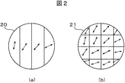
該フィルタ11a・11bは図2に示すように、複数のセグメントに分割され、それぞれが異なる偏光軸を有していても構わない。図2(a)では1次元的に偏光軸が変化しているフィルタ20の一例を、図2(b)では2次元的に偏光軸が変化しているフィルタ21の一例を示している。また、該セグメントの分割数や分割の仕方、また偏光軸の方向にも制限はない。
該ビームスプリッタ9は、複数の異なる透過率を有するスプリッタを保持し、これを変更することにより、欠陥検出光学系とHaze検出光学系の感度を調節可能である。例えば、欠陥検出光学系102aへの透過率を50%、Haze検出光学系102bへの反射率を50%と設定し、欠陥検出感度が必要な感度に達していない場合には、欠陥検出光学系102aへの透過率を90%、Haze検出光学系102bへの反射率を10%に変更することで、欠陥検出光学系で検出可能な散乱光が大きくなるため、欠陥検出感度を向上させることが可能となる。
As shown in FIG. 2, the
The
該光電子増倍管12a、12bは散乱光を受光し光電変換するために用いられるものであり、TVカメラ、CCDカメラ、フォトダイオードやリニアセンサ、あるいはイメージインテンシファイアをこれらと組み合わせた高感度なイメージセンサ、あるいはマルチアノード光電子増倍管などを使用しても構わない。例えば二次元センサを用いることで、広い領域を一度に検査することが可能となる。
The
該光電子増倍管12a、12bは受光光量に応じた電気信号を発生させ、該電気信号はアナログ回路150に導かれる。アナログ回路150で行われる処理に関して以下、説明する。
レーザ照射により、被照射部からは図3のような信号が検出される。表面荒れから発生するラフネス散乱光N0はレーザ照射期間中は常に発生しており、低周波なうねりとして検出される(<数kHz)。ラフネス散乱光N0が光電子増倍管に入射し光電変換される時に、ランダムな変動であるショットノイズn0が発生し、これも同時に検出される。一方、欠陥から発生する欠陥散乱光S0は、幅数十μm程度のビームが欠陥の存在する位置を通過する間の時間だけ、パルス状に発生するため、ラフネス散乱光と比較して高周波である(>数kHz)。つまり図3記載の検出信号がアナログ回路に導かれてきた際には、前記検出信号に対し、ハイパスフィルタを適用することで欠陥信号を抽出でき、ローパスフィルタを適用することでHaze信号を抽出可能となる。
The
A signal as shown in FIG. 3 is detected from the irradiated portion by laser irradiation. Roughness scattered light N 0 generated from surface roughness is always generated during the laser irradiation period and is detected as low-frequency swell (<several kHz). When the roughness scattered light N 0 enters the photomultiplier tube and undergoes photoelectric conversion, a shot noise n 0 that is a random fluctuation is generated, and this is also detected at the same time. On the other hand, the defect scattered light S 0 generated from the defect is generated in a pulse shape only during the time during which the beam having a width of about several tens of μm passes through the position where the defect exists. Yes (> several kHz). That is, when the detection signal shown in FIG. 3 is introduced to an analog circuit, a defect signal can be extracted by applying a high-pass filter to the detection signal, and a Haze signal can be extracted by applying a low-pass filter. It becomes.
以上のことより、光電子増倍管12aで検出した欠陥散乱光に基づき発生した電気信号に対してはハイパスフィルタがかけられ、光電子増倍管12bで検出したラフネス散乱光に基づき発生した電気信号に対してはローパスフィルタがかけられる。アナログ回路150では、さらに信号増幅、アナログ−デジタル変換を施される。前記検出信号に基づき、信号処理部151では閾値処理による欠陥判定、およびレベル判定によるHaze処理が行われ、CPU152を介して、マップ出力部153で図4記載の欠陥マップ160およびHazeマップ161を表示する。欠陥マップ160は検査時に取り込んだ欠陥信号と座標を基に表示され、Hazeマップ161は検査時に取り込んだHaze信号と座標を基に表示される。また入力部154にはユーザインターフェースを含み、ユーザがレシピ設定などを行う。
From the above, the high-pass filter is applied to the electric signal generated based on the defect scattered light detected by the
該ウエハステージ103はウエハ1を保持するチャックおよび高さ制御を行うZステージ(図示せず)、ウエハを回転させるための回転ステージ14およびウエハを半径方向に移動させるための併進ステージ15から構成される。該ウエハステージ103は回転走査および併進走査を行うことによって、レーザビーム照射位置がウエハ全面を螺旋状に照明するように走査を行う。また所望の領域を照明できるように、ステージ制御部155で回転速度、併進速度を制御する。
The
図1では照明光学系101、検出光学系102が1つずつある例で説明を行ったが、ウエハに対して低い仰角θlから照明を行う斜方照明光学系、ウエハに対し概略垂直方向から照明を行う垂直照明光学系、またウエハに対し低い仰角θsで検出を行う低角度検出光学系、ウエハに対し前記低角度検出光学系より高い仰角で検出を行う高角度検出光学系のように照明光学系、検出光学系が複数仰角方向に存在しても構わない(図示せず)。
Figure 1 In the illumination
ウエハ上に付着するパーティクルに対しては、斜方照明光学系で照明を行った場合は、垂直照明光学系よりも異物に対する散乱断面積を大きくすることができるため、欠陥から発生する散乱光量が大きくなり、感度向上に効果がある。また数十nmの大きさの欠陥からの散乱光は低仰角側に強く散乱し、百nm以上の大きさの欠陥からの散乱光は高仰角側に強く散乱するため、微細な欠陥は低仰角検出光学系で検出し、比較的大きな欠陥は高仰角検出光学系で検出することで、検出可能な欠陥サイズのレンジを大きくすることが可能となる。 For particles adhering to the wafer, when the oblique illumination optical system is used to illuminate, the scattering cross-sectional area for foreign matter can be made larger than that of the vertical illumination optical system. It becomes large and is effective in improving sensitivity. In addition, scattered light from defects with a size of several tens of nm is strongly scattered on the low elevation angle side, and scattered light from defects with a size of 100 nm or more is strongly scattered on the high elevation angle side. By detecting with a detection optical system and detecting a relatively large defect with a high elevation angle detection optical system, it is possible to increase the range of defect sizes that can be detected.
一方、COPやスクラッチのようなウエハに対する凹み欠陥には、垂直照明光学系で照明を行ったほうが、散乱断面積が大きくなるため、凹み欠陥に対する感度を向上させることが可能となる。また凹み欠陥からの散乱光は高仰角側に強く散乱するため、高仰角検出光学系を用いることで、さらに検出感度を向上させることが可能となる。
上記説明のように、欠陥の種類(パーティクル、COP、スクラッチなど)や大きさに応じて、欠陥から発生する散乱光の強度分布や仰角特性が変化するため、照明方向・検出方向毎の信号を組み合わせて比較することで、欠陥分類精度や欠陥寸法算出精度を向上させることが可能となる。
On the other hand, when a dent defect on a wafer such as COP or scratch is illuminated with a vertical illumination optical system, the scattering cross section becomes larger, and therefore the sensitivity to the dent defect can be improved. Moreover, since the scattered light from the dent defect is strongly scattered toward the high elevation angle side, the detection sensitivity can be further improved by using the high elevation angle detection optical system.
As described above, the intensity distribution and elevation angle characteristics of the scattered light generated from the defect change according to the type (particle, COP, scratch, etc.) and size of the defect. By combining and comparing, it is possible to improve defect classification accuracy and defect size calculation accuracy.
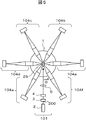
図5は図1に示す実施例の平面図の一例である。図5のように異なる方位角方向φに複数の検出光学系が存在しても構わない。ウエハ1、照明光学系101、検出光学系104a〜104f、照明スポット25を示している。検出光学系104a〜104fはそれぞれ欠陥検出光学系102aとHaze検出光学系102bで構成される。検出信号はアナログ回路150で増幅、ノイズ除去処理、アナログ−デジタル変換を施され、検出光学系104a〜104fにて概略同一領域が照明されている時に発生した散乱光信号同士を加算し、信号処理部151では該加算された信号に基づき欠陥判定およびHaze判定処理が行われ、CPU152を介してマップ出力部153で欠陥マップ160およびHazeマップ161を表示する。
FIG. 5 is an example of a plan view of the embodiment shown in FIG. As shown in FIG. 5, a plurality of detection optical systems may exist in different azimuth angle directions φ. A
以上、複数方位角方向に検出光学系が存在する実施例を説明したが、複数方位角に検出光学系が存在することの利点として、使用する検出光学系を選択、または各検出における検出信号に重み付けをして使用することにより、欠陥検出感度を向上させることができる点がある。ラフネス散乱光は、ウエハ表面の粗さ状態に依存して、方位角依存性が存在する。例えば、Siのように表面粗さが非常にスムースなウエハでは、レーザビーム200が入射してきた方向、つまり検出光学系104e・104fが存在する方位角方向にラフネス散乱光が強く発生する傾向があり、Alデポ膜のように表面粗さが大きいウエハでは、レーザビーム200が進行していく方向、つまり検出光学系104b・104cが存在する方位角方向にラフネス散乱光が強く発生する性質がある。ラフネス散乱光が弱く発生する方位角に存在する欠陥検出光学系で検出された検出信号のみを用いる、またはラフネス散乱光の大きさに応じた重みをゲインとして検出信号に乗算して、処理することにより、欠陥検出感度を向上させることが可能となる。
As described above, the embodiments in which the detection optical systems exist in a plurality of azimuth directions have been described. However, as an advantage of the presence of the detection optical systems in a plurality of azimuth angles, a detection optical system to be used is selected or a detection signal for each detection is used. There is a point that the defect detection sensitivity can be improved by using the weight. The roughness scattered light depends on the azimuth angle depending on the roughness of the wafer surface. For example, a wafer with a very smooth surface, such as Si, has a tendency to generate intensely scattered scattered light in the direction in which the
検出光学系の配置について、図5では異なる方位角方向に6個の検出光学系を配置している例を挙げたが、検出光学系の個数は6個である必要はなく、配置する方位角方向に制限もない。また、概略同じ仰角θsに複数の検出光学系が配置されている必要もない。さらに概略同じ方位角に検出器が配置されている必要もない。 Regarding the arrangement of the detection optical systems, FIG. 5 shows an example in which six detection optical systems are arranged in different azimuth angle directions, but the number of detection optical systems does not have to be six, and the azimuth angles to be arranged are arranged. There are no restrictions on the direction. Further, it is not necessary to arrange a plurality of detection optical systems at substantially the same elevation angle θs. Furthermore, it is not necessary that the detectors are arranged at substantially the same azimuth angle.
図5では照明の長手方向と平行な方向からレーザ照明を行っているが、照明の長手方向とレーザを照射する方向は概略同じである必要はなく、異なる方向から照明を行っても構わない。異なる方向から照明する利点として、スクラッチなど欠陥形状に方向性を有する欠陥の分類性能を向上させることができる点がある。COPなど、方位角方向に対して概略対称である欠陥から発生する散乱光には方位角依存性が存在せず、全方位角方向に概略均等に発生する。一方、スクラッチなどのように方位角方向に対して対象でない欠陥から発生する散乱光には方位角依存性が存在する。またスクラッチからの散乱光の方位角特性は照明の入射する方位角にも依存するため、照明方向を能動的に変化させ、各方位角方向に存在する検出系の信号を比較することで、欠陥分類精度や寸法算出精度を向上させることが可能となる。 In FIG. 5, laser illumination is performed from a direction parallel to the longitudinal direction of illumination, but the longitudinal direction of illumination and the direction of irradiating the laser need not be substantially the same, and illumination may be performed from different directions. As an advantage of illuminating from different directions, there is a point that it is possible to improve the classification performance of defects such as scratches having directionality in the defect shape. Scattered light generated from a defect that is substantially symmetric with respect to the azimuth direction, such as COP, has no azimuth dependency and is generated almost uniformly in all azimuth directions. On the other hand, scattered light generated from defects that are not targeted with respect to the azimuth angle direction such as scratches has azimuth angle dependency. In addition, since the azimuth angle characteristics of the scattered light from the scratch depend on the azimuth angle where the illumination is incident, it is possible to actively change the illumination direction and compare the detection system signals present in each azimuth angle direction. It is possible to improve classification accuracy and size calculation accuracy.
複数方位角、複数仰角方向にある各検出器信号の処理方法に関して、各検出信に対して加算、または平均化処理が行われる。加算することにより、検出光量が大きくなるため、検出感度向上に効果があり、平均化することにより、センサのダイナミックレンジ内で検出可能なサイズの幅が増えることになり、ダイナミックレンジ拡大に効果がある。 Regarding the processing method of each detector signal in a plurality of azimuth angles and a plurality of elevation angle directions, addition or averaging processing is performed on each detection signal. Addition increases the amount of light detected, which is effective in improving detection sensitivity, and averaging increases the range of sizes that can be detected within the dynamic range of the sensor, which is effective in expanding the dynamic range. is there.
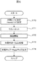
次に、欠陥検出処理フローについて、図6を用いて説明する。まずレシピ設定で照明方向・照射エネルギ・センサ感度などの検査条件を設定する。欠陥検出レシピだけでなく、Haze計測レシピの設定もこれに含まれる(ステップ170)。ウエハをステージにセットし(ステップ171)、検査を開始する(ステップ172)。検出信号に基づいて欠陥判定を行い(ステップ173)、欠陥マップとHazeマップを表示する(ステップ174)。 Next, the defect detection processing flow will be described with reference to FIG. First, inspection conditions such as illumination direction, irradiation energy, and sensor sensitivity are set in the recipe setting. This includes not only the defect detection recipe but also the setting of the Haze measurement recipe (step 170). The wafer is set on the stage (step 171), and inspection is started (step 172). Defect determination is performed based on the detection signal (step 173), and a defect map and a Haze map are displayed (step 174).
本発明の第二の実施例を図7で説明する。図7は概略、照明光学系101、検出光学系102、ウエハステージ103および回路・信号処理部から構成される。
該照明光学系101はλ1のレーザビームを発振する光源2aを有する照明光学系101aとλ1とは異なる波長λ2のレーザビームを発振する光源2bを有する照明光学系101bから構成される。それぞれの光源から発振されたレーザビーム200a、200bはビームエキスパンダ3a・3bでビーム径を所望の大きさに調整され、偏光素子4a・4bにて所望の偏光状態へ変換され、ミラーmを介し、集光レンズ6a・6bでウエハ1の概略同一領域へ照射される。
該ビームスプリッタ9は、第二の実施例においてはダイクロイックミラーなど、波長分離を行う素子を用いればよい。波長がλ1であるレーザビーム200aで照明され、欠陥より発生した欠陥散乱光を欠陥検出光学系102aで検出し、波長がλ2であるレーザビーム200bで照明され、表面荒れより発生したラフネス散乱光をHaze検出光学系102bで検出する。
A second embodiment of the present invention will be described with reference to FIG. 7 schematically includes an illumination
The illumination
The
以下、2つの異なる波長で欠陥散乱光とラフネス散乱光を独立に検出する利点に関して説明する。
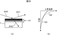
図8(a)はウエハ1にレーザビーム200が照射された際の、ウエハ1の内部に照射エネルギが吸収される様子を模式的に示している。ウエハ1に照明を行うと、照射エネルギの一部は反射し201、残りのエネルギは透過光202としてウエハ1内部に侵入する。該侵入したエネルギ202はウエハ1の内部へ侵入するにつれ、徐々に熱としてウエハ1に吸収される。ここで、前記透過光202のエネルギが(1/e)2まで減衰した時に侵入した距離d 31を浸透深度と呼ぶ。浸透深度が小さければ、エネルギは表層のみで吸収され、浸透深度が大きければ、エネルギはウエハ1内部まで侵入することになる。
Hereinafter, the advantage of independently detecting defect scattered light and roughness scattered light at two different wavelengths will be described.
FIG. 8A schematically shows how the irradiation energy is absorbed inside the
図8(b)は浸透深度が異なる二つの材質を対照とした場合の、深さ方向と上昇温度の関係を示している。曲線32は浸透深度が小さい材質の一例であり、ウエハ1表面近傍でエネルギが吸収されるため、ウエハ1表面での上昇温度が大きくなることを示している。曲線33は浸透深度が大きい材質の一例であり、ウエハ1内部までエネルギが侵入するため、ウエハ1表面での温度上昇は抑えることができる。つまり曲線32と曲線33の特性を示す材質に、概略同一のエネルギを照射した場合、曲線32の特性を示す材質のほうがウエハ1表面での上昇温度は大きくなる。浸透深度は物質や照明波長に応じて変化する。
欠陥検出感度向上のためには照射エネルギの増大は有効な手法であり、上記浸透深度に関する説明より、照射エネルギを増大させるためには、ウエハに対する浸透深度が大きい波長を光源として用い、レーザ照射を行えばよいことがわかる。
Siウエハを対象に波長355nmと波長532nmで照明を行う場合を一例として説明する。Siに波長355nmで照明を行った場合は、浸透深度は約10nmであるのに対し、532nmで照明を行った場合の浸透深度は約2μmである。つまり浸透深度の観点より、波長532nmで照明を行ったほうが上昇温度を抑えつつ、照射エネルギを増大させることが可能となるのは明白である。
FIG. 8B shows the relationship between the depth direction and the rising temperature when two materials having different penetration depths are used as controls. A curve 32 is an example of a material having a small depth of penetration, and shows that the temperature rise on the surface of the
Increasing the irradiation energy is an effective method for improving the defect detection sensitivity. From the above description of the penetration depth, in order to increase the irradiation energy, a wavelength with a large penetration depth to the wafer is used as a light source, and laser irradiation is performed. You can see that
A case where illumination is performed on a Si wafer at a wavelength of 355 nm and a wavelength of 532 nm will be described as an example. When Si is illuminated at a wavelength of 355 nm, the penetration depth is about 10 nm, whereas when penetration is performed at 532 nm, the penetration depth is about 2 μm. In other words, from the viewpoint of the penetration depth, it is obvious that the irradiation energy can be increased while suppressing the rising temperature when illumination is performed at a wavelength of 532 nm.
次にHaze計測と浸透深度の関係に関して説明する。
Haze計測のためには、概略表面荒れから発生するラフネス散乱光のみを検出することが望ましい。浸透深度が大きい波長で照明を行った場合、サンプル内部に存在するCOPから発生する散乱光も検出する可能性があり、Haze計測の精度や安定性が低下する恐れがある。つまりHaze計測の精度向上や安定性を確保するためには、ウエハに対する浸透深度が小さい波長で照明を行い、概略表面荒れから発生するラフネス散乱光のみを検出することが望ましいと言える。
Next, the relationship between Haze measurement and penetration depth will be described.
For Haze measurement, it is desirable to detect only roughness scattered light generated from rough surface roughness. When illumination is performed at a wavelength with a large penetration depth, there is a possibility that scattered light generated from the COP existing inside the sample may be detected, which may reduce the accuracy and stability of Haze measurement. In other words, in order to ensure the accuracy improvement and stability of Haze measurement, it is desirable to illuminate at a wavelength with a small penetration depth with respect to the wafer and detect only roughness scattered light generated from rough surface roughness.
以上のことより、パーティクルの検出感度を向上させるためには浸透深度の大きい波長で照明を行い、Haze計測の精度・安定性向上のためには浸透深度の小さい波長で照明を行えばよいことがわかる。
Siに対し浸透深度の大きい波長としては、例えば405nm・488nm・532nmなどであり、浸透深度の小さい波長としては、例えば355nm・266nmなどである。
From the above, in order to improve the detection sensitivity of particles, it is necessary to illuminate at a wavelength with a large penetration depth, and to improve the accuracy and stability of Haze measurement, it is necessary to illuminate at a wavelength with a small penetration depth. Recognize.
Wavelengths having a large penetration depth with respect to Si are, for example, 405 nm, 488 nm, and 532 nm, and wavelengths having a small penetration depth are, for example, 355 nm and 266 nm.
図7では照明光学系101aの入射仰角θ1と照明光学系101bのウエハへの入射仰角θ2が異なっている例で説明を行ったが、前記2つの入射仰角に制約はない。また前記2つのレーザビームの入射方位角に関しても、制約はない。
In FIG. 7, an example in which the incident elevation angle θ1 of the illumination
また、検出光学系102が1つの例で説明を行ったが、検出光学系が複数あっても構わない。また該複数の検出光学系の検出仰角や検出方位角にも制約はない。
Further, the detection
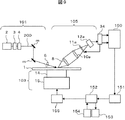
本発明の第三の実施例を図9で説明する。図9は概略、照明光学系101、検出光学系105、ウエハステージ103および回路・信号処理部から構成される。
該検出光学系105は、検出レンズ8、集光レンズ10a、フィルタ11aから構成され、散乱光を光電子増倍管12aで検出する。
該フィルタ11aは偏光板や液晶であり、欠陥散乱光のみを通過させやすい偏光軸に設定されている。後述するが、フィルタ11aは信号分離器34と同期して、偏光軸の回転、またはフィルタリングの有無を切り替え可能な構成である。
信号分離器34ではゲート回路のON/OFFの切り替えにより、光電子増倍管12aの検出信号を任意のタイミングで欠陥信号とHaze信号の2つの経路に切り替えることにより、分離検出する。
A third embodiment of the present invention will be described with reference to FIG. 9 schematically includes an illumination
The detection
The
The
信号分離機での切り替えタイミングを図10で説明する。図10はウエハに照射された照明スポット25が回転ステージ走査によりウエハ上を移動している様子と、信号処理部における欠陥信号とHaze信号とのゲート回路切り替えのタイミングの関係を表している。R軸は併進15ステージの進行方向であり、θ軸は回転ステージ14の回転方向を意味している。照明スポット25が存在している領域の面積は数十μm2程度であり、直径300mmのウエハの面積に対し、極微小な領域であるため、R軸とθ軸が概略直行する説明図で問題ない。線速vで回転しており、照明スポットの短手方向の長さ35を通過するのにT:(t1−t0)の時間を要している。t0を基準に考え、Δt(<T)の間だけ、ゲート回路切り替えにより、検出信号を欠陥信号として処理し、(T−Δt)の間だけゲート回路切り替えにより、検出信号をHaze信号として処理する。その後も、t1、t2、t3からΔtの間だけ欠陥信号として、(T−Δt)の間だけHaze信号として処理する。ここで、Δtの大きさは、数百ns〜数μsの間の時間である。上記タイミングでゲート回路を切り替えることで、非検査領域を作ることなく、一つの検出系で欠陥検出光学系とHaze検出光学系の効果を再現することが可能となる。検出光学系を削減可能となるため、コスト低減・実装スペースの縮小が可能となる。
The switching timing in the signal separator will be described with reference to FIG. FIG. 10 shows the relationship between the
前記フィルタ11aは、欠陥散乱光のみを通過させやすい偏光軸を有しているため、Haze信号取得時には表面ラフネスからの散乱光が大きくカットされる。信号分離器34が検出信号をHaze信号として処理している間は、ゲート回路切り替えタイミングに同期して、サーボモータなどによりフィルタ11aの偏光軸を回転させ、表面ラフネスからの散乱光のみを通過させやすい偏光状態に設定する。またHaze信号取得時にはフィルタリングを行わずに、偏光検出を行わなくても構わない。
Δtの時間を長くすれば、欠陥検出信号は大きく、Haze検出信号は小さくなり、逆にΔtの時間を短くすれば、欠陥検出信号は小さくなり、Haze検出信号は大きくなる。Δtの時間を調節することで、欠陥検出信号とHaze検出信号の大きさを調節可能である。
Since the
If the time of Δt is lengthened, the defect detection signal becomes large and the Haze detection signal becomes small. Conversely, if the time of Δt is shortened, the defect detection signal becomes small and the Haze detection signal becomes large. The magnitudes of the defect detection signal and the Haze detection signal can be adjusted by adjusting the time Δt.
PMT12aは受光光量に応じた電気信号を発生させ、その電気信号は信号分離器34により、欠陥検出信号とHaze検出信号に分離され、それぞれがアナログ回路150で必要な増幅、ノイズ除去処理、アナログ−デジタル変換を施され、信号処理部151で欠陥判定およびHaze判定処理が行われ、CPU152を介して、マップ出力部153で欠陥マップ160およびHazeマップ161を表示する。
検出光学系105が1つの例で説明を行ったが、検出光学系が複数あっても構わない。また該複数の検出光学系の検出仰角や検出方位角にも制約はない。
The
The detection
本発明の第四の実施例を図11で説明する。図11は概略、照明光学系101、検出光学系106、ウエハステージ103および回路・信号処理部から構成される。該照明光学系101はレーザ光源2、ビームエキスパンダ3、偏光素子4、ミラーm、集光レンズ6より構成される。レーザ光源2から射出されたレーザビーム200はビームエキスパンダ3でビーム径を所望の大きさに調整され、偏光素子4で所望の偏光状態へ変換され、集光レンズ6でウエハ1の被検査領域に線状照明を行う。
A fourth embodiment of the present invention will be described with reference to FIG. FIG. 11 schematically includes an illumination
ビームエキスパンダ3はアナモフィック光学系であり、複数のプリズムから構成される。光軸に互いに垂直な平面内における一方向のみに関してビーム径を変化させ、集光レンズ6を使ってウエハ1にスポット照明、または線状照明を行う。集光レンズ6とビームエキスパンダ3の組合せでなくても、シリンドリカルレンズを用いて線状照明を行っても構わない。シリンドリカルレンズ単体を用いた場合はアナモフィック光学系を用いて光軸に互いに垂直な平面内における一方向のみにビーム径を変化させずとも、ウエハ上に線状照明を行うことが可能となるため、ビームエキスパンダ3を省略可能となり、光学系のスリム化が図れる点で有効である。
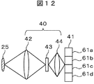
検出光学系106は、結像光学系40と、フォトダイオードアレイ41から構成される。該検出光学系106を詳細に示したものを図12に示す。検出光学系106は集光レンズ42、イメージインテンシファイア43、結像レンズ44およびフォトダイオードアレイ41で構成され、照明スポット25から散乱される光を集光レンズ42で集光し、イメージインテンシファイア43で散乱光を増幅させ、結像レンズ44を介してフォトダイオードアレイ41に結像する。フォトダイオードは画素61a〜61dを有する。
The
The detection
このフォトダイオードアレイ41は受光光量に応じた電気信号を発生させ、該電気信号はアナログ回路150で増幅、ノイズ除去処理、アナログ−デジタル変換を施され、信号処理部151で欠陥判定およびHaze判定処理が行われ、CPU152を介して、マップ出力部153で欠陥マップ160およびHazeマップ161を表示する。また入力部154ではユーザがレシピ設定を行う。
The
該ウエハステージ103はウエハ1を保持するチャックおよび高さ制御を行うZステージ(図示せず)、ウエハを回転させるための回転ステージ14およびウエハを半径方向に移動させるための併進ステージ15から構成される。該ウエハステージ103は回転走査および併進走査を行うことによって、レーザビーム照射位置がウエハ全面を螺旋状に照明するように走査を行う。また所望の領域を照明できるように、ステージ制御部155で回転速度、併進速度を制御する。
The
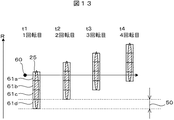
ステージは回転しながら半径方向(R方向)に概略一定速度で併進しており、概略一回転した時点で半径方向に進む距離を送りピッチと呼ぶ。回転・併進を行うことで照明スポットがウエハ全面を螺旋状に移動するように走査するのだが、照明スポット25の半径方向への長さは送りピッチに対し概略同じであり、一つの欠陥に対して一度しか照明を行わないことが多い。
The stage translates at a substantially constant speed in the radial direction (R direction) while rotating, and the distance traveled in the radial direction at the time of approximately one revolution is called the feed pitch. By rotating and translating, the illumination spot scans so that it moves spirally over the entire wafer surface. However, the length of the
本発明では線状照明を行い、照明スポット25の半径方向への長さを送りピッチの大きさより長くすることで同一欠陥に対して複数回照明を行うことを特徴としており、その検査方法に関して説明を行う。
In the present invention, linear illumination is performed, and the length of the
図13は照明スポット25の半径方向への長さが送りピッチ50の4倍の長さであり、欠陥60に対し4回照明を行う場合の説明図であり、これを用いて複数回照明の説明を行う。時刻t1に欠陥60に対し照明スポット25により一回目の照明を行い、欠陥から発生する散乱光は画素61aで検出される。時刻t2でウエハが概略一回転し、照明スポット25は概略送りピッチ50の距離だけ半径方向に進み、欠陥60を再度照明し、欠陥からの散乱光は画素61bで検出される。以後時刻t3、時刻t4でウエハが概略一回転し、欠陥60に対し照明を行い、それぞれ画素61c、画素61dで検出される。以上、図13の場合では欠陥60を4回照明することができ、該検出された複数の散乱光はアナログ回路または信号処理部で加算処理、または平均化処理を行われる。なお、照明回数は4回である必要はなく、複数回照明であれば何回でも構わない。加算回数を増加させることで、欠陥からの散乱光信号を増幅可能であるため、検出感度を向上できる。
またフォトダイオード41の画素数は4つである必要はない。
FIG. 13 is an explanatory diagram of the case where the length of the
The number of pixels of the
信号処理部での加算処理方法に関して、図14を用いて説明する。本発明においては、ウエハが1周する毎に概略同一領域を検出している画素が1つずつシフトしていくと捉えることができるため、検出信号を蓄積するメモリを1周する毎にシフトさせる。1回転目には画素61aの信号をメモリ65に蓄積し、それ以降は2回転目には画素61bの信号を、3回転目には画素61cの信号を、4回転目には画素61dの信号をメモリ65に蓄積する。これにより、概略同一領域の信号を加算することが可能になる。
以上、本実施例では検出光学系106が1つの例で説明を行ったが、検出光学系が複数あっても構わない。また該複数の検出光学系の検出仰角や検出方位角にも制約はない。
The addition processing method in the signal processing unit will be described with reference to FIG. In the present invention, it can be understood that the pixels detecting the substantially same region are shifted one by one every time the wafer goes around, so that the memory for storing the detection signal is shifted every time it goes around. . In the first rotation, the signal of the
In the present embodiment, the detection
また、イメージインテンシファイア43は、散乱光を増幅して微弱な散乱光を検出可能にする目的で使用しているが、イメージインテンシファイアを使わずとも例えばEM-CCDやマルチアノード光電子増倍管などのセンサ自体が高い増幅率を有するものを使用しても構わない。これらを用いた場合、検出光学系を小さいスペースに実装可能となるため、装置のスリム化が図れる点で有効である。
また、フォトダイオードアレイ41は、散乱光を受光し光電変換するために用いるものであり、TVカメラ、CCDカメラ、フォトダイオードやリニアセンサ、あるいはイメージインテンシファイアをこれらと組み合わせた高感度なイメージセンサ、あるいはマルチアノード光電子増倍管などを使用しても構わない。
The
The
次に、第四の実施例の変形例を図15で説明する。
フォトダイオード41の画素毎に検出可能な散乱光の偏光状態を変化させ、かつ信号処理部において加算する蓄積メモリの切り替え方法を変化させる。図15では4つの画素61a〜61dを有するフォトダイオードアレイ41の場合を例に説明する。フィルタ74aとフィルタ74bは偏光板であり、欠陥散乱光のみを通過させやすい偏光軸を有している。フィルタ75aとフィルタ75bは偏光板であり、ラフネス散乱光のみを通過させやすい偏光軸を有している。
Next, a modification of the fourth embodiment will be described with reference to FIG.
The polarization state of the scattered light that can be detected is changed for each pixel of the
ここで、欠陥散乱光やラフネス散乱光のみを通過させやすい偏光軸の一例として、照明方向と概略直行する検出方位角に存在する検出器において、欠陥散乱光を通過させやすい偏光検出角度は、ウエハに垂直な偏光軸であり、ラフネス散乱光を通過させやすい偏光検出角度は概略ウエハに垂直な方向から45°傾いた角度である。 Here, as an example of a polarization axis that easily allows only defect scattered light and roughness scattered light to pass through, in a detector that exists at a detection azimuth angle that is substantially perpendicular to the illumination direction, the polarization detection angle at which defect scattered light easily passes is The polarization detection angle that is perpendicular to the axis and allows the roughness scattered light to pass through is approximately 45 ° from the direction perpendicular to the wafer.
画素61aの受光面上にフィルタ74aが装着されることで、欠陥検出画素70aは構成されている。フィルタ74aは欠陥散乱光のみを通過しやすい偏光軸を有しているため、欠陥検出画素70aでは欠陥散乱光のみが検出されることとなる。欠陥検出画素70bも同様に画素61bとフィルタ74bから構成され、欠陥散乱光のみを感度良く検出可能である。
画素61bの受光面上にフィルタ75aが装着されることで、Haze検出画素71aは構成されている。フィルタ75aはラフネス散乱光のみを通過しやすい偏光軸を有しているため、Haze検出画素70aではラフネス散乱光のみが検出されることとなる。Haze検出画素71bも同様に画素61bとフィルタ75bから構成され、ラフネス散乱光のみを感度良く検出可能である。
以上、図15の場合では、欠陥検出画素とHaze検出画素が交互に並んでいるフォトダイオードアレイ72となる。
The
The
As described above, in the case of FIG. 15, a
次に上記フォトダイオード72を用いた場合の走査方法を図16で説明する。図16では、照明スポット14の半径方向への長さが送りピッチ50の4倍の長さであり、欠陥60に対し4回照明を行う場合である。時刻t1に欠陥60に対し照明スポット25により一回目の照明を行い、欠陥や表面ラフネスから発生する散乱光は欠陥検出画素70aに集光される。欠陥検出画素70aには欠陥散乱光のみを通過させやすいフィルタが装着されているために、ラフネス散乱光はカットされ、欠陥信号が検出される。
Next, a scanning method using the
時刻t2にウエハは概略一回転し、欠陥60に対し照明スポット25により二回目の照明を行い、欠陥や表面ラフネスから発生する散乱光はHaze検出画素71aに集光される。Haze検出画素71aにはラフネス散乱光のみを通過させやすいフィルタが装着されているために、欠陥散乱光はカットされ、Haze信号が検出される。
時刻t3にウエハは概略一回転し、欠陥60に対し照明スポット25により三回目の照明を行い、欠陥や表面ラフネスから発生する散乱光は欠陥検出画素70bに集光される。欠陥検出画素70bには欠陥散乱光のみを通過させやすいフィルタが装着されているために、ラフネス散乱光はカットされ、欠陥信号が検出される。
At time t2, the wafer rotates approximately once, and the
At time t3, the wafer rotates approximately once, and the
時刻t4にウエハは概略一回転し、欠陥60に対し照明スポット25により四回目の照明を行い、欠陥や表面ラフネスから発生する散乱光はHaze検出画素71bに集光される。Haze検出画素71bにはラフネス散乱光のみを通過させやすいフィルタが装着されているために、欠陥散乱光はカットされ、Haze信号が検出される。
At time t4, the wafer rotates approximately once, and the
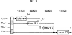
同一異物に対し複数回の照明を行い、該検出された複数の検出信号を加算する方式にフォトダイオード72を使用した場合には、ウエハが一回転する毎に、欠陥散乱光とラフネス散乱光が交互に検出されることになる。つまり一周分の検出信号を蓄積するメモリの切り替え方法も変更する必要がある。
When the
信号処理部151における加算処理方法を図17で説明する。信号処理部151には、欠陥信号蓄積メモリ76とHaze信号蓄積メモリ77がある。
一回転目に欠陥検出画素70aで検出された信号は欠陥信号蓄積メモリ76に蓄積される。二回転目にHaze検出画素71aで検出された信号はHaze信号蓄積メモリ77に蓄積される。三回転目に欠陥検出画素70bで検出された信号は欠陥信号蓄積メモリ76に蓄積される。四回転目にHaze検出画素71bで検出された信号はHaze信号蓄積メモリ77に蓄積される。
以上、欠陥検出画素70a・70bとHaze検出画素71a・71bの二つを有するフォトダイオードアレイ72と、欠陥信号蓄積メモリ76とHaze信号蓄積メモリ77を有し、検出信号を前記二つのメモリに蓄積することにより、偏光検出による欠陥検出感度向上とHaze計測の両立が可能となる。
The addition processing method in the
The signal detected by the
As described above, the
本実施例では4つの画素を有するセンサに関して、欠陥検出画素とHaze検出画素が交互に2個ずつ配置されている例を示しているが、フォトダイオードの画素数、欠陥検出画素とHaze検出画素の比率、配置の順番に制約はない。
例えば、欠陥検出画素が3つで、Haze検出画素が1つとした場合には、欠陥信号の検出回数を3回に増加させることができ、欠陥検出感度向上に効果がある。
フィルタ74a・74bは欠陥散乱光を通過させやすい偏光軸に設定されている例で説明を行ったが、一方の偏光軸を欠陥散乱光が概略最も通過しやすい偏光軸に設定しなくても構わない。センサのダイナミックレンジには限界があるため、微小欠陥を検出するために感度を高めている状態において、大異物から大きな散乱光が発生すると、センサ出力は飽和する場合がある。検出光量に基づき、欠陥寸法を算出するため、センサ出力が飽和すると、欠陥の寸法の算出精度が低下する。欠陥検出画素に装着されているフィルタの偏光軸を、欠陥散乱光が概略最も通過しやすい偏光軸よりずらして設定することにより、大異物から大きな散乱光が発生しても、センサ出力を飽和させずに検出することが可能になり、ダイナミックレンジの拡大に効果がある。
In this embodiment, an example in which two defect detection pixels and two Haze detection pixels are alternately arranged with respect to a sensor having four pixels is shown. However, the number of photodiode pixels, defect detection pixels, and Haze detection pixels There is no restriction on the order of ratio and arrangement.
For example, when there are three defect detection pixels and one Haze detection pixel, the number of detections of the defect signal can be increased to three, which is effective in improving the defect detection sensitivity.
The
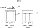
図18は入力部154におけるユーザインターフェースの一例である。検査するウエハの種類を指定するサブウィンドウ180と、各検出器における欠陥信号とHaze信号の抽出・分離率を表示するサブウィンドウ181・182を構成要件とする。
本発明では、検出光学系の配置されている仰角方向と方位角方向は複数あることを特徴としている。一方、欠陥からの散乱光の偏光状態と表面ラフネスからの散乱光の偏光状態は、検出する仰角や方位角に依存して変化する。前記二つの散乱光の有する偏光状態の振動方向が直行する検出条件もあり、また、前記二つの散乱光の有する偏光状態の振動方向が概略同一の方向に偏光している条件も存在する。
FIG. 18 shows an example of a user interface in the
The present invention is characterized in that there are a plurality of elevation angle directions and azimuth angle directions in which the detection optical system is arranged. On the other hand, the polarization state of the scattered light from the defect and the polarization state of the scattered light from the surface roughness change depending on the detected elevation angle and azimuth angle. There are also detection conditions in which the vibration directions of the polarization states of the two scattered lights are orthogonal, and there are also conditions in which the vibration directions of the polarization states of the two scattered lights are polarized in approximately the same direction.
欠陥散乱光と表面ラフネス散乱光の偏光軸が互いに概略直行関係にある検出条件にある検出系であれば、該検出散乱光の中より、欠陥散乱光と表面ラフネス散乱光を減衰させることなく、それぞれ概略100%に近い純度で抽出可能となる。しかし、欠陥散乱光と表面ラフネス散乱光の偏光軸が概略同じである検出条件にある検出系では、原理的に欠陥散乱光と表面ラフネス散乱光の分離検出は困難となる。 If the detection system is in a detection condition in which the polarization axes of the defect scattered light and the surface roughness scattered light are substantially orthogonal to each other, the defect scattered light and the surface roughness scattered light are not attenuated from the detected scattered light, Each can be extracted with a purity of approximately 100%. However, in the detection system under the detection condition in which the polarization axes of the defect scattered light and the surface roughness scattered light are substantially the same, it becomes difficult in principle to separate and detect the defect scattered light and the surface roughness scattered light.
以上のことより、検出方位角・仰角に依存して、欠陥散乱光とラフネス散乱光の分離可能な割合は概略一意に決定され、またその時の偏光検出条件も概略一意に決定することができる。検出方位角・仰角毎の欠陥散乱光とラフネス散乱光の偏光状態をシミュレーションにより事前に計算しておき、欠陥散乱光・ラフネス散乱光の分離率を最大化する検出条件をデータベースとして保存しておくことで、レシピ作成の容易化や作成にかかる時間の短縮が可能になる。 From the above, depending on the detected azimuth angle and elevation angle, the separable ratio of defect scattered light and roughness scattered light is determined approximately uniquely, and the polarization detection conditions at that time can also be determined approximately uniquely. Preliminarily calculate the polarization state of defect scattered light and roughness scattered light for each detected azimuth and elevation angle by simulation, and store the detection conditions that maximize the separation rate of defect scattered light and roughness scattered light as a database This makes it easy to create recipes and shorten the time required for creation.
検査するウエハの材質や表面粗さに応じて、表面ラフネスからの散乱光の偏光状態は変化するため、膜種や表面粗さ毎に欠陥散乱光・ラフネス散乱光の分離率を最大化する検出条件をデータベースとして保存しておくことで、レシピ作成の容易化や作成にかかる時間の短縮が可能になる。 Depending on the material and surface roughness of the wafer to be inspected, the polarization state of the scattered light from the surface roughness changes, so detection that maximizes the separation rate of defect scattered light and roughness scattered light for each film type and surface roughness By storing the conditions as a database, recipe creation can be facilitated and the time required for creation can be shortened.
偏光分離が困難な検出条件でも、信号処理部において周波数帯域別フィルタリングを行うことで、高周波成分を欠陥検出信号、低周波成分をHaze検出信号として分離検出することは可能である。
サブウィンドウ180では、検査する膜種を入力することが可能であり、例えば、Si・Poly-Si・Cu・Al・W・SiO2などがあり、プルダウンで選択可能である。これにより、各検出器での偏光検出条件の初期値が設定され、サブウィンドウ181・182の表示に反映される。
Even under detection conditions where polarization separation is difficult, it is possible to separate and detect a high frequency component as a defect detection signal and a low frequency component as a Haze detection signal by performing frequency band filtering in the signal processing unit.
In the
図18におけるサブウィンドウ181・182では、検出器Aでは欠陥散乱光とラフネス散乱光は偏光検出により減衰することなく分離することができ、概略100%の割合で分離できており、検出器Bでは欠陥散乱光とラフネス散乱光とも偏光検出により20%程度減衰しており、それぞれ概略80%の割合で分離している。
サブウィンドウ181・182の分離率はサブウィンドウ180の選択に応じて、初期値は設定されるが、ユーザが指定することも可能である。例えば、サブウィンドウ181における欠陥散乱光の分離率を80%と設定しても構わないし、サブウィンドウ182の欠陥散乱光分離率を50%にしても構わない。ただし、原理上分離可能な最大の割合は検出条件毎に決まっており、サブウィンドウ内に点線で表示される。分離率をそれ以上に設定することはできない。
入力方法は直接入力でもプルダウン方式でも構わない。
In the sub-windows 181 and 182 in FIG. 18, the detector A can separate the defect scattered light and the roughness scattered light without being attenuated by the polarization detection, and can be separated at a rate of approximately 100%. Both scattered light and roughness scattered light are attenuated by about 20% by polarization detection, and are separated at a rate of approximately 80%.
The initial values of the separation rates of the
The input method may be direct input or pull-down method.
以上のとおり、本発明の実施の形態によれば、偏光検出により欠陥検出感度を向上させ、かつ表面ラフネスからの散乱光を減衰させることなく検出可能となり、欠陥検査とHaze計測とを両立させることが可能となる。
浸透深度の大きい波長帯域のレーザビームを用いることで、ウエハにダメージを与えることなく、照射エネルギの増大が可能となり、検出感度を向上させることが可能となる。
また本発明の実施例によれば、複数画素を有するフォトダイオードアレイを用いた場合、各画素を欠陥検出画素とHaze検出画素に振り分けることで、偏光による検出感度向上とHaze計測を両立可能となる。
As described above, according to the embodiment of the present invention, it is possible to improve the defect detection sensitivity by polarization detection and to detect the scattered light from the surface roughness without attenuating, and to make both defect inspection and Haze measurement compatible. Is possible.
By using a laser beam in a wavelength band with a large penetration depth, irradiation energy can be increased without damaging the wafer, and detection sensitivity can be improved.
According to the embodiment of the present invention, when a photodiode array having a plurality of pixels is used, each pixel is assigned to a defect detection pixel and a Haze detection pixel, thereby making it possible to achieve both improvement in detection sensitivity by polarization and Haze measurement. .
1…ウエハ、2,2a,2b…レーザ光源、3,3a,3b…ビームエキスパンダ、
4,4a,4b…偏光素子、m…ミラー、
6,6a,6b,10a,10b…集光レンズ、8…検出レンズ、9…ビームスプリッタ、
11a,11b,74a,74b,75a,75b…フィルタ、12a,12b…光電子増倍管、
20,21…偏光フィルタ、25…照明スポット、31…浸透深度、
32…浸透深度が小さい物質の特性、33…浸透深度が大きい物質の特性、
34…信号分離機、35…照明スポットの回転方向への長さ、
36…欠陥信号検出器のゲート回路の切り替えタイミング、
37…Haze信号検出器のゲート回路の切り替えタイミング、
40…結像系光学系、41,72…フォトダイオードアレイ、42…集光レンズ、
43…イメージインテンシファイア、44…結像レンズ、50…送りピッチ、60…欠陥、
61a〜61d…フォトダイオードアレイの画素、65…メモリ、
70a,70b…欠陥検出画素、71a,71b…Haze検出画素、
76…欠陥検出信号蓄積メモリ、77…Haze検出信号蓄積メモリ、
101,101a,101b…照明光学系、 102,104a〜104f,105…検出光学系、
102a…欠陥検出光学系、
102b…Haze検出光学系、103…ウエハステージ、
150…アナログ回路、151…信号処理部、152…CPU、153…マップ出力部、
154…入力部、155…ステージ制御部、 160…欠陥マップ、161…Hazeマップ、
170〜174…検査フロー、180〜182…サブウィンドウ、
200,200a,200b…レーザビーム、201…正反射光、202…透過光。
1 ... wafer, 2,2a, 2b ... laser light source, 3,3a, 3b ... beam expander,
4, 4a, 4b ... Polarizing element, m ... Mirror,
6, 6a, 6b, 10a, 10b ... Condensing lens, 8 ... Detection lens, 9 ... Beam splitter,
11a, 11b, 74a, 74b, 75a, 75b ... filter, 12a, 12b ... photomultiplier tube,
20, 21 ... Polarizing filter, 25 ... Lighting spot, 31 ... Penetration depth,
32… Characteristics of substances with
34 ... Signal separator, 35 ... Length in rotation direction of illumination spot,
36 ... Timing of switching the gate circuit of the defect signal detector,
37… Haze signal detector gate circuit switching timing,
40 ... imaging system optical system, 41,72 ... photodiode array, 42 ... condensing lens,
43 ... Image intensifier, 44 ... Imaging lens, 50 ... Feed pitch, 60 ... Defect,
61a to 61d ... photodiode array pixels, 65 ... memory,
70a, 70b ... defect detection pixels, 71a, 71b ... Haze detection pixels,
76 ... Defect detection signal storage memory, 77 ... Haze detection signal storage memory,
101,101a, 101b ... illumination optical system, 102,104a-104f, 105 ... detection optical system,
102a: Defect detection optical system,
102b ... Haze detection optical system, 103 ... wafer stage,
150 ... analog circuit, 151 ... signal processing unit, 152 ... CPU, 153 ... map output unit,
154 ... Input unit, 155 ... Stage control unit, 160 ... Defect map, 161 ... Haze map,
170-174 ... Inspection flow, 180-182 ... Sub-window,
200, 200a, 200b ... laser beam, 201 ... specular reflection light, 202 ... transmitted light.
Claims (20)
前記ウエハ表面に照射するレーザビームを所望の偏光状態に変換する工程と、
変換された前記レーザビームを前記ウエハ表面に照射する工程と、
該レーザビームが照射された前記ウエハ上の被照射領域内から発生する散乱光を、前記ウエハ上の欠陥から発生する第1の散乱光と前記ウエハの表面荒れから発生する第2の散乱光とに分離する工程とを有し、
前記散乱光の分離は、光路分割光学素子を用いて前記第1および第2の散乱光を概略同時のタイミングで行い、各散乱光の検出が前記第1および第2の散乱光の光学属性に基づいて行われることを特徴とする欠陥検査方法。 A defect inspection method for inspecting a surface state including defects on a wafer surface,
Converting a laser beam applied to the wafer surface into a desired polarization state;
Irradiating the wafer surface with the converted laser beam;
Scattered light generated from the irradiated area on the wafer irradiated with the laser beam is converted into first scattered light generated from defects on the wafer and second scattered light generated from surface roughness of the wafer. And a step of separating
The scattered light is separated by using the optical path dividing optical element to perform the first and second scattered lights at substantially the same timing, and the detection of each scattered light is made into the optical attributes of the first and second scattered lights. A defect inspection method which is performed based on the above.
前記レーザビームは、前記ウエハの材質に対する浸透深度が100nm以上となる波長を有することを特徴とする欠陥検査方法。 The defect inspection method according to claim 1,
The defect inspection method according to claim 1, wherein the laser beam has a wavelength at which a penetration depth with respect to the material of the wafer is 100 nm or more.
前記散乱光の分離は、振幅分割、あるいは波長分割、あるいは偏光分割のいずれかの分割手段を用いて行われることを特徴とする欠陥検査方法。 The defect inspection method according to claim 1,
2. The defect inspection method according to claim 1, wherein the scattered light is separated using any one of amplitude division, wavelength division, and polarization division.
前記レーザビームは、波長の異なる複数の光源より放射されることを特徴とする欠陥検査方法。 The defect inspection method according to claim 1,
The defect inspection method, wherein the laser beam is emitted from a plurality of light sources having different wavelengths.
前記分割手段を用いて分離されたそれぞれの散乱光の検出散乱光量は、前記分割手段における分離率を変化させることにより、調整可能であることを特徴とする欠陥検査方法。 The defect inspection method according to claim 3,
A defect inspection method, wherein the detected scattered light amount of each scattered light separated by using the dividing unit can be adjusted by changing a separation rate in the dividing unit.
前記ウエハ表面に対して概略垂直方向からレーザビームを照射することを特徴とする欠陥検査方法。 A defect inspection method according to any one of claims 1 to 5,
A defect inspection method comprising irradiating a laser beam from a direction substantially perpendicular to the wafer surface.
前記ウエハ表面に対して斜方からレーザビームを照射することを特徴とする欠陥検査方法。 A defect inspection method according to any one of claims 1 to 5,
A defect inspection method characterized by irradiating the wafer surface with a laser beam obliquely.
前記ウエハを互いに独立して回転・併進できるステージ上に載置する工程と、
前記ステージの回転・併進を繰り返しながら、レーザビームを前記ウエハ表面の所望の範囲内に照射する工程と、
前記レーザビームが照射された前記ウエハの被照射領域内から発生する散乱光を用いて前記ウエハ上の欠陥判定と、前記ウエハの表面の粗さ状態を判定する表面荒れ判定をする工程とを有し、
前記レーザビームの前記ウエハ上に照明されたビームスポット形状は、前記ステージの回転方向に対する第1のビーム径が、前記ステージの併進方向に対する第2のビーム径より短くなるように設定されていることを特徴とする欠陥検査方法。 A defect inspection method for inspecting a surface state including defects on a wafer surface,
Placing the wafer on a stage that can rotate and translate independently of each other;
Irradiating a laser beam within a desired range of the wafer surface while repeating rotation and translation of the stage; and
A step of determining a defect on the wafer by using scattered light generated from an irradiated area of the wafer irradiated with the laser beam and a surface roughness determination for determining a roughness state of the surface of the wafer. And
The shape of the beam spot of the laser beam illuminated on the wafer is set such that the first beam diameter with respect to the rotation direction of the stage is shorter than the second beam diameter with respect to the translation direction of the stage. Defect inspection method characterized by
信号分離手段と、前記信号分離手段と同期して前記散乱光の透過を制御するフィルタとを備え、
前記第1のビーム径に相当する距離を前記ビームスポットが移動する時間内に、前記欠陥判定を取得する欠陥信号と前記表面荒れ判定を取得するHaze信号とを交互に切り替えて、前記フィルタを通過する前記ウエハ上の被照射領域内から発生した散乱光を、前記ウエハ上の欠陥から発生する第1の散乱光と前記ウエハの表面荒れから発生する第2の散乱光とに分離することを特徴とする欠陥検査方法。 The defect inspection method according to claim 8,
Signal separation means, and a filter that controls transmission of the scattered light in synchronization with the signal separation means,
The defect signal for acquiring the defect determination and the Haze signal for acquiring the surface roughness determination are alternately switched and passed through the filter within the time that the beam spot moves a distance corresponding to the first beam diameter. The scattered light generated from the irradiated area on the wafer is separated into first scattered light generated from defects on the wafer and second scattered light generated from surface roughness of the wafer. Defect inspection method.
前記第2のビームの径が、前記ステージの回転・併進を繰り返しながら前記ウエハ表面の同一領域にレーザビームが複数回照射されるように設定されていることを特徴とする欠陥検査方法。 The defect inspection method according to claim 9,
The defect inspection method, wherein the diameter of the second beam is set so that the same region of the wafer surface is irradiated with the laser beam a plurality of times while repeating the rotation and translation of the stage.
前記同一領域内に存在する欠陥から発生する散乱光をそれぞれの回において検出する第1の検出工程と、
前記同一領域内の表面荒れから発生する散乱光をそれぞれの回において検出する第2の検出工程と、
前記第1の検出工程において検出された複数の信号を加算又は平均化する第1の算出工程と、
前記第2の検出工程において検出された複数の信号を加算又は平均化する第2の算出工程と、
前記第1の算出工程の結果に基づき欠陥判定を行う欠陥判定処理工程と、
前記第2の算出工程の結果に基づき試料表面の粗さ状態を判定する表面荒れ判定工程と、を有し、
前記第1の検出工程と前記第2の検出工程が概略同一のタイミングで行われることを特徴とする欠陥検査方法。 The defect inspection method according to claim 10,
A first detection step of detecting scattered light generated from defects existing in the same region at each time;
A second detection step of detecting scattered light generated from surface roughness in the same region at each time;
A first calculation step of adding or averaging a plurality of signals detected in the first detection step;
A second calculation step of adding or averaging a plurality of signals detected in the second detection step;
A defect determination processing step of performing defect determination based on the result of the first calculation step;
A surface roughness determination step of determining a roughness state of the sample surface based on the result of the second calculation step,
The defect inspection method, wherein the first detection step and the second detection step are performed at substantially the same timing.
前記ウエハ表面に照射するレーザビームを所望の偏光状態に変換する手段と、
変換された前記レーザビームを前記ウエハ表面に照射する光学系と、
該レーザビームが照射された前記ウエハ上の被照射領域内から発生する散乱光を、前記ウエハ上の欠陥から発生する第1の散乱光と前記ウエハの表面荒れから発生する第2の散乱光とに分離する手段と、を有し、
前記散乱光の分離は、光路分割光学素子を用いて前記第1の散乱と前記第2の散乱光を概略同一のタイミングで行い、各散乱光の検出が前記第1および第2の散乱光のそれぞれの光学属性に基づいて行われることを特徴とする欠陥検査装置。 A defect inspection apparatus for inspecting a surface state including defects on a wafer surface,
Means for converting a laser beam applied to the wafer surface into a desired polarization state;
An optical system for irradiating the wafer surface with the converted laser beam;
Scattered light generated from the irradiated area on the wafer irradiated with the laser beam is converted into first scattered light generated from defects on the wafer and second scattered light generated from surface roughness of the wafer. And means for separating
The scattered light is separated by using the optical path dividing optical element to perform the first scattered light and the second scattered light at substantially the same timing, and each scattered light is detected by the first and second scattered lights. A defect inspection apparatus, which is performed based on each optical attribute.
前記第1の散乱光を検出する第1の検出光学系と、
前記第2の散乱光を検出する第2の検出光学系と、
前記第1の検出光学系で検出された前記第1の散乱光を信号に変換し、該信号に基づき欠陥判定を行う第1の信号処理部と、
前記第2の検出光学系で検出された前記第2の散乱光を信号に変換し、該信号に基づきウエハ表面の粗さ状態を解析する第2の信号処理部とを有することを特徴とする欠陥検査装置。 The defect inspection apparatus according to claim 12,
A first detection optical system for detecting the first scattered light;
A second detection optical system for detecting the second scattered light;
A first signal processing unit that converts the first scattered light detected by the first detection optical system into a signal, and performs defect determination based on the signal;
And a second signal processing unit that converts the second scattered light detected by the second detection optical system into a signal and analyzes the roughness state of the wafer surface based on the signal. Defect inspection equipment.
前記レーザビームは、前記ウエハの材質に対する浸透深度が100nm以上となる波長を有することを特徴とする欠陥検査装置。 The defect inspection apparatus according to claim 12 or 13,
The defect inspection apparatus according to claim 1, wherein the laser beam has a wavelength at which a penetration depth with respect to a material of the wafer is 100 nm or more.
前記ウエハを保持し、回転機構および併進移動機構のそれぞれによりウエハを回転・併進移動させるステージと、
前記ウエハ表面での照明領域がウエハ上において長手方向に延在しその長手方向に直交する方向に所定の幅を有する概略線状となるようにレーザビームを照射する照明光学系と、
前記照明によりウエハ被照射領域内から発生する散乱光を検出する検出光学系と、を有し、
前記回転機構によりステージが360度回転する期間に前記併進移動機構によりステージが移動する距離が、前記ウエハ表面の概略線状照明領域の長手方向の長さの半分よりも短い距離であることを特徴とする欠陥検査装置。 The defect inspection apparatus according to claim 12,
A stage for holding the wafer and rotating / translating the wafer by each of a rotation mechanism and a translation mechanism;
An illumination optical system for irradiating a laser beam so that an illumination area on the wafer surface extends in a longitudinal direction on the wafer and has a substantially linear shape in a direction perpendicular to the longitudinal direction;
A detection optical system that detects scattered light generated from within the wafer irradiation area by the illumination, and
The distance by which the stage is moved by the translation mechanism during a period in which the stage is rotated 360 degrees by the rotation mechanism is shorter than half the length of the substantially linear illumination region on the wafer surface in the longitudinal direction. Defect inspection equipment.
前記検出光学系は、偏光検出フィルタを有し、
前記偏光検出フィルタは、光軸を中心に回転することにより検出する偏光軸を調節可能であることを特徴とする欠陥検査装置。 The defect inspection apparatus according to any one of claims 13 to 15,
The detection optical system has a polarization detection filter,
The defect inspection apparatus, wherein the polarization detection filter is capable of adjusting a polarization axis to be detected by rotating about an optical axis.
前記第1および第2の検出光学系を一組とする複数組の検出光学系を有することを特徴とする欠陥検査装置。 The defect inspection apparatus according to claim 13 or 15,
A defect inspection apparatus comprising a plurality of detection optical systems each including the first and second detection optical systems.
前記複数組の検出光学系は、前記ウエハに対して互いに異なる仰角を有することを特徴とする欠陥検査装置。 The defect inspection apparatus according to claim 17,
The defect inspection apparatus, wherein the plurality of sets of detection optical systems have mutually different elevation angles with respect to the wafer.
前記複数組の検出光学系は、前記ウエハに対して互いに異なる方位角を有することを特徴とする欠陥検査装置。 The defect inspection apparatus according to claim 17,
The defect inspection apparatus, wherein the plurality of sets of detection optical systems have different azimuth angles with respect to the wafer.
前記第1および前記第2の散乱光をそれぞれ検出する第1および第2の検出光学系と、
ユーザが検査に必要な情報を表示するインターフェースとを有し、
前記インターフェースにおいて、ウエハの種類を選択する第1のサブウィンドウと、
前記ウエハを検査する時の前記第1および第2の検出光学系における検出偏光状態を表示する第2のサブウィンドウとを有することを特徴とする欠陥検査装置。 The defect inspection apparatus according to claim 12,
First and second detection optical systems for detecting the first and second scattered light, respectively;
An interface for displaying information necessary for inspection by the user,
A first sub-window for selecting a wafer type in the interface;
A defect inspection apparatus comprising: a second sub-window for displaying a detected polarization state in the first and second detection optical systems when inspecting the wafer.
Priority Applications (6)
| Application Number | Priority Date | Filing Date | Title |
|---|---|---|---|
| JP2009045857A JP2010197352A (en) | 2009-02-27 | 2009-02-27 | Defect inspection method and defect inspecting apparatus |
| PCT/JP2009/006887 WO2010097878A1 (en) | 2009-02-27 | 2009-12-15 | Defect inspecting method and defect inspecting apparatus |
| US13/146,428 US8638429B2 (en) | 2009-02-27 | 2009-12-15 | Defect inspecting method and defect inspecting apparatus |
| US14/154,612 US9228960B2 (en) | 2009-02-27 | 2014-01-14 | Defect inspecting method and defect inspecting apparatus |
| US14/986,824 US9841384B2 (en) | 2009-02-27 | 2016-01-04 | Defect inspecting method and defect inspecting apparatus |
| US15/806,937 US10254235B2 (en) | 2009-02-27 | 2017-11-08 | Defect inspecting method and defect inspecting apparatus |
Applications Claiming Priority (1)
| Application Number | Priority Date | Filing Date | Title |
|---|---|---|---|
| JP2009045857A JP2010197352A (en) | 2009-02-27 | 2009-02-27 | Defect inspection method and defect inspecting apparatus |
Publications (1)
| Publication Number | Publication Date |
|---|---|
| JP2010197352A true JP2010197352A (en) | 2010-09-09 |
Family
ID=42665104
Family Applications (1)
| Application Number | Title | Priority Date | Filing Date |
|---|---|---|---|
| JP2009045857A Pending JP2010197352A (en) | 2009-02-27 | 2009-02-27 | Defect inspection method and defect inspecting apparatus |
Country Status (3)
| Country | Link |
|---|---|
| US (4) | US8638429B2 (en) |
| JP (1) | JP2010197352A (en) |
| WO (1) | WO2010097878A1 (en) |
Cited By (6)
| Publication number | Priority date | Publication date | Assignee | Title |
|---|---|---|---|---|
| WO2012090392A1 (en) * | 2010-12-27 | 2012-07-05 | 株式会社 日立ハイテクノロジーズ | Measuring device |
| WO2012090367A1 (en) * | 2010-12-27 | 2012-07-05 | 株式会社日立ハイテクノロジーズ | Defect inspection method and defect inspection device |
| WO2012082501A3 (en) * | 2010-12-16 | 2012-08-16 | Kla-Tencor Corporation | Wafer inspection |
| JP2015038423A (en) * | 2011-08-02 | 2015-02-26 | レーザーテック株式会社 | Device and method for pattern inspection, and method for fabricating pattern substrate |
| JP2016014661A (en) * | 2014-06-19 | 2016-01-28 | ザ・ボーイング・カンパニーTheBoeing Company | System and method for detecting pin holes in fiberglass and composite parts |
| US9279774B2 (en) | 2011-07-12 | 2016-03-08 | Kla-Tencor Corp. | Wafer inspection |
Families Citing this family (16)
| Publication number | Priority date | Publication date | Assignee | Title |
|---|---|---|---|---|
| US7710557B2 (en) * | 2007-04-25 | 2010-05-04 | Hitachi High-Technologies Corporation | Surface defect inspection method and apparatus |
| JP2010197352A (en) * | 2009-02-27 | 2010-09-09 | Hitachi High-Technologies Corp | Defect inspection method and defect inspecting apparatus |
| JP2013178231A (en) * | 2012-02-01 | 2013-09-09 | Canon Inc | Inspection device, inspection method, lithography device and imprinting device |
| JP2013160629A (en) * | 2012-02-06 | 2013-08-19 | Hitachi High-Technologies Corp | Defect inspection method, defect inspection apparatus, program, and output unit |
| JP5773939B2 (en) * | 2012-04-27 | 2015-09-02 | 株式会社日立ハイテクノロジーズ | Defect inspection apparatus and defect inspection method |
| JP5946751B2 (en) * | 2012-11-08 | 2016-07-06 | 株式会社日立ハイテクノロジーズ | Defect detection method and apparatus, and defect observation method and apparatus |
| CN105900418B (en) * | 2013-02-18 | 2018-01-12 | 卡帝瓦公司 | The system, apparatus and method of the quality evaluation of OLED stack film |
| CN103604814A (en) * | 2013-10-23 | 2014-02-26 | 上海华力微电子有限公司 | Detection method for chip defect |
| US11300773B2 (en) | 2014-09-29 | 2022-04-12 | Agilent Technologies, Inc. | Mid-infrared scanning system |
| US9546905B1 (en) * | 2015-04-10 | 2017-01-17 | Agilent Technologies, Inc. | Mid-infrared scanning system that differentiates between specular and diffuse scattering |
| US9804098B2 (en) * | 2015-10-20 | 2017-10-31 | Taiwan Semiconductor Manufacturing Co., Ltd. | Defect recognition system and defect recognition method |
| FR3045156B1 (en) * | 2015-12-11 | 2017-12-22 | Soitec Silicon On Insulator | FAULT DETECTION METHOD AND DEVICE THEREFOR |
| TW201918700A (en) | 2017-05-05 | 2019-05-16 | 美商3M新設資產公司 | Scatterometry system and method of using the same |
| WO2019159334A1 (en) * | 2018-02-16 | 2019-08-22 | 株式会社日立ハイテクノロジーズ | Defect inspection device |
| CN115165758A (en) | 2018-07-06 | 2022-10-11 | 深圳中科飞测科技股份有限公司 | Detection equipment and method |
| US11138722B2 (en) * | 2018-12-21 | 2021-10-05 | Kla-Tencor Corporation | Differential imaging for single-path optical wafer inspection |
Citations (6)
| Publication number | Priority date | Publication date | Assignee | Title |
|---|---|---|---|---|
| JPH07294422A (en) * | 1994-04-27 | 1995-11-10 | Mitsubishi Materials Corp | Detecting method for surface vicinity crystal defect and device therefor |
| JPH10293102A (en) * | 1998-05-11 | 1998-11-04 | Mitsui Mining & Smelting Co Ltd | Detecting method of defect in semiconductor or the like |
| JPH11258175A (en) * | 1998-03-13 | 1999-09-24 | Shin Etsu Handotai Co Ltd | Foreign matter inspection method |
| JP2001083080A (en) * | 1999-09-13 | 2001-03-30 | Hitachi Ltd | Crystal defect measuring device |
| JP2008268140A (en) * | 2007-04-25 | 2008-11-06 | Hitachi High-Technologies Corp | Defect inspection method and device |
| JP2009511878A (en) * | 2005-10-06 | 2009-03-19 | ケーエルエー−テンカー テクノロジィース コーポレイション | Method and system for inspecting wafers |
Family Cites Families (24)
| Publication number | Priority date | Publication date | Assignee | Title |
|---|---|---|---|---|
| US4286843A (en) * | 1979-05-14 | 1981-09-01 | Reytblatt Zinovy V | Polariscope and filter therefor |
| US5486919A (en) * | 1992-04-27 | 1996-01-23 | Canon Kabushiki Kaisha | Inspection method and apparatus for inspecting a particle, if any, on a substrate having a pattern |
| JP3686160B2 (en) | 1995-04-10 | 2005-08-24 | 株式会社日立ハイテクノロジーズ | Wafer surface inspection method and inspection apparatus |
| US5903342A (en) * | 1995-04-10 | 1999-05-11 | Hitachi Electronics Engineering, Co., Ltd. | Inspection method and device of wafer surface |
| DE19535392A1 (en) * | 1995-09-23 | 1997-03-27 | Zeiss Carl Fa | Radial polarization-rotating optical arrangement and microlithography projection exposure system with it |
| US6034776A (en) | 1997-04-16 | 2000-03-07 | The United States Of America As Represented By The Secretary Of Commerce | Microroughness-blind optical scattering instrument |
| US6757056B1 (en) * | 2001-03-26 | 2004-06-29 | Candela Instruments | Combined high speed optical profilometer and ellipsometer |
| JP2000162141A (en) | 1998-11-27 | 2000-06-16 | Hitachi Ltd | Defect inspecting device and method |
| US7061601B2 (en) * | 1999-07-02 | 2006-06-13 | Kla-Tencor Technologies Corporation | System and method for double sided optical inspection of thin film disks or wafers |
| JP2003130808A (en) * | 2001-10-29 | 2003-05-08 | Hitachi Ltd | Method and device for defect inspection |
| US7433031B2 (en) * | 2003-10-29 | 2008-10-07 | Core Tech Optical, Inc. | Defect review system with 2D scanning and a ring detector |
| US7110106B2 (en) * | 2003-10-29 | 2006-09-19 | Coretech Optical, Inc. | Surface inspection system |
| TWI366219B (en) * | 2004-02-06 | 2012-06-11 | Nikon Corp | Polarization changing device, optical illumination apparatus, light-exposure apparatus and light-exposure method |
| US7304719B2 (en) * | 2004-03-31 | 2007-12-04 | Asml Holding N.V. | Patterned grid element polarizer |
| US7324280B2 (en) * | 2004-05-25 | 2008-01-29 | Asml Holding N.V. | Apparatus for providing a pattern of polarization |
| US20060192949A1 (en) * | 2004-12-19 | 2006-08-31 | Bills Richard E | System and method for inspecting a workpiece surface by analyzing scattered light in a back quartersphere region above the workpiece |
| US20070058151A1 (en) * | 2005-09-13 | 2007-03-15 | Asml Netherlands B.V. | Optical element for use in lithography apparatus and method of conditioning radiation beam |
| EP1932061A1 (en) * | 2005-10-04 | 2008-06-18 | Carl Zeiss SMT AG | Device and method for influencing polarisation distribution in an optical system, in particular in a microlithography exposure system |
| US7714997B2 (en) * | 2006-11-07 | 2010-05-11 | Hitachi High-Technologies Corporation | Apparatus for inspecting defects |
| JP4638864B2 (en) * | 2006-12-20 | 2011-02-23 | 株式会社日立ハイテクノロジーズ | Sample surface defect inspection system |
| US7710557B2 (en) | 2007-04-25 | 2010-05-04 | Hitachi High-Technologies Corporation | Surface defect inspection method and apparatus |
| JP5466377B2 (en) * | 2008-05-16 | 2014-04-09 | 株式会社日立ハイテクノロジーズ | Defect inspection equipment |
| JP5624714B2 (en) * | 2008-05-23 | 2014-11-12 | 株式会社日立ハイテクノロジーズ | Inspection method and inspection apparatus for substrate surface |
| JP2010197352A (en) * | 2009-02-27 | 2010-09-09 | Hitachi High-Technologies Corp | Defect inspection method and defect inspecting apparatus |
-
2009
- 2009-02-27 JP JP2009045857A patent/JP2010197352A/en active Pending
- 2009-12-15 US US13/146,428 patent/US8638429B2/en not_active Expired - Fee Related
- 2009-12-15 WO PCT/JP2009/006887 patent/WO2010097878A1/en active Application Filing
-
2014
- 2014-01-14 US US14/154,612 patent/US9228960B2/en active Active
-
2016
- 2016-01-04 US US14/986,824 patent/US9841384B2/en active Active
-
2017
- 2017-11-08 US US15/806,937 patent/US10254235B2/en active Active
Patent Citations (6)
| Publication number | Priority date | Publication date | Assignee | Title |
|---|---|---|---|---|
| JPH07294422A (en) * | 1994-04-27 | 1995-11-10 | Mitsubishi Materials Corp | Detecting method for surface vicinity crystal defect and device therefor |
| JPH11258175A (en) * | 1998-03-13 | 1999-09-24 | Shin Etsu Handotai Co Ltd | Foreign matter inspection method |
| JPH10293102A (en) * | 1998-05-11 | 1998-11-04 | Mitsui Mining & Smelting Co Ltd | Detecting method of defect in semiconductor or the like |
| JP2001083080A (en) * | 1999-09-13 | 2001-03-30 | Hitachi Ltd | Crystal defect measuring device |
| JP2009511878A (en) * | 2005-10-06 | 2009-03-19 | ケーエルエー−テンカー テクノロジィース コーポレイション | Method and system for inspecting wafers |
| JP2008268140A (en) * | 2007-04-25 | 2008-11-06 | Hitachi High-Technologies Corp | Defect inspection method and device |
Cited By (11)
| Publication number | Priority date | Publication date | Assignee | Title |
|---|---|---|---|---|
| WO2012082501A3 (en) * | 2010-12-16 | 2012-08-16 | Kla-Tencor Corporation | Wafer inspection |
| JP2014504370A (en) * | 2010-12-16 | 2014-02-20 | ケーエルエー−テンカー コーポレイション | Wafer inspection |
| US8891079B2 (en) | 2010-12-16 | 2014-11-18 | Kla-Tencor Corp. | Wafer inspection |
| WO2012090392A1 (en) * | 2010-12-27 | 2012-07-05 | 株式会社 日立ハイテクノロジーズ | Measuring device |
| WO2012090367A1 (en) * | 2010-12-27 | 2012-07-05 | 株式会社日立ハイテクノロジーズ | Defect inspection method and defect inspection device |
| JP2012137350A (en) * | 2010-12-27 | 2012-07-19 | Hitachi High-Technologies Corp | Defect inspection method and device |
| US8922764B2 (en) | 2010-12-27 | 2014-12-30 | Hitachi High-Technologies Corporation | Defect inspection method and defect inspection apparatus |
| US8958076B2 (en) | 2010-12-27 | 2015-02-17 | Hitachi High-Technologies Corporation | Surface shape measuring apparatus |
| US9279774B2 (en) | 2011-07-12 | 2016-03-08 | Kla-Tencor Corp. | Wafer inspection |
| JP2015038423A (en) * | 2011-08-02 | 2015-02-26 | レーザーテック株式会社 | Device and method for pattern inspection, and method for fabricating pattern substrate |
| JP2016014661A (en) * | 2014-06-19 | 2016-01-28 | ザ・ボーイング・カンパニーTheBoeing Company | System and method for detecting pin holes in fiberglass and composite parts |
Also Published As
| Publication number | Publication date |
|---|---|
| US10254235B2 (en) | 2019-04-09 |
| US20180067060A1 (en) | 2018-03-08 |
| US8638429B2 (en) | 2014-01-28 |
| US20120019835A1 (en) | 2012-01-26 |
| WO2010097878A1 (en) | 2010-09-02 |
| US9228960B2 (en) | 2016-01-05 |
| US9841384B2 (en) | 2017-12-12 |
| US20140125980A1 (en) | 2014-05-08 |
| US20160116421A1 (en) | 2016-04-28 |
Similar Documents
| Publication | Publication Date | Title |
|---|---|---|
| WO2010097878A1 (en) | Defect inspecting method and defect inspecting apparatus | |
| TWI722246B (en) | Defect marking for semiconductor wafer inspection | |
| JP4500641B2 (en) | Defect inspection method and apparatus | |
| TWI656338B (en) | Time delay integral sensor in dark field system | |
| JP5520736B2 (en) | Defect inspection method and defect inspection apparatus | |
| JP5349742B2 (en) | Surface inspection method and surface inspection apparatus | |
| JP5417205B2 (en) | Defect inspection apparatus and defect inspection method | |
| TWI713638B (en) | Method for detecting defects and associated device | |
| US9255891B2 (en) | Inspection beam shaping for improved detection sensitivity | |
| JP6214323B2 (en) | Device for distinguishing between dissimilar and unique surface features | |
| US7773212B1 (en) | Contemporaneous surface and edge inspection | |
| TW201932828A (en) | System for wafer inspection | |
| JP2009244035A (en) | Method and its apparatus for inspecting defects | |
| US11138722B2 (en) | Differential imaging for single-path optical wafer inspection | |
| WO2013025376A1 (en) | Large particle detection for multi-spot surface scanning inspection systems | |
| JP2008096430A (en) | Method and apparatus for detecting defect | |
| US7130036B1 (en) | Methods and systems for inspection of an entire wafer surface using multiple detection channels | |
| US9746430B2 (en) | Optical inspecting apparatus | |
| JP2011069659A (en) | Flaw inspection method and flaw inspection system | |
| JP2002116155A (en) | Apparatus and method for inspecting foreign matter and defect | |
| JP5760066B2 (en) | Defect inspection apparatus and defect inspection method | |
| EP3987567A1 (en) | Combined transmitted and reflected light imaging of internal cracks in semiconductor devices | |
| JP5668113B2 (en) | Defect inspection equipment | |
| JP2014178215A (en) | Inspection equipment |
Legal Events
| Date | Code | Title | Description |
|---|---|---|---|
| A621 | Written request for application examination |
Free format text: JAPANESE INTERMEDIATE CODE: A621 Effective date: 20110919 |
|
| A131 | Notification of reasons for refusal |
Free format text: JAPANESE INTERMEDIATE CODE: A131 Effective date: 20121113 |
|
| A521 | Written amendment |
Free format text: JAPANESE INTERMEDIATE CODE: A523 Effective date: 20130110 |
|
| A02 | Decision of refusal |
Free format text: JAPANESE INTERMEDIATE CODE: A02 Effective date: 20130730 |