JP2010152913A - Organization of blocks within nonvolatile memory unit to effectively decrease sector write operation time - Google Patents
Organization of blocks within nonvolatile memory unit to effectively decrease sector write operation time Download PDFInfo
- Publication number
- JP2010152913A JP2010152913A JP2010031847A JP2010031847A JP2010152913A JP 2010152913 A JP2010152913 A JP 2010152913A JP 2010031847 A JP2010031847 A JP 2010031847A JP 2010031847 A JP2010031847 A JP 2010031847A JP 2010152913 A JP2010152913 A JP 2010152913A
- Authority
- JP
- Japan
- Prior art keywords
- sector
- block
- information
- sector information
- flash device
- Prior art date
- Legal status (The legal status is an assumption and is not a legal conclusion. Google has not performed a legal analysis and makes no representation as to the accuracy of the status listed.)
- Pending
Links
Images


Classifications
-
- G—PHYSICS
- G11—INFORMATION STORAGE
- G11C—STATIC STORES
- G11C8/00—Arrangements for selecting an address in a digital store
- G11C8/12—Group selection circuits, e.g. for memory block selection, chip selection, array selection
-
- G—PHYSICS
- G11—INFORMATION STORAGE
- G11C—STATIC STORES
- G11C16/00—Erasable programmable read-only memories
- G11C16/02—Erasable programmable read-only memories electrically programmable
- G11C16/06—Auxiliary circuits, e.g. for writing into memory
- G11C16/08—Address circuits; Decoders; Word-line control circuits
-
- G—PHYSICS
- G11—INFORMATION STORAGE
- G11C—STATIC STORES
- G11C16/00—Erasable programmable read-only memories
- G11C16/02—Erasable programmable read-only memories electrically programmable
- G11C16/06—Auxiliary circuits, e.g. for writing into memory
- G11C16/10—Programming or data input circuits
- G11C16/102—External programming circuits, e.g. EPROM programmers; In-circuit programming or reprogramming; EPROM emulators
Landscapes
- Engineering & Computer Science (AREA)
- Microelectronics & Electronic Packaging (AREA)
- Techniques For Improving Reliability Of Storages (AREA)
- Read Only Memory (AREA)
- Memory System (AREA)
- Signal Processing For Digital Recording And Reproducing (AREA)
Abstract
Description
(発明の背景)
(関連出願の相互参照)
本出願は、以前に出願された米国特許出願第09/283,728号、および他の以前に出願された米国特許出願第09/264,340号の一部継続出願である。米国特許出願第09/283,728号は、「SPACE MANAGEMENT FOR MANAGING HIGH CAPACITY NONVOLATILE MEMORY」という名称であり、1999年4月1日に出願され、発明者がPetro Estakhri、Berhanu Iman、およびMin Guoである。米国特許出願第09/264,340号は、「MOVING SECTORS WITHIN A BLOCK OF INFORMATION IN A FLASH MEMORY MASS STORAGE ARCHITECTURE」という名称であり、1999年3月8日に出願され、発明者が、Petro Estakhri、Berhanu Iman、およびAli Ganjueiであり、1999年5月25日に発行された米国特許第5,907,856号、および、以前に出願された、米国特許出願第09/030,697号の継続出願である。米国特許第5,907,856号は、「MOVING SECTORS WITHIN A BLOCK OF INFORMATION IN A FLASH MEMORY MASS STORAGE ARCHITECTURE」という名称である。米国特許出願第09/030,697号は、「INCREASING MEMORY PERFORMANCE IN FLASH MEMORY DEVICES BY PERFORMING SIMULTANEOUS WRITE OPERATION TO MULTIPLE DEVICES」という名称であり、1998年2月25日に出願され、発明者が、Petro EstakhriおよびBerhanu Imanである。これらの特許の開示内容の全ては、全文が記載されているかのように、本明細書中で参考として援用される。
(Background of the Invention)
(Cross-reference of related applications)
This application is a continuation-in-part of previously filed US patent application Ser. No. 09 / 283,728 and other previously filed US patent application Ser. No. 09 / 264,340. US patent application Ser. No. 09 / 283,728 is entitled “SPACE MANAGEMENT FOR MANAGING HIGH CAPACITY NONVOLATILE MEMORY” and was filed on April 1, 1999, inventor Petro Estakri, Berhanu Iman, Berhanu Iman, is there. US Patent Application No. 09 / 264,340 is named “MOVING SECTORS WITHIN A BLOCK OF INFORMATION IN A FLASH MEMORY MASS STORE ARCHITECTURE”, filed on March 8, 1999, with the Berhanu Iman and Ali Ganjuei, U.S. Pat. No. 5,907,856 issued on May 25, 1999, and continuation of previously filed U.S. Patent Application No. 09 / 030,697 It is. US Pat. No. 5,907,856 is entitled “MOVING SECTORS WITHIN BLOCK OF INFORMATION IN A FLASH MEMORY MASS STORE ARCHITECTURE”. US patent application No. 09 / 030,697 is “INCREASING MEMORY PERFORMANCE IN FLASH MEMORY DEVICES BY PERFORMING SIMULTANEOUS WRITE OPERATION TO MULTIPLE on May 25”. And Berhanu Iman. The entire disclosures of these patents are hereby incorporated by reference as if set forth in full.
(発明の分野)
本発明は、概して、フラッシュメモリのような不揮発性メモリデバイスを採用するデジタル格納システムの分野、特に、情報を不揮発性メモリデバイスに書き込むことにかかる時間を低減して、システム性能全体を高めることに関する。
(Field of Invention)
The present invention relates generally to the field of digital storage systems that employ non-volatile memory devices such as flash memory, and in particular to reducing overall time taken to write information to non-volatile memory devices and increasing overall system performance. .
(従来技術の説明)
近年、固体メモリは、様々な技術領域、例えば、コンピュータ、デジタルカメラ、モデムなどにおける、大容量記憶装置機器の代わりとしての使用において、人気が高まってきた。例えば、デジタルカメラにおいて、フラッシュメモリのような固体メモリは、従来のフィルムの代わりに用いられている。
(Description of prior art)
In recent years, solid state memory has become increasingly popular for use as an alternative to mass storage devices in various technical areas, such as computers, digital cameras, modems, and the like. For example, in a digital camera, a solid state memory such as a flash memory is used instead of a conventional film.
フラッシュメモリは、概して、半導体デバイス(または、チップ)の形態で提供され、各デバイスは、多数のトランジスタメモリセルで作られ、各セルは、個別にプログラマブルである。このようなメモリセルのプログラミング(もしくは、書き込み)、および消去は、消去−書き込みサイクルが有限の回数に制限され、基本的にデバイスの寿命を定めている。さらに、フラッシュメモリセルの固有の特徴は、プログラムされる前に、消去され、消去が成功したかどうか確認される必要があることである。 Flash memory is generally provided in the form of semiconductor devices (or chips), each device made of a number of transistor memory cells, each cell individually programmable. Such programming (or writing) and erasing of a memory cell basically limits the lifetime of the device by limiting the number of erase-write cycles to a finite number of times. Furthermore, an inherent feature of flash memory cells is that they must be erased and verified for successful erase before being programmed.
従って、フラッシュメモリを用いることによって、一度情報を含んだメモリの領域を、同じ領域を再プログラムするたびに、その前に消去することが必要になる。フラッシュメモリデバイスにおいて、書き込みおよび消去サイクルは、概して、時間がかかるものであり、そのことによって、大容量記憶装置としてフラッシュメモリを利用するシステムの性能が大幅に低下する。 Therefore, by using the flash memory, it is necessary to erase the area of the memory once containing information before reprogramming the same area. In flash memory devices, write and erase cycles are generally time consuming, which significantly reduces the performance of systems that utilize flash memory as a mass storage device.
フラッシュメモリデバイスを採用する適用例、例えば、パーソナルコンピュータおよびデジタルカメラにおいて、ホストは、通常は半導体デバイスの形態のコントローラデバイスを介して、情報を、フラッシュメモリデバイスに書き込んだり、フラッシュメモリデバイスから読み出す。このような情報は、セクタに編成され、各セクタは、ユーザデータ情報およびオーバーヘッド情報(まとめて、セクタ情報と呼ばれる)を含む。セクタのユーザデータ部分は、典型的には、長さが512バイトであるが、他のサイズのセクタも同様に採用され得る。コントローラは、ホストが命令した書き込み動作中に、ホストからセクタ情報を受信すると、所定のセクタ編成に従って、セクタ情報をフラッシュメモリデバイスに書き込む。ホストが複数のセクタにアクセスし得る間、各セクタは、1度に1つずつフラッシュデバイスに書き込まれる。 In applications that employ flash memory devices, such as personal computers and digital cameras, the host writes information to and reads information from the flash memory device, typically via a controller device in the form of a semiconductor device. Such information is organized into sectors, each sector including user data information and overhead information (collectively referred to as sector information). The user data portion of the sector is typically 512 bytes in length, but other size sectors may be employed as well. When the controller receives sector information from the host during a write operation commanded by the host, the controller writes the sector information to the flash memory device according to a predetermined sector organization. While the host can access multiple sectors, each sector is written to the flash device one at a time.
データファイル(データファイルは、商業的ソフトウェア、ユーザプログラム、ワードプロセッサソフトウェア文書、拡張シートファイルなどを含む、任意のコンピュータファイルであり得る)の格納および/または取り出しにおいて、コンピュータ(または、ホスト)システムは、データファイルが大容量記憶装置内で存在するとホストが考えるロケーションを示す、論理ブロックアドレスと呼ばれるものを提供する。ホストが提供するアドレスは、コントローラによって受信されると論理ブロックアドレスフォーマットに変換される、シリンダー、ヘッダおよびセクタ(CHS)の形態であり得る。同じことが、デジタルカメラの適用例にもあてはまる。その後、コントローラは、論理ブロックアドレス(LBA)を、仮想論理ブロックアドレス(VLBA)に変換し、後者を用いて、空間マネージャ参照テーブル(LUT)内の仮想物理的ブロックアドレス(VPBA)を参照する。VPBAを取り出すと、コントローラは、VPBAを用いて、フラッシュメモリ内のデータファイルにアクセスする。データファイルは、不揮発性メモリ内の、所定の数のセクタを有するブロックに格納される。例えば、ブロックは、16個のセクタを含み、各セクタは、512バイトのユーザデータ情報、および様々なバイトの拡張またはオーバーヘッド情報(例えば、フラグ、ECCなど)を含む。VPBAは、不揮発性メモリ内の特定のブロックのロケーションを特定するために、PBAに変換される。 In storing and / or retrieving data files (data files can be any computer file, including commercial software, user programs, word processor software documents, expansion sheet files, etc.), the computer (or host) system can: It provides what is called a logical block address that indicates the location that the host considers that the data file is present in the mass storage device. The address provided by the host may be in the form of a cylinder, header and sector (CHS) that is converted to a logical block address format when received by the controller. The same applies to digital camera applications. Thereafter, the controller converts the logical block address (LBA) into a virtual logical block address (VLBA), and refers to the virtual physical block address (VPBA) in the space manager reference table (LUT) using the latter. When the VPBA is taken out, the controller uses the VPBA to access the data file in the flash memory. The data file is stored in a block having a predetermined number of sectors in the non-volatile memory. For example, a block includes 16 sectors, each sector containing 512 bytes of user data information, and various byte extensions or overhead information (eg, flags, ECC, etc.). The VPBA is converted to PBA to identify the location of a particular block in non-volatile memory.
データファイルが変更されるたびに、最新バージョンのファイルが、新たな物理的ロケーション(または、新たなPBA)によって識別されるフラッシュメモリ内の利用可能な(または、「使用されていない」)ロケーションに格納される。更新されたファイル用に、フラッシュメモリ内の空き(利用可能な)ロケーションの多くを用いると、さらなる情報の格納用に利用可能な「古い」ロケーションを作るために、消去動作が必要となり得る。消去動作に(書き込み動作と同様に)時間がかかるため、次の消去動作の前により多くのロケーションが用いられれれば用いられるほど、消去動作を行う頻度と、フラッシュメモリ内の空きロケーションを探すための時間との間でトレードオフがある。消去動作の回数を低減するか、または、不揮発性メモリ内の情報のブロックのロケーションの特定に関連する検索にかかる時間を低減することによって、システム性能を向上させるための方法を試み、探す努力が絶え間なく行われている。 Each time a data file changes, the latest version of the file is placed in an available (or “unused”) location in flash memory identified by a new physical location (or new PBA). Stored. Using many of the free (available) locations in the flash memory for updated files, an erase operation may be required to create an “old” location that is available for storing additional information. Since the erase operation takes time (similar to the write operation), the more locations are used before the next erase operation, the more often the location is used to find the frequency of the erase operation and the free location in the flash memory. There is a trade-off with time. Efforts to try and find ways to improve system performance by reducing the number of erase operations or by reducing the time taken to search for the location of a block of information in non-volatile memory It is done continuously.
不揮発性メモリまたはフラッシュメモリ内の情報は、コントローラの方向の下に格納され、セクタの形態で行われ、複数のセクタがブロックの境界を定める。ブロックは、16個、32個、または他の個数のセクタを含み得る。ブロックが所定の数のセクタを含むことが決定されると、この決定されたサイズが各ブロックの境界を規定する。従って、不揮発性メモリに格納された情報が、ブロックに編成され、各ブロックは、コントローラによって一意的にアドレス可能である。さらに、各ブロックは複数のセクタからなり、各セクタは、512バイトと、データ以外の情報、例えば、フラグ、アドレスおよびエラー訂正コード(ECCを格納するためのさらなる格納空間とによって規定される。しかし、セクタは、512バイト以外のデータ格納空間を有してもよい。いくつかの従来技術によるシステムにおいて、消去動作中、ブロック全体が消去されるが、他の従来技術によるシステムにおいて、セクタが消去され得る。ブロック内の各セクタは、不揮発性メモリから情報を読み出したり、不揮発性メモリに情報を書き込んだりするために、一意的にアドレス可能である。一意的な値は、起動中に、複発性メモリに関連するアドレスまたはマッピング情報の再構成において用いられる、仮想論理ブロックアドレス(VBLA)として、セクタ情報を含む各ブロック内で維持される。当業者にとって周知であるように、電力が失われる場合、ランダムアクセスメモリ(RAM)のような不揮発性メモリにおいて維持される情報は、失われる。不揮発性メモリ内に格納されるブロック情報に関するマッピング情報は、概して、以下でさらに説明するように、揮発性メモリ内の参照テーブル(LUT)において維持される。 Information in the non-volatile memory or flash memory is stored under the direction of the controller and is done in the form of sectors, with multiple sectors defining block boundaries. A block may include 16, 32, or other numbers of sectors. When it is determined that a block contains a predetermined number of sectors, this determined size defines the boundary of each block. Thus, the information stored in the non-volatile memory is organized into blocks, and each block is uniquely addressable by the controller. Furthermore, each block is composed of a plurality of sectors, and each sector is defined by 512 bytes and information other than data, for example, a flag, an address, and an error correction code (additional storage space for storing ECC. However, The sector may have a data storage space other than 512 bytes.In some prior art systems, the entire block is erased during an erase operation, while in other prior art systems the sector is erased. Each sector in the block can be uniquely addressed to read information from or write information to non-volatile memory. Virtual logical block address (used in reconfiguration of address or mapping information associated with the origin memory) BLA) is maintained within each block containing sector information, and as is well known to those skilled in the art, when power is lost, information maintained in non-volatile memory, such as random access memory (RAM), is Mapping information for block information stored in non-volatile memory is generally maintained in a look-up table (LUT) in volatile memory, as further described below.
現在、商業用ソフトウェアおよびユーザプログラム等の大きなファイルがフラッシュメモリ内に格納されるコンピュータ、および大きな画像ファイルがフラッシュデバイス内に格納されるデジタルカメラにおいて、それらのファイルは、1度に1セクタづつフラッシュ内に書き込まれる。各書込み動作に関連する待ち時間のため、大量の情報を格納する場合、これらのシステムのパフォーマンスは制限される。特定のセクタに実施される書込み動作に関連する工程のうちのいくつかは、書込みコマンドを書き込まれるフラッシュ(メモリ)デバイスにシフトすること、セクタ情報を書き込まれるフラッシュデバイスにシフトすること、そして、その後にセクタ情報が続く書込みコマンドを、セクタ情報が格納されるべきブロック内へと書き込む(またはプログラムする)ことを開始することである。一般に、セクタ情報をフラッシュデバイスにシフトするために、512バイトのセクタに対して、30マイクロ秒が必要とされる。実際にセクタ情報をフラッシュデバイスに書き込むためには、200マイクロ秒が必要とされる。従来技術によるシステムの制限の1つは、1度に1つのセクタが書き込まれることにより、各セクタを書き込むために230マイクロ秒よりも長い時間が必要とされることである。各ブロックが、そのブロックに書き込まれなければならない16のセクタを含む場合、それらのセクタの全てを書き込むために16×230マイクロ秒よりも長い時間が必要とされ、多くのセクタを書き込む場合には、システムパフォーマンスを著しく遅くする。 Currently, in computers where large files such as commercial software and user programs are stored in flash memory, and in digital cameras where large image files are stored in flash devices, the files are flashed one sector at a time. Written in. Because of the latency associated with each write operation, the performance of these systems is limited when storing large amounts of information. Some of the steps associated with a write operation performed on a particular sector are to shift the write command to the flash (memory) device to be written, shift the sector information to the flash device to be written, and then Start writing (or programming) a write command followed by sector information into the block in which the sector information is to be stored. Generally, 30 microseconds are required for a 512 byte sector to shift the sector information to the flash device. In order to actually write the sector information to the flash device, 200 microseconds are required. One limitation of the prior art system is that more than 230 microseconds are required to write each sector, with one sector being written at a time. If each block contains 16 sectors that must be written to that block, it takes more than 16x230 microseconds to write all of those sectors, and if writing many sectors , Significantly slow down system performance.
この問題を克服するために試みられてきた従来技術によるシステムでの1つの方法は、1度に2つのセクタの書込みを許容するために、1度に2つのセクタにアドレスすることである。これらの従来技術は、実際のセクタ情報書込み時間を2分の1に減少させる一方、2セクタ分のセクタ情報をシフトするために必要とされる時間の2倍がなおも必要とされる。上記の例では、1024バイトのセクタ情報を実際に書き込むために、(400マイクロ秒に対して)200マイクロ秒が必要とされるが、1024バイトのセクタ情報をシフトするために、2×30マイクロ秒、すなわち、60マイクロ秒が必要とされる。よって、512バイトのユーザデータを有する2つのセクタを書き込むために、合計で約260マイクロ秒が必要とされる。このような従来技術によるシステムの理解に役立てるために、図1および図1aを参照して、一例を示す。 One method in prior art systems that has been attempted to overcome this problem is to address two sectors at a time to allow writing of two sectors at a time. While these prior art techniques reduce the actual sector information write time by a factor of two, it still requires twice the time required to shift the sector information for two sectors. In the above example, 200 microseconds are required (to 400 microseconds) to actually write 1024 byte sector information, but 2 × 30 microseconds are required to shift 1024 byte sector information. Seconds, ie 60 microseconds, are required. Thus, a total of about 260 microseconds is required to write two sectors with 512 bytes of user data. To help understand such a prior art system, an example is shown with reference to FIGS. 1 and 1a.
フラッシュデバイス602およびフラッシュデバイス604を備えた従来技術によるデジタル記憶システム600を図1に示す。各フラッシュデバイスは、ブロック0から始まり、順番にブロックN(Nは整数)まで続く情報ブロックに組織される。本例では、1つのフラッシュデバイスの各ブロックが16のセクタを含むため、これらのフラッシュデバイス内で同じ位置にある2つのブロックは、32セクタの情報を書き込むために用いられる。これらのセクタは番号付けされており、フラッシュデバイス602内に偶数のセクタが格納され、フラッシュデバイス604内に奇数のセクタが格納されるが、これは任意の設計事項であり、その逆もなされ得る。セクタは、2つのフラッシュデバイスにわたって割当てられる2つのブロック位置内に32のセクタを含むように番号付けされる。さらに、セクタの番号付けにより、例えば、第1のセクタS0が、フラッシュデバイス602の第1のブロックの第1のセクタ記憶位置(ブロック0)に現われ、第2のセクタS1が、フラッシュデバイス604の第1のブロックの第1のセクタ記憶位置(ブロック0)に現われ、第3のセクタS2が、フラッシュデバイス602の第1のブロックの第2の記憶位置(ブロック0)に現われ、第4のセクタS3が、フラッシュデバイス604の第1のブロックの第2の記憶位置(ブロック0)に現われるようなフラッシュデバイス間での切換えが起こる。
A prior art
フラッシュデバイスの各々の2つのブロック間のセクタを偶数および奇数に番号付けする理由は、セクタ情報をフラッシュデバイス602に結合させ、かつフラッシュデバイス602から結合するためのデータバスDB7:0 616、およびセクタ情報をフラッシュデバイス604に結合させ、かつフラッシュデバイス604から結合するための別のデータバスDB15:7 624を用いて、セクタ情報を並列にロードすることを可能にすることである。FCE0*信号620は、アクティブである場合、コマンド/アドレスおよびセクタデータ、ならびにその中のオーバーヘッド情報をシフトするためにフラッシュデバイスをイネーブルまたは選択する。本例では、信号620は、アクティブロー信号である。
The reason for numbering the sectors between each two blocks of the flash device even and odd is that the data bus DB7: 0 616 for coupling sector information to and from the
図1aは、後者の動作を説明するために用いられる、従来技術の図1に示す信号のタイミング図である。図1aでは、データバスDB15:0は、事実上、バス616および624の組み合わせであり、WE*信号は、制御信号622に含まれる信号のうちの1つである。ローである場合、WE*信号は、フラッシュデバイスに情報をシフトさせる。最初に、セクタS0およびS1に対するコマンドおよびアドレス情報がフラッシュデバイスにシフトされる。次に、セクタユーザデータおよびECC情報が、フラッシュデバイスにシフトされる。フラッシュデバイス602は、616バスを介して、512バイトのデータを受信し、フラッシュデバイス604は、624バスを介して、512バイトのデータを受信する。セクタ情報の全てのシフトが完了すると、コントローラは、書込み動作を開始し、これにより、Frdy/Bsy*信号618がアクティブ化される(ハイ状態からロー状態になる)。各セクタが512バイトのユーザデータを含む場合、コマンド/アドレス情報の連続的シフト、セクタ情報のシフト、および書込みコマンドの開始には約30マイクロ秒要する。Frdy/Bsy*信号618がローになると、約200マイクロ秒後に、512バイトを有するセクタに対するセクタ情報(ユーザデータおよびECC)の書込み(またはプログラム)が完了する。実際、この場合、2つのバス616および624が、それぞれ、フラッシュデバイス602とフラッシュデバイス604に並列に情報を結合するため、200マイクロ秒内で、512ワード(各ワードは2バイト)がプログラムされる。よって、書込み動作全体が完了するまで約230マイクロ秒かかる。セクタS0およびS1への書き込みが完了すると、同じ処理が、セクタS2およびS3をプログラムするために起こり、その後に、S4およびS5のプログラムが続く。
FIG. 1 a is a timing diagram of the signals shown in FIG. 1 of the prior art used to explain the latter operation. In FIG. 1a, data bus DB15: 0 is effectively a combination of
図1および図1aにおいて議論および説明した従来技術の制限のうちのいくつかは、コントローラデバイス上に必要とされる物理的な入力/出力ピンがより多く存在することである。詳細には、2つのデータバス616および624を有するため、必要なデータバスラインが2倍存在する。実際、この従来技術がより多くのセクタを並列にプログラムするために用いられ、それにより、並列に構成されたさらなるフラッシュデバイスを有する場合、追加されたデータバスに対する要件が増し、最終的に、コントローラピンの数が実用的ではなくなる。単なる一例として、4つのセクタが並列にプログラムされ得る並列する4つのフラッシュデバイスを有するために、さらに16個のピンがコントローラデバイス上に必要とされる(16のさらなるデータバス信号に対して、合計32の信号)。これにより、コントローラデバイスに関する製造コストが明らかに増加し、より大きなデバイスへと繋がり得、さらにコストが上がる。
Some of the limitations of the prior art discussed and described in FIGS. 1 and 1a are that there are more physical input / output pins required on the controller device. Specifically, since there are two
図1および図1aの従来技術によるシステムに関する別の欠点は、第1のセクタ情報のシフトが始まる前に、ホストは、セクタの数をバッファにロードする(これ以外の場合にはプログラムされる)必要があり、セクタをプログラムする時間が実質的に増加する。これは、事実上、より大きなバッファサイズへと繋がり、製造コストを増加させる。 Another disadvantage associated with the prior art system of FIGS. 1 and 1a is that the host loads the number of sectors into the buffer (otherwise programmed) before the first sector information shift begins. And the time to program the sector is substantially increased. This effectively leads to a larger buffer size and increases manufacturing costs.
よって、このような従来技術は、2つのセクタを1度に処理することにより、セクタ書込み動作を実施するために必要とされる時間を切り詰めるにも関わらず、さらなる時間(すなわち、セクタ情報をシフトするための時間が2倍)が、書込み動作を完了するために必要である。 Thus, such prior art processes two sectors at a time to shift additional time (ie, sector information) despite truncating the time required to perform a sector write operation. Twice as long) to complete the write operation.
それゆえ、1つのセクタへの書込みと並列して、別のセクタに書込みを行うことに関連づけられたタスクのいくつかを実施することにより、コントローラデバイスがセクタ情報を不揮発性メモリに書き込むことに関連づけられた時間の量を減少させ、それにより、全体のシステムパフォーマンスを増加させる一方で、コントローラデバイスのピンを同数に維持し、かつシステムの製造に関連するコストの追加を妨げる、方法および装置に対する必要性が生じる。 Therefore, in parallel with writing to one sector, by performing some of the tasks associated with writing to another sector, the controller device is associated with writing sector information to non-volatile memory. A need for a method and apparatus that reduces the amount of time spent, thereby increasing overall system performance, while maintaining the same number of pins on the controller device and preventing additional costs associated with system manufacture Sex occurs.
(発明の要旨)
簡単には、本発明の実施形態は、ブロックに構成された不揮発性メモリ内の格納位置にセクタ情報を格納するための不揮発性メモリシステムを含む。ここで、複数のブロックはスーパーブロックを規定し、そして各ブロックは所定の複数のセクタを有する。不揮発性メモリシステムは、セクタ情報を特定のスーパーブロックの第1および第2のブロックにシフトし、そしてその特定のスーパーブロックの第1のブロックにセクタ情報を書き込むためのコントローラを含む。ここで、第2のブロックへのシフトは、完全に第1のブロックへの書き込みの間に生じ、これによりブロックへの書き込み動作を行うために必要な時間を低減し、そしてシステム全体の性能を増加する。
(項目1) ブロックに分けられた不揮発性メモリ内の格納位置内にセクタ情報を格納する不揮発性メモリシステムであって、複数のブロックがスーパーブロックを規定し、各ブロックが所定の複数のセクタを有する不揮発性メモリシステムであって、
セクタ情報を、特定のスーパーブロックの第1のブロックの第1のセクタにシフトさせるコントローラであって、該コントローラはさらに、セクタ情報を、該特定のスーパーブロックの第2のブロックの第1のセクタにシフトさせ、セクタ情報を、該特定のスーパーブロックの該第1のブロックの該第1のセクタに書き込むコントローラ、
を備え、
該第1のブロックの該第1のセクタへの書込み中に、該第2のブロックの該第1のセクタへのシフト全体が起こり、それにより、ブロックへの書込み動作を行うために必要な時間を減少させ、全体的なシステム性能を上げる、不揮発性メモリシステム。
(項目2) 前記コントローラが、前記不揮発性メモリからのFrdy/bsy * 信号を受け取り、それによって、該Frdy/bsy * 信号がアクティブであるときに、前記特定のスーパーブロックの前記第2のブロックへのセクタ情報の書込みを引き起こす、項目1に記載の不揮発性メモリシステム。
(項目3) 前記コントローラが、第1のフラッシュデバイスと第2のフラッシュデバイスとに接続され、該第1および該第2のフラッシュデバイスは不揮発性メモリユニットに含まれる、項目1に記載の不揮発性メモリシステム。
(項目4) 前記第1のフラッシュデバイスが、前記特定のスーパーブロックの前記第1のブロックを備え、前記第2のフラッシュデバイスが、該特定のスーパーブロックの前記第2のブロックを備える、項目3に記載の不揮発性メモリシステム。
(項目5) 前記特定のスーパーブロックの前記第1および第2のブロックが、前記第1および第2のフラッシュデバイスと同様の位置関係にある、項目4に記載の不揮発性メモリシステム。
(項目6) ブロックに分けられた不揮発性メモリであって、複数のブロックがスーパーブロックを規定し、各ブロックが所定の複数のセクタを有する不揮発性メモリにセクタ情報を書き込む方法であって、
セクタ情報を、特定のスーパーブロックの第1のブロックの第1のセクタにシフトさせるステップと、
セクタ情報を、該特定のスーパーブロックの第2のブロックの第1のセクタにシフトさせるステップと、
該第2のブロックへシフトさせるステップを行っている間に、該特定のスーパーブロックの該第1のブロックの該第1のセクタにセクタ情報を書き込み、それにより、ブロックへの書込み動作を行うために必要な時間を減少させ、全体的なシステム性能を上げる、方法。
(項目7) ブロックに分けられた不揮発性メモリ内の格納位置内にセクタ情報を格納する不揮発性メモリシステムであって、複数のブロックがスーパーブロックを規定し、各ブロックが所定の複数のセクタを有する不揮発性メモリシステムであって、
特定のスーパーブロックにセクタ情報を書き込むコントローラであって、セクタ情報の書込みが成功したか否かを示す、該不揮発性メモリからの割込み信号に応答するコントローラ、
を備え、
該割込み信号が、ステータス情報のポーリングを回避し、それにより、セクタ情報の書込みを行うことに関連する時間を減少させる、不揮発性メモリシステム。
(項目8) 前記コントローラがさらに、特定のスーパーブロックの第1のブロックの第1のセクタにセクタ情報をシフトさせ、該コントローラがさらに、該特定のスーパーブロックの第2のブロックの第1のセクタにセクタ情報をシフトさせ、該特定のスーパーブロックの該第1のブロックの該第1のセクタにセクタ情報を書き込み、該第1のブロックの該第1のセクタへの書込み中に、該第2のブロックの該第1のセクタへのシフト全体が起こり、それにより、ブロックへの書込み動作を行うために必要な時間を減少させ、全体的なシステム性能を上げる、項目7に記載の不揮発性メモリシステム。
(Summary of the Invention)
Briefly, embodiments of the present invention include a non-volatile memory system for storing sector information at storage locations within a non-volatile memory configured in blocks. Here, the plurality of blocks define a super block, and each block has a predetermined plurality of sectors. The non-volatile memory system includes a controller for shifting the sector information into the first and second blocks of a particular superblock and writing the sector information into the first block of that particular superblock. Here, the shift to the second block occurs completely during the write to the first block, thereby reducing the time required to perform the write operation to the block and reducing the overall system performance. To increase.
(Item 1) A nonvolatile memory system that stores sector information in storage locations in a nonvolatile memory divided into blocks, wherein a plurality of blocks define a super block, and each block defines a plurality of predetermined sectors. A non-volatile memory system comprising:
A controller for shifting sector information to a first sector of a first block of a particular superblock, the controller further comprising: transferring the sector information to a first sector of a second block of the particular superblock A controller that writes sector information to the first sector of the first block of the particular superblock;
With
During the writing of the first block to the first sector, the entire shift of the second block to the first sector occurs, thereby the time required to perform the writing operation to the block Non-volatile memory system that reduces overall system performance.
(Item 2) The controller receives the Frdy / bsy * signal from the non-volatile memory , thereby when the Frdy / bsy * signal is active, to the second block of the particular super block. The non-volatile memory system according to
(Item 3) The nonvolatile memory according to
(Item 4) The first flash device includes the first block of the specific super block, and the second flash device includes the second block of the specific super block. The nonvolatile memory system described in 1.
(Item 5) The nonvolatile memory system according to
(Item 6) A nonvolatile memory divided into blocks, wherein a plurality of blocks define a super block, and each block writes sector information to a nonvolatile memory having a plurality of predetermined sectors,
Shifting the sector information to the first sector of the first block of the particular superblock;
Shifting sector information to a first sector of a second block of the particular superblock;
To write sector information to the first sector of the first block of the particular superblock while performing the step of shifting to the second block, thereby performing a write operation to the block A method that reduces the time required to increase overall system performance.
(Item 7) A nonvolatile memory system for storing sector information in storage locations in a nonvolatile memory divided into blocks, wherein a plurality of blocks define a super block, and each block defines a predetermined plurality of sectors. A non-volatile memory system comprising:
A controller that writes sector information to a specific superblock, the controller responding to an interrupt signal from the non-volatile memory that indicates whether the writing of the sector information was successful;
With
A non-volatile memory system, wherein the interrupt signal avoids polling of status information, thereby reducing the time associated with writing sector information.
(Item 8) The controller further shifts sector information to a first sector of a first block of a specific superblock, and the controller further includes a first sector of a second block of the specific superblock. To shift the sector information to write the sector information to the first sector of the first block of the particular superblock, and to write the second block during the writing of the first block to the first sector. The non-volatile memory of
本発明の前述および他の目的、特徴および利点は、いくつかの図面を参照してなされる以下の好ましい実施形態の詳細な説明から明らかとなる。 The foregoing and other objects, features and advantages of the present invention will become apparent from the following detailed description of the preferred embodiments, which is made with reference to a few drawings.
(好適な実施形態の詳細な説明)
図2に示される本発明の実施形態によるディジタル格納システム10は、コンピュータ(パーソナルコンピュータ(PC))、ディジタルカメラなどの一部であり得、ホスト12に結合される。ディジタルシステム10は、コントロールデバイス14および不揮発性メモリユニット16を含む。ホスト12は、コントローラデバイス14の指示にしたがってメモリユニット16から情報を読み書きするように結合される。本発明によるメモリユニット16は、1つ以上の不揮発性メモリデバイスから構成される(図2において、2つのメモリデバイス34および36がメモリユニット16に含まれるように示されるが、他の数のメモリデバイスが使用され得る)。不揮発性メモリデバイスの各々は集積回路(または当該分野で一般に呼ばれるように、半導体デバイス)である。不揮発性メモリデバイスは、フラッシュ、EEPROM(電気消去可能プログラマブル読み出し専用メモリ)、または他のタイプのソリッドステートメモリであり得る。
(Detailed description of preferred embodiments)
The digital storage system 10 according to the embodiment of the present invention shown in FIG. 2 may be part of a computer (personal computer (PC)), digital camera, etc., and is coupled to a host 12. The digital system 10 includes a
ホスト12は、ホストバス18を介してコントローラ14と通信するように示され、そしてコントローラデバイス14は、メモリ信号20を介してメモリユニット16に結合されるように示される。
Host 12 is shown to communicate with
コントローラデバイス14は、一般にホストインタフェース回路22、マイクロプロセッサ回路24、揮発性格納ユニット26およびスペースマネージャ/フラッシュインタフェース回路28を含むように示される集積回路である。別の実施形態において、コントローラデバイス14は、必ずしも半導体デバイスでなくてもよく、そしてプリント回路板などに結合されるディジタルロジックから形成され得る。ホストインタフェース回路22は、ホストバス18を介してホスト12に結合するためのものである。ホストバス18は、アドレスバス、双方向データバスおよび制御信号(別々に図示せず)を含む。使用するホストのアーキテクチャに依存して、ホストアドレスおよびデータバスは、アドレスおよびデータ信号を同じバスに多重化することによってアドレスおよびデータ情報の両方を伝送する1つのバスから構成され得る。なお、本明細書中で使用される用語「バス」は、複数の電気伝導体または信号線を含む。ホストバス18は、当該分野で使用されるPCMCIAインタフェース、ATAインタフェースまたは他の種類のインタフェースであり得る。
The
ホストインタフェース回路22は、ホストバス18に結合するように示され、そしてさらにマイクロプロセッサバス30を介してマイクロプロセッサ回路24に結合されるように示される。マイクロプロセッサ回路24は、さらにスペースマネージャ/フラッシュインタフェース回路28にマイクロプロセッサバス30を介して結合される。マイクロプロセッサバス30は、マイクロプロセッサ回路24とスペースマネージャ/フラッシュインタフェース回路28との間でのアドレスおよびデータ情報の通信を容易にする。マイクロプロセッサ回路24は、揮発性格納ユニット26に揮発性格納バス32を介して情報を読み書きするように結合される。ホストインタフェース回路22は、さらにバッファユニット50にマイクロプロセッサバス30を介して結合されるように示される。より明らかとなるように簡単に言うと、情報はホスト12とコントローラデバイス14との間でホストインタフェース回路を介して通信される。セクタ情報は、メモリユニット16内の格納のためのホスト12によって提供されるか、またはホスト12へコントローラデバイス14から転送され、バッファユニット50に格納される。バッファユニット50は、一般に1つ以上のランダムアクセスメモリ(RAM)デバイスまたは他の同様のメモリデバイスから形成される。本発明の1実施形態において、バッファデバイス50のサイズは、4セクタサイズに値する情報を格納し得、各セクタは(ユーザデータの)512バイトである。本発明の他の実施形態において、他のサイズのバッファデバイス50を本発明の範囲および精神から逸脱せずに使用し得る。しかし、バッファのサイズは、部分的に、使用されるフラッシュデバイスの数の関数である。すなわち、所定の図面を参照して以下に提供される実施例において、2つのフラッシュデバイスが使用され、「スーバー」ブロックは2つのブロックを含み、そして各フラッシュデバイスのセクタがこの2つのフラッシュデバイスの間でピンポンのようにアドレッシングされる。そのような構成において、バッファ50のサイズは、少なくとも2つのセクタのための格納スペースを含む必要がある(各セクタが512バイトである場合、バッファサイズは少なくとも1024バイトである必要がある)。例えば、4つのフラッシュデバイスが使用される場合(以下に図示せず)、スーパーブロック内の同様の位置にある4つのセクタがピンポンのようにアドレッシングされるので、バッファサイズは少なくとも4つのセクタのための格納スペースが必要である。
本発明の実施形態において、マイクロプロセッサ回路24はIntel8051プロセッサであり、あるいはマイクロプロセッサユニット24はいずれの汎用プロセッサユニットでもあり得る。揮発性格納ユニット26は、一般にマイクロプロセッサユニット24によって実行されるファームウェアコードを格納するためのリードアクセスメモリ(RAM)である。ホスト12とコントローラ14との間の情報はホストバス18を介して転送され、そしてコントローラ14とメモリユニット16との間の情報は、メモリ信号20を介して結合される。メモリユニット16は、34および36などの2つ以上の不揮発性メモリデバイスから構成される。不揮発性メモリ34および36の各々のサイズは、ディジタルシステム10のアプリケーションに依存して変化し得る。にもかかわらず、このサイズは、一般にバイトで呼ばれる。ここで各バイトは8ビットである。例えば、1つのアプリケーションにおいて、不揮発性メモリユニット16のサイズは160MB(メガバイト)であり、各フラッシュまたは不揮発性メモリデバイスは32MBである。別のアプリケーションにおいて、不揮発性メモリユニット16のサイズは80MBであり、各フラッシュメモリデバイスは16MBである。不揮発性メモリデバイス34および36は電源を落とした後もその内容を保存するメモリタイプである。不揮発性メモリデバイスの典型的な例は、フローティングゲートセルから構成され、そしてToshiba、Hitachiなどの会社によって製造されるフラッシュまたはEEPROMデバイスである。
In an embodiment of the present invention, the
図2に示されていないが、空間管理/フラッシュインターフェイス回路28は、空間管理制御ユニット38、フラッシュインターフェイス回路40、および空間管理格納ユニット42を含む。本発明の一実施形態において、空間管理ユニット38は、空間管理格納ユニット42内で管理されているルックアップ表(LUT)内に格納されている情報を制御するための状態マシンを含む。あるいは、空間管理制御ユニット38の機能は、当業者に理解されるように、他の種類のハードウェアおよび/またはソフトウェアによって実行され得る。空間管理格納ユニット42は、RAMなどの揮発性メモリからなり、ブロックアドレス指定およびステータスの情報をLUT内に格納する。
Although not shown in FIG. 2, the space management /
引き続き、図2に示されていないが、メモリ信号20は、フラッシュアドレスバス、双方向フラッシュデータバス、およびフラッシュ制御信号を含む。これらの信号のいくつかは、本明細書中に含まれる他の図に関して、さらに説明される。
Continuing, although not shown in FIG. 2, the
作動中、ホスト12は、時折およびメモリユニット16の読取りおよび書込みなどの様々な動作を実行中に、メモリユニット16にアクセスする。これにより、ホスト12は、データの読取りまたは書込みためのロケーションを識別するアドレスを提供する。ホストによって提供されたアドレスは、ホストバス18上に結合されて、メモリユニット16への情報およびメモリユニット16からの情報にアクセスするか、またはそれらを読取る際にコントローラ14によって使用される。一実施形態において、ホストによって提供されたアドレスは、CHS(シリンダ、ヘッド、およびセクタ)の形式である。この種類のアドレス指定は、ディスク上の特定のロケーションを識別するためにこのようなアドレス指定スキームを使用したハードディスクを使用するシステムに適合される。しかし、情報を格納するための不揮発性メモリの出現により、CHSアドレスフォーマットは、不揮発性メモリユニット内のロケーションを識別するための値に変換される必要がある。従って、CHSアドレスがホストバス18上に結合される場合、コントローラ14は、CHSアドレスフォーマットを論理ブロックアドレス(LBA)に変換する。LBAは次いで、マイクロプロセッサバス30を介して結合されて、空間管理/フラッシュインターフェイスユニット28によって使用される。あるいは、ホスト12がコントローラ14にLBA型のアドレスを提供し、この場合、変換は依然として実行されるが、それはCHSからLBAの変換でない。後者の変換は、単にLBAを置換させるだけであり、それは、前者の変換、すなわちCHSからLBAの変換が使用される場合も実行される。本明細書中に前述されるように、ブロックは、所定の数のセクタ(例えば、16、32、または他の数のセクタ)を含むように規定される。さらに別の実施形態において、ホスト12は、CHSアドレスからLBAアドレスへの変換を実行し、CHSアドレスを置換し、結果として得られる置換されたアドレスをコントローラ14に提供する。
In operation, the host 12 accesses the memory unit 16 from time to time and during various operations such as reading and writing to the memory unit 16. Thereby, the host 12 provides an address identifying a location for reading or writing data. The address provided by the host is coupled on the
LBA計算は、ハードウェアまたはファームウェアによって実行され得る。ファームウェアを使用してLBAを計算する場合、マイクロプロセッサ24は、揮発性格納ユニット26内に格納されているファームウェアコードの実行によって、このような機能を実行する。ハードウェアを使用してLBAを計算する場合、状態マシンブロック(図2に示さず)がこのような計算を実行する。
The LBA calculation may be performed by hardware or firmware. When calculating the LBA using firmware, the
上述の方程式によってLBAを計算した後、LBAの特定の最下位ビットをマスキングすることにより、LBAはVLBA(仮想論理ブロックアドレス)値に変換される。例えば、各ブロックに対して16セクタが使用される場合、VLBAは、16進法の値0x3FFFF0を用いて、LBAの論理「AND」によってLBAから計算される。これは基本的に、LBAの中の最下位4ビットを除いて、LBAが保存されるという結果になる。各ブロックに対して32セクタが使用される場合、VLBAは、16進法の値0x3FFFE0を用いて、LBAの論理「AND」によってLBAから計算され、これにより、LBAの中の最下位5ビットに効果的にマスキングをすること、および残りのビットを保存することなどが行われる。下記で詳細に説明されるように、「スーパーブロック(super block)」の概念が使用される場合、マスキングされるビットの数は、「スーパーブロック」の大きさの関数である。つまり、各スーパーブロックは、各ブロックが多数のセクタによって規定される多数のブロックを有するので、スーパーブロックのセクタの総数は、VLBA値を形成するためにマスキングされるべきビットの数を決定する。LBAからVLBAへの変換は、空間管理/フラッシュインターフェイス28によって実行される。この変換は、ハードウェアまたはソフトウェアのいずれかによって実行され得る。
After calculating the LBA according to the above equation, the LBA is converted to a VLBA (virtual logical block address) value by masking certain least significant bits of the LBA. For example, if 16 sectors are used for each block, the VLBA is calculated from the LBA by the logical “AND” of the LBA using the hexadecimal value 0x3FFFF0. This basically results in the LBA being saved except for the least significant 4 bits in the LBA. If 32 sectors are used for each block, the VLBA is calculated from the LBA by the logical “AND” of the LBA using the hexadecimal value 0x3FFFE0, so that the least significant 5 bits in the LBA Effective masking, saving the remaining bits, etc. are performed. As explained in detail below, when the concept of “super block” is used, the number of bits masked is a function of the size of the “super block”. That is, since each superblock has a number of blocks, each block being defined by a number of sectors, the total number of sectors in the superblock determines the number of bits to be masked to form a VLBA value. The conversion from LBA to VLBA is performed by the space management /
図2において、VLBAは次いで、マイクロプロセッサ24から空間管理/フラッシュインターフェイス回路28の空間管理制御ユニット38までの、マイクロプロセッサバス30の上に結合され、そこで、空間管理格納ユニット42のLUT(ルックアップ表)をアドレス指定するために使用される。実際、VLBAは、LUTの特定のロケーションをアドレス指定するために使用され、そこからVPBA(仮想物理ブロックアドレス)が検索される。特定のLBA値が、様々なPBA値を示すために使用され得ると留意されるべきである。例えば、ホストが、特定のLBA値によって識別されるロケーションに書込みたいと願えば、特定のLBA値は、LUT内のVPBA値をルックアップ(look up)するために使用される。このVPBA値は、例えば、「20」であり得るが、次にホストが同じLBAによって識別される同じロケーションに書込みたいと願う時に、LUTから検索されるVPBA値は、「20」ではなく「200」であり得る。これは、LUT内でさらに管理されている特定のフラッグ情報を使用して行われる。簡単に言うと、最初に、書込みのためにホストによって特定のLBAロケーションがアドレス指定される消去操作が行われた後は、情報が書込まれ、特定のLBAに対応するLUT内のフラッグフィールドが「使用済み」として印を付けられて、これによって、次にホストが消去操作前と同じロケーションに書込みたいと願う時、このような書込みに対して、メモリユニット16内の異なるロケーションが異なるPBAによって識別される。従って、LBAおよびPBAの間に1対1の関係はない。フラッグフィールドならびにLBAおよびPBA LUTのアドレス指定のさらなる説明のために、発明者Petro Estakhri、Berhanu Iman、およびAli R. Ganjueiの「Moving Sectors Within a Block of Information in a Flash Memory Mass Storage Architecture」という名称の1999年5月25日に出願された米国特許第5,907,856号を参照されたい。本明細書において、その全文を記載するように、その開示を参考として援用する。
In FIG. 2, the VLBA is then coupled onto the
PCアプリケーションにおいて、情報ブロックは典型的に、従来のハードディスクドライブにおいて使用されるようなセクタであり、各セクタは典型的に、512バイトのデータのための空間、およびオーバーヘッド情報のための別の空間を含むが、他の大きさのセクタも同様に使用され得る。 In PC applications, information blocks are typically sectors as used in conventional hard disk drives, with each sector typically having space for 512 bytes of data and another space for overhead information. Other sized sectors can be used as well.
マイクロプロセッサ24は、マイクロプロセッサ24の中または外のいずれかに位置づけられる揮発性のメモリユニット26(例えば、ROM(読取り専用メモリ)またはRAM(読取りおよび書込みメモリ))からの、プログラムコード形式の命令を実行する。マイクロプロセッサ24はさらに、空間管理制御ユニット38に命令して、ホストによって提供されるCHS値から発生するLBAを使用して、メモリユニット16内で使用可能な、次に未使用(または自由)なアドレス指定できる格納ブロックのロケーションを見つけだす。ホストによる書込み操作の間、この未使用ブロックのロケーションは、LUT内に格納され、ホストによる読取り操作の間、このブロックのロケーションは、LUTから読取られる。メモリユニット16内のロケーションを識別するアドレス値は、LUT内に格納されているので、空想物理ブロックアドレス(VPBA)と呼ばれる。空間管理制御ユニット38は、様々なアルゴリズムのいずれか1つを使用して、フラッシュメモリデバイス内に位置づけられる次に使用可能(または、自由)なブロックを見つけ出し得る。空間管理の例は、発明者Mahmud AssarおよびPetro Estakhriの「Direct Logical Block
Addressing Flash Memory Mass Storage Architecture」という名称の1999年1月13日に発行された米国特許第5,924,113号内に開示される。本明細書において、その全文を記載するように、特に図11〜図13およびそれに関する説明に関して、その開示を参考として援用する。しかし、代わりの実施形態において、他の空間管理の方法および装置も同様に、本発明によって使用され得る。
U.S. Pat. No. 5,924,113 issued Jan. 13, 1999, entitled "Addressing Flash Memory Mass Storage Architecture". In this specification, the disclosure is incorporated by reference, particularly with respect to FIGS. 11-13 and the description relating thereto, as described in its entirety. However, in alternative embodiments, other spatial management methods and apparatus may be used by the present invention as well.
VLBA値は、最後には、VPBA値をLUTからルックアップするために使用される。LUTは、列および欄を含み、各列がVLBA値によってアドレス指定される。読取り操作中、VLBA値は、LUTの特定の行をアドレス指定するために使用され、そこからVPBAが検索される。書込み操作中、VLBAは、LUTの特定の行をアドレス指定するために使用されて、特定のフラッグ情報を含むVPBA値を格納する。VPBAは最後に、物理ブロックアドレス(PBA)に変換されて、メモリユニット16内の特定のセクタのロケーションを識別する。 The VLBA value is finally used to look up the VPBA value from the LUT. The LUT includes columns and columns, each column being addressed by a VLBA value. During a read operation, the VLBA value is used to address a particular row of the LUT, from which the VPBA is retrieved. During a write operation, the VLBA is used to address a specific row of the LUT and stores a VPBA value that includes specific flag information. The VPBA is finally converted to a physical block address (PBA) to identify the location of a particular sector within the memory unit 16.
LBA値は、マイクロプロセッサ24によってマイクロプロセッサバス30の上に結合されて、空間管理/フラッシュインターフェイス28によって使用され、そこで、VLBAアドレスに変換される。4ビットのセクタは、各ブロックに対して16セクタを使用することを示す。なぜならば、2の4乗は、16であるからである。VLBAは、セクタビットをマスキングすることによって得られ(マスキングされたセクタビットは、セクタオフセット値と呼ばれる)、この例では、4ビットを含む。ブロックおよびチップ選択情報は、同じままである。チップ選択ビットは、たとえばデバイス34または36のいずれか1つなどの、メモリユニット16内に含まれる複数の不揮発性メモリデバイスの中の特定の1つを選択するために使用される。ブロック情報は、選択された不揮発性メモリデバイス内の特定のブロックを識別する。ブロックが不揮発性メモリ内に格納されるか、書込まれるか、または移動されると、VLBAもまた、不揮発性メモリに書込まれる。つまり、VLBAは、ブロックの最後の行に書込まれる。あるいは、VLBAは、ブロックの任意の他の行に書込まれ得る。このことは、下記の図を参照して、さらに説明される。
The LBA value is coupled onto the
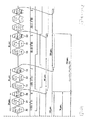
ここで、図3を参照すると、メモリユニット16は、フラッシュデバイス200およびフラッシュデバイス202を含むように示され、各フラッシュデバイスは、半導体デバイスである。前述のように、メモリユニット16は、いくつかのフラッシュメモリデバイスを含み得る。図3において、ブロック0〜ブロックNのブロックによって分けられる情報を含むように各フラッシュデバイス200および202が示されると理解されるべきであり、ブロックの各セットであるブロック0〜ブロックNは、1つのフラッシュデバイス内に含まれる。
Referring now to FIG. 3, the memory unit 16 is shown to include a
図3において、具体的には、ブロック0 210、ブロック1 212からブロックN 214のN個のブロック(Nは整数である)を含むフラッシュデバイス200が示される。同様に、具体的には、ブロック0 216、ブロック1 218からブロックN 220のN個のブロックを含むフラッシュデバイス202が示される。フラッシュデバイス200および202は、メモリ信号20を介してコントローラデバイス14(図2に示す)と通信する。データバスのDB7:0 242、制御信号(読取り、書込み、および消去のための信号を含む)240、フラッシュレディー/ビジー(Frdybsy*)バス222、フラッシュチップイネーブル0(FCE0*)信号224、およびフラッシュチップイネーブル1(FCE1*)信号226含むメモリ信号20が示される。Frdybsyバス222は、フラッシュデバイス200がプログラミングされる準備ができた時あるいはビジーである時を示すために、フラッシュレディー/ビジー0(Frdy/bsy0*)信号228と、フラッシュデバイス202がプログラミングされ得る時、およびビジーでありプログラミングされ得ない時を示すために、フラッシュレディー/ビジー1(Frdy/bsy1*)信号230とを含む。FCE0*信号224は、書込み、読取り、または消去の操作の前にフラッシュデバイス200を使用可能にするために使用される。同様に、FCE1*信号226は、書込み、読取り、または消去の操作の前にフラッシュデバイス202をイネーブルにするために使用される。メモリ信号20内に含まれる信号は、コントローラデバイス14によって展開(develop)される。本発明の一実施形態において、FCE0*信号およびFCE1*信号は、アクティブローであり、つまり、これらの状態は、低電圧または約「0」ボルトの状態の場合にアクティブになる。後者の状態の場合、これらの信号は、対応するフラッシュデバイスをアクティブにするか、またはそこへ書込む準備をする。同様に、Frdy/bsy0*信号およびFrdy/bsy1*信号がローの場合、これは、これらの信号に対応するフラッシュデバイスがビジー(または、プログラミングされているか、読取られているか、または消去されている)であることを示すのに対して、これらの信号が「ハイ」(すなわち、「ロー」電圧レベルよりも実質的に高い電位の電圧レベル)の場合、これらの信号に対応するフラッシュデバイスは、プログラミングの準備ができている。これは、これらの信号が、図3および図4の例の中に示されるよりアクティブハイ、またはその逆の極性であるように構成され得る任意の設計の選択である。
In FIG. 3, specifically, a
バスDB7:0 242は、フラッシュデバイスの中にプログラミングされるべきデータ、またはフラッシュデバイスから読取られるべきデータを結合するために使用される。バス242は、本発明の一実施形態において、8ビットのバスであり、代わりに他のビット数であってもよい。バス242は、フラッシュデバイス200および202の両方に接続されている。FCE0*信号およびFCE1*信号の状態は、他の制御信号の状態と共に、どのフラッシュデバイスデータが読取られているか、または書込まれているかを示す。例えば、FCE0*が「ロー」であり、WE*信号(図3に示されていないが、図4に示されるように制御信号240内に含まれる信号)がローである場合、フラッシュデバイス200は、バス242の上に結合されている情報を用いてプログラミングされ、バス242がフラッシュデバイス202に接続されているにも関わらず、後者は、プログラミングされない。なぜならば、後者のフラッシュイネーブル、またはFCE1*226が、「ハイ」でありアクティブでないからである。
Bus DB7: 0 242 is used to combine data to be programmed into or read from the flash device.
ユーザデータおよびECC情報(あるいは他の種類のオーバーヘッド情報)を含むセクタ情報を格納するために、16セクタ格納ロケーション232を含む、フラッシュデバイス200の各ブロック(ブロック0 210〜ブロックN 214)、およびフラッシュデバイス202の各ブロック(ブロック0 216〜ブロックN 220)が示される。別の実施形態において、ブロック(210〜214および216〜220)の各々は、16セクタ以外も含み得ると留意されるべきである。例えば、容量が128Mbitsのメモリユニットを有するシステムにおいて、各ブロックに対して32セクタが使用され得るが、64Mbitの容量を使用する場合、16セクタのブロックが必要とされる。
Each block of flash device 200 (block 0 210 to block N 214), including 16
フラッシュデバイス200および202内の同様のロケーションにある2つのブロックは、「スーパーブロック」を形成する。例えば、図3に示されるように、スーパーブロック0 204は、フラッシュデバイス200のブロック0 210およびフラッシュデバイス202のブロック0 216を含む。フラッシュデバイス200のブロック1 212およびフラッシュデバイス202のブロック1 218を含むスーパーブロック1 206が示され、フラッシュデバイス200のブロックN 214およびフラッシュデバイス202のブロックN 220を含むスーパーブロックN 208が示される。各フラッシュデバイスから1つずつの2つのブロックを含むスーパーブロックが示されるが、スーパーブロックはその代わりに、2つ以上のブロックを含み得、その場合、スーパーブロックは、各フラッシュデバイス内の同様のロケーションに位置づけられるブロックを含む。あるいは、フラッシュデバイス200のブロック0〜ブロックNおよびフラッシュデバイス202のブロック0〜ブロックNは、同じ半導体デバイス内に含まれ得る。
Two blocks at similar locations in
作動中、ホスト12(図2に示す)からのコマンドを受け取ると、フラッシュデバイス200のブロック0 210の第1のセクタ格納ロケーション232(S0)をプログラミングすることによって、セクタ情報が書込まれる。しかし、典型的に、情報の1つ以上のセクタがメモリユニット16内に格納されるため、次のセクタ情報は次いで、フラッシュデバイス202のブロック0 216の第1のセクタ格納ロケーション232(S1)内に格納される。その次のセクタ情報は、フラッシュデバイス200のブロック0の第2のセクタ格納ロケーション(S2)内に格納され、その次のセクタ情報は、フラッシュデバイス202のブロック0 216の第2のセクタ格納ロケーション(S3)内に格納されるといった具合である。従って、32セクタの情報は、スーパーブロック内に格納され得る。これによって、従来技術と比較して、ブロックのプログラミング可能な大きさは効果的に大きくなる。なぜならば、各フラッシュデバイスのブロックは、別のブロックによって続くといった具合でプログラミングされるからである。本発明の構成は、スーパーブロックへの書込み操作を達成することに関連するタスクの重複を可能にし、これは、まもなく明らかになるように、セクタ情報を書込むことに関連する時間を低減することによりシステム全体の性能を改善することによって行われる。
In operation, upon receiving a command from the host 12 (shown in FIG. 2), sector information is written by programming the first sector storage location 232 (S0) of
特定のセクタ格納ロケーションまたはブロックがプログラミングされる(または、書込まれる)場合、特定のセクタ格納ロケーションが存在するフラッシュデバイスに対応するFCE信号がイネーブルになり、フラッシュデバイスがビジーでことを示すようにFrdybsyがプログラミングされて、書込み操作が完了するまでフラッシュデバイス上のこれ以上の操作を回避する。特定のセクタ格納ロケーションに書込むために、特定のフラッシュデバイスが選択され(または、対応するFCE信号をアクティブにすることによってイネーブルにされ)、書込みコマンドは、特定のセクタ格納ロケーションが位置づけられる特定のフラッシュデバイス内のシフトレジスタ(示さず)内にシフトする。次いで、格納されるべきセクタ情報がフラッシュデバイス内にシフトし、その後、書込みコマンドが開始され、セクタ情報は、特定のフラッシュデバイス内にプログラミングされる。後者のタスクの間、すなわち、セクタ情報がフラッシュデバイス内に実際に書込まれる間、特定のフラッシュデバイスに対応するFrdybsy信号は、特定のフラッシュデバイスがビジーであることを示すようにコントローラによってプログラミングされ、このプロセスは典型的に、512バイトの大きさのセクタを完了するために200μ秒を必要とする。セクタの大きさが512であるセクタ情報を、フラッシュデバイス内にシフトすることは典型的に、30μ秒を消費する。 When a particular sector storage location or block is programmed (or written), the FCE signal corresponding to the flash device where the particular sector storage location resides is enabled to indicate that the flash device is busy Frdybsy is programmed to avoid further operations on the flash device until the write operation is complete. To write to a particular sector storage location, a particular flash device is selected (or enabled by activating the corresponding FCE signal), and the write command is sent to the particular sector storage location located Shift into a shift register (not shown) in the flash device. The sector information to be stored is then shifted into the flash device, after which a write command is initiated and the sector information is programmed into the specific flash device. During the latter task, that is, while sector information is actually written into the flash device, the Frydysy signal corresponding to a particular flash device is programmed by the controller to indicate that the particular flash device is busy. This process typically requires 200 microseconds to complete a 512 byte sector. Shifting sector information with a sector size of 512 into the flash device typically consumes 30 microseconds.
ここで図4を参照すると、フラッシュデバイス200および202をプログラミングする(または、それらに書込む)ためのイベントのシーケンスを反映するタイミング図表が示される。詳細には、Frdy/bsy0*信号228、Frdy/bsy1*信号230、FCE0*信号224、FCE1*信号226、およびWE*信号の状態に関して、S0およびS1、S2、S3、S4およびS5の6セクタのプログラミングが示され、後者は、制御信号240(図3に示す)内に含まれる。まもなく明らかになるように、フラッシュデバイスの内の1つのプログラミングは、他のフラッシュデバイス内へのセクタ情報のシフトと同時に実行されて、書込み操作の性能と比較してシフト操作を時間的に見えなく(transparent−in−time)し、従って、1つのデータバスを使用して同時に2セクタを書込む操作の速度を早くする。これによって、2セクタをプログラミングすることに関連するタスクのパイプライン処理を効果的に導入し、従って、セクタ情報の書込み操作時間を低減する。
Referring now to FIG. 4, a timing diagram reflecting a sequence of events for programming (or writing to)
バス242は、さまざまな時に異なる情報と結合され、このような情報は、図4の上部の関連する部分に示される。図4の左側から見ると、300において示されるように、バス242は、セクタS0のコマンドおよびアドレスの情報を運び、この情報は、フラッシュデバイス200内にシフトされる。この場合のコマンドは、通常、ホストによって開始される書込みコマンドである。アドレス情報は、セクタ情報がプログラミングされるべき特定のセクタのアドレス(この場合、セクタS0のアドレス)である。コマンド/アドレス情報をシフトする間、その情報の各ビットは、フラッシュデバイス200内にシリアルにシフトされる。WE*信号が生じて「ロー」状態に変わると、情報のビットがシフトされる。その間に、FCE0*信号224は、ローに保たれて、シフトするためのフラッシュデバイス200を選択する。302において、セクタ情報(特に、典型的に512バイトのユーザデータ)、エラー訂正コード(ECC)情報、および潜在的に他のセクタオーバーヘッド情報は、一度に8ビットずつ、フラッシュデバイス200内のS0にシフトされる。この場合も、WE*のローに変わるパルスのシリーズは、フラッシュデバイス200内へのセクタ情報のシフトを達成し、FCE0*信号224は、フラッシュデバイス200をイネーブルにするために「ロー」のままである。
The
304において、書込みコマンドが開始され、WE*信号が生じるとロー状態からハイ状態に変わり、FCE0*信号224はハイ状態に変わり、Frdy/bsy0*信号228はロー状態に変わる。従って、フラッシュデバイス200内へのセクタ情報の実際のプログラミング(または、書込み)が開始される。このプログラミングは、S0セクタ情報のものであり、S0セクタ情報は、図3におけるフラッシュデバイス200のブロック0の第1のセクタである。発明者の経験により、512バイトのセクタユーザデータおよび12バイトのECC情報のプログラミングに必要な時間は約200μ秒であり、シフト操作および書込みコマンドの開始操作は、約30μ秒を消費する。セクタ情報がフラッシュデバイス内にシフトされる場合、セクタ情報はまだプログラミングされておらず、むしろ、セクタ情報は、一時的保持レジスタ内に配置され、そこでプログラミングを待つが、セクタ情報がフラッシュデバイスに書き込まれる場合、後者の場合のセルは実際にプログラミングされる。さらに、フラッシュデバイスのプログラミングは、対応するFrdy/bsy*信号が「ロー」状態の場合に行われる。
At 304, when a write command is initiated and a WE * signal occurs, the low state changes to a high state, the FCE0 * signal 224 changes to a high state, and the Frdy / bsy0 * signal 228 changes to a low state. Accordingly, actual programming (or writing) of sector information into the
書込み開始操作の最後である304において、FCE0*信号224は、コントローラデバイス14によって「ハイ」状態にされて、フラッシュデバイスに書込まれている現在のセクタ情報の前に任意の新しいセクタ情報がシフトすることを防止する。フラッシュデバイス200が書込まれている間、FCE1*信号226は、306においてロー状態にされ、WE*パルスシリーズの生成によって、コマンドおよびアドレスの情報は、フラッシュデバイス202内のセクタS1にシリアルにシフトされる。次いで、308において、セクタ情報、すなわち512バイトのユーザデータおよび12バイトのECCは、WE*パルスシリーズの生成によって、フラッシュデバイス202内にシフトされる。FCE1*信号226は、このシフトプロセスのために、ローのままである。S1のシフト操作および書込みコマンドの開始操作(310)もまた、約30μ秒を消費する。S1セクタ情報のシフトは、フラッシュデバイス200のセクタS0内にセクタ情報がプログラミングされる間に行われると留意することは重要である。基本的に、これによって、30μ秒のシフト時間を見えなくする。なぜならば、セクタ情報のシフトが、別のフラッシュデバイス内へのセクタ情報の書込みと平行してかまたは同時に行われるからである。従って、本発明において、32セクタを有するスーパーブロックへの書込みは、最初の2セクタをプログラミングするために、30+30+200μ秒すなわち260μ秒を消費し、その後、最初のシフトの後にセクタの1つをシフトする時間は常に見えないので、230μ秒のみを消費する。当業者に理解されるように、本発明によって、書込み操作時間は、データバスを2倍にする必要がなく、従ってコントローラデバイスにピンカウントを追加する必要なく、低減される。つまり、本発明において、8ビットのデータバスが使用される。一方で、書込み操作時間に関して従来技術が提供する最善のシナリオは、16ビットのデータバスを必要とする。さらに、本発明において、スーパーブロックは、2つより多くのブロックまたは32セクタを含み得、この場合も同様に、データバスに関する必要なピンの数は同じままであり、書き込み操作時間の改善も同じままである。つまり、従来技術において、2セクタの書込み操作時間が230μ秒を得るために、32ビットのデータバスが必要であるが、データバスのピンカウントを8ビットより多くに増加させる必要なく、本発明によって同じ書込み操作時間が達成される。実際、各スーパーブロックに対するブロックの数が増加し、より多くのフラッシュデバイスが並列にプログラミングされるにつれて、本発明による利点は増大する。十分なフラッシュデバイスが並列に配置されると、必要とされる余分なデータバスピンを配置する十分な空間がなくなるので、余分なデータバスラインを使用する従来技術システムの方法および技術は非実用的になる。
At 304, the end of the write start operation, the FCE0 * signal 224 is brought "high" by the
いくつかの従来技術の手法において、30+30+200+200μ秒または460μ秒の書込み時間が必要であり、上記において十分に説明されたような、230μ秒が達成され得る特定の他の従来技術において、本発明の待ち時間をはるかに越える待ち時間の遅れがあり、その結果、前者による書込み性能を低減する。繰り返して言うと、後者の従来技術の手法は、各ブロックの書込み操作の前に、ブロックのセクタが、バッファ内に格納されることを必要とする。ブロックが32セクタである場合、4セクタをプログラミングすることを想定して、全4セクタがバッファ内に格納される必要があり、これは、バッファの大きさが、本発明が必要とする大きさより大きいことを必要とし、その結果、従来技術のシステムの製造コストを増加させる。さもなければ、情報の2セクタのみがバッファ内に格納される場合、後者のプログラミングが開始され得る前に、ホストが次の2セクタをバッファ内に提供し、コントローラがそれらをバッファ内に格納するのを待たなければならないことに関連する実質的な遅れがある。これによって、2セクタの書込み操作に関連する時間を230μ秒以上に実質的に長くする。これは、部分的に、従来技術の方法および装置が、セクタ(コマンド、アドレス、データ、およびECC)のシフト時間を隠すことができないからである。 In some prior art approaches, a write time of 30 + 30 + 200 + 200 μs or 460 μs is required, and in certain other prior art where 230 μs can be achieved, as fully explained above, There is a latency delay that goes far beyond time, resulting in reduced write performance by the former. To reiterate, the latter prior art approach requires that the sectors of the block be stored in a buffer before each block write operation. If the block is 32 sectors, assuming that 4 sectors are programmed, all 4 sectors need to be stored in the buffer, because the size of the buffer is larger than required by the present invention. It needs to be large, and as a result, increases the manufacturing cost of prior art systems. Otherwise, if only two sectors of information are stored in the buffer, the host provides the next two sectors in the buffer before the latter programming can begin and the controller stores them in the buffer There is a substantial delay associated with having to wait for. This substantially increases the time associated with a two-sector write operation to more than 230 μsec. This is partly because prior art methods and devices cannot hide the shift times of sectors (commands, addresses, data, and ECC).
引き続き、図4を参照すると、310において、S1の書込みコマンドが開始されることによって、WE*信号がローに変わる。WE*信号がまたハイに変わることによって、Frdy/bsy1*230がローに変えられて、その結果、フラッシュデバイス202のセクタS1内へのセクタ情報のプログラミングが開始される。この場合も同様に、後者のプロセスは、512バイトのセクタに対して200μ秒を消費する。Frdy/bsy1*は、約200μ秒の間、ローのままである。従って、セクタS0およびS1に書込むためのプログラミング時間の総計は、230μ秒である。余分な30μ秒が、第1のセクタ情報のシフトに関連するので、最初の2セクタ(この場合、セクタS0およびS1)のシフトおよびプログラミングが必要とするのは、260μ秒のみである。それ以降、2セクタのシフトおよびプログラミングは、230μ秒のみを必要とする。なぜならば、まもなく明らかになるように、セクタの1つをシフトすることが、もう1つのセクタの書込み時間内に隠されているからである。最初の印象では、最初の2セクタの書込み操作時間、すなわち260μ秒は、上記で説明されたいくつかの従来技術のシステムのいくつかに関連する書込み操作時間よりも長く見えるが、実際には、本発明の使用により、プログラミングは全体的に低減する。これは、シフトおよび書込みの時間が開始される前にバッファ内に格納するために、コントローラと同時にプログラミングされるべきセクタをホストに送らせるという従来技術システムの要件が原因である。従って、ホストが上記を完了する間、書込みプロセスは保留となり、通常、ホスト書込み操作が遅いことは公知であり、従って、セクタのプログラミング全体に関連する時間は増加する。しかし、本発明において、初めて2セクタが書込まれる場合を除いて、任意の2セクタの書込みを開始する前に、ホストが予め必要な数のセクタを提供するのを待つ必要はない。つまり、最初は、ホストは、バッファ内への格納のために、コントローラに情報の2セクタを提供する必要がある。それ以降、ホストは、他のセクタがプログラミングされている間にセクタ情報を提供し得る。高速ホストを使用するシステムにおいて、本発明と従来技術との間のこの差は、強調される効果を有さないかもしれないと留意されるべきである。しかし、コスト制限が部分的な原因となって通常は、より遅いホストが使用される。このようなシステムにおいて、この差は、よく留意されている。
Continuing to refer to FIG. 4, at 310, the WE * signal changes to low due to the start of the S1 write command. By changing the WE * signal to high again, Frdy /
図4において、312、314、および316において、セクタS2について行われるということを除いて、上記で説明された方法とほとんど同じ方法によって、コマンドおよびアドレスの情報がフラッシュデバイス200内にシリアルにシフトされ、セクタ情報がフラッシュデバイス200内にシフトされて、書込みコマンドが開始される。図3において、フラッシュデバイス200のブロック0内の第2のセクタとして、S2が示される。314におけるセクタ情報のシフトは、フラッシュデバイス202のセクタS1内にセクタ情報を書き込む間に行われる。この場合も同様に、これによって、セクタ情報のシフトに関連する時間が隠されて、従って、このセクタの書込み時間を約30μ秒だけ低減させる。より大きなセクタ(512バイトよりも大きなセクタ)に関して、時間がさらに短縮される。
In FIG. 4, command and address information is serially shifted into
316において書込みコマンドの開始を完了し、WE*信号がローからハイに変わると、Frdy/bsy0*信号228がロー状態に変えられ、その後の約200μ秒の間にセクタ情報がフラッシュデバイス200内にプログラミングされるように、S2セクタ内へのセクタ情報のプログラミングが開始される。次いで、318において、セクタS3のコマンドおよびアドレスの情報が、フラッシュデバイス202内にシリアルにシフトされる。320において、セクタ情報は、フラッシュデバイス202内にシフトされる。前述のように、これらのシフト操作は、S2セクタ内へのセクタ情報の書込みと共に起こり、セクタ情報、コマンド、およびアドレスのシフトに関連する時間が、書込み操作の全体に対して、隠されるか、または見えなくされる。従って、プロセスは、プログラミングされるようにホストによって命令されたすべてのセクタが、そのようにプログラミングされるまで続く。プロセスは、セクタS4およびS5についても、同じ方法で続けられる。
When the start of the write command is completed at 316 and the WE * signal changes from low to high, the Frdy / bsy0 * signal 228 is changed to a low state, and sector information is stored in the
本発明において、ホストが1つのセクタのセクタ情報を提供し、そのセクタ情報がバッファ内に格納されるとすぐに、コントローラ14がセクタ書込み操作を開始すると理解される。従って、従来技術のシステムが必要とするように、書込み操作が開始される前に、情報の2つ以上のセクタがホストから送られてくるのを待つ必要はない。従って、書込みの前に、ホストが2つ以上のセクタ情報を提供するのを待つことによって生じる遅れは、本発明によって低減される。
In the present invention, it is understood that the
図5は、本発明の別の実施形態のタイミング図を示し、ここで、全てのフラッシュデバイスに対して1つのFrdy/bsy*信号が使用される。さらに、本発明の別の局面において、セクタをプログラミングする際の、1つ以上のエラーの発生を知らせるために割り込み信号が使用される。後者の場合、フラッシュセルのプログラミングに関連する感度が原因となり、通常、読取り照合(read−verify)操作は、セクタのプログラミングが成功したことを確定するために、セクタがプログラミングされる度に実行されると理解されるべきである。従来技術のシステムにおいて、割り込み信号が使用されないため、セクタの書込み操作が完了した後、プログラミングされていたセクタを含むフラッシュデバイスは、フラッシュデバイスをプログラミングする際にエラーが生じたかどうかを判定するためにポーリングされる必要がある。これは、書込み操作全体に対する追加の工程であり、割り込み信号の使用によって、基本的に消去される。 FIG. 5 shows a timing diagram of another embodiment of the present invention, where one Frdy / bsy * signal is used for all flash devices. Furthermore, in another aspect of the invention, an interrupt signal is used to signal the occurrence of one or more errors when programming a sector. In the latter case, due to the sensitivity associated with flash cell programming, a read-verify operation is usually performed each time a sector is programmed to determine that the sector has been successfully programmed. Should be understood. In prior art systems, since no interrupt signal is used, after the sector write operation is complete, the flash device containing the programmed sector is used to determine if an error has occurred in programming the flash device. Need to be polled. This is an additional step for the entire write operation and is basically erased by the use of an interrupt signal.
図5において、Frdy/Bsy0*信号227のタイミングが示される。この信号は、複数のFrdy/Bsy信号(各フラッシュデバイスに対して1つ)の使用に取って代わり、全てのフラッシュデバイスによって共有される。従って、信号227は、第1のセクタ、すなわちS0のステア書込みコマンド(stare write command)504の後にローに変わり、フラッシュデバイスがプログラミングされている間中、ローのままである。前述の実施形態のように、プログラミングされているセクタの内の1つのセクタ情報をシフトすることは、他のセクタをプログラミングしている間に行われる。しかし、他のFrdy/bsy*信号が使用されないため、信号227は、全てのセクタをプログラミングする間中、ローのままであり、これは、図4に関して説明した時間と同じ時間、すなわち、2セクタをプログラミングするための230μ秒、および最初の2セクタをプログラミングするための260μ秒だけかかる。
In FIG. 5, the timing of the Frdy / Bsy0 * signal 227 is shown. This signal replaces the use of multiple Frdy / Bsy signals (one for each flash device) and is shared by all flash devices. Thus, signal 227 turns low after the first sector, the S0
INTQ*信号229がフラッシュデバイスによって展開される。信号229は、メモリユニット16(図2に示す)の全てのフラッシュデバイスに接続されているオープンコレクタ信号である。任意のフラッシュメモリデバイスによってエラーが検出される場合、すなわち、プログラミングされたセクタ情報とプログラミングされるはずだったセクタ情報との間に不一致がある場合、信号229は、アクティブ状態にされ(この場合、アクティブ状態は論理「ロー」である)、コントローラデバイス14への入力として機能して、フラッシュデバイスをプログラミング中に生じ得た任意のエラーを後者に知らせる。従来技術のシステムにおいて、前述のように、セクタがプログラミングされた後は毎回、正確を期して、プログラミングされたセクタを含むフラッシュデバイスをチェックする。これは、所定のステータスレジスタの状態をチェックすることにより行われる。
An INTQ * signal 229 is developed by the flash device.
実際、フラッシュデバイスは、読取り照合操作を実行し、ここで、セクタ内でプログラミングされた情報が読み返され、その後、読取りステータス(read
status)コマンドがコントローラによって実行される。この読取り情報が、プログラミングされたものと一致しない場合、エラーが検出される。従来技術のシステムにおいて、書込み操作のステータスは、読取りステータス操作中にステータスレジスタをチェックすることによりポーリングされて、各セクタ書込み操作の後、セクタをプログラミングする際に問題があったかどうかを判定する(これらの時間は図5に示す)。しかし、本発明の一実施形態によって、INTQ*信号229は、ステータス情報をポーリングする必要性を消去する。なぜならば、読取り照合操作が、読取りセクタとプログラミングされるはずだったセクタとの間の不一致を報告する場合、信号299がアクティブになって、コントローラにエラーを知らせるからである。この点において、本発明の一実施形態は、マイクロプロセッサ24(図2に示す)によって実行されるタスクを減少させる。なぜならば、従来技術のシステムにおいて、プログラミングエラーを見つけるために、マイクロプロセッサがステータスレジスタをチェックするからである。従って、本発明は、マイクロプロセッサを他の機能に貢献可能にすることにより、システムの全体的な性能を効果的に改善する。
In fact, the flash device performs a read verification operation where information programmed in the sector is read back and then read status (read
status) command is executed by the controller. If this read information does not match the programmed one, an error is detected. In prior art systems, the status of write operations is polled by checking the status register during read status operations to determine if there was a problem programming the sector after each sector write operation (these Is shown in FIG. However, according to one embodiment of the invention, the INTQ * signal 229 eliminates the need to poll status information. This is because if the read verification operation reports a discrepancy between the read sector and the sector that was to be programmed, signal 299 is activated to inform the controller of the error. In this regard, one embodiment of the present invention reduces the tasks performed by the microprocessor 24 (shown in FIG. 2). This is because, in prior art systems, the microprocessor checks the status register to find programming errors. Thus, the present invention effectively improves the overall performance of the system by allowing the microprocessor to contribute to other functions.
本発明は、特定の実施形態に関して説明されたが、当業者に本発明の改変および変更がおそらく明らかであることが予想される。従って、下記の請求の範囲は、本発明の真の精神および範囲内にあるような改変および変更を全て含むと解釈されることを意図する。 Although the present invention has been described with respect to particular embodiments, modifications and alterations of the present invention will likely be apparent to those skilled in the art. Accordingly, the following claims are intended to be construed to include all such modifications and changes as fall within the true spirit and scope of this invention.
Claims (7)
該不揮発性メモリシステムは、 The nonvolatile memory system includes:
特定のスーパーブロックの第1のブロックの第1のセクタにセクタ情報をシフトさせるコントローラであって、該コントローラはさらに、該特定のスーパーブロックの第2のブロックの第1のセクタにセクタ情報をシフトさせ、該特定のスーパーブロックの該第1のブロックの該第1のセクタにセクタ情報を書き込む、コントローラを備え、 A controller that shifts sector information to a first sector of a first block of a particular superblock, the controller further shifting sector information to a first sector of a second block of the particular superblock And writing a sector information to the first sector of the first block of the particular superblock,
該第1のブロックの該第1のセクタへの書込み中に、該第2のブロックの該第1のセクタへのシフト全体が起き、 During the writing of the first block to the first sector, the entire shift of the second block to the first sector occurs;
該第1のブロックの該第1のセクタおよび該第2のブロックの該第1のセクタに対するセクタ情報のシフトは、該ホストが該セクタ情報を提供した直後に起きる、不揮発性メモリシステム。 A non-volatile memory system, wherein the shifting of sector information for the first sector of the first block and the first sector of the second block occurs immediately after the host provides the sector information.
該方法は、 The method
特定のスーパーブロックの第1のブロックの第1のセクタにセクタ情報をシフトさせることと、 Shifting the sector information to the first sector of the first block of a particular superblock;
該特定のスーパーブロックの第2のブロックの第1のセクタにセクタ情報をシフトさせることと、 Shifting sector information to the first sector of the second block of the particular superblock;
該特定のスーパーブロックの該第1のブロックの該第1のセクタにセクタ情報を書き込むことであって、該第1のブロックの該第1のセクタへの書込み中に、該第2のブロックへとシフトさせるステップ全体が起きる、ことと Writing sector information to the first sector of the first block of the particular superblock to the second block during the writing of the first block to the first sector And the whole step of shifting happens
を含み、該第1のブロックの該第1のセクタおよび該第2のブロックの該第1のセクタに対するセクタ情報のシフトは、該ホストが該セクタ情報を提供した直後に起きる、方法。 And the shifting of sector information for the first sector of the first block and the first sector of the second block occurs immediately after the host provides the sector information.
該不揮発性メモリシステムは、 The nonvolatile memory system includes:
特定のスーパーブロックにセクタ情報を書き込むコントローラであって、該セクタ情報の書込みが成功したか否かを示す、該不揮発性メモリからの割込み信号に応答するコントローラを備え、 A controller for writing sector information to a specific superblock, the controller responding to an interrupt signal from the non-volatile memory indicating whether or not the writing of the sector information was successful;
該割込み信号が、ステータス情報のポーリングを回避し、それにより、セクタ情報の書込みを行うことに関連する時間を減少させ、 The interrupt signal avoids polling of status information, thereby reducing the time associated with writing sector information;
該コントローラがさらに、特定のスーパーブロックの第1のブロックの第1のセクタにセクタ情報をシフトさせ、該コントローラがさらに、該特定のスーパーブロックの第2のブロックの第1のセクタにセクタ情報をシフトさせ、該特定のスーパーブロックの該第1のブロックの該第1のセクタにセクタ情報を書き込み、該第1のブロックの該第1のセクタへの書込み中に、該第2のブロックの該第1のセクタへのシフト全体が起き、該第1のブロックの該第1のセクタおよび該第2のブロックの該第1のセクタに対するセクタ情報のシフトは、該ホストが該セクタ情報を提供した直後に起きる、不揮発性メモリシステム。 The controller further shifts the sector information to the first sector of the first block of the specific superblock, and the controller further transfers the sector information to the first sector of the second block of the specific superblock. Shifting, writing sector information to the first sector of the first block of the particular superblock, and writing the first block to the first sector of the second block The entire shift to the first sector occurred and the shift of the sector information for the first sector of the first block and the first sector of the second block caused the host to provide the sector information A non-volatile memory system that occurs immediately after.
Applications Claiming Priority (1)
| Application Number | Priority Date | Filing Date | Title |
|---|---|---|---|
| US09/389,994 US6141249A (en) | 1999-04-01 | 1999-09-03 | Organization of blocks within a nonvolatile memory unit to effectively decrease sector write operation time |
Related Parent Applications (1)
| Application Number | Title | Priority Date | Filing Date |
|---|---|---|---|
| JP2001522164A Division JP2003508861A (en) | 1999-09-03 | 2000-08-25 | Block configuration in a non-volatile memory unit for effectively reducing sector write operation time |
Publications (1)
| Publication Number | Publication Date |
|---|---|
| JP2010152913A true JP2010152913A (en) | 2010-07-08 |
Family
ID=23540599
Family Applications (2)
| Application Number | Title | Priority Date | Filing Date |
|---|---|---|---|
| JP2001522164A Pending JP2003508861A (en) | 1999-09-03 | 2000-08-25 | Block configuration in a non-volatile memory unit for effectively reducing sector write operation time |
| JP2010031847A Pending JP2010152913A (en) | 1999-09-03 | 2010-02-16 | Organization of blocks within nonvolatile memory unit to effectively decrease sector write operation time |
Family Applications Before (1)
| Application Number | Title | Priority Date | Filing Date |
|---|---|---|---|
| JP2001522164A Pending JP2003508861A (en) | 1999-09-03 | 2000-08-25 | Block configuration in a non-volatile memory unit for effectively reducing sector write operation time |
Country Status (7)
| Country | Link |
|---|---|
| US (1) | US6141249A (en) |
| EP (1) | EP1242868B1 (en) |
| JP (2) | JP2003508861A (en) |
| AT (1) | ATE410727T1 (en) |
| AU (1) | AU6942100A (en) |
| DE (1) | DE60040484D1 (en) |
| WO (1) | WO2001018640A1 (en) |
Cited By (1)
| Publication number | Priority date | Publication date | Assignee | Title |
|---|---|---|---|---|
| JP2012519899A (en) * | 2009-03-04 | 2012-08-30 | マイクロン テクノロジー, インク. | Select memory block |
Families Citing this family (78)
| Publication number | Priority date | Publication date | Assignee | Title |
|---|---|---|---|---|
| US5845313A (en) | 1995-07-31 | 1998-12-01 | Lexar | Direct logical block addressing flash memory mass storage architecture |
| US8171203B2 (en) | 1995-07-31 | 2012-05-01 | Micron Technology, Inc. | Faster write operations to nonvolatile memory using FSInfo sector manipulation |
| US6728851B1 (en) | 1995-07-31 | 2004-04-27 | Lexar Media, Inc. | Increasing the memory performance of flash memory devices by writing sectors simultaneously to multiple flash memory devices |
| US6978342B1 (en) | 1995-07-31 | 2005-12-20 | Lexar Media, Inc. | Moving sectors within a block of information in a flash memory mass storage architecture |
| JP3714969B2 (en) | 1998-03-02 | 2005-11-09 | レクサー・メディア・インコーポレイテッド | Flash memory card with improved operating mode detection and user-friendly interfacing system |
| KR100544175B1 (en) * | 1999-05-08 | 2006-01-23 | 삼성전자주식회사 | Recording medium storing linking type information and method for processing defective area |
| US6606628B1 (en) * | 2000-02-14 | 2003-08-12 | Cisco Technology, Inc. | File system for nonvolatile memory |
| US6426893B1 (en) | 2000-02-17 | 2002-07-30 | Sandisk Corporation | Flash eeprom system with simultaneous multiple data sector programming and storage of physical block characteristics in other designated blocks |
| US7167944B1 (en) | 2000-07-21 | 2007-01-23 | Lexar Media, Inc. | Block management for mass storage |
| US7155559B1 (en) | 2000-08-25 | 2006-12-26 | Lexar Media, Inc. | Flash memory architecture with separate storage of overhead and user data |
| US6772274B1 (en) | 2000-09-13 | 2004-08-03 | Lexar Media, Inc. | Flash memory system and method implementing LBA to PBA correlation within flash memory array |
| JP4059473B2 (en) * | 2001-08-09 | 2008-03-12 | 株式会社ルネサステクノロジ | Memory card and memory controller |
| GB0123421D0 (en) | 2001-09-28 | 2001-11-21 | Memquest Ltd | Power management system |
| GB0123410D0 (en) | 2001-09-28 | 2001-11-21 | Memquest Ltd | Memory system for data storage and retrieval |
| GB0123416D0 (en) | 2001-09-28 | 2001-11-21 | Memquest Ltd | Non-volatile memory control |
| GB0123415D0 (en) | 2001-09-28 | 2001-11-21 | Memquest Ltd | Method of writing data to non-volatile memory |
| WO2003060722A1 (en) * | 2002-01-09 | 2003-07-24 | Renesas Technology Corp. | Memory system and memory card |
| TWI240861B (en) * | 2002-01-11 | 2005-10-01 | Integrated Circuit Solution In | Data access method and architecture of flash memory |
| US7246268B2 (en) * | 2002-01-16 | 2007-07-17 | Sandisk Corporation | Method and apparatus for dynamic degradation detection |
| US6732222B1 (en) * | 2002-02-01 | 2004-05-04 | Silicon Motion, Inc. | Method for performing flash memory file management |
| US6839826B2 (en) * | 2002-02-06 | 2005-01-04 | Sandisk Corporation | Memory device with pointer structure to map logical to physical addresses |
| US7231643B1 (en) | 2002-02-22 | 2007-06-12 | Lexar Media, Inc. | Image rescue system including direct communication between an application program and a device driver |
| WO2003071853A2 (en) * | 2002-02-22 | 2003-09-04 | Lexar Media, Inc. | Removable memory media with integral indicator light |
| DE10256509B4 (en) * | 2002-06-19 | 2008-06-12 | Hyperstone Gmbh | Method for addressing block-by-block erasable memories |
| KR101087906B1 (en) * | 2003-11-18 | 2011-11-30 | 파나소닉 주식회사 | File recording device |
| US20050138464A1 (en) * | 2003-11-21 | 2005-06-23 | Chong Pohsoon | Scratch fill using scratch tracking table |
| US7139864B2 (en) * | 2003-12-30 | 2006-11-21 | Sandisk Corporation | Non-volatile memory and method with block management system |
| US20050144363A1 (en) * | 2003-12-30 | 2005-06-30 | Sinclair Alan W. | Data boundary management |
| US7433993B2 (en) * | 2003-12-30 | 2008-10-07 | San Disk Corportion | Adaptive metablocks |
| US7383375B2 (en) * | 2003-12-30 | 2008-06-03 | Sandisk Corporation | Data run programming |
| CN100433195C (en) * | 2003-12-31 | 2008-11-12 | 深圳市朗科科技股份有限公司 | Flash memory medium data writing method |
| JP2005222315A (en) | 2004-02-05 | 2005-08-18 | Sony Corp | Nonvolatile memory control method and unit |
| US7725628B1 (en) | 2004-04-20 | 2010-05-25 | Lexar Media, Inc. | Direct secondary device interface by a host |
| US7370166B1 (en) | 2004-04-30 | 2008-05-06 | Lexar Media, Inc. | Secure portable storage device |
| US7464306B1 (en) | 2004-08-27 | 2008-12-09 | Lexar Media, Inc. | Status of overall health of nonvolatile memory |
| US7594063B1 (en) | 2004-08-27 | 2009-09-22 | Lexar Media, Inc. | Storage capacity status |
| KR100621631B1 (en) * | 2005-01-11 | 2006-09-13 | 삼성전자주식회사 | Solid state disk controller apparatus |
| US7509471B2 (en) * | 2005-10-27 | 2009-03-24 | Sandisk Corporation | Methods for adaptively handling data writes in non-volatile memories |
| US7631162B2 (en) | 2005-10-27 | 2009-12-08 | Sandisck Corporation | Non-volatile memory with adaptive handling of data writes |
| US8069318B2 (en) * | 2005-12-01 | 2011-11-29 | Urenschi Assets Limited Liability Company | High performance data rate system for flash devices |
| US7606992B1 (en) * | 2005-12-01 | 2009-10-20 | Chris Karabatsos | High performance data rate system for flash devices |
| WO2007066720A1 (en) * | 2005-12-09 | 2007-06-14 | Matsushita Electric Industrial Co., Ltd. | Nonvolatile memory device, method of writing data, and method of reading out data |
| US7739576B2 (en) * | 2006-08-31 | 2010-06-15 | Micron Technology, Inc. | Variable strength ECC |
| KR100868674B1 (en) | 2006-10-30 | 2008-11-13 | 한국과학기술원 | The method of managing flash memory |
| US8489817B2 (en) | 2007-12-06 | 2013-07-16 | Fusion-Io, Inc. | Apparatus, system, and method for caching data |
| US8443134B2 (en) * | 2006-12-06 | 2013-05-14 | Fusion-Io, Inc. | Apparatus, system, and method for graceful cache device degradation |
| CA2672100A1 (en) * | 2006-12-06 | 2008-06-12 | Fusion Multisystems, Inc. | Apparatus, system, and method for solid-state storage as cache for high-capacity, non-volatile storage |
| US8706968B2 (en) * | 2007-12-06 | 2014-04-22 | Fusion-Io, Inc. | Apparatus, system, and method for redundant write caching |
| US9495241B2 (en) | 2006-12-06 | 2016-11-15 | Longitude Enterprise Flash S.A.R.L. | Systems and methods for adaptive data storage |
| US9116823B2 (en) | 2006-12-06 | 2015-08-25 | Intelligent Intellectual Property Holdings 2 Llc | Systems and methods for adaptive error-correction coding |
| US9104599B2 (en) | 2007-12-06 | 2015-08-11 | Intelligent Intellectual Property Holdings 2 Llc | Apparatus, system, and method for destaging cached data |
| US8122322B2 (en) | 2007-07-31 | 2012-02-21 | Seagate Technology Llc | System and method of storing reliability data |
| US8316277B2 (en) * | 2007-12-06 | 2012-11-20 | Fusion-Io, Inc. | Apparatus, system, and method for ensuring data validity in a data storage process |
| US7836226B2 (en) | 2007-12-06 | 2010-11-16 | Fusion-Io, Inc. | Apparatus, system, and method for coordinating storage requests in a multi-processor/multi-thread environment |
| US9519540B2 (en) | 2007-12-06 | 2016-12-13 | Sandisk Technologies Llc | Apparatus, system, and method for destaging cached data |
| US7966445B2 (en) * | 2007-12-24 | 2011-06-21 | Telefonaktiebolaget L M Ericsson (Publ) | Read status controller |
| US7979264B2 (en) * | 2008-02-26 | 2011-07-12 | Streaming Networks (Pvt) Ltd | System and method for interfacing a media processing apparatus with a computer |
| US8180995B2 (en) | 2009-01-21 | 2012-05-15 | Micron Technology, Inc. | Logical address offset in response to detecting a memory formatting operation |
| US8095765B2 (en) * | 2009-03-04 | 2012-01-10 | Micron Technology, Inc. | Memory block management |
| KR101717644B1 (en) | 2009-09-08 | 2017-03-27 | 샌디스크 테크놀로지스 엘엘씨 | Apparatus, system, and method for caching data on a solid-state storage device |
| KR101796116B1 (en) | 2010-10-20 | 2017-11-10 | 삼성전자 주식회사 | Semiconductor device, memory module and memory system having the same and operating method thereof |
| US8966184B2 (en) | 2011-01-31 | 2015-02-24 | Intelligent Intellectual Property Holdings 2, LLC. | Apparatus, system, and method for managing eviction of data |
| US8874823B2 (en) | 2011-02-15 | 2014-10-28 | Intellectual Property Holdings 2 Llc | Systems and methods for managing data input/output operations |
| US9003104B2 (en) | 2011-02-15 | 2015-04-07 | Intelligent Intellectual Property Holdings 2 Llc | Systems and methods for a file-level cache |
| US9201677B2 (en) | 2011-05-23 | 2015-12-01 | Intelligent Intellectual Property Holdings 2 Llc | Managing data input/output operations |
| US9141527B2 (en) | 2011-02-25 | 2015-09-22 | Intelligent Intellectual Property Holdings 2 Llc | Managing cache pools |
| US10102117B2 (en) | 2012-01-12 | 2018-10-16 | Sandisk Technologies Llc | Systems and methods for cache and storage device coordination |
| US9767032B2 (en) | 2012-01-12 | 2017-09-19 | Sandisk Technologies Llc | Systems and methods for cache endurance |
| US9251052B2 (en) | 2012-01-12 | 2016-02-02 | Intelligent Intellectual Property Holdings 2 Llc | Systems and methods for profiling a non-volatile cache having a logical-to-physical translation layer |
| US9251086B2 (en) | 2012-01-24 | 2016-02-02 | SanDisk Technologies, Inc. | Apparatus, system, and method for managing a cache |
| US9116812B2 (en) | 2012-01-27 | 2015-08-25 | Intelligent Intellectual Property Holdings 2 Llc | Systems and methods for a de-duplication cache |
| US10359972B2 (en) | 2012-08-31 | 2019-07-23 | Sandisk Technologies Llc | Systems, methods, and interfaces for adaptive persistence |
| US10019353B2 (en) | 2012-03-02 | 2018-07-10 | Longitude Enterprise Flash S.A.R.L. | Systems and methods for referencing data on a storage medium |
| US9612966B2 (en) | 2012-07-03 | 2017-04-04 | Sandisk Technologies Llc | Systems, methods and apparatus for a virtual machine cache |
| US10339056B2 (en) | 2012-07-03 | 2019-07-02 | Sandisk Technologies Llc | Systems, methods and apparatus for cache transfers |
| US9842053B2 (en) | 2013-03-15 | 2017-12-12 | Sandisk Technologies Llc | Systems and methods for persistent cache logging |
| US10114562B2 (en) | 2014-09-16 | 2018-10-30 | Sandisk Technologies Llc | Adaptive block allocation in nonvolatile memory |
| US9817593B1 (en) | 2016-07-11 | 2017-11-14 | Sandisk Technologies Llc | Block management in non-volatile memory system with non-blocking control sync system |
Citations (6)
| Publication number | Priority date | Publication date | Assignee | Title |
|---|---|---|---|---|
| JPH06332806A (en) * | 1993-05-25 | 1994-12-02 | Hitachi Ltd | Storage system with flash memory as storage medium and control method therefor |
| JPH0714392A (en) * | 1993-06-14 | 1995-01-17 | Toshiba Corp | Nonvolatile semiconductor memory and semiconductor disk device using the same |
| JPH07141258A (en) * | 1993-11-15 | 1995-06-02 | Toshiba Corp | Data recording and reproducing device |
| JPH07302176A (en) * | 1994-05-09 | 1995-11-14 | Toshiba Corp | Semiconductor disk device |
| JPH11191297A (en) * | 1997-12-26 | 1999-07-13 | Hitachi Ltd | High speed rewritable memory device using nonvolatile memory and method of rewriting data in said memory device |
| WO1999044113A2 (en) * | 1998-02-25 | 1999-09-02 | Lexar Media, Inc. | Increasing the memory performance of flash memory devices by writing sectors simultaneously to multiple flash memory devices |
Family Cites Families (85)
| Publication number | Priority date | Publication date | Assignee | Title |
|---|---|---|---|---|
| US4210959A (en) * | 1978-05-10 | 1980-07-01 | Apple Computer, Inc. | Controller for magnetic disc, recorder, or the like |
| FR2426938A1 (en) * | 1978-05-26 | 1979-12-21 | Cii Honeywell Bull | DEVICE FOR DETECTION OF DEFECTIVE SECTORS AND ALLOCATION OF REPLACEMENT SECTORS IN A DISK MEMORY |
| US4355376A (en) * | 1980-09-30 | 1982-10-19 | Burroughs Corporation | Apparatus and method for utilizing partially defective memory devices |
| JPS5764383A (en) * | 1980-10-03 | 1982-04-19 | Toshiba Corp | Address converting method and its device |
| JPS57132256A (en) * | 1981-02-09 | 1982-08-16 | Sony Corp | Memory device |
| JPS5877034A (en) * | 1981-10-30 | 1983-05-10 | Hitachi Ltd | Controlling system for unrewritable storage device |
| US4450559A (en) * | 1981-12-24 | 1984-05-22 | International Business Machines Corporation | Memory system with selective assignment of spare locations |
| JPS58215794A (en) * | 1982-06-08 | 1983-12-15 | Toshiba Corp | Non-volatile memory device |
| JPS58215795A (en) * | 1982-06-08 | 1983-12-15 | Toshiba Corp | Non-volatile memory device |
| US4498146A (en) * | 1982-07-30 | 1985-02-05 | At&T Bell Laboratories | Management of defects in storage media |
| JPS5945695A (en) * | 1982-09-07 | 1984-03-14 | Fujitsu Ltd | Ic memory |
| US4710871A (en) * | 1982-11-01 | 1987-12-01 | Ncr Corporation | Data transmitting and receiving apparatus |
| AU557723B2 (en) * | 1982-12-17 | 1987-01-08 | Blue Circle Southern Cement Ltd. | Electronic memory system |
| JPS59162695A (en) * | 1983-03-07 | 1984-09-13 | Nec Corp | Storage device |
| US4896262A (en) * | 1984-02-24 | 1990-01-23 | Kabushiki Kaisha Meidensha | Emulation device for converting magnetic disc memory mode signal from computer into semiconductor memory access mode signal for semiconductor memory |
| JPS60212900A (en) * | 1984-04-09 | 1985-10-25 | Nec Corp | Semiconductor fixed memory |
| JPS6196598A (en) * | 1984-10-17 | 1986-05-15 | Fuji Electric Co Ltd | Count data memory method of electric erasable p-rom |
| US4654847A (en) * | 1984-12-28 | 1987-03-31 | International Business Machines | Apparatus for automatically correcting erroneous data and for storing the corrected data in a common pool alternate memory array |
| JPS61208673A (en) * | 1985-03-12 | 1986-09-17 | Matsushita Electric Ind Co Ltd | Information recording and reproducing device |
| US4744062A (en) * | 1985-04-23 | 1988-05-10 | Hitachi, Ltd. | Semiconductor integrated circuit with nonvolatile memory |
| JPS62102482A (en) * | 1985-10-28 | 1987-05-12 | Matsushita Electric Ind Co Ltd | Information recording and reproducing device |
| JP2664137B2 (en) * | 1985-10-29 | 1997-10-15 | 凸版印刷株式会社 | IC card |
| US4800520A (en) * | 1985-10-29 | 1989-01-24 | Kabushiki Kaisha Toshiba | Portable electronic device with garbage collection function |
| US4924331A (en) * | 1985-11-20 | 1990-05-08 | Seagate Technology, Inc. | Method for mapping around defective sectors in a disc drive |
| US4746998A (en) * | 1985-11-20 | 1988-05-24 | Seagate Technology, Inc. | Method for mapping around defective sectors in a disc drive |
| US4757474A (en) * | 1986-01-28 | 1988-07-12 | Fujitsu Limited | Semiconductor memory device having redundancy circuit portion |
| JPH07109717B2 (en) * | 1986-05-31 | 1995-11-22 | キヤノン株式会社 | Memory write control method |
| JP2685173B2 (en) * | 1986-05-31 | 1997-12-03 | キヤノン株式会社 | Memory write control method |
| US4953122A (en) * | 1986-10-31 | 1990-08-28 | Laserdrive Ltd. | Pseudo-erasable and rewritable write-once optical disk memory system |
| JPS63183700A (en) * | 1987-01-26 | 1988-07-29 | Mitsubishi Electric Corp | Eeprom access method |
| US5268870A (en) * | 1988-06-08 | 1993-12-07 | Eliyahou Harari | Flash EEPROM system and intelligent programming and erasing methods therefor |
| US5293560A (en) * | 1988-06-08 | 1994-03-08 | Eliyahou Harari | Multi-state flash EEPROM system using incremental programing and erasing methods |
| US5268319A (en) * | 1988-06-08 | 1993-12-07 | Eliyahou Harari | Highly compact EPROM and flash EEPROM devices |
| US5168465A (en) * | 1988-06-08 | 1992-12-01 | Eliyahou Harari | Highly compact EPROM and flash EEPROM devices |
| US5198380A (en) * | 1988-06-08 | 1993-03-30 | Sundisk Corporation | Method of highly compact EPROM and flash EEPROM devices |
| US5268318A (en) * | 1988-06-08 | 1993-12-07 | Eliyahou Harari | Highly compact EPROM and flash EEPROM devices |
| US4914529A (en) * | 1988-07-18 | 1990-04-03 | Western Digital Corp. | Data disk defect handling using relocation ID fields |
| US5070474A (en) * | 1988-07-26 | 1991-12-03 | Disk Emulation Systems, Inc. | Disk emulation system |
| EP0935255A2 (en) * | 1989-04-13 | 1999-08-11 | SanDisk Corporation | Flash EEPROM system |
| US5535328A (en) * | 1989-04-13 | 1996-07-09 | Sandisk Corporation | Non-volatile memory system card with flash erasable sectors of EEprom cells including a mechanism for substituting defective cells |
| US5226168A (en) * | 1989-04-25 | 1993-07-06 | Seiko Epson Corporation | Semiconductor memory configured to emulate floppy and hard disk magnetic storage based upon a determined storage capacity of the semiconductor memory |
| US5200959A (en) * | 1989-10-17 | 1993-04-06 | Sundisk Corporation | Device and method for defect handling in semi-conductor memory |
| US5303198A (en) * | 1990-09-28 | 1994-04-12 | Fuji Photo Film Co., Ltd. | Method of recording data in memory card having EEPROM and memory card system using the same |
| DE69021732T2 (en) * | 1990-12-04 | 1996-01-18 | Hewlett Packard Ltd | Reprogrammable data storage system. |
| GB2251324B (en) * | 1990-12-31 | 1995-05-10 | Intel Corp | File structure for a non-volatile semiconductor memory |
| US5504760A (en) * | 1991-03-15 | 1996-04-02 | Sandisk Corporation | Mixed data encoding EEPROM system |
| US5396468A (en) * | 1991-03-15 | 1995-03-07 | Sundisk Corporation | Streamlined write operation for EEPROM system |
| US5270979A (en) * | 1991-03-15 | 1993-12-14 | Sundisk Corporation | Method for optimum erasing of EEPROM |
| US5663901A (en) * | 1991-04-11 | 1997-09-02 | Sandisk Corporation | Computer memory cards using flash EEPROM integrated circuit chips and memory-controller systems |
| JPH04332999A (en) * | 1991-05-07 | 1992-11-19 | Hitachi Koki Co Ltd | Method of using memory |
| JP2582487B2 (en) * | 1991-07-12 | 1997-02-19 | インターナショナル・ビジネス・マシーンズ・コーポレイション | External storage system using semiconductor memory and control method thereof |
| US5430859A (en) * | 1991-07-26 | 1995-07-04 | Sundisk Corporation | Solid state memory system including plural memory chips and a serialized bus |
| GB9116493D0 (en) * | 1991-07-30 | 1991-09-11 | Inmos Ltd | Read and write circuitry for a memory |
| GB9116480D0 (en) * | 1991-07-30 | 1991-09-11 | Inmos Ltd | Read and write circuitry for a memory |
| US5438573A (en) * | 1991-09-13 | 1995-08-01 | Sundisk Corporation | Flash EEPROM array data and header file structure |
| US5778418A (en) * | 1991-09-27 | 1998-07-07 | Sandisk Corporation | Mass computer storage system having both solid state and rotating disk types of memory |
| TW261687B (en) * | 1991-11-26 | 1995-11-01 | Hitachi Seisakusyo Kk | |
| JPH05151097A (en) * | 1991-11-28 | 1993-06-18 | Fujitsu Ltd | Data control system for rewriting frequency limited type memory |
| JPH05233426A (en) * | 1992-02-20 | 1993-09-10 | Fujitsu Ltd | Flash memory using method |
| US5532962A (en) * | 1992-05-20 | 1996-07-02 | Sandisk Corporation | Soft errors handling in EEPROM devices |
| US5315541A (en) * | 1992-07-24 | 1994-05-24 | Sundisk Corporation | Segmented column memory array |
| US5428621A (en) * | 1992-09-21 | 1995-06-27 | Sundisk Corporation | Latent defect handling in EEPROM devices |
| US5341330A (en) * | 1992-10-30 | 1994-08-23 | Intel Corporation | Method for writing to a flash memory array during erase suspend intervals |
| US5357475A (en) * | 1992-10-30 | 1994-10-18 | Intel Corporation | Method for detaching sectors in a flash EEPROM memory array |
| US5337275A (en) * | 1992-10-30 | 1994-08-09 | Intel Corporation | Method for releasing space in flash EEPROM memory array to allow the storage of compressed data |
| US5341339A (en) * | 1992-10-30 | 1994-08-23 | Intel Corporation | Method for wear leveling in a flash EEPROM memory |
| US5485595A (en) * | 1993-03-26 | 1996-01-16 | Cirrus Logic, Inc. | Flash memory mass storage architecture incorporating wear leveling technique without using cam cells |
| US5388083A (en) * | 1993-03-26 | 1995-02-07 | Cirrus Logic, Inc. | Flash memory mass storage architecture |
| US5479638A (en) * | 1993-03-26 | 1995-12-26 | Cirrus Logic, Inc. | Flash memory mass storage architecture incorporation wear leveling technique |
| US5519847A (en) * | 1993-06-30 | 1996-05-21 | Intel Corporation | Method of pipelining sequential writes in a flash memory |
| US5353256A (en) * | 1993-06-30 | 1994-10-04 | Intel Corporation | Block specific status information in a memory device |
| US5422842A (en) * | 1993-07-08 | 1995-06-06 | Sundisk Corporation | Method and circuit for simultaneously programming and verifying the programming of selected EEPROM cells |
| US5566314A (en) * | 1993-08-30 | 1996-10-15 | Lucent Technologies Inc. | Flash memory device employing unused cell arrays to update files |
| US5661053A (en) * | 1994-05-25 | 1997-08-26 | Sandisk Corporation | Method of making dense flash EEPROM cell array and peripheral supporting circuits formed in deposited field oxide with the use of spacers |
| US5508971A (en) * | 1994-10-17 | 1996-04-16 | Sandisk Corporation | Programmable power generation circuit for flash EEPROM memory systems |
| JP3059349B2 (en) * | 1994-12-19 | 2000-07-04 | シャープ株式会社 | IC card and flash memory parallel processing method |
| US6091666A (en) * | 1996-10-04 | 2000-07-18 | Sony Corporation | Nonvolatile flash memory with fast data programming operation |
| JP3586993B2 (en) * | 1996-10-04 | 2004-11-10 | ソニー株式会社 | Semiconductor nonvolatile storage device |
| JPH10228765A (en) * | 1996-10-31 | 1998-08-25 | Sony Corp | Semiconductor memory |
| US6047352A (en) * | 1996-10-29 | 2000-04-04 | Micron Technology, Inc. | Memory system, method and predecoding circuit operable in different modes for selectively accessing multiple blocks of memory cells for simultaneous writing or erasure |
| JP3159105B2 (en) * | 1997-02-21 | 2001-04-23 | 日本電気株式会社 | Nonvolatile semiconductor memory device and writing method thereof |
| US5822245A (en) * | 1997-03-26 | 1998-10-13 | Atmel Corporation | Dual buffer flash memory architecture with multiple operating modes |
| US5822244A (en) * | 1997-09-24 | 1998-10-13 | Motorola, Inc. | Method and apparatus for suspending a program/erase operation in a flash memory |
| US6032248A (en) * | 1998-04-29 | 2000-02-29 | Atmel Corporation | Microcontroller including a single memory module having a data memory sector and a code memory sector and supporting simultaneous read/write access to both sectors |
| US6374337B1 (en) * | 1998-11-17 | 2002-04-16 | Lexar Media, Inc. | Data pipelining method and apparatus for memory control circuit |
-
1999
- 1999-09-03 US US09/389,994 patent/US6141249A/en not_active Expired - Lifetime
-
2000
- 2000-08-25 EP EP00957863A patent/EP1242868B1/en not_active Expired - Lifetime
- 2000-08-25 AT AT00957863T patent/ATE410727T1/en not_active IP Right Cessation
- 2000-08-25 DE DE60040484T patent/DE60040484D1/en not_active Expired - Lifetime
- 2000-08-25 AU AU69421/00A patent/AU6942100A/en not_active Abandoned
- 2000-08-25 WO PCT/US2000/023551 patent/WO2001018640A1/en active Application Filing
- 2000-08-25 JP JP2001522164A patent/JP2003508861A/en active Pending
-
2010
- 2010-02-16 JP JP2010031847A patent/JP2010152913A/en active Pending
Patent Citations (6)
| Publication number | Priority date | Publication date | Assignee | Title |
|---|---|---|---|---|
| JPH06332806A (en) * | 1993-05-25 | 1994-12-02 | Hitachi Ltd | Storage system with flash memory as storage medium and control method therefor |
| JPH0714392A (en) * | 1993-06-14 | 1995-01-17 | Toshiba Corp | Nonvolatile semiconductor memory and semiconductor disk device using the same |
| JPH07141258A (en) * | 1993-11-15 | 1995-06-02 | Toshiba Corp | Data recording and reproducing device |
| JPH07302176A (en) * | 1994-05-09 | 1995-11-14 | Toshiba Corp | Semiconductor disk device |
| JPH11191297A (en) * | 1997-12-26 | 1999-07-13 | Hitachi Ltd | High speed rewritable memory device using nonvolatile memory and method of rewriting data in said memory device |
| WO1999044113A2 (en) * | 1998-02-25 | 1999-09-02 | Lexar Media, Inc. | Increasing the memory performance of flash memory devices by writing sectors simultaneously to multiple flash memory devices |
Cited By (2)
| Publication number | Priority date | Publication date | Assignee | Title |
|---|---|---|---|---|
| JP2012519899A (en) * | 2009-03-04 | 2012-08-30 | マイクロン テクノロジー, インク. | Select memory block |
| US8751731B2 (en) | 2009-03-04 | 2014-06-10 | Micron Technology, Inc. | Memory super block allocation |
Also Published As
| Publication number | Publication date |
|---|---|
| DE60040484D1 (en) | 2008-11-20 |
| WO2001018640A1 (en) | 2001-03-15 |
| EP1242868A1 (en) | 2002-09-25 |
| ATE410727T1 (en) | 2008-10-15 |
| EP1242868B1 (en) | 2008-10-08 |
| US6141249A (en) | 2000-10-31 |
| AU6942100A (en) | 2001-04-10 |
| EP1242868A4 (en) | 2005-06-15 |
| JP2003508861A (en) | 2003-03-04 |
Similar Documents
| Publication | Publication Date | Title |
|---|---|---|
| JP2010152913A (en) | Organization of blocks within nonvolatile memory unit to effectively decrease sector write operation time | |
| US5953737A (en) | Method and apparatus for performing erase operations transparent to a solid state storage system | |
| JP4695801B2 (en) | Method and apparatus for reducing block write operation time performed on non-volatile memory | |
| US6076137A (en) | Method and apparatus for storing location identification information within non-volatile memory devices | |
| JP3792259B2 (en) | Increased memory performance in flash memory devices by simultaneous write operations to multiple devices | |
| US7424593B2 (en) | Increasing the memory performance of flash memory devices by writing sectors simultaneously to multiple flash memory devices | |
| JP4406339B2 (en) | Controller, memory card and control method thereof | |
| US7404031B2 (en) | Memory card, nonvolatile semiconductor memory, and method of controlling semiconductor memory | |
| US5920884A (en) | Nonvolatile memory interface protocol which selects a memory device, transmits an address, deselects the device, subsequently reselects the device and accesses data | |
| US20050172068A1 (en) | Memory card and semiconductor device | |
| US20020147882A1 (en) | Universal serial bus flash memory storage device | |
| US20070300011A1 (en) | Memory card, semiconductor device, and method of controlling semiconductor memory | |
| JPWO2002052416A1 (en) | Flash memory system | |
| WO2000060605A1 (en) | Space management for managing high capacity nonvolatile memory | |
| US20050281105A1 (en) | Memory card, semiconductor device, and method of controlling semiconductor memory | |
| US11210226B2 (en) | Data storage device and method for first processing core to determine that second processing core has completed loading portion of logical-to-physical mapping table thereof | |
| JP2006243780A (en) | Memory controller, flash memory system and control method of flash memory | |
| US10776280B1 (en) | Data storage device and method for updating logical-to-physical mapping table | |
| JP2000181784A (en) | Non-volatile storage device which can be rewritten | |
| JP2006178909A (en) | Memory controller, flash memory system and method for controlling flash memory | |
| CN115079928A (en) | Jumping type data clearing method and data storage system |
Legal Events
| Date | Code | Title | Description |
|---|---|---|---|
| A521 | Request for written amendment filed |
Free format text: JAPANESE INTERMEDIATE CODE: A523 Effective date: 20110208 |
|
| A131 | Notification of reasons for refusal |
Free format text: JAPANESE INTERMEDIATE CODE: A131 Effective date: 20110719 |
|
| A02 | Decision of refusal |
Free format text: JAPANESE INTERMEDIATE CODE: A02 Effective date: 20111209 |