JP2010142862A - Method for producing nano-periodic structure on surface of dielectric material - Google Patents
Method for producing nano-periodic structure on surface of dielectric material Download PDFInfo
- Publication number
- JP2010142862A JP2010142862A JP2008325424A JP2008325424A JP2010142862A JP 2010142862 A JP2010142862 A JP 2010142862A JP 2008325424 A JP2008325424 A JP 2008325424A JP 2008325424 A JP2008325424 A JP 2008325424A JP 2010142862 A JP2010142862 A JP 2010142862A
- Authority
- JP
- Japan
- Prior art keywords
- dielectric material
- nano
- periodic structure
- light beam
- forming
- Prior art date
- Legal status (The legal status is an assumption and is not a legal conclusion. Google has not performed a legal analysis and makes no representation as to the accuracy of the status listed.)
- Pending
Links
Images


Abstract
Description
本発明は、ガラス、ダイヤモンドなどの工具や装飾品等表面性状の改質を図るための誘電体材料表面のナノ周期構造の形成に関し、材料表面の撥水性、光学的反射特性、回折効果による装飾品等の視認性、機能の向上等表面改質による特性向上を図る誘電体材料表面のナノ周期構造形成の方法を提供する。 The present invention relates to the formation of a nano-periodic structure on the surface of a dielectric material for the purpose of modifying the surface properties of tools such as glass and diamond, and ornaments, and decoration based on water repellency, optical reflection characteristics, and diffraction effects on the surface of the material. Provided is a method for forming a nano-periodic structure on the surface of a dielectric material, which is intended to improve characteristics by surface modification such as improvement in visibility and function of products.
電子工業において液晶表示装置の表示パネルや携帯電話などフラットパネル表示装置のガラス、自動車の窓ガラス、ダイヤモンド宝石などの表面など超微細な立体構造を付与することで、視認性、超撥水性の光学的、物理的な有用な特性を得ることで製品の表示画像の高品質化、工具の切削性、耐久性の向上などにより製品価値の向上を図る。 In the electronics industry, by providing ultra-fine three-dimensional structures such as glass for liquid crystal display devices and flat panel display devices such as mobile phones, automobile window glass, diamond jewel surfaces, etc., visibility and super water-repellent optics The product value is improved by improving the quality of the displayed image of the product, improving the machinability and durability of the tool by obtaining useful physical and physical properties.
従来、3次元金属微細構造体の製造方法において、光を照射する電子供与体を光硬化樹脂に添加した改質樹脂に対して、短パルスレーザー光を照射して2光子吸収微細造形法により3次元微細構造を備えたポリマー構造体を形成し、その表面に無電解めっきを施しポリマー構造体の表面に金属膜を形成する第2工程から3次元金属微細構造体を形成する方法が提示されている(特開2007−253354号公報)。これはレーザー光を照射して樹脂を硬化させる作用を用いるものであるので、予め固形の樹脂に3次元構造を形成するものではない。 Conventionally, in a method for producing a three-dimensional metal microstructure, a modified resin in which an electron donor for irradiating light is added to a photo-curing resin is irradiated with a short pulse laser beam to produce 3 by a two-photon absorption fine molding method. A method of forming a three-dimensional metal microstructure from the second step of forming a polymer structure with a three-dimensional microstructure, performing electroless plating on the surface thereof, and forming a metal film on the surface of the polymer structure is presented. (Japanese Patent Laid-Open No. 2007-253354). Since this uses the action of irradiating a laser beam to cure the resin, it does not form a three-dimensional structure in the solid resin in advance.
樹脂基板表面へ紫外波長レーザー光照射によって選択的に場所を特定して表面改質し、それによって液体の濡れ広がり性を増す方法が提示されている(特開平8−259715号公報)。さらに、表面の特性改質方法として、表面に超短パルスレーザーの偏光方向に応じた微細周期構造を形成することで撥水性を付与する処理を行うことが提示されている(特開2006−231353号公報)。ガラスのレーザー加工方法としてクラックの発生を防止して、レーザービーム照射によりアブレーションを照射部に発生させてクラックの発生を伴わない窪み形成法としてガラスに銀イオンを含有させた基板の加工法が提示されている(特開2003−183053号公報)。 A method has been proposed in which the surface of a resin substrate is selectively specified by irradiation with ultraviolet wavelength laser light to modify the surface, thereby increasing the wettability of the liquid (JP-A-8-259715). Furthermore, as a surface property modification method, it has been proposed to perform a process for imparting water repellency by forming a fine periodic structure corresponding to the polarization direction of an ultrashort pulse laser on the surface (Japanese Patent Application Laid-Open No. 2006-231353). Issue gazette). As a laser processing method for glass, a method for processing a substrate containing silver ions in glass is proposed as a method of forming a recess without generating cracks by preventing the generation of cracks and generating ablation by irradiation with a laser beam. (Japanese Patent Laid-Open No. 2003-183053).
一方プラズモンを用いた高密度の光記録技術として微小金属体を埋め込んだ平坦基板に光を入射し、局所プラズモンを励起して微小体近傍の光電場を増強し、その光を用いることにより、回折限界を超えた微小領域に情報の記録再生を行う方法が提示されている(特開2001−256664号公報)。金属表面のレーザー加工技術の一つに金属表面に、きわめて微細で蜜な凹凸を形成する方法として金属表面にレーザービームを照射し、その照射面において生じる干渉パターンの強度分布に対応した微細凹凸形成する方法が提示されている(特開平7−148583号公報)。 On the other hand, as a high-density optical recording technology using plasmons, light is incident on a flat substrate embedded with a minute metal body, local plasmons are excited to enhance the photoelectric field near the minute body, and the light is used for diffraction. A method of recording / reproducing information in a minute area exceeding the limit has been proposed (Japanese Patent Laid-Open No. 2001-256664). As one of the laser processing technologies for metal surfaces, as a method of forming extremely fine and concavoconvexities on the metal surface, the metal surface is irradiated with a laser beam, and fine irregularities are formed corresponding to the intensity distribution of the interference pattern generated on the irradiated surface. Has been proposed (Japanese Patent Laid-Open No. 7-148583).
これらの表面改質方法は、表面に樹脂や、樹脂に特殊な添加物を有する樹脂、又は金属など限定された対象物があらかじめ付与されており、そこに短パルスレーザー光を照射して表面改質を施すものである。したがって、1つのレーザー加工システムで加工対象物が誘電性材料、金属材料または半導体材料などに対処して表面改質を施すことには難点がある。 In these surface modification methods, a limited object such as a resin, a resin having a special additive to the resin, or a metal is preliminarily applied to the surface, and the surface is modified by irradiation with a short pulse laser beam. It gives quality. Accordingly, there is a difficulty in subjecting a workpiece to surface modification by dealing with a dielectric material, a metal material, a semiconductor material, or the like with one laser processing system.
本願発明により解決しようとする課題は、誘電体の表面にレーザー光を照射して表面に超微細ナノ周期構造を形成して表面改質を施すことである。 The problem to be solved by the present invention is to perform surface modification by irradiating the surface of the dielectric with laser light to form an ultrafine nano-periodic structure on the surface.
課題を解決するために、本発明は誘電体材料表面のナノ周期構造形成方法であって、被加工物である誘電体材料の表面に自由電子を生成するため可視光または紫外波長光である第1の光ビームを該誘電体材料表面に照射し、該自由電子の滞留中に超短パルスレーザー光である第2の光ビームを該誘電体材料表面に照射することにより、該誘電体材料表面にナノ周期構造を形成することを特徴とする。
また、前記第1の光ビームにより誘電体材料の表明に生成した自由電子が、第2の光ビームを該誘電体材料表面に照射するときにプラズモンの形成を支援することを特徴とする。
また、前記第1の光ビーム、第2の光ビームのいずれかひとつまたは両方が直線偏光であることを特徴とする。
In order to solve the problem, the present invention is a method for forming a nano-periodic structure on the surface of a dielectric material, which is a visible light or ultraviolet wavelength light for generating free electrons on the surface of the dielectric material as a workpiece. The surface of the dielectric material is irradiated with the light beam of 1 on the surface of the dielectric material, and the surface of the dielectric material is irradiated with the second light beam that is an ultrashort pulse laser beam during the retention of the free electrons. It is characterized by forming a nano-periodic structure.
Further, the free electrons generated in the assertion of the dielectric material by the first light beam assist in the formation of plasmons when the surface of the dielectric material is irradiated with the second light beam.
Further, one or both of the first light beam and the second light beam is linearly polarized light.
また、前記第1の光ビームは連続波発振、Qスイッチ発振もしくはモード同期パルス発振から得られるレーザー光またはそれらの波長変換光であり、前記第2の光ビームによるナノ周期構造の形成を支援することを特徴とする。
一方、前記第2の光ビームが超短パルスレーザー光源の出力であり、前記第1の光ビームが該出力の一部を短波長化したパルスビーム光であることを特徴とする。
The first light beam is laser light obtained from continuous wave oscillation, Q-switch oscillation or mode-locked pulse oscillation or wavelength-converted light thereof, and supports the formation of a nano-periodic structure by the second light beam. It is characterized by that.
On the other hand, the second light beam is an output of an ultrashort pulse laser light source, and the first light beam is a pulse beam light obtained by shortening a part of the output.
また、前記被加工物である誘電体は、有機ポリマー、セラミック、ダイヤモンドまたは窒化ホウ素であることを特徴とする。
また、前記被加工物である誘電体材料は内部または表面に金属、半導体または異種の誘電体を添加した誘電体材料であることを特徴とする。さらに、前記金属または半導体を添加する方法は、鍍金法、イオン注入法、化学気相成長、物理気相成長または物理蒸着によることを特徴とする。
また、ナノ周期構造を形成の後で改質材料表面の金属または半導体を除去する工程を有することを特徴とする。さらに、前記、改質材料表面の金属または半導体の除去はエッチングで行うことを特徴とする。
In addition, the dielectric as the workpiece is an organic polymer, ceramic, diamond, or boron nitride.
The dielectric material as the workpiece is a dielectric material in which a metal, a semiconductor, or a different kind of dielectric material is added to the inside or the surface. Furthermore, the method of adding the metal or semiconductor is characterized by a plating method, an ion implantation method, chemical vapor deposition, physical vapor deposition, or physical vapor deposition.
In addition, the method includes a step of removing the metal or semiconductor on the surface of the modified material after forming the nano-periodic structure. Furthermore, the removal of the metal or semiconductor on the surface of the modifying material is performed by etching.
また、形成されるナノ周期構造の周期は1nmから1μmの範囲にあることを特徴とする。 Further, the period of the formed nano-periodic structure is in the range of 1 nm to 1 μm.
一方、本発明は、ダイヤモンドもしくは窒化ホウ素の刃を備えた工具または装飾用ダイヤモンドであって、上述の方法によって形成された、ナノ周期構造の表面を有することを特徴とする。 On the other hand, the present invention is a tool or a decorative diamond provided with a diamond or boron nitride blade, characterized by having a surface of a nano-periodic structure formed by the above-described method.
本発明のナノ周期構造形成方法では第1の光ビームによる誘電体表面の励起により表面近傍に可視光または紫外光の波長を吸収する表面部分に該波長を有する光の電離作用により自由電子を含んだ層を形成し、そこに超短パルスを照射して、超微細な周期構造を誘電体表面に施すことができる。このため、ダイヤモンドなどの結晶表面にも周期構造を形成できる。 In the method of forming a nano-periodic structure of the present invention, free electrons are included in the surface portion that absorbs the wavelength of visible light or ultraviolet light in the vicinity of the surface by excitation of the dielectric surface by the first light beam by the ionization action of light having the wavelength. An ultrafine periodic structure can be applied to the dielectric surface by forming a layer and irradiating it with an ultrashort pulse. Therefore, a periodic structure can also be formed on the crystal surface such as diamond.
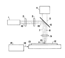
以下、本発明の実施形態を説明する。図1は、本願発明の第1実施形態を実施するナノ周期構造生成用のレーザー照射システムの例である。図1において、超短パルスレーザー発振器1により、超短パルスレーザー光ビームである第2の光ビーム16を放射する。超短パルスとは、100ps以下のパルス幅を有するものとする。超短パルスレーザー発振器1は赤外線波長域の市販のレーザー(たとえば、サイバーレーザー社製モデルIFRIT)を用いることができる。この第2の光ビーム16を偏光方向制御器2で偏光方向を制御し、レーザーパワー減衰器3を通じて、偏光方向とパワーを改質に適する特性の光ビーム18とし、それを表面改質材料12に向けて照射するためのダイクロイックミラー6で反射する。反射された光ビーム8は集光レンズ9で集光されて表面改質材料12の方面に向けて表面改質材料12の表面11に照射される。
Embodiments of the present invention will be described below. FIG. 1 is an example of a laser irradiation system for generating a nano-periodic structure that implements the first embodiment of the present invention. In FIG. 1, an ultrashort pulse laser oscillator 1 emits a
また、第1の光ビーム発生器4から放出された第1の光ビーム5は、ダイクロイックミラー6を通過して集光レンズ9で適度に集光されて表面改質材料の表面11に照射される。第1の光ビーム5は、紫外または可視領域の光とすると好適である。また、連続波(CW)発振、Qスイッチ発振またはモード同期パルス発振から得られるレーザー光とすることができる。またはそれらのレーザー光を非線形光学素子に通して得られる、波長変換光としてもよい。光源の配置として、第1の光ビーム発生器4と第2の光ビーム発生器1の相対位置を交換することができる。この場合、ダイクロイックミラー6の光学特性は2つのビームに対して透過、反射性能が逆になる。
Further, the first light beam 5 emitted from the first light beam generator 4 passes through the
改質面積の処理する大きさがレーザー集光スポット10の面積より大きい場合は、表面改質材料12と重畳2波長ビームとを相対的に移動して改質処理する面積を拡大する。改質材料を移動してその上に重畳2波長ビームを照射する場合は、XYテーブル13に表面改質材料12を搭載してXYテーブル13を駆動部14から発生する駆動信号19に応じて位置、速度等が制御されて走査される。
When the size of the modified area to be processed is larger than the area of the laser focused
このような装置構成により、図2に示すように、周期20のナノ周期構造の凹凸の溝を有するナノ周期構造形成部分15を表面改質材料12の表面11に形成する。周期構造の形成される縞方向は、照射する超短パルスのレーザー光の偏光方向を調整して照射することで設定できる。レーザーパワーは減衰器3により、改質に適するパワーで改質材料の表面11に照射されるように調整して照射する。
With such an apparatus configuration, as shown in FIG. 2, a nano-periodic
表面改質材料12は誘電体の場合は、ガラス材料、有機ポリマー、セラミック、ダイヤモンドまたは窒化ホウ素のほか結晶体、セラミックス、酸化物塗布層などが例として挙げられる。
有機ポリマー材料においては、特にフッ素系ポリマー、たとえば、ポリテトラフルオロエチレン(PTFE)、エチレンテトラフルオロエチレン(ETFE)または熱可塑性フッ素ポリマーが好適であり、製品例としては旭硝子社製サイトップ(登録商標)などがあげられる。
When the
As the organic polymer material, a fluorine-based polymer, for example, polytetrafluoroethylene (PTFE), ethylenetetrafluoroethylene (ETFE) or a thermoplastic fluoropolymer is particularly suitable. As a product example, Cytop (registered trademark) manufactured by Asahi Glass Co., Ltd. is used. ) Etc.
必要に応じて誘電体材料内または表面に金属、半導体または異種の誘電体を添加した複合的な誘電体材料とすることができる。 If necessary, a composite dielectric material in which a metal, a semiconductor, or a different kind of dielectric material is added to or in the surface of the dielectric material can be used.
誘電体表面に第1の光ビームと超短パルスレーザー光である第2の光ビームを同時的に照射する場合、誘電体表面にプラズモンの生成を効果的に行わせるために、誘電体内に金属や半導体イオンをドーピングし、第1の光ビーム照射による支援の他に表面近傍に自由電子を予め分布させ、プラズモンの生成を効率化できる。この場合、第1の光ビームの照射は必ずしも必要とはしない。誘電体内部に添加する方法以外に、材料の雰囲気を化学的誘電体材料に金属を添加する方法として、鍍金法、イオン注入法、化学気相成長、物理気相成長または物理蒸着等の半導体又は金属の表面への添加法などを使用することができる。これらの方法で金属や半導体をレーザービームの照射部範囲内に置く場合、プラズモンの生成源である自由電子が第2の光ビーム照射部に豊富に供給され、レーザー光の強電場の下で高密度のプラズモンの発生が可能で、したがって高密度のレーザー光の偏りのあるエネルギー源が表面近傍に分布し、それにより誘電体材料表面にナノ周期構造が形成される。誘電体材料表面にナノ周期構造が形成された後に、表面近傍に金属や半導体が残留することが望ましくない場合は、周期構造を誘電体表面に残したままエッチングなどにより除去できる。 In the case where the first light beam and the second light beam, which is an ultrashort pulse laser beam, are simultaneously irradiated onto the dielectric surface, in order to effectively generate plasmons on the dielectric surface, In addition to the support by the first light beam irradiation, free electrons can be pre-distributed in the vicinity of the surface to improve the efficiency of plasmon generation. In this case, irradiation with the first light beam is not necessarily required. In addition to the method of adding to the inside of the dielectric, the atmosphere of the material can be added to the chemical dielectric material by using a semiconductor such as a plating method, ion implantation method, chemical vapor deposition, physical vapor deposition or physical vapor deposition, or the like. The addition method to the surface of a metal etc. can be used. When a metal or semiconductor is placed within the area irradiated with the laser beam by these methods, free electrons, which are plasmon generation sources, are abundantly supplied to the second light beam irradiated area, and are high under the strong electric field of the laser beam. Density plasmons can be generated, and therefore a high density laser beam biased energy source is distributed near the surface, thereby forming a nano-periodic structure on the surface of the dielectric material. If it is not desirable that a metal or semiconductor remains in the vicinity of the surface after the nano-periodic structure is formed on the surface of the dielectric material, it can be removed by etching or the like while leaving the periodic structure on the surface of the dielectric.
第1の光ビームは改質材料がアブレーションによって加工されない程度のパワーに設定して、改質材料表面に十分な自由電子が生成可能なようにパワーレベルを設定する。超短パルスレーザー光である第2の光ビームのパワーレベルは熱的な変質が材料に誘起されないエネルギーレベルに上限が調整され、あくまでも干渉現象により、超短パルスとプラズモンの間、超短パルスとその自己散乱光の間で、周期的に光強度が増大される部分で非熱加工が行われ、ナノ周期構造を形成されるものである。第1の光ビームは誘電体表面に第2の光ビームの照射と同時に照射すればよいが、少なくとも第2の光ビームの照射時には自由電子が誘電体表面に滞留、残存していることが望ましい。誘電体内に金属や半導体イオンをドーピングしてあるときは、特に制限しない。 The first light beam is set to such a power that the modified material is not processed by ablation, and the power level is set so that sufficient free electrons can be generated on the surface of the modified material. The upper limit of the power level of the second light beam, which is an ultra-short pulse laser beam, is adjusted to the energy level at which no thermal alteration is induced in the material. Non-thermal processing is performed at a portion where the light intensity is periodically increased among the self-scattered light, and a nano-periodic structure is formed. The first light beam may be irradiated onto the dielectric surface simultaneously with the irradiation of the second light beam, but it is desirable that free electrons stay and remain on the dielectric surface at least during the irradiation of the second light beam. . There is no particular limitation when the dielectric is doped with metal or semiconductor ions.
第1の光ビーム照射で生成した自由電子は放置する場合、緩和消滅までの短時間だけ寿命を持って存続するので、その存続期間に第2の光ビームを照射すれば、必ずしも第1の光ビームと第2の光ビームとの照射開始時間が同時でなくても2波長の照射の効果は得ることができる。第1の光ビームと第2の光ビームとの照射は空間的に重なり合った部分で改質が十分行うことができる。照射パルスのスポットサイズより大面積を改質する場合は、改質対象の材料の表面を2波長の照射場所を走査して大面積を処理することができる。 When the free electrons generated by the first light beam irradiation are left unattended, they last for a short time until the relaxation disappears. Therefore, if the second light beam is irradiated during the lifetime, the first light is not necessarily generated. Even if the irradiation start times of the beam and the second light beam are not simultaneous, the effect of irradiation with two wavelengths can be obtained. Irradiation with the first light beam and the second light beam can be sufficiently modified in a spatially overlapping portion. In the case of modifying a larger area than the spot size of the irradiation pulse, the surface of the material to be modified can be scanned at the two-wavelength irradiation place to process the large area.
改質材料に照射するレーザービームの入射角度は、垂直入射に限定されない、ナノ周期構造の周期20は1nm〜1μmの範囲で入射角度、発振波長、パワーレベル等を変化し、用途に適した改質構造を得ることができる。装飾品として、ナノ周期構造を表面の光学的性質改変に用いる場合は、ナノ周期構造が周期が200nmより大きければ、反射光が回折効果によって分光されるので、その作用を有効に適用して装飾品の美的価値の向上に利用できる。さらに、このナノ周期構造を各種材料に適用すれば、周期構造の溝の方向に直交する面内での観察者に対してだけ読み取りが可能になる視認方向を制限する効果も得られる。
The incident angle of the laser beam irradiating the modifying material is not limited to normal incidence, and the
つぎに第2の実施形態を説明する。第1の実施形態では、第1の光ビームと第2の光ビームを別個に供給したが、この実施形態では同一のレーザー光源を用いる。すなわち、第2の光ビームを超短パルスレーザーとし、それを短波長化した成分を第2光ビームとする。短波長化には、高調波を発生する既存の非線形光学結晶を用いることができる。例えば、該超短パルスレーザーの波長を780nm〜1100nmとすると、この基本波を第2の光ビームとし、その第2高調波の390nm〜550nmまたは第3高調波の260nm〜370nmの超短パルスを第1の光ビームに用いることができる。これらの波長は可視領域または紫外領域に属する。 Next, a second embodiment will be described. In the first embodiment, the first light beam and the second light beam are separately supplied. In this embodiment, the same laser light source is used. That is, the second light beam is an ultrashort pulse laser, and the component of which the wavelength is shortened is the second light beam. For shortening the wavelength, an existing nonlinear optical crystal that generates harmonics can be used. For example, if the wavelength of the ultrashort pulse laser is 780 nm to 1100 nm, this fundamental wave is used as the second light beam, and the second harmonic 390 nm to 550 nm or the third harmonic 260 nm to 370 nm is used. It can be used for the first light beam. These wavelengths belong to the visible region or the ultraviolet region.
該第2高調波である波長390nm〜550nmの領域を第1の光ビームとして用いると、ガラスなどのワイドギャップ材料の被加工物質に対して好適である。この波長領域はガラスなどのワイドバンドギャップ材料に容易に多光子吸収で固体内にプラズマを生成するので、同時もしくは後続する第2の光ビームである基本波のパルスが作用してナノ周期構造が形成されるためである。 The use of a region having a wavelength of 390 nm to 550 nm, which is the second harmonic, as the first light beam is suitable for a material to be processed of a wide gap material such as glass. Since this wavelength region easily generates a plasma in a solid by multiphoton absorption in a wide band gap material such as glass, a nano-periodic structure is formed by the action of a pulse of the fundamental wave which is the second light beam simultaneously or subsequently. This is because it is formed.
図3は、本願発明の第2実施形態を実施するナノ周期構造生成用のレーザー照射システムの例である。超短パルスを発生するレーザー発振部21における媒体は、波長780〜820nmのチタンサファイア結晶、若しくは1030〜1100nmのイッテルビウム(Yb)をドープした結晶(YAG,KYW)、またはYbをドープしたガラスファイバーが好適である。
FIG. 3 is an example of a laser irradiation system for generating a nano-periodic structure that implements the second embodiment of the present invention. The medium in the
レーザー発振部21からの出力ビーム22を波長板(例えば、2分の1波長板)23を用いて偏光面の方向を回転する。さらに、非線形光学結晶からなる波長変換部25において、基本波の波長の2分の1、3分の1、又は4分の1の紫外または可視領域のレーザー光である第1のレーザー光を発生させる。この変換技術は周知の波長変換技術を用いることができるからここでは詳細は省略する。非線形光学結晶の結晶軸方向と変換前のレーザー光の直線偏光面の相対的な関係は高調波発生の変換効率に影響するので、波長板23は変換効率の調整のために設置してある。出力ビーム22は波長変換部25内を通過すると、波長変換されないで通過した基本波成分の第2のレーザー光28と変換された第1のレーザー光29とになる。両者の割合は変換効率によって決められ、適度な比率で混合した2波長レーザー光26が同軸配置で得られる。
The direction of the plane of polarization of the
この2波長レーザー光26は波長分割フィルタ27によって、第1のレーザー光29と第2のレーザー光28の成分に分岐される。第1のレーザー光29は波長分割フィルタ27によって反射されて波長合成フィルタ37に向けられる。一方、第2のレーザー光28は波長分割フィルタ27を通過して全反射ミラー31、32を有する光路迂回ユニット39を経由し、波長合成フィルタ37に向けられる。光路迂回ユニット39により、第2のレーザー光28は、第1のレーザー光29よりも長い光路を走行するので、光路差走行時間に応じた遅延時間が付与される。光路差を変化することにより、第1のレーザー光照射から第2のレーザー光照射までの遅延時間を変化することができる。第1のレーザー光29と第2のレーザー光28とは波長合成フィルタ37によって合成され、照射用レーザー光38として同軸上に再度配置される。
The two-
波長変換部25の出力の時点では2波長レーザー光26の第1のレーザー光29と第2のレーザー光28とは時間的に十分重畳していた。光路差を与えることにより、照射用レーザー光38においては、第1のレーザー光29のパルスが先に全反射ミラー35に主パルス部分が到達し、第2のレーザー光28のパルスは遅延時間遅れて全反射ミラー35に到達する。第1の光ビーム照射で生成した自由電子は放置すると緩和消滅までの短時間だけ寿命を持って存続するので、その存続期間の内に第2の光ビームを照射するような、遅延時間を付与すればよい。また、光路迂回ユニット39を除去し、波長分割フィルタ27及び波長合成フィルタ37を全反射ミラーに代えるなどして、光路差を付与しない構成にすると第1の光ビームと第2の光ビームとを同時に照射することができる。
At the time of output of the
2波長のレーザー光は空間的に重なって集光レンズ9に入射する。集光レンズ9に入射した以後は、表面改質材料12の方面に向けて表面改質材料12の表面11に照射される。改質面積の処理する大きさがレーザー集光スポット10の面積より大きい場合は、表面改質材料12と2波長レーザー光26とを相対的に移動して改質処理する面積を拡大する。改質材料を移動してその上に2波長レーザー光を照射する場合は、XYテーブル13に表面改質材料12を搭載してXYテーブル13を駆動部14から発生する駆動信号19に応じて位置、速度等が制御されて走査される。
The two-wavelength laser light is spatially overlapped and enters the condenser lens 9. After entering the condenser lens 9, the surface 11 of the
このような装置構成により、第1の実施形態と同様、図2に示される、周期20のナノ周期構造の凹凸の溝を有するナノ周期構造形成部分15が表面改質材料12の表面11に形成される。表面改質材料12である誘電体材料の例、被加工物体に金属、半導体または異種の誘電体を添加することができる点、誘電体内に金属や半導体イオンをドーピングすると、第1の光ビーム照射による支援の他に表面近傍に自由電子を予め分布させ、プラズモンの生成を効率化できる点、第1及び第2光ビームのパワーの設定、及びレーザービームの照射角度など、第1の実施形態に対する記載は本実施形態にも適用される。
By such an apparatus configuration, as in the first embodiment, the nano-periodic
本発明のナノ周期構造形成方法によれば、表面改質を施す誘電体の材料表面に第1の光ビームを照射すると同時的に超短パルスの高ピークパワーを備えた第2の光ビームを該材料表面に照射することにより、表面に周期構造のピッチが1nm〜1μmの改質層を形成することが可能である。第1の光ビームを材料表面に照射することで材料表面に自由電子層を形成することでプラズモンの形成を支援し、同時的に照射する超短パルスの高パワー密度の第2の光ビームによって表面にプラズモンを形成し、そこに高エネルギー電場を形成し、その作用で材料表面に超微細な凹凸の周期構造を形成する。 According to the method of forming a nano-periodic structure of the present invention, when a first light beam is irradiated on the surface of a dielectric material to be surface-modified, a second light beam having a high peak power of an ultrashort pulse is simultaneously generated. By irradiating the surface of the material, it is possible to form a modified layer having a periodic structure pitch of 1 nm to 1 μm on the surface. By irradiating the surface of the material with the first light beam, a free electron layer is formed on the surface of the material to assist in the formation of plasmons. A plasmon is formed on the surface, a high energy electric field is formed there, and an ultrafine irregular periodic structure is formed on the material surface by the action.
本発明のナノ周期構造形成方法によって周期構造を材料表面に形成することにより、ガラス材料、建築材料、モバイル装置の表示部や装飾部に撥水性、光沢の付与、などの機能を与え、水滴による曇り防止、光学的な反射光干渉作用による着色性、回折による視認性増加などの有用な効果が得られる。 By forming the periodic structure on the surface of the material by the nano-periodic structure forming method of the present invention, functions such as water repellency and glossiness are imparted to the display part and decoration part of the glass material, building material, and mobile device. Useful effects such as anti-fogging, colorability due to optical reflected light interference, and increased visibility due to diffraction can be obtained.
さらに本発明のナノ周期構造形成方法によって表面改質を施したダイヤモンド、窒素化ホウ素などの刃を有する切削工具では、摩擦低減などにより切削速度向上に寄与できる。また、本発明のナノ周期構造形成方法によって表面改質を施した装飾用ダイヤモンド等の結晶材料では、表面の反射機能の変化を起こすことで新たな製品価値の創生がなされる。 Further, a cutting tool having a blade such as diamond or boron nitride subjected to surface modification by the nano-periodic structure forming method of the present invention can contribute to an improvement in cutting speed by reducing friction. In addition, in a crystal material such as a decorative diamond subjected to surface modification by the nano-periodic structure forming method of the present invention, a new product value is created by causing a change in the reflective function of the surface.
本発明の活用例として、液晶表示装置のガラスの表面処理、工具類の表面処理で長寿命化や切削性能向上、装飾用結晶類のマーキング、光学的な輝きを増加する表面処理の実施、各種表面性状の改質で撥水性を付与すること、ガラスの曇り防止などに適用できる。 Examples of utilization of the present invention include surface treatment of glass for liquid crystal display devices, longer life and improved cutting performance by surface treatment of tools, marking of decorative crystals, implementation of surface treatment to increase optical brightness, various It can be applied to impart water repellency by modifying the surface properties and to prevent fogging of glass.
1:超短パルスレーザー発振器
2:偏光方向制御器
3:レーザーパワー減衰器
4:第1の光ビーム発生器
5:第1の光ビーム
6:ダイクロイックミラー
8:第2の光ビーム
9:集光レンズ
10:レーザー集光スポット
11:表面改質材料の表面
12:表面改質材料
13:XYテーブル
14:XYテーブル駆動部
15:ナノ周期構造形成部分
16、18:第2の光ビーム
19:駆動信号
20:ナノ周期構造の周期
21:レーザー発振部
22:レーザー発振部からの出力ビーム
23:波長板
25:波長変換部
26:2波長レーザー光
27:波長分割フィルタ
28:第2のレーザー光
29:第1のレーザー光
31、32:全反射ミラー
35:全反射ミラー
37:波長合成フィルタ
38:照射用レーザー光
39:光路迂回ユニット
1: Ultrashort pulse laser oscillator 2: Polarization direction controller 3: Laser power attenuator 4: First light beam generator 5: First light beam 6: Dichroic mirror 8: Second light beam 9: Condensing Lens 10: Laser focusing spot 11: Surface of surface modifying material 12: Surface modifying material 13: XY table 14: XY table driving unit 15: Nano periodic
Claims (13)
Priority Applications (1)
| Application Number | Priority Date | Filing Date | Title |
|---|---|---|---|
| JP2008325424A JP2010142862A (en) | 2008-12-22 | 2008-12-22 | Method for producing nano-periodic structure on surface of dielectric material |
Applications Claiming Priority (1)
| Application Number | Priority Date | Filing Date | Title |
|---|---|---|---|
| JP2008325424A JP2010142862A (en) | 2008-12-22 | 2008-12-22 | Method for producing nano-periodic structure on surface of dielectric material |
Publications (1)
| Publication Number | Publication Date |
|---|---|
| JP2010142862A true JP2010142862A (en) | 2010-07-01 |
Family
ID=42563833
Family Applications (1)
| Application Number | Title | Priority Date | Filing Date |
|---|---|---|---|
| JP2008325424A Pending JP2010142862A (en) | 2008-12-22 | 2008-12-22 | Method for producing nano-periodic structure on surface of dielectric material |
Country Status (1)
| Country | Link |
|---|---|
| JP (1) | JP2010142862A (en) |
Cited By (19)
| Publication number | Priority date | Publication date | Assignee | Title |
|---|---|---|---|---|
| JP2011152578A (en) * | 2010-01-28 | 2011-08-11 | Utsunomiya Univ | Laser beam machining device |
| JP2012240082A (en) * | 2011-05-19 | 2012-12-10 | Disco Corp | Laser processing method and laser processing apparatus |
| JP2013539911A (en) * | 2010-09-21 | 2013-10-28 | 中国科学院理化技術研究所 | Laser micro / nano processing system and method |
| WO2014017655A1 (en) * | 2012-07-26 | 2014-01-30 | デクセリアルズ株式会社 | Microfabrication method |
| DE102012025294A1 (en) * | 2012-12-28 | 2014-07-03 | Laser Zentrum Hannover E.V. | Method for producing structures on a surface of a workpiece |
| JP2015013786A (en) * | 2012-07-26 | 2015-01-22 | デクセリアルズ株式会社 | Microfabrication method |
| JP2015024938A (en) * | 2013-07-26 | 2015-02-05 | デクセリアルズ株式会社 | Fine processing method |
| CN104487394A (en) * | 2012-07-26 | 2015-04-01 | 迪睿合电子材料有限公司 | Microfabrication method |
| JP2015533654A (en) * | 2012-09-24 | 2015-11-26 | エレクトロ サイエンティフィック インダストリーズ インコーポレーテッド | Method and apparatus for machining a workpiece |
| WO2015189645A1 (en) * | 2014-06-13 | 2015-12-17 | The Science And Technology Facilities Council | Apparatus and methods relating to reduced photoelectron yield and/or secondary electron yield |
| CN105655865A (en) * | 2016-01-13 | 2016-06-08 | 山西大学 | Method and device for utilizing pulse lasers to irradiate single-layer molybdenum disulfide to realize optical modification |
| US9828278B2 (en) | 2012-02-28 | 2017-11-28 | Electro Scientific Industries, Inc. | Method and apparatus for separation of strengthened glass and articles produced thereby |
| JP2018149574A (en) * | 2017-03-13 | 2018-09-27 | 株式会社ディスコ | Laser processing device |
| JP2018149571A (en) * | 2017-03-13 | 2018-09-27 | 株式会社ディスコ | Laser processing method and laser processing device |
| JP2018149573A (en) * | 2017-03-13 | 2018-09-27 | 株式会社ディスコ | Laser processing device |
| JP2018149572A (en) * | 2017-03-13 | 2018-09-27 | 株式会社ディスコ | Laser processing device |
| JP2019042812A (en) * | 2018-10-30 | 2019-03-22 | デクセリアルズ株式会社 | Microstructure and manufacturing method of the same, and composition for manufacturing microstructure |
| CN110171801A (en) * | 2019-05-15 | 2019-08-27 | 浙江大学 | The preparation method of glass and the alternately arranged self-organizing periodicity micro-nano structure of crystal |
| CN112355483A (en) * | 2020-10-30 | 2021-02-12 | 北京理工大学 | Method for preparing submicron concentric rings on silicon surface by femtosecond laser |
Citations (8)
| Publication number | Priority date | Publication date | Assignee | Title |
|---|---|---|---|---|
| JPH08195437A (en) * | 1993-10-15 | 1996-07-30 | Texas Instr Inc <Ti> | Flattening structure for reducing line capacity |
| JP2002289604A (en) * | 2001-03-27 | 2002-10-04 | Japan Science & Technology Corp | Circuit board and its manufacturing method |
| JP2002289618A (en) * | 2001-03-28 | 2002-10-04 | Mitsubishi Heavy Ind Ltd | Method and apparatus for forming film |
| JP2002299519A (en) * | 2001-03-30 | 2002-10-11 | Kyocera Corp | Composite ceramic substrate |
| JP2003318258A (en) * | 2002-04-17 | 2003-11-07 | Samsung Electronics Co Ltd | Forming method of dual damascene wiring using low permeability insulating film |
| JP2006212646A (en) * | 2005-02-01 | 2006-08-17 | Canon Machinery Inc | Method for preparing periodic structure |
| JP2008004615A (en) * | 2006-06-20 | 2008-01-10 | Ebara Corp | Method and apparatus for forming wiring |
| JP2008272794A (en) * | 2007-04-27 | 2008-11-13 | Cyber Laser Kk | Laser beam machining method and apparatus |
-
2008
- 2008-12-22 JP JP2008325424A patent/JP2010142862A/en active Pending
Patent Citations (8)
| Publication number | Priority date | Publication date | Assignee | Title |
|---|---|---|---|---|
| JPH08195437A (en) * | 1993-10-15 | 1996-07-30 | Texas Instr Inc <Ti> | Flattening structure for reducing line capacity |
| JP2002289604A (en) * | 2001-03-27 | 2002-10-04 | Japan Science & Technology Corp | Circuit board and its manufacturing method |
| JP2002289618A (en) * | 2001-03-28 | 2002-10-04 | Mitsubishi Heavy Ind Ltd | Method and apparatus for forming film |
| JP2002299519A (en) * | 2001-03-30 | 2002-10-11 | Kyocera Corp | Composite ceramic substrate |
| JP2003318258A (en) * | 2002-04-17 | 2003-11-07 | Samsung Electronics Co Ltd | Forming method of dual damascene wiring using low permeability insulating film |
| JP2006212646A (en) * | 2005-02-01 | 2006-08-17 | Canon Machinery Inc | Method for preparing periodic structure |
| JP2008004615A (en) * | 2006-06-20 | 2008-01-10 | Ebara Corp | Method and apparatus for forming wiring |
| JP2008272794A (en) * | 2007-04-27 | 2008-11-13 | Cyber Laser Kk | Laser beam machining method and apparatus |
Cited By (27)
| Publication number | Priority date | Publication date | Assignee | Title |
|---|---|---|---|---|
| JP2011152578A (en) * | 2010-01-28 | 2011-08-11 | Utsunomiya Univ | Laser beam machining device |
| JP2013539911A (en) * | 2010-09-21 | 2013-10-28 | 中国科学院理化技術研究所 | Laser micro / nano processing system and method |
| JP2012240082A (en) * | 2011-05-19 | 2012-12-10 | Disco Corp | Laser processing method and laser processing apparatus |
| US9193008B2 (en) | 2011-05-19 | 2015-11-24 | Disco Corporation | Laser processing method and laser processing apparatus |
| US9828278B2 (en) | 2012-02-28 | 2017-11-28 | Electro Scientific Industries, Inc. | Method and apparatus for separation of strengthened glass and articles produced thereby |
| WO2014017655A1 (en) * | 2012-07-26 | 2014-01-30 | デクセリアルズ株式会社 | Microfabrication method |
| JP2015013786A (en) * | 2012-07-26 | 2015-01-22 | デクセリアルズ株式会社 | Microfabrication method |
| CN104487394A (en) * | 2012-07-26 | 2015-04-01 | 迪睿合电子材料有限公司 | Microfabrication method |
| US11242284B2 (en) | 2012-07-26 | 2022-02-08 | Dexerials Corporation | Microfabrication method |
| JP2015533654A (en) * | 2012-09-24 | 2015-11-26 | エレクトロ サイエンティフィック インダストリーズ インコーポレーテッド | Method and apparatus for machining a workpiece |
| US10357850B2 (en) | 2012-09-24 | 2019-07-23 | Electro Scientific Industries, Inc. | Method and apparatus for machining a workpiece |
| EP2897760A4 (en) * | 2012-09-24 | 2016-07-20 | Electro Scient Ind Inc | Method and apparatus for machining a workpiece |
| TWI611856B (en) * | 2012-09-24 | 2018-01-21 | 伊雷克托科學工業股份有限公司 | Method of laser machining, laser-machined article and laser-machining apparatus |
| DE102012025294A1 (en) * | 2012-12-28 | 2014-07-03 | Laser Zentrum Hannover E.V. | Method for producing structures on a surface of a workpiece |
| JP2015024938A (en) * | 2013-07-26 | 2015-02-05 | デクセリアルズ株式会社 | Fine processing method |
| WO2015189645A1 (en) * | 2014-06-13 | 2015-12-17 | The Science And Technology Facilities Council | Apparatus and methods relating to reduced photoelectron yield and/or secondary electron yield |
| CN105655865B (en) * | 2016-01-13 | 2018-10-16 | 山西大学 | Pulsed laser irradiation single layer molybdenum disulfide realizes the method and device of optical modifier |
| CN105655865A (en) * | 2016-01-13 | 2016-06-08 | 山西大学 | Method and device for utilizing pulse lasers to irradiate single-layer molybdenum disulfide to realize optical modification |
| JP2018149574A (en) * | 2017-03-13 | 2018-09-27 | 株式会社ディスコ | Laser processing device |
| JP2018149571A (en) * | 2017-03-13 | 2018-09-27 | 株式会社ディスコ | Laser processing method and laser processing device |
| JP2018149573A (en) * | 2017-03-13 | 2018-09-27 | 株式会社ディスコ | Laser processing device |
| JP2018149572A (en) * | 2017-03-13 | 2018-09-27 | 株式会社ディスコ | Laser processing device |
| JP2019042812A (en) * | 2018-10-30 | 2019-03-22 | デクセリアルズ株式会社 | Microstructure and manufacturing method of the same, and composition for manufacturing microstructure |
| CN110171801A (en) * | 2019-05-15 | 2019-08-27 | 浙江大学 | The preparation method of glass and the alternately arranged self-organizing periodicity micro-nano structure of crystal |
| CN110171801B (en) * | 2019-05-15 | 2022-01-07 | 浙江大学 | Preparation method of self-organized periodic micro-nano structure with alternately arranged glass and crystals |
| CN112355483A (en) * | 2020-10-30 | 2021-02-12 | 北京理工大学 | Method for preparing submicron concentric rings on silicon surface by femtosecond laser |
| CN112355483B (en) * | 2020-10-30 | 2021-08-24 | 北京理工大学 | Method for preparing submicron concentric rings on silicon surface by femtosecond laser |
Similar Documents
| Publication | Publication Date | Title |
|---|---|---|
| JP2010142862A (en) | Method for producing nano-periodic structure on surface of dielectric material | |
| Lei et al. | Ultrafast laser applications in manufacturing processes: A state-of-the-art review | |
| Tsukamoto et al. | Periodic microstructures produced by femtosecond laser irradiation on titanium plate | |
| TW201026420A (en) | Method and apparatus for forming grooves in the surface of a polymer layer | |
| US11482826B2 (en) | Optical processing apparatus, optical processing method, and optically-processed product production method | |
| CN104625416B (en) | Based on square hole auxiliary electron dynamic regulation crystal silicon surface periodic micro-nano structure method | |
| CA2604641A1 (en) | Method for finely polishing/structuring thermosensitive dielectric materials by a laser beam | |
| JP2005132694A (en) | Glass cutting method | |
| JP2008126283A (en) | Manufacturing method of microstructure and exposure method | |
| JP2011091322A (en) | Laser dicing method and laser dicing device | |
| Liu et al. | Optical quality laser polishing of CVD diamond by UV pulsed laser irradiation | |
| He et al. | Controlling periodic ripple microstructure formation on 4H-SiC crystal with three time-delayed femtosecond laser beams of different linear polarizations | |
| KR100636852B1 (en) | Scribing method and cutting method for glass using mode-locked uv-laser | |
| KR100723935B1 (en) | Laser pattern device | |
| Deladurantaye et al. | Material micromachining using a pulsed fiber laser platform with fine temporal nanosecond pulse shaping capability | |
| JP2008049380A (en) | Method for forming microstructure of surface by laser beam | |
| JP2007012733A (en) | Dividing method of substrate | |
| JP2006247665A (en) | Method and apparatus for laser beam machining | |
| Butkus et al. | Micromachining of transparent, semiconducting and metallic substrates using femtosecond laser beams | |
| Wu et al. | Nano-periodic structure formation on titanium thin film with a Femtosecond laser | |
| Lan et al. | Laser precision engineering of glass substrates | |
| KR101243269B1 (en) | Laser processing system and laser processing method using the same | |
| WO2018010707A1 (en) | Method and system of ultrafast laser writing of highly-regular periodic structures | |
| CN116511719B (en) | Method and system for preparing micro-nano structure by laser-electron beam and micro-nano structure | |
| Yuan et al. | Periodic nanohole array structure induced on a silicon surface by direct writing with a femtosecond laser |
Legal Events
| Date | Code | Title | Description |
|---|---|---|---|
| A621 | Written request for application examination |
Free format text: JAPANESE INTERMEDIATE CODE: A621 Effective date: 20111222 |
|
| A977 | Report on retrieval |
Free format text: JAPANESE INTERMEDIATE CODE: A971007 Effective date: 20130322 |
|
| A131 | Notification of reasons for refusal |
Free format text: JAPANESE INTERMEDIATE CODE: A131 Effective date: 20130326 |
|
| A521 | Written amendment |
Free format text: JAPANESE INTERMEDIATE CODE: A523 Effective date: 20130520 |
|
| A02 | Decision of refusal |
Free format text: JAPANESE INTERMEDIATE CODE: A02 Effective date: 20130716 |