JP2010114106A - Transfer method of functional region, led array, led printer head, and led printer - Google Patents
Transfer method of functional region, led array, led printer head, and led printer Download PDFInfo
- Publication number
- JP2010114106A JP2010114106A JP2008282681A JP2008282681A JP2010114106A JP 2010114106 A JP2010114106 A JP 2010114106A JP 2008282681 A JP2008282681 A JP 2008282681A JP 2008282681 A JP2008282681 A JP 2008282681A JP 2010114106 A JP2010114106 A JP 2010114106A
- Authority
- JP
- Japan
- Prior art keywords
- substrate
- layer
- region
- functional region
- functional
- Prior art date
- Legal status (The legal status is an assumption and is not a legal conclusion. Google has not performed a legal analysis and makes no representation as to the accuracy of the status listed.)
- Pending
Links
Images


Classifications
-
- H—ELECTRICITY
- H01—ELECTRIC ELEMENTS
- H01L—SEMICONDUCTOR DEVICES NOT COVERED BY CLASS H10
- H01L27/00—Devices consisting of a plurality of semiconductor or other solid-state components formed in or on a common substrate
- H01L27/15—Devices consisting of a plurality of semiconductor or other solid-state components formed in or on a common substrate including semiconductor components with at least one potential-jump barrier or surface barrier specially adapted for light emission
- H01L27/153—Devices consisting of a plurality of semiconductor or other solid-state components formed in or on a common substrate including semiconductor components with at least one potential-jump barrier or surface barrier specially adapted for light emission in a repetitive configuration, e.g. LED bars
-
- B—PERFORMING OPERATIONS; TRANSPORTING
- B41—PRINTING; LINING MACHINES; TYPEWRITERS; STAMPS
- B41J—TYPEWRITERS; SELECTIVE PRINTING MECHANISMS, i.e. MECHANISMS PRINTING OTHERWISE THAN FROM A FORME; CORRECTION OF TYPOGRAPHICAL ERRORS
- B41J2/00—Typewriters or selective printing mechanisms characterised by the printing or marking process for which they are designed
- B41J2/435—Typewriters or selective printing mechanisms characterised by the printing or marking process for which they are designed characterised by selective application of radiation to a printing material or impression-transfer material
- B41J2/447—Typewriters or selective printing mechanisms characterised by the printing or marking process for which they are designed characterised by selective application of radiation to a printing material or impression-transfer material using arrays of radiation sources
- B41J2/45—Typewriters or selective printing mechanisms characterised by the printing or marking process for which they are designed characterised by selective application of radiation to a printing material or impression-transfer material using arrays of radiation sources using light-emitting diode [LED] or laser arrays
-
- H—ELECTRICITY
- H01—ELECTRIC ELEMENTS
- H01L—SEMICONDUCTOR DEVICES NOT COVERED BY CLASS H10
- H01L33/00—Semiconductor devices with at least one potential-jump barrier or surface barrier specially adapted for light emission; Processes or apparatus specially adapted for the manufacture or treatment thereof or of parts thereof; Details thereof
- H01L33/005—Processes
- H01L33/0093—Wafer bonding; Removal of the growth substrate
Abstract
Description
本発明は、半導体部材、半導体物品、半導体素子などを製造するための機能性領域を移設する方法に関する。また、本発明は、該方法を用いて作製されるLEDアレイ、LEDプリンタヘッド、LEDプリンタ等に関する。 The present invention relates to a method for transferring a functional region for manufacturing a semiconductor member, a semiconductor article, a semiconductor element, or the like. The present invention also relates to an LED array, an LED printer head, an LED printer, and the like manufactured using the method.
GaAs基板上に犠牲層を介して成膜された発光ダイオード構成層を、シリコン基板上に移設(転写ともいう)する技術が知られている。 A technique is known in which a light emitting diode constituent layer formed on a GaAs substrate via a sacrificial layer is transferred (also referred to as transfer) onto a silicon substrate.
特許文献1には、シリコン基板上に、発光ダイオード構成層を移設する技術が記載されている。具体的には、まず、GaAs基板上に犠牲層を介して形成した発光ダイオード構成層に対して、それを発光領域毎に分割するための溝を設ける。該溝の直下には、前記犠牲層が露出している。次に、ドライフィルムレジストを前記発光ダイオード構成層に貼り付け、更に、このドライフィルムレジストにメタルワイヤからなるメッシュ状の支持部材を貼り合わせる。 Patent Document 1 describes a technique for transferring a light emitting diode constituent layer on a silicon substrate. Specifically, first, a groove for dividing the light-emitting diode constituting layer formed on the GaAs substrate via the sacrificial layer for each light-emitting region is provided. The sacrificial layer is exposed immediately below the groove. Next, a dry film resist is affixed to the said light emitting diode structural layer, and also the mesh-shaped support member which consists of metal wires is affixed on this dry film resist.
その後、前記レジストの内、前記メタルワイヤの直下に位置する部分以外を除去する。そして、メッシュ状の支持部材を介して、エッチング液と前記犠牲層とを接触させて、該犠牲層のエッチングを行うことで、GaAs基板を前記貼り合わせ構造体から分離する。更に、GaAs基板を分離した後に、今度はシリコン基板と前記発光ダイオード構成層とを貼り合わせる。こうして、シリコン基板上に発光ダイオード構成層が移設(転写)される。 Thereafter, portions of the resist other than those located immediately below the metal wires are removed. Then, the etching solution and the sacrificial layer are brought into contact with each other through the mesh-shaped support member, and the sacrificial layer is etched, whereby the GaAs substrate is separated from the bonded structure. Further, after separating the GaAs substrate, the silicon substrate and the light emitting diode constituting layer are bonded together. Thus, the light emitting diode constituent layer is transferred (transferred) onto the silicon substrate.
また、特許文献2には、基板上に設けられた複数の半導体チップから選択された一部のチップを他の基板に実装する技術が開示されている。具体的には、第1基板の上に素子を含むデバイス層を有する第1積層体を準備し、第2基板の上に分離層を有する第2積層体を準備する。次いで、前記デバイス層と前記分離層とが対向する様に、前記第1積層体と前記第2積層体とを接合する。更に、前記デバイス層及び前記分離層を含む積層体を所定のパターンで分離して、前記第2基板の上に、前記素子を含む複数のチップを形成する。そして、前記チップから選択した所定のチップと第3基板とを該第3基板の所定位置で接合し、その後、前記分離層において前記第2基板と該所定のチップとを分離し、該所定のチップを前記第3基板に実装する。
GaAs基板上のGaAs等の化合物半導体を発光層に用いてLEDアレイ等を作成する場合、該GaAs基板はシリコン基板と比較して非常に高価であり、GaAs基板の有効利用が求められている。また、GaAs基板の大きさ(例えば2、4、6インチ基板)とシリコン基板(例えば4、5、6、8、12インチ基板)との大きさとが異なる場合、基板単位で一括して移設すると移設可能な領域は小さい方の基板の領域となる。従って、効率良く移設するためには両方の基板を小さい方の基板の大きさに合わせる必要があるという制約がある。 When an LED array or the like is formed using a compound semiconductor such as GaAs on a GaAs substrate as a light emitting layer, the GaAs substrate is very expensive as compared with a silicon substrate, and effective use of the GaAs substrate is required. If the size of the GaAs substrate (for example, 2, 4, 6 inch substrate) and the size of the silicon substrate (for example, 4, 5, 6, 8, 12 inch substrate) are different, The transferable area is the area of the smaller substrate. Therefore, in order to transfer efficiently, there is a restriction that both substrates need to be matched to the size of the smaller substrate.
特許文献1に開示されている様な移設を行うと、有効に活用できるGaAs半導体層は、移設先のシリコン基板上に形成された素子に対応する部分のみであって、素子の存在しない素子間の部分のGaAs半導体は活用されることなく廃棄される。 When the transfer as disclosed in Patent Document 1 is performed, the GaAs semiconductor layer that can be effectively used is only a portion corresponding to the element formed on the transfer destination silicon substrate, and between the elements where no element exists. This portion of the GaAs semiconductor is discarded without being utilized.
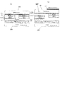
この課題について図面を用いて更に説明する。
図19(a)、(b)は、夫々、シリコン基板上に形成された回路素子及びGaAs基板に形成された発光層を示す図である。図19において、11はGaAs基板、12はGaAsからなる発光層、13はシリコン基板、14はシリコン基板上に形成された回路素子を示す。発光層12を回路素子14上に移設することで発光素子が完成する。この発光層12は回路素子14上の一部(或いは回路素子に隣接して)設けられ、その大きさは10mm×50μm程度の大きさである。一方、回路素子14の大きさは例えば10mm×0.3mm程度の大きさである。従って、一括して発光層12を回路素子14に移設する場合の発光層12の配列及び取り個数は、回路素子14の配列に制約され、結果としてGaAs基板11の単位面積当たりで発光層12として活用できる面積は小さなものとなる。
This problem will be further described with reference to the drawings.
FIGS. 19A and 19B are diagrams showing a circuit element formed on a silicon substrate and a light emitting layer formed on a GaAs substrate, respectively. In FIG. 19, 11 is a GaAs substrate, 12 is a light emitting layer made of GaAs, 13 is a silicon substrate, and 14 is a circuit element formed on the silicon substrate. The light emitting element is completed by transferring the
一方、特許文献2には、1つの基板に多くのチップを形成しておき、これらのチップからチップの一部を選択的に実装する技術が開示されている。従って、この技術によれば、実装元(移設元)の基板上に複数の実装先(移設先)分のチップを形成することができるので、或る程度の基板の有効活用ができる。しかし、特許文献2の技術によれば、チップを選択的に実装する際に、実装するチップに接着剤を塗布しているが、次の様なことが起きる可能性がある。すなわち、チップサイズが小さくなる(例えば、縦、横いずれか一方の幅が数百μm以下)と、この様な方法では、接着剤が実装対象となるチップからはみ出す場合がある。接着剤がはみ出した場合、実装する予定の本来ないチップまで接着され、実装に不具合が生じ、結果として歩留まりが低下する可能性がある。そのため、更に基板を有効活用するための工夫が求められる。 On the other hand, Patent Document 2 discloses a technology in which many chips are formed on one substrate and a part of the chips is selectively mounted from these chips. Therefore, according to this technique, chips for a plurality of mounting destinations (transfer destinations) can be formed on a substrate of a mounting source (transfer source), so that a certain amount of board can be effectively used. However, according to the technique of Patent Document 2, when a chip is selectively mounted, an adhesive is applied to the chip to be mounted, but the following may occur. That is, when the chip size is small (for example, either the vertical or horizontal width is several hundred μm or less), in such a method, the adhesive may protrude from the chip to be mounted. When the adhesive protrudes, even a chip that is not originally intended to be mounted is bonded, which may cause a problem in mounting, resulting in a decrease in yield. Therefore, a device for effectively utilizing the substrate is required.
また、チップサイズが小さくなると、接着剤の厚さも、チップからはみ出さない様にするには薄くせざるを得ない。この様な状態で接着すると、接着時に実装予定のないチップが実装用の基板と接触することで破損する可能性がある。 Further, when the chip size is reduced, the thickness of the adhesive must be reduced so as not to protrude from the chip. If bonding is performed in such a state, there is a possibility that a chip that is not to be mounted at the time of bonding will be damaged by coming into contact with the mounting substrate.
上記課題に鑑み、分離層を有する第1の基板の前記分離層の上に接合されて設けられている2以上の機能性領域の中の一部の領域を他の基板に移設する本発明の機能性領域の移設方法は次の工程を含むことを特徴とする。
前記機能性領域に含まれる第1の機能性領域と、前記他の基板である第2の基板上の前記第1の機能性領域が移設される領域との、少なくとも一方に所定の厚さの第1の接合層を設ける第1の工程。
前記第1の機能性領域と前記第2の基板とを前記第1の接合層により接合する第2の工程。
前記第1の基板と前記第1の機能性領域とを、前記第1の基板の第1の機能性領域がない領域を遮光する遮光部材を設けた状態で前記分離層に光を照射することにより分離層で分離する第3の工程。
前記第1の基板に残存する前記機能性領域に含まれる第2の機能性領域と、前記第2の基板上の前記第1の機能性領域を移設した領域以外の前記第2の機能性領域が移設される領域、又は前記他の基板である第3の基板上の前記第2の機能性領域が移設される領域との、少なくとも一方に所定の厚さの第2の接合層を設ける第4の工程。
前記第2の機能性領域と前記第2の基板又は前記第3の基板とを前記第2の接合層により接合する第5の工程。
前記第1の基板と前記第2の機能性領域とを、前記分離層に光を照射すること又は前記分離層の温度を変化させることにより分離層で分離する第6の工程。
ここで、前記分離層は、光の照射により分解又は結合強度が低下する材料の層を含む。
In view of the above problems, a part of the two or more functional regions provided on the separation layer of the first substrate having the separation layer is transferred to another substrate. The method for transferring the functional region includes the following steps.
The first functional area included in the functional area and the area where the first functional area on the second substrate as the other substrate is transferred have a predetermined thickness. A first step of providing a first bonding layer;
A second step of bonding the first functional region and the second substrate by the first bonding layer;
Irradiating the separation layer with light in a state in which a light-shielding member that shields the first substrate and the first functional region from a region without the first functional region of the first substrate is provided. A third step of separating by a separation layer by
The second functional region other than the second functional region included in the functional region remaining on the first substrate and the region where the first functional region on the second substrate is transferred. A second bonding layer having a predetermined thickness is provided in at least one of a region to which the second functional region on the third substrate, which is the other substrate, is transferred. 4 steps.
A fifth step of bonding the second functional region and the second substrate or the third substrate with the second bonding layer;
A sixth step of separating the first substrate and the second functional region by the separation layer by irradiating the separation layer with light or changing the temperature of the separation layer.
Here, the separation layer includes a layer of a material whose decomposition or bond strength is reduced by light irradiation.
本発明によれば、光照射で結合力が低下する材料の層を含む分離層で機能性領域を基板に接合し、遮光部材を設けて分離層に光照射して分離層で分離する工程を含むので、該基板上の複数の機能性領域の各領域を選択的に夫々別の基板に効率的に移設することができる。 According to the present invention, the step of bonding the functional region to the substrate with a separation layer including a layer of a material whose bonding strength is reduced by light irradiation, providing a light shielding member and irradiating the separation layer with light to separate the separation layer with the separation layer. Thus, each of the plurality of functional regions on the substrate can be selectively transferred to another substrate.
また、本発明の機能性領域の移設方法を用いることで、低コストで高性能なLEDアレイ、LEDプリンタヘッド、LEDプリンタ等を提供することができる。 In addition, by using the functional region transfer method of the present invention, it is possible to provide a low-cost and high-performance LED array, LED printer head, LED printer, and the like.
本発明において機能性領域とは、代表的には、少なくとも半導体接合を有する領域を意味しており、該領域が素子であってもよい。また、圧電特性、誘電特性、磁性特性等を有する領域であって、機能素子として使用し得る電気的、磁気的な機能などを有する領域を意味しており、該領域が素子であってもよい。いずれにせよ、本発明で重要なことは、光照射で結合力が低下する材料の層を含む分離層で機能性領域を基板に接合し、遮光部材を設けて分離層に光照射して分離層で分離する工程を含んで、機能性領域の各部を夫々別の基板に移設することである。 In the present invention, the functional region typically means a region having at least a semiconductor junction, and the region may be an element. Further, it means an area having piezoelectric characteristics, dielectric characteristics, magnetic characteristics, etc., which has an electrical or magnetic function that can be used as a functional element, and the area may be an element. . In any case, what is important in the present invention is that the functional region is bonded to the substrate with a separation layer including a material layer whose bonding strength is reduced by light irradiation, and a light shielding member is provided to irradiate the separation layer with light to separate it. Including the step of separating the layers, each part of the functional region is transferred to a separate substrate.
以下、本発明の実施の形態について図面を用いて説明する。
分離可能となる分離層を有する第1の基板の前記分離層の上に接合されて設けられている2以上の機能性領域の中の一部の領域を他の基板に移設する本発明の機能性領域の移設方法の基本的な実施形態は、前記考え方に基づき次の工程を含む。
前記機能性領域に含まれる第1の機能性領域と、前記他の基板である第2の基板上の第1の機能性領域が移設される領域との、少なくとも一方に第1の接合層を設ける第1の工程。
前記第1の機能性領域と前記第2の基板とを前記第1の接合層により接合する第2の工程。
前記第1の基板と前記第1の機能性領域とを、前記第1の基板の第1の機能性領域がない領域を遮光する遮光部材を設けた状態で前記分離層に光を照射することにより分離層で分離する第3の工程。
前記第1の基板に残存する前記機能性領域に含まれる第2の機能性領域と、前記第2の基板上の前記第1の機能性領域を移設した領域以外の前記第2の機能性領域が移設される領域、又は前記他の基板である第3の基板上の前記第2の機能性領域が移設される領域との、少なくとも一方に第2の接合層を設ける第4の工程。
前記第2の機能性領域と前記第2の基板又は前記第3の基板とを前記第2の接合層により接合する第5の工程。
前記第1の基板と前記第2の機能性領域とを、前記分離層に光を照射すること又は前記分離層の温度を変化させることにより分離層で分離する第6の工程。
ここにおいて、前記分離層は、光の照射により分解又は結合強度が低下する材料の層を含む。
Hereinafter, embodiments of the present invention will be described with reference to the drawings.
The function of the present invention for transferring a part of two or more functional regions bonded to the separation layer of the first substrate having a separation layer that can be separated to another substrate. The basic embodiment of the method for transferring the sex region includes the following steps based on the above concept.
A first bonding layer is formed on at least one of the first functional region included in the functional region and the region where the first functional region on the second substrate which is the other substrate is transferred. A first step of providing.
A second step of bonding the first functional region and the second substrate by the first bonding layer;
Irradiating the separation layer with light in a state in which a light-shielding member that shields the first substrate and the first functional region from a region without the first functional region of the first substrate is provided. A third step of separating by a separation layer by
The second functional region other than the second functional region included in the functional region remaining on the first substrate and the region where the first functional region on the second substrate is transferred. A fourth step of providing a second bonding layer in at least one of a region to which the second functional region on the third substrate, which is the other substrate, is transferred.
A fifth step of bonding the second functional region and the second substrate or the third substrate with the second bonding layer;
A sixth step of separating the first substrate and the second functional region by the separation layer by irradiating the separation layer with light or changing the temperature of the separation layer.
Here, the separation layer includes a layer of a material whose decomposition or bond strength is reduced by light irradiation.
まず、第1の工程における第1の基板を用意する方法を説明する。図1は、第1の基板を用意する工程例を示す断面図である。本例では、図1に示す様に、シード基板である化合物半導体基板103から第1の基板100に移設される第1及び第2の機能性領域101、102は化合物半導体膜106を含む。図1(a)、(b)に示す様に、第1及び第2の機能性領域101、102は、化合物半導体基板103上に、エッチング犠牲層105と、化合物半導体膜106とを、該化合物半導体基板103側からこの順に備えて形成される。この際、化合物半導体基板103上に形成した化合物半導体膜106上にレジスト107を形成してパターニングし、第1及び第2の機能性領域101、102間をエッチングして第1の溝110を形成する。こうして、第1及び第2の機能性領域101、102を島状に分離する。
First, a method for preparing the first substrate in the first step will be described. FIG. 1 is a cross-sectional view showing an example of a process for preparing a first substrate. In this example, as shown in FIG. 1, the first and second
また、第1の溝110に連結する様に、第1の基板100と化合物半導体基板103との少なくとも一方の基板に第2の溝111(最終的には貫通孔となる)を設ける。ここでは、半導体基板103に第2の溝111が設けられている。本例では、化合物半導体基板103はGaAs基板であり、GaAsのエッチングは、NH4OH+H2O2のエッチング液及び/又はDeep RIE(リアクティブイオンエッチング)で行う。第1の基板100は、透明なガラスなどの基板であり、第1及び第2の機能性領域101、102の化合物半導体膜106は、DBR層とLED層を含み、エッチング犠牲層105はAlAs層などである。
In addition, a second groove 111 (which eventually becomes a through hole) is provided in at least one of the
前記シード基板103としては、GaAs基板、p型GaAs基板、n型GaAs基板、InP基板、SiC基板、GaN基板などを用いることができる。また、化合物半導体基板以外にも、サファイア基板、Ge基板などを用いることもできる。前記エッチング犠牲層とは、前記化合物半導体多層膜のエッチング速度よりも速くエッチングされる層のことである。前述した様に、本例では、AlAs層やAlGaAs層(例:Al0.7Ga0.3As)である。AlGaAs層をAlxGax−1As(1≧x≧0.7)とした場合、xが0.7以上でエッチング選択性が顕著となる。エッチング犠牲層にAlAs層を用いる場合は、エッチング液として2%から10%に希釈したHF溶液を用いることができる。
As the
シード基板103として、サファイア基板を用いる場合、その上にエッチング犠牲層として、窒化クロム(CrN)などの金属窒化膜を用いることができる。こうした場合、青色や紫外光用のデバイス(LEDやレーザ)を実現するための機能層多層膜を窒化クロム上にエピタキシャル成長させることができる。この多層膜は、活性層としてGaInN、更にスペーサ層としてAlGaNやGaNを用いることができる。この犠牲層である窒化クロム(CrN)などの金属窒化膜のエッチャントとしては、一般的なCrエッチャント(クロムエッチング液など)を用いることができる。
When a sapphire substrate is used as the
図示例では、図1(b)に示す様に、化合物半導体基板103を裏面からラッピングして第2の溝111が基板103を貫通する様にする。これと共に、光の照射により分解又は結合強度が低下する材料の層を含む分離層115を介して第1の基板100と化合物半導体基板103上の第1及び第2の機能性領域101、102を接合する。ここでは、第2の溝111を化合物半導体基板103に設けたが、GaAs基板はガラスなどの基板100と比べて非常に脆弱で、機械的強度が相対的に小さいので、むしろ基板100に第2の溝(図1(a)に破線で示す様な貫通孔)を設ける方が形成しやすいと言える。また、本例では、分離層115は第1の分離層115aと第2の分離層115bを含む。第1の分離層115aは、シート基材115cの一面に形成されたUV剥離粘着層(UV照射により分解又は結合強度が低下する材料の層)である。第2の分離層115bは、シート基材115cの他面に形成された熱剥離粘着層(温度変化により分解又は結合強度が低下する材料の層)である。後の工程のために、第2の機能性領域102が存在する領域に対応する第1の基板100の表面には、遮光部材である遮光層117が設けられる。遮光層117は蒸着などで形成することができるが、容易に配置・剥離できる後述するステンシルマスクを用いることもできる。更に、後述する工程で、例えばUV波長(300nm
〜400nm)のレーザー光を絞り、走査することにより、所望の位置の所望の面積だけについて選択的にUV剥離層にUV照射することができる。この場合には、上記の遮光層を設置する必要がない。
In the illustrated example, as shown in FIG. 1B, the
By squeezing and scanning a laser beam of ˜400 nm), it is possible to selectively irradiate the UV release layer with respect to only a desired area at a desired position. In this case, it is not necessary to install the light shielding layer.
第1の基板100に第2の溝を設ける場合、次の様に行うことができる。例えば、第1の基板がシリコン基板である場合、第2の溝である貫通溝の形成は、SF6などの雰囲気の下、フッ素を利用したRIEを用いて行うことができる。ラジカル種はフッ素に限られるものではない。ウエットで行う場合には、NaOHやKOH、TMAHなどを用いることができる。より詳細に説明すれば、シリコン基板の一方の表面に分離層115を形成した後、他方の面側に、溝を形成するためのマスク層をレジストを用いて形成し、マスクを利用してシリコン基板に溝を形成する。RIEなどのドライエッチングやウエットエッチングを用いてもよいが、露出箇所に石英の微粒子などをぶつけて物理的にシリコン基板を破壊しながら溝を掘っていくサンドブラスタなどを用いることもできる。この様な貫通溝は、例えば、側壁を保護しながらアスペクト比を劣化させずに数百ミクロンもの厚いシリコンウェーハに形成することができる。こうして、化学的なエッチングにより溝を形成するのではなく、流体エネルギーやサンドブラスト法の様に固体粒子をぶつけることによって貫通溝を形成することができる上に、ガラス基板のような部材にも容易に適応可能となる。レーザドリルやマイクロドリルを用いることもできる。
When the second groove is provided in the
以上の様にして、図1(b)に示す如く、化合物半導体膜106に設けられた第1の溝110と、第1の溝110に連結する様に第1の基板100と基板103の少なくとも一方を貫通して設けられた第2の溝111とを有する複合部材が用意される。
As described above, as shown in FIG. 1B, the
次に、第1の溝110と第2の溝111を通して、エッチング液とエッチング犠牲層105とを接触させて該エッチング犠牲層105をエッチングし、前記複合部材から化合物半導体基板103を分離する。これにより、図1(c)に示す第1及び第2の機能性領域101、102を備える第1の基板100が用意される。分離された化合物半導体基板103は、新たに化合物半導体膜を含む機能性領域を形成するために再使用することができる。なお、第1の溝110や半導体基板溝111が深い場合には、AlAsなどからなるエッチング犠牲層のエッチングにより発生したガス(水素)の泡が、その出口を塞いでしまうことがある。斯かる場合には、エッチングのための溶液や化合物半導体基板などのウェーハに、連続的或いは断続的に超音波を印加(間欠でも可)することが好ましい。また、エッチャント中に(例えば、フッ酸の中に)アルコールや、濡れ角を減少させるような潤滑材を添加しておくことで泡の発生の抑制又は除去を行うことも好ましい。
Next, the etching solution and the etching
後述する様に、第1の基板の用意する方法は、以上の方法に限られるものではない。例えば、前記複合部材の界面分離層の側面又はその近傍に流体を吹き付けることで、複合部材から基板103を分離することで第1の基板の用意する方法を採用することもできる。
As will be described later, the method of preparing the first substrate is not limited to the above method. For example, a method of preparing the first substrate by separating the
次に、複数の機能性領域に含まれる第1の機能性領域と、第2の基板上の第1の機能性領域が移設される領域との、少なくとも一方に第1の接合層を設ける第1の工程を説明する。ここでは、選択的に移設される第1の機能性領域101と、第2の基板200上の第1の機能性領域101が移設される領域との、少なくとも一方に所定の厚さの接合層205を設ける。本例では、図2に示す様に、駆動回路を備えるシリコン基板である第2の基板200上に第1の接合層205を設ける。設け方としては、まず、図2(a)に示す様に第2の基板200上に、所定の厚さの接合層(有機絶縁層)205を形成し、その上の第1の機能性領域101の移設予定領域のみに対してレジスト206でマスキングを行う。化学的なエッチング或いはRIEでエッチングを行い、図2(b)に示す様に所望の領域のみに接合層205を設け、レジスト206をアッシャーなどで剥離する。ここでは、接合層205の厚さは2.0μm程度とし(図2等では1.97μmと表示している)、その表面は充分に滑らかにする。この程度の厚さがあれば、第1の機能性領域101と接合層205を接合するときに、第2の機能性領域102が基板200の表面に強く押し付けられることは防止できる。本発明においては、当該接合層の厚さとしては1.0μm〜10μm程度が好ましい。1.0μm以下の厚さになると前記効果が小さくなり、また10μm以上になると、機能性領域を移設した後に、当該機能性領域と基板に形成された回路等とを金属配線で、電気的に結合する際に段切れ等の問題が起こる可能性が高くなる。
Next, a first bonding layer is provided in at least one of a first functional region included in the plurality of functional regions and a region where the first functional region on the second substrate is transferred. Step 1 will be described. Here, a bonding layer having a predetermined thickness is provided on at least one of the first
また、機能性領域を移設する際、図2(b)に示す様に、第1の機能性領域101以外の領域に対応する第2の基板200上の領域の表面に所定の凹凸208を形成してもよい。こうすれば、仮に接合時の応力によって、移設対象ではない第2の機能性領域102と基板200の表面とが接触したとしても、これらが接合することをより効果的に防止できる。凹凸208は、第1の接合層(有機絶縁層)205を形成するときにオーバーエッチングなどを行うことで形成できる。凹凸208の面は、接合層205の表面より充分に粗いものである。例えば、接合層205の表面の滑らかさは、Rpv(凹凸のピークと谷の差の最大値)が2nm程度以下であり、Ra(凹凸のピークと谷の差の平均値)が0.2nm程度以下とする。一方、凹凸208の面の粗さは、Rpv(凹凸のピークと谷の差の最大値)が2nm程度以上であり、Ra(凹凸のピークと谷の差の平均値)が0.2nm程度以上とすることが望ましい。
Further, when the functional area is transferred, a
この様に、分離層115を有する第1の基板100の前記分離層の上には、島状に複数の機能性領域があり、第1の機能性領域101以外に第2の機能性領域102が設けられる。そして、本例では、少なくとも第1の基板100上に残存する第1の機能性領域以外の第2の機能性領域102に対応する第2の基板200上の領域の表面に所定の凹凸208を形成する。
As described above, there are a plurality of functional regions in the form of islands on the separation layer of the
本例において、接合層205は、例えば有機材料からなる膜である。有機材料からなる膜としては、ポリイミドなどの有機絶縁膜がある。ポリイミド以外にも、エポキシ系接着層などを使用することもできる。また、絶縁膜としては、上述の有機材料膜のみならず、酸化シリコン膜などの無機系の絶縁性の酸化膜にメチル基、エチル基、フェニル基などを添加して、可塑性を増加させたスピンオンポリマーや、有機SOGを用いることもできる。例えば、第2の基板200としてのシリコン基板上及び/または内部を利用して、回路領域を有する場合には、次の様にしてもよい。本発明においては、このようにプリベーク処理の後に接合層205表面が一定の粘着性を有することが、その後の接合工程において効率的に接合を行う上で好ましい。一般に、タック性(粘着性)は、有機絶縁物(スピン・オン・ポリマー)に含有される加水分解性基であるシラノール基や有機成分である、アルコキシ基によって発現するものと考えられている。これらの成分は、処理温度により、脱水縮合反応が進行して、ウェーハ同士や素子間の接合(貼り合わせ)強度を強固する。また、可塑性については有機成分の中でも、非加水分解性基が高温(>400℃)での物質の可塑性の安定性に寄与する。貼り合わせ技術の成否を決する要素は、その表面平坦性とパーティクルが最も大きなものとして知られている。これに対して、可塑性とタック性を持った有機絶縁層を介在させることにより、デバイス構造物などが存在する下地や、接合表面に必要とされる平坦性を緩和することができる。また、パーティクルの影響もその可塑性によって、パーティクルの大きさによっては、介在する有機絶縁層に埋没させることが可能となるため、実質的にパーティクルの影響を排除することができる。可塑性は層の厚みを増大させた場合に蓄積される歪みの緩和にも大きな役割を持ち、可塑性を向上させる有機成分が少なく、かつ1μm以上の比較的厚い層を形成するとクラック等の欠陥や亀裂が生ずる場合がある。これらの理由により、有機SOG中に含まれる加水、非加水分解性基の中の有機成分量は、約1wt.%以上程度とすると、好ましい粘着性、可塑性を得ることができ、ミクロン・オーダの層厚としても安定な膜とすることができる。
In this example, the
上述した様に、第2の基板200は、例えば、半導体基板やシリコン基板や、表面に酸化層が形成されているシリコンウェーハや、所望の電気回路(例えば、ドライバ回路)が設けられているシリコンウェーハなどである。ここでいうドライバ回路とは、例えば、発光ダイオード(LED)が化合物半導体多層膜を含み構成される場合に、そのLEDを駆動・制御するための回路のことである。シリコン基板は、いわゆるCZウェーハは勿論、表面にエピタキシャルシリコン層を有する基板であってもよく、またシリコン基板の代替としてSOI基板を用いることもできる。
As described above, the
次に、第1の機能性領域101と第2の基板200とを第1の接合層205により接合する第2の工程を説明する。また、第1の基板の第1の機能性領域がない領域を遮光する遮光部材117を設けた状態で分離層115に光を照射することにより、第1の基板100と第1の機能性領域101とを分離層で分離する第3の工程についても説明する。図3(a)に示す様に、第1の基板100の分離層115上の第1の機能性領域101と接合層205をアライメントして接合し、図3(b)に示す様に、第1の基板100と第1の機能性領域101とを分離層115の第1の分離層115aで分離する。本発明においては、分離層は一定の処理により分離可能となる材料を用いる。また、前記処理とは分離層の分解或いは結合強度の弱化をもたらす処理のことを意味する。ここでは、透明基板100の側からUV光を照射して第1の分離層115aのUV剥離粘着層の分解或いは結合強度の弱化をもたらすことで、第1の基板100と第1の機能性領域101とを分離する。遮光層117があるので、第2の機能性領域102の部分の第1の分離層115aにはUVが照射されず、これはそのままで、図3(b)に示す様に、第2の機能性領域102は第1の基板100側に残って移設されない。この様に、本例では、第1の基板100は透光層117を有し、第1の分離層115aは光の照射により分解又は結合強度が低下する材料からなるUV剥離粘着層である。そして、少なくとも第1の機能性領域101と第1の基板100との間の第1の分離層115aに光の照射を行って、第1の基板100と第1の機能性領域101を第1の分離層115aで分離する。前述した様に、UVレーザー光を微小スポットに集光して、走査してもよい。全体にUV照射を行う場合には、I線UVランプや、UV光を発生するLEDを使用することができる。
Next, a second process of bonding the first
分離層115は、他の例を後述する様に、前記構成のものに限られない。分離層は、図10に示す様に、第1及び第2の機能性領域101、102に夫々対応して、光の照射により分解又は結合強度が低下する材料の層の分離層120、121を第1の基板100上に設けることもできる。例えば、一方が第1の光剥離粘着層で、他方が第2の光剥離粘着層(これは第1の光剥離粘着層とは異なる波長の光で分解或いは結合強度が弱化する粘着層)という組み合わせがある。こうした構成の分離層を用いる場合でも、一方の光剥離粘着層に光照射するときは、他方の光剥離粘着層側の第1の基板100の面上に遮光部材を配置するとよい。第1及び第2の分離層を含む分離層115は、シートではなく、第1の基板100上に塗布、蒸着などで形成することもできる。具体的な材料としては、熱発泡カプセルを含有したものがある。また、UV剥離粘着材料としては、UVエネルギー照射により架橋が切断するものや、UV光吸収により発泡するカプセルを内蔵するものなどがあり、熱剥離粘着材料としては、リバアルファ(日東電工製の商品名)などがある。
The
次に、第1の基板100に残存する第2の機能性領域102と、第3の基板300上の第2の機能性領域の移設予定領域との、少なくとも一方に第2の接合層305を設ける第4の工程を説明する。また、第2の機能性領域102と第3の基板300を第2の接合層305で接合する第5の工程と、第1の基板100と第2の機能性領域102を、分離層に光を照射すること又は分離層の温度を変化させることにより分離層で分離する第6の工程を説明する。
Next, the
第2の機能性領域102を第3の基板300に移設する場合も、第1の機能性領域101の移設とほぼ同様のことを行えばよい。すなわち、図4(a)に示す様に、第3の基板300上に第2の接合層(有機絶縁層)305を形成し、その上の第2の機能性領域102の移設予定領域のみにレジストでマスキングを行う。そして、化学的なエッチング或いはRIEでエッチングを行い、所望の領域のみに接合層305を設ける。次に、図4(a)に示す様に、第2の機能性領域102と第2の接合層305をアライメントして接合し、図4(b)に示す様に、第1の基板100と第2の機能性領域102とを第2の分離層115bで分離する。ここでは、図4(b)に示す様に、170℃程度に加熱して分離層115の熱剥離粘着層115bの分解或いは結合強度の弱化をもたらすことで、第1の基板100と第2の機能性領域102とを分離する。その後、レジスト107をリフトオフにより除去する。
When the second
遮光層117を除去して光を全面照射することで、第1の分離層115aにおいて第1の基板100と第2の機能性領域102とを分離することもできる。こうする場合、分離層115は第1の分離層115aのみを含む構成にしてもよい。或いは、第2の分離層115bも、光照射で分解或いは結合強度の弱化をきたす材料の層にしてもよい。
The
この様に、第2の機能性領域102を更に第3の基板に移設する場合は、第1の基板に残存する第2の機能性領域と、第3の基板上の第2の機能性領域が移設される領域との、少なくとも一方に所定の厚さの第2の接合層を設ける。この場合、第3の基板は前記第2の基板であって、第1の機能性領域と第2の機能性領域を同じ基板の異なる所に移設することもできる。そして、第2の機能性領域102と第3の基板300とを第2の接合層305により接合する工程と、第1の基板100と第2の機能性領域102とを分離層で分離する工程を更に実行する。この場合も、図4に示す様に、第3の基板300上の、少なくとも第1の基板100上の第2の機能性領域以外の領域に対応する部分の表面に、所定の凹凸308を形成してもよい(前記第7の工程)。
As described above, when the second
以上に説明した様に、図3と図4を用いて述べた上記の移設方法では、第1の分離層115aは光照射で分解又は結合強度が低下する材料を含み、第2の分離層115bは所定の温度で分解又は結合強度が低下する材料を含む。そして、前記第3の工程において、第1の分離層に光を所定の時間照射する工程を含み、前記第6の工程において、第2の分離層を所定の温度以上に所定の時間維持する工程を含む。
As described above, in the transfer method described with reference to FIGS. 3 and 4, the
次に、遮光ステンシルマスクを用いる移設方法を説明する。この移設方法では、分離層115の第1の分離層115aが、光照射で分解又は結合強度が低下する材料を含む層であり、第2の分離層115bが、所定の温度或いは光照射で分解又は結合強度が低下する材料を含む層である。ここでは、図5に示す様に、前記第3の工程において、遮光ステンシルマスク217を第1の基板100の所定の面上に設けた状態で光を所定の時間照射する。このことで、接合層205で第2の基板200に接合された第1の機能性領域101を第1の基板100から分離することができる。ここでも、第1の基板100は透光性を持つ。そして、図6に示す様に、前記第6の工程において、新たな遮光ステンシルマスク218を第1の基板100の別の所定の面(第1の基板100上に残しておくべき第3の機能性領域103がある領域に対応する部分の面)上に設けた状態で光を所定の時間照射する。このことで、接合層305で第3の基板300に接合された第2の機能性領域102を第1の基板100から分離することができる。
Next, a transfer method using a light shielding stencil mask will be described. In this transfer method, the
第2の分離層115bが、所定の温度で分解又は結合強度が低下する材料を含む層である場合であって、第1の基板100上には残しておくべき機能性領域が無いときは、図7に示す様にすることができる。すなわち、前記第6の工程において、遮光部材を除去した状態で、分離層115を所定の温度以上に所定の時間維持して、接合層305で第3の基板300に接合された第2の機能性領域102を第1の基板100から分離する。ここで、前記第6の工程において、光を全面照射して、接合層305で第3の基板300に接合された第2の機能性領域102を第1の分離層115aにおいて第1の基板100から分離することもできる。その後、レジスト107をリフトオフにより除去する。
When the
第1及び第2の機能性領域101、102は第1の基板100上にどの様な島状で配置されてもよいが、代表的には、図8(b)に示す様に、第1及び第2の機能性領域101、102は第1の基板100上に所定の間隔で配列される。この場合、例えば、図8(a)に示す様に、第1の機能性領域101と接合する第2の基板200の領域405(接合層205が配置される領域を含みCMOSチップを備える領域)は所定の間隔で配列される。こうした構成で、第1の基板100上の第1の機能性領域101のみを第2の基板200の接合層205の配置領域に移設するとしたとき、次の条件を満たすとより確実且つ効果的に移設が完遂される。図8に示す様に、第1の基板上の第1及び第2の機能性領域の単位領域当たりの幅をw、長さをlとし、その間隔をsとし、第1の機能性領域と接合する第2の基板の単位領域当たりの幅をW、長さをL、その間隔をSとした場合、次の条件を満たすとよい。即ち、w、l、s、W、L、Sは以下の式1から3を満たすと良い。
(式1)l≦L
(式2)W>w
(式3)W+S>w+s
Although the first and second
(Formula 1) l ≦ L
(Formula 2) W> w
(Formula 3) W + S> w + s
更には、以下の式4から6を満たすのも良い。
(式4)l=L
(式5)W=n×w
(式6)W+S=n(w+s)
ここで、nは2以上の整数を表す。ここでは、第1の基板100上に高密度で形成した複数の機能性領域101、102を選択的に第2の基板200の接合層205の配置領域に移設することを例えばn回繰り返す。こうすれば、発光層などとなる機能性領域を回路素子などに移設する場合に、機能性領域の配列及び取り個数は、回路素子などの配列にあまり制約されることはなくなる。従って、結果として、シード基板の単位面積当たりにおいて発光層などとして活用できる面積割合を大きくできる。その結果として、シリコンウェーハよりも数十倍も格段に高価な化合物半導体ウェーハを有効に利用することが可能となり、複合的な多機能素子集積回路において、より有利な経済効果をもたらすことができる。
Furthermore, the following expressions 4 to 6 may be satisfied.
(Formula 4) l = L
(Formula 5) W = n × w
(Formula 6) W + S = n (w + s)
Here, n represents an integer of 2 or more. Here, the selective transfer of the plurality of
ここでは、図8(a)に示す第2のシリコン基板200は、CMOSチップを持つ第3の機能性領域405を有し、第1の機能性領域101は、第1の接合層を介して第3の機能性領域と接合する。同様に、前記第3の基板は第4の機能性領域を有し、第2の機能性領域102は、第2の接合層を介して第4の機能性領域と接合する。
Here, the
また、図1のシード基板103上には、エッチング犠牲層と化合物半導体多層膜とを交互に繰り返して積層することもできる。斯かる場合、繰り返して、第1の基板への前記化合物半導体多層膜の移設を行うことができる。勿論、エッチングストップ層とエッチング犠牲層と化合物半導体多層膜とを交互に繰り返して積層しておくこともできる。シード基板上へ予め犠牲層と多層膜を交互に繰り返して積層し、前記第1の溝を形成しつつ多層膜の組を1組ずつ複数回第1の基板へ移設する場合、シード基板上でのエピタキシャル成長のための熱履歴が複数回にならないので良い。
In addition, an etching sacrificial layer and a compound semiconductor multilayer film can be alternately and repeatedly stacked on the
また、前記第2の基板や第3の基板を最終的な移設の基板とせず、前記第1の基板と同様に仮の基板とし、第2の基板や第3の基板上に移設された機能性領域を全面的に最終的な第4の基板に移設する様にすることもできる。すなわち、図3と図4において、第2の基板200や第3の基板300を図1の第1の基板の様な基板とするのである。こうした形態では、次の様な工程が実行される。前記第2の工程において、第1の機能性領域と第2の基板とは、分離可能となる分離層である第1の接合層により接合される。例えば、図3における有機絶縁層の接合層205を図1に示す分離層115の様なものに置き換える。そして、以下の第8の工程から第10の工程が行われる。第8の工程では、第2の基板上の分離層で接合された第1の機能性領域と第4の基板との、少なくとも一方に所定の厚さの第3の接合層を設ける。この第3の接合層の設け方は、前述した接合層の設け方とほぼ同様であるが、パターニングの必要は無い。第9の工程では、第2の基板上の全ての第1の機能性領域と第4の基板とを第3の接合層により接合する。第10の工程では、第2の基板と第1の機能性領域とを分離層である第1の接合層で分離する。この分離層である第1の接合層は、選択的に分離可能な状態にする必要がないので前述の分離層より単純な構成で設ければよい。また、仮の基板である第2の基板も、前述の第1の基板と同様な材料で構成できるが、遮光層は設ける必要がない。
Further, the second substrate or the third substrate is not used as a final transfer substrate, but is a temporary substrate similar to the first substrate, and is transferred onto the second substrate or the third substrate. It is also possible to transfer the entire region to the final fourth substrate. That is, in FIG. 3 and FIG. 4, the
第2の機能性領域についても、同様なことを行えばよい。すなわち、前記第5の工程において、第2の機能性領域と第3の基板とは、分離可能となる分離層である前記第2の接合層により接合される。そして、以下の第11の工程から第13の工程が行われる。第11の工程では、第3の基板上の第2の機能性領域と第5の基板との、少なくとも一方に所定の厚さの第4の接合層を設ける。第12の工程では、第3の基板上の全ての第2の機能性領域と第5の基板とを第4の接合層により接合する。第13の工程では、第3の基板と第2の機能性領域とを分離層である第2の接合層で分離する。 The same thing can be done for the second functional region. That is, in the fifth step, the second functional region and the third substrate are bonded by the second bonding layer which is a separation layer that can be separated. Then, the following eleventh to thirteenth steps are performed. In the eleventh step, a fourth bonding layer having a predetermined thickness is provided on at least one of the second functional region on the third substrate and the fifth substrate. In the twelfth step, all the second functional regions on the third substrate are bonded to the fifth substrate by the fourth bonding layer. In the thirteenth step, the third substrate and the second functional region are separated by a second bonding layer that is a separation layer.
この方法によれば、仮の基板である第1の基板100上の複数の機能性領域を選択的に、夫々、次の仮の基板である複数(第2及び第3)の基板に一旦全て移設し、その後、これらの基板上の機能性領域を全面的に最終的な各基板(第4及び第5の基板)に移設する。この方法では仮の基板への移設の回数を増加させるので回り道をする様であるが、場合によっては、こうした方が作業の流れがスムーズになって効率的に移設を進行できることもある。
According to this method, a plurality of functional regions on the
本例によれば、前述の如き所定の厚さの接合層を用いると共に、光の照射で結合力が低下する材料の層を含む分離層で機能性領域を基板に接合し、遮光部材を設けて分離層に光を照射して分離層で分離する工程を含む。よって、該基板に設けられた複数の機能性領域の各領域を選択的に夫々別の基板に確実に移設することができる。例えば、第1の基板に高密度に形成した機能性領域の各部を、歩留まりを低下させること無く夫々複数の基板に移設することができる。 According to this example, the bonding layer having the predetermined thickness as described above is used, and the functional region is bonded to the substrate with the separation layer including the material layer whose bonding force is reduced by light irradiation, and the light shielding member is provided. A step of irradiating the separation layer with light to separate the separation layer. Therefore, each area | region of the some functional area provided in this board | substrate can be selectively moved to another board | substrate reliably. For example, each portion of the functional region formed on the first substrate at a high density can be transferred to a plurality of substrates without decreasing the yield.
更に、シード基板の半導体領域を有効活用できるので、低コストに素子を製造することができる。また、接合時に移設予定のない機能性領域が他の基板と接触する可能性が低減できるので、機能性領域の移設の際に該移設予定のない機能性領域に損傷を与えることを抑制することができる。 Furthermore, since the semiconductor region of the seed substrate can be effectively used, the device can be manufactured at low cost. Moreover, since the possibility that a functional area that is not scheduled to be transferred at the time of bonding can be in contact with another substrate can be reduced, it is possible to suppress damage to the functional area that is not scheduled to be transferred when the functional area is transferred. Can do.
以下に、第1の基板を用意する工程に係る更に具体的な実施例、LEDアレイに係る実施例、LEDプリンタヘッドに係る実施例、及びLEDプリンタに係る実施例を詳細に説明する。 Hereinafter, a more specific embodiment relating to the step of preparing the first substrate, an embodiment relating to the LED array, an embodiment relating to the LED printer head, and an embodiment relating to the LED printer will be described in detail.
(第1の実施例)
図10から図13を用いて、第1の基板を用意する工程に係る具体的な第1の実施例を説明する。図10において、1000はシード基板(化合物半導体基板或いはGeなどの基板)である。1009はエッチングストップ層、1010はエッチング犠牲層、1020は化合物半導体多層膜(ここでは、多層膜の層構成の図示は省略している)である。また、1025は化合物半導体多層膜1020を化合物半導体基板1000上で島状に分割するための第1の溝である。エッチングストップ層1009は必要に応じて設けられる。
(First embodiment)
A specific first embodiment relating to the step of preparing the first substrate will be described with reference to FIGS. In FIG. 10, 1000 is a seed substrate (a compound semiconductor substrate or a substrate such as Ge).
また、2000は第1の基板(例えばシリコン基板)、2005は第1の基板に設けられている第2の溝、2010は、光照射で分解又は結合強度が低下する材料の層を含む分離層である。分離層2010にも、第2の溝2005に連結する第3の溝2006が設けられている。本図においては、第1の溝1025と第2の溝2005の幅と間隔は等しく記載されているが、第1溝の幅は第2溝の幅より大きくすることもできる。但し、第1の溝1025と半導体基板溝2005が連結されていることが必要であるため、化合物半導体層の島の幅は、シリコン基板2000を貫通する溝と溝の間隔よりも小さくすることが望ましい。ここでは、第1の基板2000としてシリコン基板を用いたが、特にシリコン基板に限定されるものではない。上述した様に、ガラス基板などでもよい。
図10において、第1の溝1025の幅は、例えば、数μmから数100μmである。また、第2の溝2005の幅は、例えば、数μmから数100μmである。第2の溝(貫通溝)は、エッチング液が浸透しやすい様に、50μm以上、より好ましくは100μm以上、更に好ましくは200μm以上の幅がある方がよい。但し、第1の基板2000の厚さにも依存する場合がある。また、この貫通溝の位置は、素子領域をできるだけ減少させないことが重要であり、そのためには、チップ分離幅であるスクライブラインに対応する位置が最も適している。或いは、シリコン回路上のワイヤーボンディングパッド(後述の図17参照)がシリコン回路素子よりも大きな面積を占める場合が多くある。この場合、パッド領域には、移設すべき素子領域は存在しえないので、当該パッド領域をシリコン回路チップの端部に集結させれば、その領域に対応する第1の基板の領域を貫通溝に用いることも有用である。
In FIG. 10, the width of the
図11は、図10におけるa1−b1での切断面を示している。図11から明らかな様に、化合物半導体基板1000上に島状に化合物半導体多層膜1020が分割されている。島の部分は、その周囲に比して凸形状となっている。化合物半導体多層膜1020は、所望の形状にパターニングされていればよく、必ずしも図示の様に矩形状の島となっていなくてもよい。第1の溝1025は島状の化合物半導体多層膜1020の間の空間である。以下では、矩形の島の長辺の方向を長手方向という場合がある。図11において、図10と同じものには同じ符号を付しており、図12と図13でも同様である。
FIG. 11 shows a cut surface at a1-b1 in FIG. As is clear from FIG. 11, the compound
図12は、図10におけるa2−b2での切断面を示している。図12から明らかな様に、シリコン基板2000には、半導体基板溝2005が設けられている。半導体基板溝2005は、断続的に形成されている。この様に貫通溝を断続的に設けることで、例えばシリコンウェーハの場合には、その剛性を著しく損なうことがない。よって、その後のプロセスにおけるハンドリングが困難になる事態を避けることができる。図13は、第1の溝1025と半導体基板溝2005との位置関係を示すとともに、島状の化合物半導体多層膜1020が半導体基板溝2005間に配置される様子を示す分解斜視図である。図13では、分離層2010、エッチングストップ層1009、エッチング犠牲層1010は簡略化のため省略されている。図13に示す様に、図11の部材と図12の部材とを重ね合わせた場合に、貫通溝2005間に凸形状の島1020が位置することが好ましい。
FIG. 12 shows a cut surface at a2-b2 in FIG. As apparent from FIG. 12, the
勿論、凸形状の島1020を支持することができるのであれば、必ずしも、図12や図13の如く、パターニングされている化合物半導体多層膜1020の長手方向に平行に位置する様に貫通溝2005を設ける必要はない。例えば、上面から見た場合に、長手方向に直交する或いは交差する様に貫通溝2005を設けることもできる。
Of course, if the
本実施例においては、この様に、シード基板(例えば化合物半導体基板)1000と、エッチング犠牲層1010と、化合物半導体多層膜1020と、分離層2010と、第1の基板2000とを含み構成される部材を用意する。そして、図10に示される様に、第1の基板2000と分離層2010をそれぞれ貫通している第2の溝2005と第3の溝2006とを通して、エッチング液を前記部材内部に浸透させる。こうして、エッチング液とエッチング犠牲層1010とを接触させることによってエッチング処理を行い、前記部材からシード基板1000を分離する。
In this embodiment, the seed substrate (for example, compound semiconductor substrate) 1000, the etching
図10において、第1の溝1025は、エッチング犠牲層1010を貫通しているが、エッチング犠牲層1010を貫通しなくてもよい。エッチング犠牲層が露出することが重要である。
In FIG. 10, the
前述した様に、図10に示しているエッチングストップ層1009は必要に応じて設けておけばよく、時間的にエッチングの進行の程度を厳密に管理する場合には、必ずしも、このエッチングストップ層は設ける必要はない。
As described above, the
図10の第1の基板2000を含む部材を用意する工程は次の様に纏めることができる。すなわち、第1の基板に設けられる第1又は第2の機能性領域は化合物半導体膜を含む。そして、機能性領域を備える第1の基板は、次の工程を含む機能性領域の移設方法で用意される。最初の工程では、第1又は第2の機能性領域が、化合物半導体基板上に、エッチング犠牲層と、化合物半導体膜と、分離層と、第1の基板とを、該化合物半導体基板側からこの順に備えて形成される。また、前記化合物半導体膜に設けられている第1の溝と、第1の溝に連結する様に前記第1の基板と前記半導体基板の少なくとも一方の基板を貫通する様に設けられている第2の溝とを有する部材を用意する。次の工程では、前記第1の溝と前記第2の溝を通して、エッチング液と前記エッチング犠牲層とを接触させて、該エッチング犠牲層をエッチングし、前記部材から前記化合物半導体基板を分離する。
The process of preparing a member including the
前記移設方法において、例えば、LEDを作製する場合、次の様な化合物半導体多層膜を形成する。p型GaAs基板(シード基板)上に、p−AlAs層(エッチング犠牲層)を形成し、その上に化合物半導体多層膜として、以下の層を設ける。p型GaAsコンタクト層、p型AlGaAsクラッド層、p型AlGaAs活性層、n型AlGaAsクラッド層、n型GaAsコンタクト層を設ける。犠牲層と化合物半導体基板間には、エッチングストップ層としてAlInGaPを形成することもできる。 In the transfer method, for example, when an LED is manufactured, the following compound semiconductor multilayer film is formed. A p-AlAs layer (etching sacrificial layer) is formed on a p-type GaAs substrate (seed substrate), and the following layers are provided thereon as a compound semiconductor multilayer film. A p-type GaAs contact layer, a p-type AlGaAs cladding layer, a p-type AlGaAs active layer, an n-type AlGaAs cladding layer, and an n-type GaAs contact layer are provided. AlInGaP can also be formed as an etching stop layer between the sacrificial layer and the compound semiconductor substrate.
硫酸でGaAs、AlGaAs層をエッチングする場合、AlInGaP層でストップする。そして、その後AlInGaP層は塩酸で除去する。アンモニア過水でGaAs、AlGaAs層をエッチングする場合は、AlAsがストップ層として望ましい。 When etching a GaAs or AlGaAs layer with sulfuric acid, the AlInGaP layer is stopped. Thereafter, the AlInGaP layer is removed with hydrochloric acid. When etching a GaAs or AlGaAs layer with ammonia overwater, AlAs is desirable as a stop layer.
化合物半導体多層膜の材料としては、GaAs以外の系の化合物半導体材料、例えば、AlGaInP系、InGaAsP系、GaN系、AlGaN系、InAlGaN系が適用され得る。 As a material of the compound semiconductor multilayer film, a compound semiconductor material other than GaAs, for example, an AlGaInP system, an InGaAsP system, a GaN system, an AlGaN system, and an InAlGaN system can be applied.
更に、化合物半導体多層膜上には、金属膜とDBRミラーの少なくとも一方を設けておくこともできる。ここで、金属膜とは、例えば、Au、Ti、Alなどの複数の金属層からなる膜である。好ましい金属膜材料は、LEDの発光波長により選択される。例えば700−800nmの赤色系LEDを作るのであれば、Au、Agなどが高い反射率を持つ。360nm付近の青色系LEDであればAlが好ましい。 Furthermore, at least one of a metal film and a DBR mirror can be provided on the compound semiconductor multilayer film. Here, the metal film is a film made of a plurality of metal layers such as Au, Ti, and Al. The preferred metal film material is selected according to the emission wavelength of the LED. For example, if a red LED of 700-800 nm is made, Au, Ag, etc. have a high reflectance. Al is preferable for a blue LED around 360 nm.
DBRミラー(ブラッグ反射ミラー)とは、例えばGaAs系の化合物半導体材料に対しては、AlAs層とAlGaAs層とを交互に複数回積層して構成されるものである。或いは、Al酸化物層とAl0.2Ga0.8Asとが交互に積層されてなるものである。アルミニウム酸化物をエピタキシャル成長で形成するのは難しいので、実際には、AlxGa1-xAsを用いxの値を0.2と0.8間で交互に変更するなどして屈折率を制御することが好ましい。 The DBR mirror (Bragg reflection mirror) is formed by alternately laminating AlAs layers and AlGaAs layers a plurality of times, for example, for a GaAs compound semiconductor material. Alternatively, Al oxide layers and Al 0.2 Ga 0.8 As are alternately stacked. Since it is difficult to form aluminum oxide by epitaxial growth, the refractive index is actually controlled by changing the value of x alternately between 0.2 and 0.8 using Al x Ga 1-x As. It is preferable to do.
また、化合物半導体多層膜を利用してLED素子を形成する場合には、ヘテロ接合型のLEDに替えて、ホモ接合型のLEDを構成することもできる。この場合、各層をそれぞれエピタキシャル成長させた後、固相拡散法により不純物拡散を行って活性層内にpn接合を形成する。コンタクト層は、p側或いはn側電極とのオーミックコンタクトを取るために、活性層を挟むクラッド層よりも高い不純物濃度を有するのがよい。 In addition, when an LED element is formed using a compound semiconductor multilayer film, a homojunction type LED can be configured instead of the heterojunction type LED. In this case, after each layer is epitaxially grown, impurity diffusion is performed by a solid phase diffusion method to form a pn junction in the active layer. The contact layer preferably has a higher impurity concentration than the cladding layer sandwiching the active layer in order to make ohmic contact with the p-side or n-side electrode.
第1の実施例でも、光の照射で結合力が低下する材料の層を含む分離層で機能性領域を基板に接合し、遮光部材を設けて分離層に光を照射して分離層で分離する工程を含むことにより、前述の第1の基板上の複数の機能性領域が他の基板に夫々選択的に移設される。 Also in the first embodiment, the functional region is bonded to the substrate with a separation layer including a layer of a material whose bonding strength is reduced by light irradiation, and a light shielding member is provided to irradiate the separation layer with light to separate the separation layer. By including this step, the plurality of functional regions on the first substrate are selectively transferred to the other substrates, respectively.
(第2の実施例)
図14を用いて、第1の基板を用意する工程に係る具体的な第2の実施例を説明する。図14は、半導体層を有する第1の基板の製造方法を示す図である。
(Second embodiment)
A second specific example relating to the step of preparing the first substrate will be described with reference to FIG. FIG. 14 is a diagram illustrating a method for manufacturing a first substrate having a semiconductor layer.
まず、図14(a)に示す工程(界面分離層形成工程、半導体層形成工程)において、Ge基板等の結晶性を持つシード基板504上に、基板504とは格子定数の異なる半導体層、例えばInGaAsからなる界面分離層505をヘテロエピタキシャル成長させる。次いで、界面分離層505上にGaAs等の半導体層506を形成する。
First, in the steps shown in FIG. 14A (interface separation layer forming step, semiconductor layer forming step), on a
次に、図14(b)に示す接合工程において、半導体層506を内側にして、シード基板504を分離層510付きのSi基板等の第1の基板507に接合して複合部材508を形成する。この分離層510としては、光照射で分解又は結合強度が低下する材料の層を含む分離層を用いる。
Next, in the bonding step shown in FIG. 14B, the
次いで、図14(c)に示す分離工程において、複合部材508の界面分離層505の内部、及び/又は、界面分離層505と半導体層506との界面、及び/又は、界面分離層505とシード基板504との界面に面方向に広がる亀裂を生じさせる。こうして、半導体層506及び第1の基板507を複合部材508から分離する。以上の工程により、半導体層506がシード基板504から第1の基板507に移設され、図14(d)に示す様に、第1の基板507上に分離層510と半導体層506を有する基板509が得られる。
Next, in the separation step shown in FIG. 14C, the inside of the
例えば、Ge基板等の結晶性を有するシード基板504の上に、基板504とは格子定数及び/又は熱膨張係数の異なるInGaAs等の界面分離層505をヘテロエピタキシャル成長させる。そして、界面分離層505上にGaAs等の半導体層506を形成し、半導体層506を内側にして基板504をSi等の第1の基板507に接合して複合部材508を形成する。こうすることにより、界面分離層505の内部、及び/又は、界面分離層505と半導体層506との界面、及び/又は、界面分離層505と基板504との界面に、格子定数及び/又は熱膨張係数の不整合に起因する歪みエネルギーを集中的に生じさせられる。そして、その後、複合部材508の全体、又は、その一部(例えば、界面分離層505の内部、及び/又は、界面分離層505と半導体層506との界面、及び/又は、界面分離層505と基板504との界面)に、分離誘発力を印加する。これにより、複合部材508の内部に生じている歪エネルギーを利用して複合部材508から半導体層506及び第1の基板507を分離することができる。ここで、溝を形成して半導体層506を複数の機能性領域に島状に分離する。図14(b)の接合工程の前に、溝を形成して半導体層506を複数の機能性領域に島状に分離しておいてもよい。
For example, an
シード基板504は、単結晶構造を有する材料により構成されることが望ましく、Ge基板のほか、例えば、Al2O3、SiC、GaAs、InP、Siの基板が好適である。界面分離層505は、基板504とは格子定数及び/又は熱膨張係数の異なる材料により構成されるべきである。界面分離層505としては、InGaAsのほか、例えば、GaN、InGaN、AlGaN、AlN、AlAs、AlGaAs、InAlAs、InGaAlP、InGaAsP、InGaPの化合物半導体材料が好適である。
The
半導体層506は、GaAsのほか、例えば、GaN、AlGaAs、InP、InGaN、AlGaN、AlN、AlAs、InGaAs、InAlAs、InGaAlP、InGaAsP、InGaPのいずれかの材料を含む化合物半導体材料が好適である。第1の基板507は、Si等の半導体基板のほか、例えば、Al、Cu、Cu−W等の金属基板、ガラス等の絶縁性基板、プラスチック等の可撓性基板が好適である。
In addition to GaAs, the
複合部材508から半導体層及び第1の基板を分離する工程では、界面分離層505又はその近傍に流体(液体、又は、気体)Wを吹き付けてもよい。界面分離層505の内部、及び/又は、界面分離層505と半導体層506との界面、界面分離層505と基板504との界面に流体Wを注入することにより、複合部材の該注入部分に亀裂を発生させて好適に分離を行うことができる。
In the step of separating the semiconductor layer and the first substrate from the
図14の第1の基板507を含む部材を用意する工程は次の様に纏めることができる。すなわち、第1の基板に設けられる第1又は第2の機能性領域は化合物半導体膜を含む。そして、機能性領域を備える第1の基板は、次の工程を含む機能性領域の移設方法で用意される。界面分離層形成工程では、シード基板上に界面分離層をヘテロエピタキシャル成長させる。半導体層形成工程では、界面分離層上に前記化合物半導体膜を形成する。接合工程では、界面分離層及び化合物半導体膜が形成された前記シード基板を、光照射で分解又は結合強度が低下する材料の層を含む分離層を備える第1の基板に前記分離層を介して接合する。分離工程では、前記接合工程を経て形成される複合部材から、界面分離層を利用して、分離層を備える第1の基板とともに前記化合物半導体膜を分離して、化合物半導体膜を有する第1の基板を得る。
The process of preparing a member including the
第2の実施例でも、光の照射で結合力が低下する材料の層を含む分離層で機能性領域を基板に接合し、遮光部材を設けて分離層に光を照射して分離層で分離する工程を含むので、前述の第1の基板上の複数の機能性領域が他の基板に夫々選択的に移設される。 Also in the second embodiment, the functional region is bonded to the substrate with a separation layer including a layer of a material whose bonding strength is reduced by light irradiation, and a light shielding member is provided to irradiate the separation layer with light to separate the separation layer. Therefore, the plurality of functional regions on the first substrate are selectively transferred to other substrates, respectively.
(第3の実施例)
前述の機能性領域の移設方法を用いて製造されるLEDアレイの実施例を説明する。前記実施形態において説明した移設方法を用いることにより、図15に示す様なLEDアレイが提供される。図15は、プリント基板5000上に駆動回路とLEDアレイ4000とが接続・配置された一構成例を示す斜視図である。駆動回路とLEDアレイは、前述した半導体物品の移設方法で図8(a)に示す様なシリコン基板上に複数のLED素子を形成し、シリコン基板をダイシングにより分割して得たものを複数並べることで得られる。各LED素子と駆動回路の断面構成は、後述する図16のLED発光領域を含むLED素子と駆動回路と同じ様なものである。
(Third embodiment)
An embodiment of an LED array manufactured by using the above-described method of transferring the functional area will be described. By using the transfer method described in the above embodiment, an LED array as shown in FIG. 15 is provided. FIG. 15 is a perspective view showing a configuration example in which the drive circuit and the
図15の構成では、複数のLEDアレイ/駆動回路4000をプリント基板5000上にライン状に並べている。LEDアレイ/駆動回路4000の各LED素子とドライバICの駆動素子は図16に示す様に電気的に接続されている。必要に応じて、ライン状に配されたLEDアレイ4000に、ロッドレンズアレイ(例えば、SLA:セルフォックレンズアレイ)3000を実装することにより、LEDプリンタヘッドとすることができる。ライン状に配されたLEDアレイ4000から放出された光はロッドレンズアレイ3000で集光され、LEDアレイ結像が得られる。
In the configuration of FIG. 15, a plurality of LED arrays /
シリコン基板上に金属膜かDBRミラーを介してLED素子構成層が設けられている場合には、その指向性の向上により、微細なスポットサイズが実現される。従って、ロッドレンズアレイは省略して、LEDプリンタヘッドとすることもできる。 When the LED element constituent layer is provided on the silicon substrate via a metal film or a DBR mirror, a fine spot size is realized by improving the directivity. Therefore, the rod lens array can be omitted and an LED printer head can be obtained.
図16に示す様に、ドライバIC(駆動回路)とLED素子とを接続する形態としては、シリコン基板側に直接ドライバICを作り込んでおき、LED素子と接続することができる。図16の構成において、ドライバICを構成するMOSトランジスタ7060を含むシリコン基板7000上に、有機材料からなる絶縁膜7010(図3の接合層205参照)が設けられている。そして、絶縁膜7010上に、化合物半導体多層膜からなるLED発光領域7070が設けられている。また、図16において、7080は絶縁膜、7050は、MOSトランジスタ7060のソース又はドレイン領域となるワイヤボンディングパッドである。こうした構成は、例えば、図3の第2の基板200の構成から作製することができる
As shown in FIG. 16, the driver IC (driving circuit) and the LED element can be connected to the LED element by forming the driver IC directly on the silicon substrate side. In the configuration of FIG. 16, an insulating film 7010 (see the
マトリックス駆動する際の一例を、図17に示す。図17は、電極数を減らすための時分割駆動可能な発光素子アレイ回路8500を示す図である。図17において、8011はn側電極、8017はp側電極、8021はn型AlGaAs上の絶縁膜、8022はp型GaAsコンタクト層上の絶縁膜、8023は発光領域である。
An example of matrix driving is shown in FIG. FIG. 17 shows a light-emitting
本発明の機能性領域の移設方法を用いることで、低コストで高性能な上記の如きLEDアレイ、LEDプリンタヘッドを提供することができる。 By using the functional area transfer method of the present invention, it is possible to provide the LED array and the LED printer head as described above, which are low-cost and high-performance.
(第4の実施例)
第3の実施例で説明したLEDプリンタヘッドを用いて、LEDプリンタを構成した例を図18(a)に示す。このLEDプリンタは、前記LEDプリンタヘッドと、感光ドラムと、帯電器とを備え、LEDプリンタヘッドを光源として、感光ドラムに静電潜像を書き込む作像ユニットを含む。
(Fourth embodiment)
FIG. 18A shows an example in which an LED printer is configured using the LED printer head described in the third embodiment. The LED printer includes the LED printer head, a photosensitive drum, and a charger, and includes an image forming unit that writes an electrostatic latent image on the photosensitive drum using the LED printer head as a light source.
LEDプリンタの構成例を示す概略断面図である図18(a)において、プリンタ本体8100の内部には、時計廻りに回転する感光ドラム8106が収納されている。感光ドラム8106の上方には、感光ドラムを露光するためのLEDプリンタヘッド8104が設けられている。LEDプリンタヘッド8104は、画像信号に応じて発光する複数の発光ダイオードが配列されたLEDアレイ8105と、各々の発光ダイオードの発光パターンを感光ドラム8106上に結像させるロッドレンズアレイ8101とから構成される。ここで、ロッドレンズアレイ8101は、先に説明した実施例に示す構成を有している。ロッドレンズアレイ8101により、発光ダイオードの結像面と感光ドラム8106の位置は一致する様になっている。つまり、発光ダイオードの発光面と感光ドラムの感光面とは、ロッドレンズアレイによって光学的に共役関係とされている。
In FIG. 18A, which is a schematic cross-sectional view showing a configuration example of an LED printer, a
感光ドラム8106の周囲には、感光ドラム8106の表面を一様に帯電させる帯電器8103、及びプリンタヘッド8104による露光パターンに応じて感光ドラム8106にトナーを付着させてトナー像を形成する現像器8102が設けられている。また、感光ドラム8106上に形成されたトナー像をコピー用紙等の不図示の被転写材上に転写する転写帯電器8107、及び転写後に感光ドラム8106上に残留しているトナーを回収するクリーニング手段8108も設けられている。
Around the
更に、プリンタ本体8100には、前記被転写材を積載する用紙カセット8109、用紙カセット8109内の被転写材を感光ドラム8106と転写帯電器8107との間に供給する給紙手段8110が設けられている。また、転写されたトナー像を被転写材に定着させるための定着器8112、被転写材を定着器8112に導く搬送手段8111、及び定着後に排出された被転写材を保持する排紙トレイ8113が設けられている。
Further, the printer
次に、前記LEDプリンタヘッドと感光ドラムと帯電器を含み、LEDプリンタヘッドを光源として感光ドラムに静電潜像を書き込む作像ユニットを複数備えるカラーLEDプリンタを説明する。図18(b)に、カラーLEDプリンタの一構成例の機構部の概略構成図を示す。図18(b)において、9001、9002、9003、9004はそれぞれマゼンタ(M)、シアン(C)、イエロー(Y)、ブラック(K)の各感光体ドラム、9005、9006、9007、9008は各LEDプリンタヘッドである。9009は、転写紙を搬送すると共に各感光体ドラム9001、9002、9003、9004に接触するための搬送ベルトである。9010は給紙用のレジストローラ、9011は定着ローラである。また、9012は、搬送ベルト9009に転写紙を吸着保持するためのチャージャー、9013は除電チャージャー、9014は転写紙の先端検出用センサである。
Next, a color LED printer that includes the LED printer head, a photosensitive drum, and a charger, and includes a plurality of image forming units that write an electrostatic latent image on the photosensitive drum using the LED printer head as a light source will be described. FIG. 18B shows a schematic configuration diagram of a mechanism unit of one configuration example of the color LED printer. In FIG. 18B, magenta (M), cyan (C), yellow (Y), and black (K)
本発明の機能性領域の移設方法を用いることで、GaAs基板等のシード基板の有効利用と再使用、更には機能性領域の確実な選択的移設が可能となるので、低コストで高性能なLEDアレイ、LEDプリンタヘッド、LEDプリンタ等を提供することができる。 By using the method for transferring a functional region of the present invention, it is possible to effectively use and reuse a seed substrate such as a GaAs substrate, and moreover, the selective transfer of a functional region can be achieved. An LED array, an LED printer head, an LED printer, and the like can be provided.
本発明は、半導体基板上にアレイ状に半導体素子を形成したアレイ素子、特に半導体基板上に形成されたLED素子を用いたLEDプリンタやディスプレイなどの表示装置、或いは、光送受信用素子や受光素子などの製造に適用することができる。受光素子に適用すれば、スキャナーを構成することもできる。 The present invention relates to an array element in which semiconductor elements are formed in an array on a semiconductor substrate, in particular, a display device such as an LED printer or a display using the LED elements formed on the semiconductor substrate, or an optical transmission / reception element or light receiving element. It can be applied to manufacturing such as. If applied to a light receiving element, a scanner can also be configured.
100、507、2000 第1の基板
101 第1の機能性領域
102 第2の機能性領域
103、504、1000 シード基板
105、1010 エッチング犠牲層
115、120、121、510、2010 分離層
115a 第1の分離層
115b 第2の分離層
117、217、218 遮光部材(遮光層、遮光ステンシルマスク)
200 第2の基板
205 第1の接合層
208、308 凹凸
300 第3の基板
305 第2の接合層
506、1020 化合物半導体多層膜(機能性領域)
3000、8101 ロッドレンズアレイ
4000、8105 LEDアレイ
8104、9005〜9008 LEDプリンタヘッド
8106、9001〜9004 感光ドラム
8103 帯電器
100, 507, 2000
200
3000, 8101
Claims (16)
前記分離層は、光の照射により分解又は結合強度が低下する材料の層を含み、
前記機能性領域は少なくとも第1の機能性領域と第2の機能性領域とを含み、
前記第1の機能性領域と、前記他の基板である第2の基板上の前記第1の機能性領域が移設される領域との、少なくとも一方に所定の厚さの第1の接合層を設ける第1の工程と、
前記第1の機能性領域と前記第2の基板とを前記第1の接合層により接合する第2の工程と、
前記第1の基板と前記第1の機能性領域とを、前記第1の基板の前記第1の機能性領域がない領域を遮光する遮光部材を配した状態で前記分離層に光を照射することにより前記分離層で分離する第3の工程と、
前記第1の基板に残存する前記第2の機能性領域と、前記第2の基板上の前記第1の機能性領域を移設した領域以外の前記第2の機能性領域が移設される領域、又は前記他の基板である第3の基板上の前記第2の機能性領域が移設される領域との、少なくとも一方に所定の厚さの第2の接合層を設ける第4の工程と、
前記第2の機能性領域と前記第2の基板又は第3の基板とを前記第2の接合層により接合する第5の工程と、
前記第1の基板と前記第2の機能性領域とを、前記分離層に光を照射すること又は前記分離層の温度を変化させることにより前記分離層で分離する第6の工程と、
を含むことを特徴とする機能性領域の移設方法。 A functional region transfer method in which a part of two or more functional regions disposed on the separation layer of the first substrate having a separation layer is transferred to another substrate. And
The separation layer includes a layer of a material whose decomposition or bond strength is reduced by light irradiation,
The functional region includes at least a first functional region and a second functional region;
A first bonding layer having a predetermined thickness is provided on at least one of the first functional region and the region where the first functional region on the second substrate which is the other substrate is transferred. Providing a first step;
A second step of bonding the first functional region and the second substrate with the first bonding layer;
The first substrate and the first functional region are irradiated with light in a state where a light-shielding member that shields the region without the first functional region of the first substrate is disposed. A third step of separating by the separation layer,
A region where the second functional region other than the second functional region remaining on the first substrate and the region where the first functional region on the second substrate is transferred; Or a fourth step of providing a second bonding layer having a predetermined thickness on at least one of the region where the second functional region on the third substrate which is the other substrate is transferred;
A fifth step of bonding the second functional region and the second substrate or the third substrate with the second bonding layer;
A sixth step of separating the first substrate and the second functional region by the separation layer by irradiating the separation layer with light or changing a temperature of the separation layer;
A method for relocating a functional area, comprising:
前記第6の工程において、前記分離層を所定の温度以上に所定の時間維持することを特徴とする請求項1に記載の機能性領域の移設方法。 The separation layer also includes a layer of material whose decomposition or bond strength decreases at a predetermined temperature,
The method for transferring a functional region according to claim 1, wherein in the sixth step, the separation layer is maintained at a predetermined temperature or higher for a predetermined time.
前記第2の基板の前記第1の機能性領域と接合する領域は前記第2の基板上に所定の間隔で配列され、
前記第1の基板上に形成された前記第1及び第2の機能性領域の単位領域当たりの幅をw、長さをlとし、その間隔をsとし、前記第2の基板の前記複数の第1の機能性領域と接合する単位領域当たりの幅をW、長さをL、その間隔をSとした場合、前記w、l、s、W、L、Sは以下の式1から3を満たすことを特徴とする請求項1から5のいずれか1項に記載の機能性領域の移設方法。
(式1)l≦L
(式2)W>w
(式3)W+S>w+s The first and second functional regions are arranged on the first substrate at a predetermined interval,
A region bonded to the first functional region of the second substrate is arranged on the second substrate at a predetermined interval,
A width per unit region of the first and second functional regions formed on the first substrate is w, a length is l, an interval thereof is s, and the plurality of the second substrate When the width per unit region to be joined to the first functional region is W, the length is L, and the interval is S, the w, l, s, W, L, and S are expressed by the following equations 1 to 3. The method for transferring a functional region according to claim 1, wherein the functional region is transferred.
(Formula 1) l ≦ L
(Formula 2) W> w
(Formula 3) W + S> w + s
前記第2の基板上の前記第1の機能性領域と第4の基板との、少なくとも一方に所定の厚さの第3の接合層を設ける第8の工程と、
前記第2の基板上の全ての前記第1の機能性領域と前記第4の基板とを前記第3の接合層により接合する第9の工程と、
前記第2の基板と前記第1の機能性領域とを前記分離層である第1の接合層で分離する第10の工程と、を更に含むことを特徴とする請求項1から8のいずれか1項に記載の機能性領域の移設方法。 In the second step, the first functional region and the second substrate are bonded by the first bonding layer which is a separable separation layer,
An eighth step of providing a third bonding layer having a predetermined thickness on at least one of the first functional region and the fourth substrate on the second substrate;
A ninth step of bonding all the first functional regions on the second substrate and the fourth substrate with the third bonding layer;
10. The method according to claim 1, further comprising: a tenth step of separating the second substrate and the first functional region by a first bonding layer that is the separation layer. 2. A method for transferring a functional area according to item 1.
前記第3の基板上の前記第2の機能性領域と第5の基板との、少なくとも一方に所定の厚さの第4の接合層を設ける第11の工程と、
前記第3の基板上の全ての前記第2の機能性領域と前記第5の基板とを前記第4の接合層により接合する第12の工程と、
前記第3の基板と前記第2の機能性領域とを前記分離層である第2の接合層で分離する第13の工程と、を更に含むことを特徴とする請求項1から9のいずれか1項に記載の機能性領域の移設方法。 In the fifth step, the second functional region and the third substrate are bonded by the second bonding layer, which is a separable separation layer,
An eleventh step of providing a fourth bonding layer having a predetermined thickness on at least one of the second functional region and the fifth substrate on the third substrate;
A twelfth step of bonding all the second functional regions on the third substrate and the fifth substrate with the fourth bonding layer;
10. The method according to claim 1, further comprising a thirteenth step of separating the third substrate and the second functional region by a second bonding layer that is the separation layer. 2. A method for transferring a functional area according to item 1.
前記第1の基板は、
前記第1又は第2の機能性領域が、化合物半導体基板上に、エッチング犠牲層と、化合物半導体膜と、前記分離層と、前記第1の基板とを、該化合物半導体基板側からこの順に備えて形成され、且つ前記化合物半導体膜に設けられている第1の溝と、前記第1の溝に連結する様に前記第1の基板と前記化合物半導体基板の少なくとも一方の基板を貫通する様に設けられている第2の溝とを有する部材を用意する工程と、
前記第1の溝と前記第2の溝を通して、エッチング液と前記エッチング犠牲層とを接触させて、該エッチング犠牲層をエッチングし、前記部材から前記化合物半導体基板を分離する工程と、
により用意されることを特徴とする請求項1から10のいずれか1項に記載の機能性領域の移設方法。 The first or second functional region provided on the first substrate includes a compound semiconductor film,
The first substrate is
The first or second functional region includes an etching sacrificial layer, a compound semiconductor film, the separation layer, and the first substrate on a compound semiconductor substrate in this order from the compound semiconductor substrate side. A first groove formed in the compound semiconductor film, and penetrating through at least one of the first substrate and the compound semiconductor substrate so as to be connected to the first groove. Preparing a member having a second groove provided;
Contacting the etchant and the etching sacrificial layer through the first groove and the second groove, etching the etching sacrificial layer, and separating the compound semiconductor substrate from the member;
The functional area transfer method according to claim 1, wherein the functional area transfer method is provided.
前記第1の基板は、
シード基板上に界面分離層をヘテロエピタキシャル成長させる界面分離層形成工程と、
前記界面分離層上に化合物半導体膜を形成する半導体層形成工程と、
前記界面分離層及び前記化合物半導体膜が形成された前記シード基板を、前記分離層を有する前記第1の基板に前記分離層を介して接合する接合工程と、
前記接合工程を経て形成される複合部材から、前記界面分離層を利用して、前記分離層を有する前記第1の基板とともに前記化合物半導体膜を分離して、前記化合物半導体膜を有する前記第1の基板を得る分離工程と、
により用意されることを特徴とする請求項1から10のいずれか1項に記載の機能性領域の移設方法。 The first or second functional region provided on the first substrate includes a compound semiconductor film,
The first substrate is
An interface separation layer forming step of heteroepitaxially growing the interface separation layer on the seed substrate;
A semiconductor layer forming step of forming a compound semiconductor film on the interface separation layer;
A bonding step of bonding the seed substrate on which the interface separation layer and the compound semiconductor film are formed to the first substrate having the separation layer via the separation layer;
The compound semiconductor film is separated from the composite member formed through the bonding step together with the first substrate having the separation layer by using the interface separation layer, and the first compound having the compound semiconductor film. A separation step of obtaining a substrate of
The functional area transfer method according to claim 1, wherein the functional area transfer method is provided.
前記LEDプリンタヘッドを光源として、前記感光ドラムに静電潜像を書き込む作像ユニットを備えることを特徴とするLEDプリンタ。 An LED printer head including the LED array according to claim 13 or an LED printer head according to claim 15, a photosensitive drum, and a charger.
An LED printer comprising: an image forming unit for writing an electrostatic latent image on the photosensitive drum using the LED printer head as a light source.
前記LEDプリンタヘッドを光源として、前記感光ドラムに静電潜像を書き込む作像ユニットを複数備えることを特徴とするカラーLEDプリンタ。 An LED printer head including the LED array according to claim 13 or an LED printer head according to claim 15, a photosensitive drum, and a charger.
A color LED printer comprising a plurality of image forming units for writing an electrostatic latent image on the photosensitive drum using the LED printer head as a light source.
Priority Applications (5)
| Application Number | Priority Date | Filing Date | Title |
|---|---|---|---|
| JP2008282681A JP2010114106A (en) | 2008-11-04 | 2008-11-04 | Transfer method of functional region, led array, led printer head, and led printer |
| EP09013629A EP2182554A2 (en) | 2008-11-04 | 2009-10-29 | Transfer method of functional region, led array, led printer head, and led printer |
| KR1020090104803A KR101168881B1 (en) | 2008-11-04 | 2009-11-02 | Transfer method of functional region, led array, led printer head, and led printer |
| US12/611,761 US7943488B2 (en) | 2008-11-04 | 2009-11-03 | Transfer method of functional region, LED array, LED printer head, and LED printer |
| CN2009102115367A CN101740494B (en) | 2008-11-04 | 2009-11-04 | Transfer method of functional region, led array, led printer head, and led printer |
Applications Claiming Priority (1)
| Application Number | Priority Date | Filing Date | Title |
|---|---|---|---|
| JP2008282681A JP2010114106A (en) | 2008-11-04 | 2008-11-04 | Transfer method of functional region, led array, led printer head, and led printer |
Publications (2)
| Publication Number | Publication Date |
|---|---|
| JP2010114106A true JP2010114106A (en) | 2010-05-20 |
| JP2010114106A5 JP2010114106A5 (en) | 2011-12-22 |
Family
ID=41655511
Family Applications (1)
| Application Number | Title | Priority Date | Filing Date |
|---|---|---|---|
| JP2008282681A Pending JP2010114106A (en) | 2008-11-04 | 2008-11-04 | Transfer method of functional region, led array, led printer head, and led printer |
Country Status (5)
| Country | Link |
|---|---|
| US (1) | US7943488B2 (en) |
| EP (1) | EP2182554A2 (en) |
| JP (1) | JP2010114106A (en) |
| KR (1) | KR101168881B1 (en) |
| CN (1) | CN101740494B (en) |
Cited By (3)
| Publication number | Priority date | Publication date | Assignee | Title |
|---|---|---|---|---|
| JP2012043946A (en) * | 2010-08-18 | 2012-03-01 | Toyohashi Univ Of Technology | Opto-electronic semiconductor device and method of manufacturing the same |
| JP2017085137A (en) * | 2012-11-12 | 2017-05-18 | 晶元光▲電▼股▲ふん▼有限公司 | Semiconductor light emitting element and manufacturing method therefor |
| JP2019071323A (en) * | 2017-10-06 | 2019-05-09 | 鼎元光電科技股▲ふん▼有限公司 | Substrate-free light emitting diode and manufacturing method thereof |
Families Citing this family (13)
| Publication number | Priority date | Publication date | Assignee | Title |
|---|---|---|---|---|
| JP5590837B2 (en) * | 2009-09-15 | 2014-09-17 | キヤノン株式会社 | Relocation of functional areas |
| CN102956757A (en) * | 2011-08-19 | 2013-03-06 | 展晶科技(深圳)有限公司 | Manufacturing method of LED encapsulation structure |
| WO2013036561A2 (en) * | 2011-09-07 | 2013-03-14 | Cooledge Lighting, Inc. | Broad-area lighting systems |
| CN102496667B (en) * | 2011-12-20 | 2014-05-07 | 中国科学院半导体研究所 | Method for manufacturing GaN-based thin-film chip |
| US8907362B2 (en) | 2012-01-24 | 2014-12-09 | Cooledge Lighting Inc. | Light-emitting dies incorporating wavelength-conversion materials and related methods |
| US8896010B2 (en) | 2012-01-24 | 2014-11-25 | Cooledge Lighting Inc. | Wafer-level flip chip device packages and related methods |
| US20130187540A1 (en) | 2012-01-24 | 2013-07-25 | Michael A. Tischler | Discrete phosphor chips for light-emitting devices and related methods |
| DE112013007218T5 (en) * | 2013-07-05 | 2016-04-28 | Epistar Corporation | Light-emitting device and method for its production |
| WO2015119858A1 (en) | 2014-02-05 | 2015-08-13 | Cooledge Lighting Inc. | Light-emitting dies incorporating wavelength-conversion materials and related methods |
| WO2016064216A1 (en) | 2014-10-22 | 2016-04-28 | 안상정 | Supporting substrate for semiconductor device, semiconductor apparatus comprising same, and method for manufacturing same |
| CN108962789A (en) * | 2018-06-25 | 2018-12-07 | 开发晶照明(厦门)有限公司 | Micro element transfer method and micro element transfer equipment |
| US11217471B2 (en) * | 2019-03-06 | 2022-01-04 | Rohinni, LLC | Multi-axis movement for transfer of semiconductor devices |
| CN110337237A (en) * | 2019-04-23 | 2019-10-15 | 深圳市丰泰工业科技有限公司 | The method for losing viscosity by UV glue with ultraviolet laser |
Citations (3)
| Publication number | Priority date | Publication date | Assignee | Title |
|---|---|---|---|---|
| JP2005108943A (en) * | 2003-09-29 | 2005-04-21 | Oki Data Corp | Semiconductor wafer and method for manufacturing semiconductor device using same |
| JP2005150703A (en) * | 2003-10-22 | 2005-06-09 | Oki Data Corp | Semiconductor device, led print head using the same, image forming apparatus, and method of manufacturing semiconductor device |
| JP2008135419A (en) * | 2006-10-27 | 2008-06-12 | Canon Inc | Semiconductor member, manufacturing method of semiconductor article, and led array using the same |
Family Cites Families (12)
| Publication number | Priority date | Publication date | Assignee | Title |
|---|---|---|---|---|
| KR100481994B1 (en) * | 1996-08-27 | 2005-12-01 | 세이코 엡슨 가부시키가이샤 | Stripping method, transfer method of thin film device, and thin film device, thin film integrated circuit device and liquid crystal display device manufactured using the same |
| JP3116085B2 (en) * | 1997-09-16 | 2000-12-11 | 東京農工大学長 | Semiconductor element formation method |
| JP2003174041A (en) | 2001-12-06 | 2003-06-20 | Seiko Epson Corp | Packaging method of element, electronic equipment, flat panel display, system-in-package-type ic, and optical electrical ic |
| US8049947B2 (en) * | 2002-06-10 | 2011-11-01 | E Ink Corporation | Components and methods for use in electro-optic displays |
| TWI328837B (en) * | 2003-02-28 | 2010-08-11 | Semiconductor Energy Lab | Semiconductor device and method of manufacturing the same |
| JP4370796B2 (en) | 2003-04-08 | 2009-11-25 | セイコーエプソン株式会社 | SEMICONDUCTOR DEVICE, SEMICONDUCTOR DEVICE MANUFACTURING METHOD, AND ELECTRONIC DEVICE |
| US6913985B2 (en) | 2003-06-20 | 2005-07-05 | Oki Data Corporation | Method of manufacturing a semiconductor device |
| JP4315742B2 (en) | 2003-06-20 | 2009-08-19 | 株式会社沖データ | Semiconductor thin film manufacturing method and semiconductor device manufacturing method |
| JP4554180B2 (en) * | 2003-09-17 | 2010-09-29 | ソニー株式会社 | Method for manufacturing thin film semiconductor device |
| US7282380B2 (en) * | 2004-03-25 | 2007-10-16 | Semiconductor Energy Laboratory Co., Ltd. | Method for manufacturing semiconductor device |
| JP4468107B2 (en) | 2004-08-09 | 2010-05-26 | シャープ株式会社 | Semiconductor device manufacturing method, semiconductor device, and semiconductor circuit substrate |
| US7523701B2 (en) * | 2005-03-07 | 2009-04-28 | Asml Netherlands B.V. | Imprint lithography method and apparatus |
-
2008
- 2008-11-04 JP JP2008282681A patent/JP2010114106A/en active Pending
-
2009
- 2009-10-29 EP EP09013629A patent/EP2182554A2/en not_active Withdrawn
- 2009-11-02 KR KR1020090104803A patent/KR101168881B1/en active IP Right Grant
- 2009-11-03 US US12/611,761 patent/US7943488B2/en not_active Expired - Fee Related
- 2009-11-04 CN CN2009102115367A patent/CN101740494B/en not_active Expired - Fee Related
Patent Citations (3)
| Publication number | Priority date | Publication date | Assignee | Title |
|---|---|---|---|---|
| JP2005108943A (en) * | 2003-09-29 | 2005-04-21 | Oki Data Corp | Semiconductor wafer and method for manufacturing semiconductor device using same |
| JP2005150703A (en) * | 2003-10-22 | 2005-06-09 | Oki Data Corp | Semiconductor device, led print head using the same, image forming apparatus, and method of manufacturing semiconductor device |
| JP2008135419A (en) * | 2006-10-27 | 2008-06-12 | Canon Inc | Semiconductor member, manufacturing method of semiconductor article, and led array using the same |
Cited By (9)
| Publication number | Priority date | Publication date | Assignee | Title |
|---|---|---|---|---|
| JP2012043946A (en) * | 2010-08-18 | 2012-03-01 | Toyohashi Univ Of Technology | Opto-electronic semiconductor device and method of manufacturing the same |
| JP2017085137A (en) * | 2012-11-12 | 2017-05-18 | 晶元光▲電▼股▲ふん▼有限公司 | Semiconductor light emitting element and manufacturing method therefor |
| US10283669B2 (en) | 2012-11-12 | 2019-05-07 | Epistar Corporation | Semiconductor light emitting device and method of fabricating the same |
| US10651335B2 (en) | 2012-11-12 | 2020-05-12 | Epistar Corporation | Semiconductor light emitting device and method of fabricating the same |
| JP2021100120A (en) * | 2012-11-12 | 2021-07-01 | 晶元光電股▲ふん▼有限公司Epistar Corporation | Manufacturing method for semiconductor light-emitting element |
| US11251328B2 (en) | 2012-11-12 | 2022-02-15 | Epistar Corporation | Semiconductor light emitting device and method of fabricating the same |
| US11791436B2 (en) | 2012-11-12 | 2023-10-17 | Epistar Corporation | Semiconductor light emitting device and method of fabricating the same |
| JP7384848B2 (en) | 2012-11-12 | 2023-11-21 | 晶元光電股▲ふん▼有限公司 | Manufacturing method of semiconductor light emitting device |
| JP2019071323A (en) * | 2017-10-06 | 2019-05-09 | 鼎元光電科技股▲ふん▼有限公司 | Substrate-free light emitting diode and manufacturing method thereof |
Also Published As
| Publication number | Publication date |
|---|---|
| US7943488B2 (en) | 2011-05-17 |
| CN101740494B (en) | 2012-08-01 |
| KR101168881B1 (en) | 2012-07-30 |
| CN101740494A (en) | 2010-06-16 |
| EP2182554A2 (en) | 2010-05-05 |
| US20100109023A1 (en) | 2010-05-06 |
| KR20100050410A (en) | 2010-05-13 |
Similar Documents
| Publication | Publication Date | Title |
|---|---|---|
| JP5276412B2 (en) | Functional area transfer method, LED array, LED printer head, and LED printer | |
| JP5390832B2 (en) | Functional area transfer method, LED array, LED printer head, and LED printer | |
| JP2010114106A (en) | Transfer method of functional region, led array, led printer head, and led printer | |
| US8415230B2 (en) | Method for transferring functional regions, LED array, LED printer head, and LED printer | |
| EP2082439B1 (en) | Semiconductor member and semiconductor device manufacturing method | |
| JP5590837B2 (en) | Relocation of functional areas |
Legal Events
| Date | Code | Title | Description |
|---|---|---|---|
| A521 | Written amendment |
Free format text: JAPANESE INTERMEDIATE CODE: A523 Effective date: 20111104 |
|
| A621 | Written request for application examination |
Free format text: JAPANESE INTERMEDIATE CODE: A621 Effective date: 20111104 |
|
| A977 | Report on retrieval |
Free format text: JAPANESE INTERMEDIATE CODE: A971007 Effective date: 20121031 |
|
| A131 | Notification of reasons for refusal |
Free format text: JAPANESE INTERMEDIATE CODE: A131 Effective date: 20121127 |
|
| A521 | Written amendment |
Free format text: JAPANESE INTERMEDIATE CODE: A523 Effective date: 20130116 |
|
| A02 | Decision of refusal |
Free format text: JAPANESE INTERMEDIATE CODE: A02 Effective date: 20130425 |