JP2010108385A - Storage device - Google Patents
Storage device Download PDFInfo
- Publication number
- JP2010108385A JP2010108385A JP2008281957A JP2008281957A JP2010108385A JP 2010108385 A JP2010108385 A JP 2010108385A JP 2008281957 A JP2008281957 A JP 2008281957A JP 2008281957 A JP2008281957 A JP 2008281957A JP 2010108385 A JP2010108385 A JP 2010108385A
- Authority
- JP
- Japan
- Prior art keywords
- data
- writing
- memory
- bus
- blocks
- Prior art date
- Legal status (The legal status is an assumption and is not a legal conclusion. Google has not performed a legal analysis and makes no representation as to the accuracy of the status listed.)
- Pending
Links
Images


Abstract
Description
この発明は、記憶装置に関し、一括消去型不揮発性メモリ(以下、フラッシュメモリという)を用いて構成され、例えばハードディスクドライブメモリと置き換え可能な記憶装置に利用して有効な技術に関するものである。 The present invention relates to a storage device, and relates to a technique that is configured using a batch erasing nonvolatile memory (hereinafter referred to as a flash memory) and is effective when used for a storage device that can be replaced with, for example, a hard disk drive memory.
ハードディスクドライブ(以下:HDD)の置き換え製品として、記憶媒体にフラシュメモリを使用したSSD(Solid State Drive)の製品化を図った記憶装置として、例えば特開2006−252535号公報がある。
フラシュメモリを用いた記憶装置において、データの格納時の書き込み速度は、フラシュメモリへの書き込み速度が上限値となる。フラシュメモリへの書き込み速度は、HDDへの書き込み速度に比べて遅く、フラシュメモリへの書き込みを多段化(パイプライン動作又はインターリーブ動作)することより見かけ上HDDと同等の高速化が可能であるが構成上の上限がある。また、このような多段化は、上記のような高速化には有利も反面、一部のデータ書き換えを行う際にも、上記多段化によるデータ量に対応した不要な部分に対するデータの書き換えが必要となり、フラシュメモリの書き換え頻度が上がり寿命低減につながる。 In a storage device using a flash memory, the writing speed at the time of storing data is the upper limit of the writing speed to the flash memory. The writing speed to the flash memory is slower than the writing speed to the HDD, and apparently the same speed as that of the HDD can be achieved by making the writing to the flash memory multi-stage (pipeline operation or interleave operation). There is a configuration limit. In addition, such multi-stage is advantageous for high speed as described above, but also when rewriting a part of data, it is necessary to rewrite data to an unnecessary part corresponding to the data amount by the multi-stage. As a result, the flash memory is rewritten more frequently, leading to a reduction in life.
前記特許文献1のように高速書き込みが可能な半導体ランダム・アクセス・メモリ(以下、単にRAMという)をバッファメモリとして介在させることにより、フラシュメモリのみを用いるものに比べて高速化やフラシュメモリの書き換え回数を低減させることができる。しかしながら、RAMのデータをフラシュメモリに転送する間は、記憶装置として新たなデータの入力を受け付けることができず、ホストからのデータ入力の一時中断が余儀なくされて使い勝手が悪いものとなる。 By interposing a semiconductor random access memory (hereinafter simply referred to as RAM) capable of high-speed writing as a buffer memory as in the above-mentioned Patent Document 1, the speed is increased and the flash memory is rewritten as compared with the one using only the flash memory. The number of times can be reduced. However, while data in the RAM is transferred to the flash memory, new data cannot be received as a storage device, and the data input from the host must be temporarily interrupted, resulting in poor usability.
この発明の1つの目的は、ホストからの恒常的な高速書き込みと、フラシュメモリの書き換え頻度の低減を可能にした記憶装置を提供することにある。この発明の前記ならびにそのほかの目的と新規な特徴は、本明細書の記述および添付図面から明らかになるであろう。 One object of the present invention is to provide a storage device that enables constant high-speed writing from a host and reduction of the rewrite frequency of a flash memory. The above and other objects and novel features of the present invention will be apparent from the description of this specification and the accompanying drawings.
本願において開示される1つの実施例は、以下の通りである。記憶装置は、RAM、フラシュメモリ、RAM及びフラシュメモリに対してメモリアクセスを行うコントローラ部及び内部バスを有する。RAMは、記憶領域が複数からなるn個のブロックに分けられる。フラシュメモリは、複数のm組に分けられる。内部バスは、外部からRAMに対してデータの書き込みが可能にされた第1バスと、RAMから前記m組に分けられたフラシュメモリに対してそれぞれ独立してデータの書き込みが可能にされたm個の第2バスとを有する。コントラーラ部は、第1バスを用いて外部からRAMの書き込みを行う第1動作と、RAMに対する第1動作のための記憶領域を確保すべく、RAMの記憶データのうち書き込み時の古い順であって、かかる記憶データのデータ量に対応して第2バスを用いて1ないしm個のブロック分のデータをフラシュメモリに対して書き込む第2動作とを時分割的に同時に行う。 One embodiment disclosed in the present application is as follows. The storage device includes a RAM, a flash memory, a controller unit that performs memory access to the RAM and the flash memory, and an internal bus. The RAM is divided into n blocks each having a plurality of storage areas. The flash memory is divided into a plurality of m sets. The internal bus is capable of independently writing data to the first bus in which data can be written to the RAM from the outside, and to the flash memory divided into the m sets from the RAM. Second buses. In order to secure a storage area for the first operation for externally writing to the RAM using the first bus and the first operation for the RAM, the controller unit uses the oldest data at the time of writing among the stored data in the RAM. Thus, the second operation of writing data of 1 to m blocks to the flash memory using the second bus corresponding to the data amount of the stored data is simultaneously performed in a time division manner.
上記第1動作と第2動作の時分割的に同時動作によりホストからの恒常的な高速書き込みが可能にされ、RAMから前記m組に分けられたフラシュメモリに対してそれぞれ独立してデータの書き込みが可能にされたm個の第2バスにより、フラシュメモリのへの書き込み高速化と書き換え頻度の低減を可能にできる。 By the simultaneous operation of the first operation and the second operation in a time-sharing manner, constant high-speed writing from the host is enabled, and data is independently written from the RAM to the flash memory divided into the m groups. With the m second buses enabled, the writing speed to the flash memory can be increased and the rewriting frequency can be reduced.
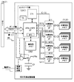
図1には、この発明に係る記憶装置の一実施例の概略構成図が示されている。この実施例の記憶装置は、HDDの置き換え製品として、記憶媒体にフラシュメモリを使用したSSD(Solid State Drive)に向けられている。記憶装置は、コントローラ部CONT、高速メモリRAM、フラシュメモリFLSH、及び内部バスBUS,IBUS1〜IBUSmから構成される。上記高速メモリRAMは、例えばシンクロナス・ダイナミック・ランダム・アクセス・メモリ(以下、SDRAMという)により構成される。この高速メモリRAMは、ブロックBLK1ないしBLKnのnブロックに分けられた記憶容量を有する。これらのブロックBLK1ないしBLKnは、特に制限されないが、128KB(キロバイト)のような記憶容量を持つ。 FIG. 1 shows a schematic configuration diagram of an embodiment of a storage device according to the present invention. The storage device of this embodiment is directed to an SSD (Solid State Drive) using a flash memory as a storage medium as a replacement product for an HDD. The storage device includes a controller unit CONT, a high-speed memory RAM, a flash memory FLSH, and internal buses BUS and IBUS1 to IBUSm. The high-speed memory RAM is composed of, for example, a synchronous dynamic random access memory (hereinafter referred to as SDRAM). This high-speed memory RAM has a storage capacity divided into n blocks of blocks BLK1 to BLKn. These blocks BLK1 to BLKn are not particularly limited, but have a storage capacity of 128 KB (kilobytes).
フラシュメモリFLSHは、m組に分けられたフラシュメモリFLSH1〜FLSHmから構成される。上記高速メモリRAMとm組に分けられたフラシュメモリFLSH1〜FLSHmとの間は、内部バスの一部を構成するm個の第2バスIBUS1〜IBUSmでデータ転送が行われる。これらの第2バスIBUS1〜IBUSmは、それぞれが独立して使用することが可能にされる。例えば、IBUS1〜IBUSmのうちいずれか1つを単独で使用することもできるし、IBUS1〜IBUSmを可変的に組み合わせて各々を同時に使用することが可能にされる。また、外部のホストHOSTから上記RAMにデータの書き込みを可能にする内部バスの他の一部を構成する第1バスBUSが設けられる。 The flash memory FLSH includes flash memories FLSH1 to FLSHm divided into m groups. Between the high-speed memory RAM and the flash memories FLSH1 to FLSHm divided into m groups, data transfer is performed by m second buses IBUS1 to IBUSm constituting a part of the internal bus. These second buses IBUS1 to IBUSm can be used independently. For example, any one of IBUS1 to IBUSm can be used alone, or each of IBUS1 to IBUSm can be variably combined and used simultaneously. In addition, a first bus BUS is provided which constitutes another part of the internal bus that enables data to be written from the external host HOST to the RAM.
上記コントラーラ部CONTは、第1動作と第2動作とを時分割的に同時に行うことが可能にされる。上記第1動作は、上記第1バスBUSを用いて外部のホストHOSTから上記高速メモリRAMに対してデータを書き込む動作である。上記第2動作は、上記高速メモリRAMに対する上記第1動作のための記憶領域を確保すべく、上記高速メモリRAMに格納されている記憶データのうち書き込み時の古い順であって、かかる記憶データのデータ量に対応して上記第2バスを用いて1ないしm個のブロック分を上記フラシュメモリに対して書き込む動作である。上記各バスBUS、IBIS1〜IBUSmのそれぞれ対応して、かかるバスを用いた動作に使用される制御信号を伝える制御線C,C1〜Cmがそれぞれが設けられる。 The controller unit CONT can perform the first operation and the second operation simultaneously in a time division manner. The first operation is an operation of writing data from the external host HOST to the high-speed memory RAM using the first bus BUS. The second operation is the oldest data at the time of writing among the stored data stored in the high-speed memory RAM in order to secure a storage area for the first operation with respect to the high-speed memory RAM. In this operation, 1 to m blocks are written into the flash memory using the second bus corresponding to the amount of data. Corresponding to each of the buses BUS and IBUS1 to IBUSm, control lines C and C1 to Cm for transmitting control signals used for operations using the buses are provided.
前記SDRAMのような高速メモリRAMは、HDDでのデータ書き込み速度や、フラシュメモリへのデータ書き込み速度に比べて十分に速い。このことを利用して、ホストからのデータ書き込みに必要な時間が割り当てられて上記第1バスを用いた高速メモリRAMへの書き込みや読み出しが可能にされる。これにより、コントローラ部は、上記時分割的に割り当てられた時間を利用して、ホストHOSTによる恒常的な書き込み動作や高速RAMに該当する記憶データが格納されていることを条件に恒常的な読み出し動作が確保される。 A high-speed memory RAM such as the SDRAM is sufficiently faster than the data writing speed in the HDD and the data writing speed in the flash memory. By utilizing this fact, a time required for data writing from the host is allocated, and writing to and reading from the high-speed memory RAM using the first bus is enabled. As a result, the controller unit uses the time allotted in a time-sharing manner to perform a constant read operation on condition that a constant write operation by the host HOST or stored data corresponding to the high-speed RAM is stored. Operation is ensured.
この実施例では、記憶媒体としての記憶容量がフラシュメモリFLSHの記憶容量で決定され、この実施例の記憶装置は、HDDとの置き換えあるいは互換を可能にすべくHDDに匹敵するような大きな記憶容量が設定される。上記高速メモリRAMの記憶容量は、上記フラシュメモリFLSHの記憶容量に比べて小さくされる。したがって、上記高速メモリRAMの記憶領域が満杯になると、それ以上の書き込みができなくなる。コントローラ部は、上記第1動作を恒常的に維持できるようにするために、上記高速メモリRAMに格納されている記憶データのうち書き込み時の古い順に記憶データをフラシュメモリFLSHに退避させて、外部のホストHOSTからの新たなデータ書き込むための記憶領域を確保する第2動作を実施する。 In this embodiment, the storage capacity as the storage medium is determined by the storage capacity of the flash memory FLSH, and the storage device of this embodiment has a large storage capacity comparable to the HDD so as to be able to replace or be compatible with the HDD. Is set. The storage capacity of the high-speed memory RAM is made smaller than the storage capacity of the flash memory FLSH. Therefore, when the storage area of the high-speed memory RAM becomes full, no further writing can be performed. In order to maintain the first operation constantly, the controller unit saves the stored data stored in the high-speed memory RAM in the flash memory FLSH in the order of the oldest data at the time of writing. A second operation for securing a storage area for writing new data from the host HOST is performed.
上記第2動作は、上記高速メモリRAMに対するメモリアクセス可能な時間のうち上記第1動作により使用された残り時間が割り当てられる。これにより、高速メモリRAMに対して、上記第1動作及び第2動作を時分割的に行われることにより、高速RAMに対して外部からのメモリアクセスとフラシュメモリへのデータ退避とを同時に実施することができる。上記第2動作の前提として、フラシュメモリFLSHは、消去状態であることが必要である。それ故、フラシュメモリFLSHでは、退避先に書き込みデータをあるときには、消去動作が実施される。したがって、フラシュメモリFLSHは、上記高速メモリRAMのブロックサイズに対応して消去単位サイズを決めることが便利である。消去単位サイズは、上記ブロックサイズの整数分の1であっても、整数倍分を同時に消去すればよいので構わない。 In the second operation, the remaining time used by the first operation is allocated to the memory accessible time for the high-speed memory RAM. Thus, the first operation and the second operation are performed on the high-speed memory RAM in a time-sharing manner, so that external memory access and data saving to the flash memory are simultaneously performed on the high-speed RAM. be able to. As a premise of the second operation, the flash memory FLSH needs to be in an erased state. Therefore, in the flash memory FLSH, an erase operation is performed when there is write data at the save destination. Therefore, it is convenient for the flash memory FLSH to determine the erase unit size corresponding to the block size of the high-speed memory RAM. Even if the erase unit size is 1 / integer of the block size, an integral multiple may be erased simultaneously.
上記第2動作は、例えば高速メモリRAMの書き込み可能な記憶領域のブロック数が最低値になると、第1動作とは無関係に書き込み時の古い順の記憶データが含まれるブロックの記憶データをフラシュメモリFLSHに退避させる。このとき、連続する一連のデータが複数ブロックに跨がって存在するときには、複数ブロック分が同時に退避される。つまり、第2バスは、IBIS1ないしIBUSmのようにm個存在するので、最大mブロック分が同時にフラシュメモリFLSHに転送される。上記退避される連続データが小さく、1つのブロック内であるときには、例えば1つのバスIBUS1を用いて1ブロック分がフラシュメモリFLSHに退避させられる。この構成は、フラシュメモリFLSHにおける書き換え回数を低減する上で有益である。 In the second operation, for example, when the number of blocks in the writable storage area of the high-speed memory RAM becomes the minimum value, the storage data of the block including the oldest storage data at the time of writing is stored in the flash memory regardless of the first operation. Retreat to FLSH. At this time, when a continuous series of data exists across a plurality of blocks, a plurality of blocks are simultaneously saved. In other words, since there are m second buses such as IBUS1 to IBUSm, the maximum m blocks are simultaneously transferred to the flash memory FLSH. When the continuous data to be saved is small and within one block, for example, one block is saved in the flash memory FLSH using one bus IBUS1. This configuration is useful for reducing the number of rewrites in the flash memory FLSH.
上記第2動作は、例えば高速メモリRAMの書き込み可能な記憶領域のブロック数が最低値以上であっても、第1動作による書き込む要求のデータ量が上記最低値より大きいときには、かかる第1動作に対応して第2動作が実施される。この場合、大量のデータを書き込む記憶領域を単時間で確保する必要から、上記連続する一連のデータが複数ブロックに跨がって存在するときには、複数ブロック分を同時に退避し、データバスに余りがあるときには、次に古い記憶データを合わせて退避させる。つまり、最大m個分のデータを退避するよう退避データを選択する。 For example, even if the number of blocks in the writable storage area of the high-speed memory RAM is equal to or greater than the minimum value, the second operation is performed when the amount of data requested for writing in the first operation is larger than the minimum value. Correspondingly, the second operation is performed. In this case, since it is necessary to secure a storage area for writing a large amount of data in a single time, when the continuous series of data exists across a plurality of blocks, a plurality of blocks are saved at the same time, and there is a remainder on the data bus. In some cases, the next oldest stored data is saved together. That is, the save data is selected so as to save the maximum m pieces of data.
例えば、上記m=4であって、1ブロックBLKが256セクタ(128KB)であるとき、1ないし4ブロックの任意量連続論理アドレスデータを一度に転送することが可能にされる。例えば、連続論理アドレス退避データが上記256セクタ分なら1ブロック分が転送され、連続論理アドレス退避データが上記512セクタ分なら2ブロック分が同時に転送されて、上記1ブロック分の転送と同じ時間内に転送される。仮に、高速メモリRAMとフラシュメモリFLSHとの間の内部バスを固定的に使用する構成では、この内部バスでの転送量に合わせてデータ退避が行われる。したがって、上記内部バスIBUS1〜IBUS4を設けた場合には、上記4ブロック単位でのデータ退避となり、上記1ブロック分のデータ退避でもよいときにも、4ブロック分のデータ退避が行われてしまう。この結果、フラシュメモリFLSHでの書き換え回数が増大してしまうが、この実施例のように各バスを退避データ量に応じて独立して使用できる構成では、上記フラシュメモリFLSHでの書き換え回数を低減できる。 For example, when m = 4 and 1 block BLK is 256 sectors (128 KB), it is possible to transfer 1 to 4 blocks of an arbitrary amount of continuous logical address data at a time. For example, if the continuous logical address save data is for 256 sectors, one block is transferred, and if the continuous logical address save data is for 512 sectors, two blocks are transferred at the same time as the transfer for the one block. Forwarded to In the configuration in which the internal bus between the high-speed memory RAM and the flash memory FLSH is fixedly used, data is saved according to the transfer amount of the internal bus. Therefore, when the internal buses IBUS1 to IBUS4 are provided, data is saved in units of the four blocks, and even when data for the one block may be saved, data for four blocks is saved. As a result, the number of rewrites in the flash memory FLSH increases. However, in the configuration in which each bus can be used independently according to the saved data amount as in this embodiment, the number of rewrites in the flash memory FLSH is reduced. it can.
上記第2バスの独立使用は、高速メモリRAMにおける不連続論理アドレスデータのフラシュメモリFLSHへの同時格納を可能にできる。例えば、ハードデスク内の全てのセクタに通し番号を振り、その通し番号によってセクタを指定するアドレス方式であるLBA(Logical Blook Addressing) 0x0000を先頭アドレスとする1ブロック分、LBA0x0500を先頭アドレスとする1ブロック分、LBA0x0A00を先頭アドレスとする1ブロック分、LBA0x0F00を先頭アドレスとする1ブロック分の計4ブロック分を同時にフラシュメモリFLSHに退避させることができる。このような不連続論理アドレスデータの組み合わせは、1ブロック分が2個で2ブロック分が1個の組み合わせ、1ブロックが1個で、3ブロック分が1個の組み合わせにより以下のように7通り存在する。つまり、(1, 1,1,1)、(1,1,2)、(1,2,1)、(2,1,1)、(1,3),(3,1)である。括弧内の数字1〜3は、ブロック数を表している。 The independent use of the second bus can simultaneously store discontinuous logical address data in the flash memory FLSH in the high-speed memory RAM. For example, a serial number is assigned to all sectors in the hard disk, and one block with LBA (Logical Blook Addressing) 0x0000, which is an address system for designating a sector by the serial number, and one block with LBA 0x0500 as the top address Thus, a total of four blocks, one block having LBA0x0A00 as the head address and one block having LBA0x0F00 as the head address, can be simultaneously saved in the flash memory FLSH. There are 7 combinations of such discontinuous logical address data by combining 1 block with 2 blocks and 2 blocks with 1 block, 1 block with 1 block, and 3 blocks with 1 block. Exists. That is, (1, 1, 1, 1), (1, 1, 2), (1, 2, 1), (2, 1, 1), (1, 3), (3, 1). Numbers 1 to 3 in parentheses represent the number of blocks.
図2には、この発明に係る記憶装置の他の一実施例の概略構成図が示されている。この実施例の高速メモリRAMは、ブロックBLK1ないしBLKmを1組として、p組が設けられる。この場合の前記図1のnは、n=m×pの関係とされる。これら各組のブロックBLK1ないしBLKmは、特に制限されないが、それぞれが前記同様に256セクタ(128KB)のような記憶容量を持つ。 FIG. 2 shows a schematic configuration diagram of another embodiment of the storage device according to the present invention. The high-speed memory RAM of this embodiment is provided with p sets, each of which includes blocks BLK1 to BLKm. In this case, n in FIG. 1 has a relationship of n = m × p. These sets of blocks BLK1 to BLKm are not particularly limited, but each has a storage capacity of 256 sectors (128 KB) as described above.
この構成では、前記図1の実施例のようにブロック単位での第2動作を実施できることの他、上記組単位での第2動作を実施することができる。つまり、コントローラ部は、退避データ量が大きいときには、逐一ブロックBLKと、それに対応したバスの組み合わせを指定することなく、上記p組のうちの1つの組を指定するだけで、m=4のときには自動的に前記4つの連続したブロックと4つのバスIBUS1〜IBUS4を選択することができる。 In this configuration, the second operation in units of blocks can be performed in addition to the second operation in units of blocks as in the embodiment of FIG. That is, when the amount of saved data is large, the controller unit only specifies one set of the p sets without specifying the combination of the block BLK and the corresponding bus, and when m = 4. The four consecutive blocks and the four buses IBUS1 to IBUS4 can be automatically selected.
コントローラ部は、上記高速メモリRAMに対して1〜p組の区分動作を処理する。各区分の動作モードは、転送/待機/格納であり、ホストHOSTからのデータの書き込みのために1区分以上を確保する仕組み(スケジューリング)を有する。滞りなく各動作を行うためには、例えば、高速メモリRAMの1ないしp組のうち、例えば第1組がフラシュメモリFLSHへのデータ転送を行うとき、第2組がフラシュメモリFLSHへの転送待機中で、第3組がホストHOSTからのデータの格納中のモデルが考えられる。したがって、上記p組は、3が最小構成値となる。 The controller unit processes 1 to p groups of segmenting operations for the high-speed memory RAM. The operation mode of each section is transfer / standby / storage, and has a mechanism (scheduling) for securing one or more sections for writing data from the host HOST. In order to perform each operation without delay, for example, when the first set performs data transfer to the flash memory FLSH among the 1 to p sets of the high-speed memory RAM, the second set waits for transfer to the flash memory FLSH. Among them, a model in which the third set is storing data from the host HOST can be considered. Therefore, 3 is the minimum configuration value in the above-described p set.
図3には、この発明に係る記憶装置の一実施例の概略ブロック図が示されている。この実施例の記憶装置は、記憶媒体にフラシュメモリ(FLSH)を使用したSSD(Solid State Drive)として、特に制限されないが、1024Mビットの記憶容量を持つ2値又は多値(4値)フラッシュメモリを、多数個を1つのパッケージの中に搭載してHDDと置き換え可能な記憶容量を持つようにされる。 FIG. 3 is a schematic block diagram showing an embodiment of the storage device according to the present invention. The storage device of this embodiment is not particularly limited as an SSD (Solid State Drive) using a flash memory (FLSH) as a storage medium, but is a binary or multi-level (4-level) flash memory having a storage capacity of 1024 Mbits. Are installed in a single package to have a storage capacity that can replace the HDD.
これら多数個の不揮発性メモリ(FLSH)は、特に制限されないが、4組に分割されて、それぞれ不揮発性メモリI/F(インターフェイス)を通して前記第2バスとしての内部バスIBUS1〜IBUS4に接続される。前記第1バスとしての内部バスBUSは、例えばATA又はSCSIのようなインターフェイスI/Fを有するコントローラ部に接続される。上記コントローラ部は、CPUで示したような1チップマイクロコンピュータ等のようなコントローラと上記ATA(AT Attachment)又はSCSI(Small Computer System Interface) のようなインターフェイスI/Fとから構成される。したがって、コントローラ部は、不揮発性メモリインターフェイスI/Fに設けられたドライバと上記不揮発性メモリ(FLSH)との間でデータのやりとり、つまりはデータの書き込みや読み出しを行う。 These many non-volatile memories (FLSH) are not particularly limited, but are divided into four groups and are connected to the internal buses IBUS1 to IBUS4 as the second bus through the non-volatile memories I / F (interfaces), respectively. . The internal bus BUS as the first bus is connected to a controller unit having an interface I / F such as ATA or SCSI. The controller section includes a controller such as a one-chip microcomputer as indicated by a CPU and an interface I / F such as ATA (AT Attachment) or SCSI (Small Computer System Interface). Therefore, the controller unit exchanges data between the driver provided in the nonvolatile memory interface I / F and the nonvolatile memory (FLSH), that is, writes and reads data.
上記コントローラ部は、揮発性メモリ(RAM)とのインターェイス部にマルチプレクサMPXを有しており、このマルチプレクサMPXの切り替えにより、前記ホストHOSTからのアクセスと、揮発性メモリ(RAM)内のデータ退避のためのアクセスとが時分割的に同時動作が可能にされる。 The controller unit has a multiplexer MPX in an interface unit with a volatile memory (RAM), and by switching the multiplexer MPX, access from the host HOST and data saving in the volatile memory (RAM) are performed. Access to the network is enabled in a time-sharing manner.
上記フラシュメモリFLSHからのデータ読み出しは、書き込み動作に比べて高速にできるので、もしも揮発性メモリ(RAM)に該当する論理アドレスのデータが存在しない場合にも、揮発性メモリ(RAM)からの読み出し動作と同等にフラシュメモリFLSHから上記ATA又はSCSIのようなインターフェイスI/Fとデータ線(第1バス)を通してホストHOSTに読み出すことができる。このため、前記図1、図2の実施例では省略されているが、フラシュメモリFLSHからホストHOSTに向けてデータを読み出す信号経路が上記コントローラ部CONTに設けられるものである。コントローラ部CONTに設けられたテーブルTBLは、前記揮発性メモリ(高速メモリ)RAMのデータ退避のスケジューリングに利用される論理アドレス等が格納されている。 Since the data read from the flash memory FLSH can be performed faster than the write operation, even if there is no logical address data in the volatile memory (RAM), the read from the volatile memory (RAM) is possible. Similar to the operation, the data can be read from the flash memory FLSH to the host HOST through the interface I / F such as ATA or SCSI and the data line (first bus). Therefore, although omitted in the embodiments of FIGS. 1 and 2, a signal path for reading data from the flash memory FLSH to the host HOST is provided in the controller unit CONT. The table TBL provided in the controller unit CONT stores logical addresses and the like used for scheduling data saving in the volatile memory (high-speed memory) RAM.
この実施例では、上記パッケージには、特に制限されないが、電源検出回路と電源遮断時の動作電圧を確保するためのコンデンサCP及びスイッチSWを更に備えている。このコンデンサCPは、システム側において予期しない電源遮断が生じた場合でも、その蓄積電荷によって不揮発性メモリやコントローラ部及び揮発性メモリや電源検出回路に電圧を供給して、不揮発性メモリの中断処理を含めた正常終了状態まで動作電圧を維持するように動作する。上記のような中断処理が行われるような動作電圧確保のために、セラミックコンデンサもしくは電気二重層コンデンサを複数個並列して例えば約数百μFから数十mF程度の容量値を持つようにされる。 In this embodiment, the package is further provided with a power detection circuit and a capacitor CP and a switch SW for securing an operating voltage when the power is shut off, although not particularly limited. The capacitor CP supplies a voltage to the nonvolatile memory, the controller unit, the volatile memory, and the power detection circuit by the accumulated charge even when the power supply is unexpectedly shut down on the system side, so that the nonvolatile memory is interrupted. It operates so as to maintain the operating voltage until the normal end state is included. In order to secure an operating voltage such that the above interruption processing is performed, a plurality of ceramic capacitors or electric double layer capacitors are arranged in parallel so as to have a capacitance value of about several hundred μF to several tens of mF, for example. .
上記電源検出回路は、マイクロコンピュータ等のようなホスト側からの電源電圧Vccを受けて、その電源投入と電源遮断を検出する。この検出信号は、ゲート回路Gの一方の入力に供給される。このゲート回路Gの他方の入力にはコントロール線を通したコントロール信号が供給される。ゲート回路Gは、例えばナンド(NAND)ゲート回路のような論理回路からなり、電源投入又は電源遮断に対応したコントローラ部からの信号、あるいはコントロール線から供給される制御信号に対応してスイッチSWの制御等を行う。 The power supply detection circuit receives the power supply voltage Vcc from the host side such as a microcomputer and detects the power-on and power-off. This detection signal is supplied to one input of the gate circuit G. A control signal through a control line is supplied to the other input of the gate circuit G. The gate circuit G is composed of a logic circuit such as a NAND gate circuit, for example. The gate circuit G has a switch SW corresponding to a signal from a controller corresponding to power-on or power-off or a control signal supplied from a control line. Control and so on.
スイッチSWは、ゲート回路Gの出力信号によって切り替えられ、コンデンサCPが電源Vccによる充電動作から、その保持電圧を記憶装置SSDの内部回路の動作電圧として供給する動作を行う。上記電源検出回路は、上記コンデンサCPの保持電圧が有効に利用できるようにするために、コンデンサCPで形成された動作電圧がシステム側に逆流してしまうのを防止するような機能も持つものである。最も簡単な構成は、ダイオード等の一方向性素子を通してシステム側からの電源電圧Vccが、記憶装置SSDの電源電圧として上記スイッチSWを通してコンデンサCPにチャージアップされるとともに、コントロール部、不揮発性メモリ(フラシュメモリFLSH)、揮発性メモリ(高速メモリRAM)、インターフェイス回路I/F及び電源検出回路に伝えられる。 The switch SW is switched by the output signal of the gate circuit G, and the capacitor CP performs an operation of supplying the held voltage as an operating voltage of the internal circuit of the storage device SSD from the charging operation by the power source Vcc. The power supply detection circuit also has a function of preventing the operating voltage formed by the capacitor CP from flowing back to the system side so that the holding voltage of the capacitor CP can be used effectively. is there. In the simplest configuration, the power supply voltage Vcc from the system side is charged to the capacitor CP through the switch SW as the power supply voltage of the storage device SSD through a unidirectional element such as a diode, and the control unit, nonvolatile memory ( Flash memory FLSH), volatile memory (high-speed memory RAM), interface circuit I / F, and power supply detection circuit.
上記記憶装置SSDは、例えば2.5インチのハードディスクドライブ装置と同様な外形サイズ(70.0×100.0×9.5mm)又は3.5インチのハードディスクドライブ装置と同様な外形サイズ(101.6×146.0×25.4mm)のパッケージに搭載され、インターフェイス回路INFに接続されるコネクタピンも上記2.5インチのハードディスクドライブ装置又は3.5インチのハードディスクドライブ装置と同様なものが用いられる。これにより、この実施例の記憶装置SSDは、HDD(ハードディスクドライブ)互換性記憶装置とされる。 The storage device SSD has, for example, the same outer size (70.0 × 100.0 × 9.5 mm) as that of a 2.5-inch hard disk drive device or the same outer size (101. 6 × 146.0 × 25.4 mm), and the connector pin connected to the interface circuit INF is the same as the 2.5 inch hard disk drive device or the 3.5 inch hard disk drive device. It is done. Thus, the storage device SSD of this embodiment is an HDD (Hard Disk Drive) compatible storage device.
この実施例の記憶装置SSDにおいては、電源検出回路によって電源遮断を検出したときの動作中の取扱いは、正常動作完了させるまで待つ場合と、動作中断させる場合が選択できる。これは、動作中の処理内容、そのメモリコントローラ部による揮発性メモリから不揮発性メモリに書き込むデータ量(所要時間)および電源再投入時の継続可否などから決められる。 In the storage device SSD of this embodiment, the handling during the operation when the power cut-off is detected by the power detection circuit can be selected to wait until the normal operation is completed or to interrupt the operation. This is determined based on the processing contents during operation, the amount of data written from the volatile memory to the nonvolatile memory by the memory controller unit (required time), and whether or not to continue when the power is turned on again.
以上本発明者によってなされた発明を、前記実施形態に基づき具体的に説明したが、本発明は、前記実施形態に限定されるものではなく、その要旨を逸脱しない範囲において種々変更可能である。例えば、揮発性メモリは、例えば高速メモリRAMは、前記のようなSDRAMの他に、スタティック型RAMであってもよい。フラッシュメモリは、NAND型フラッシュメモリの他にNOR型のフラッシュメモリであってもよい。コントローラ部は、高速メモリRAMに対して前記時分割により複数のバスから同時アクセスできるようにするものであれば何であってもよい。 Although the invention made by the inventor has been specifically described based on the above embodiment, the present invention is not limited to the above embodiment, and various modifications can be made without departing from the scope of the invention. For example, the volatile memory, for example, the high-speed memory RAM may be a static RAM in addition to the SDRAM as described above. The flash memory may be a NOR flash memory in addition to the NAND flash memory. The controller unit may be anything as long as it enables simultaneous access to the high-speed memory RAM from a plurality of buses by the time division.
フラッシュメモリを用いて構成され、例えばハードディスクドライブメモリと置き換え可能な記憶装置等に広く利用できる。 It is configured using a flash memory and can be widely used for a storage device that can be replaced with a hard disk drive memory, for example.
CONT…コントローラ部、RAM…高速メモリ(揮発性メモリ)、BLK1〜BLKn…ブロック、FLSH(FLSH1〜m)…フラシュメモリ(不揮発性メモリ)、BUS…第1バス(内部バス)、IBUS1〜IBUSm…第2バス(内部バス)、HOST…ホスト、CPU…1チップマイクロコンピュータ、TBL…テーブル、SW…スイッチ、CP…コンデンサ、G…ゲート回路、 CONT: Controller unit, RAM: High speed memory (volatile memory), BLK1 to BLKn: Block, FLSH (FLSH1 to m) ... Flash memory (nonvolatile memory), BUS ... First bus (internal bus), IBUS1 to IBUSm ... Second bus (internal bus), HOST ... Host, CPU ... 1 chip microcomputer, TBL ... Table, SW ... Switch, CP ... Capacitor, G ... Gate circuit,
Claims (5)
一括消去型不揮発性メモリと、
上記半導体ランダム・アクセス・メモリ及び上記一括消去型不揮発性メモリに対して第1動作及び第2動作を含むメモリアクセスを行うコントローラ部と、
内部バスとを有し、
上記半導体ランダム・アクセス・メモリは、記憶領域が複数からなるn個のブロックに分けられ、
上記一括消去型不揮発性メモリは、複数のm組に分けられ、
上記内部バスは、
外部から上記半導体ランダム・アクセス・メモリに対してデータの書き込みが可能にされた第1バスと、
上記半導体ランダム・アクセス・メモリから前記m組に分けられた一括消去型不揮発性メモリに対してそれぞれ独立してデータの書き込みが可能にされたm個の第2バスとを有し、
上記コントローラ部は、
上記第1動作と上記第2動作とを時分割的に同時に行うことが可能にされ、
上記第1動作は、上記第1バスを用いて外部から上記半導体ランダム・アクセス・メモリに対してデータの書き込み、
第2動作は、上記半導体ランダム・アクセス・メモリに対する上記第1動作のための記憶領域を確保すべく、上記半導体ランダム・アクセス・メモリの記憶データのうち書き込み時の古い順であって、かかる記憶データのデータ量に対応して上記第2バスを用いて1ないしm個のブロック分を上記一括消去型不揮発性メモリに対して書き込む、
記憶装置 Semiconductor random access memory,
Batch erase nonvolatile memory,
A controller unit for performing memory access including a first operation and a second operation on the semiconductor random access memory and the batch erase nonvolatile memory;
An internal bus,
The semiconductor random access memory is divided into n blocks each having a plurality of storage areas.
The batch erase nonvolatile memory is divided into a plurality of m sets,
The internal bus
A first bus capable of writing data to the semiconductor random access memory from the outside;
And m second buses capable of independently writing data from the semiconductor random access memory to the batch erasable nonvolatile memory divided into the m groups,
The controller part
The first operation and the second operation can be performed simultaneously in a time-sharing manner,
The first operation is to write data to the semiconductor random access memory from the outside using the first bus.
The second operation is the oldest data at the time of writing in the storage data of the semiconductor random access memory in order to secure a storage area for the first operation for the semiconductor random access memory. Write 1 to m blocks to the batch erase nonvolatile memory using the second bus corresponding to the amount of data.
Storage device
上記一括消去型不揮発性メモリは、上記半導体ランダム・アクセス・メモリのブロック単位に対応した記憶領域毎の一括消去動作が可能にされる、
記憶装置。 In claim 1,
The batch erasing type nonvolatile memory enables a batch erasing operation for each storage area corresponding to a block unit of the semiconductor random access memory.
Storage device.
上記第2動作は、上記第2バスを用いて上記記憶データの書き込み時の古い複数順であって、上記最大m個のブロック分を上記一括消去型不揮発性メモリに対して書き込む動作を含む、
記憶装置。 In claim 1,
The second operation includes an operation of writing the maximum m blocks to the batch erasable nonvolatile memory in the old plural order when writing the stored data using the second bus.
Storage device.
上記半導体ランダム・アクセス・メモリの上記n個のブロックは、複数のp組に分けられ、各組には上記m個のブロックがそれぞれ割り当てられ、
上記第2動作は、m個のブロック単位で上記一括消去型不揮発性メモリに対して上記第2バスを用いて上記一括消去型不揮発性メモリに対して書き込む動作を含む、
記憶装置 In claim 1 or 2,
The n blocks of the semiconductor random access memory are divided into a plurality of p sets, and each of the m blocks is assigned to each set.
The second operation includes an operation of writing to the batch erase nonvolatile memory in the block erase nonvolatile memory in units of m blocks using the second bus.
Storage device
上記コントローラ部は、ホストとの間でのデータの入出力を行うHDD互換性のインターフェイス部とを更に備え、
上記半導体ランダム・アクセス・メモリ、一括消去型不揮発性メモリ、コントローラ部及び内部バスは、汎用小型ハードディスクドライブ装置に対応された外形サイズ及びコネクタピンを備えたパッケージに搭載される、
記憶装置。 In claims 1 to 4,
The controller unit further includes an HDD compatible interface unit for inputting / outputting data to / from the host,
The semiconductor random access memory, the batch erase nonvolatile memory, the controller unit and the internal bus are mounted in a package having an external size and a connector pin corresponding to a general-purpose small hard disk drive device.
Storage device.
Priority Applications (1)
| Application Number | Priority Date | Filing Date | Title |
|---|---|---|---|
| JP2008281957A JP2010108385A (en) | 2008-10-31 | 2008-10-31 | Storage device |
Applications Claiming Priority (1)
| Application Number | Priority Date | Filing Date | Title |
|---|---|---|---|
| JP2008281957A JP2010108385A (en) | 2008-10-31 | 2008-10-31 | Storage device |
Publications (2)
| Publication Number | Publication Date |
|---|---|
| JP2010108385A true JP2010108385A (en) | 2010-05-13 |
| JP2010108385A5 JP2010108385A5 (en) | 2012-01-12 |
Family
ID=42297749
Family Applications (1)
| Application Number | Title | Priority Date | Filing Date |
|---|---|---|---|
| JP2008281957A Pending JP2010108385A (en) | 2008-10-31 | 2008-10-31 | Storage device |
Country Status (1)
| Country | Link |
|---|---|
| JP (1) | JP2010108385A (en) |
Cited By (6)
| Publication number | Priority date | Publication date | Assignee | Title |
|---|---|---|---|---|
| WO2013168479A1 (en) * | 2012-05-07 | 2013-11-14 | 株式会社バッファローメモリ | Ssd (solid state drive) device |
| US9097747B2 (en) | 2010-12-24 | 2015-08-04 | Kabushiki Kaisha Toshiba | Electronic device, and capacitor capacitance detection method applied to the same |
| US9304952B2 (en) | 2010-10-21 | 2016-04-05 | Kabushiki Kaisha Toshiba | Memory control device, storage device, and memory control method |
| JP2016051472A (en) * | 2014-08-28 | 2016-04-11 | パナソニックIpマネジメント株式会社 | Memory card |
| JP2016181058A (en) * | 2015-03-23 | 2016-10-13 | 株式会社東芝 | Semiconductor memory device |
| JP2019016377A (en) * | 2018-09-11 | 2019-01-31 | 東芝メモリ株式会社 | Control method of semiconductor memory device |
Citations (5)
| Publication number | Priority date | Publication date | Assignee | Title |
|---|---|---|---|---|
| JP2001051896A (en) * | 1999-08-04 | 2001-02-23 | Hitachi Ltd | Storage device |
| JP2006252535A (en) * | 2005-02-09 | 2006-09-21 | Hitachi Ulsi Systems Co Ltd | Storage apparatus |
| JP2007517320A (en) * | 2003-12-30 | 2007-06-28 | サンディスク コーポレイション | Adaptive mode switching of flash memory address mapping based on host usage characteristics |
| JP2007280068A (en) * | 2006-04-06 | 2007-10-25 | Sony Corp | Flash memory device and access method to flash memory |
| JP2008135046A (en) * | 2007-12-21 | 2008-06-12 | Renesas Technology Corp | Memory system |
-
2008
- 2008-10-31 JP JP2008281957A patent/JP2010108385A/en active Pending
Patent Citations (5)
| Publication number | Priority date | Publication date | Assignee | Title |
|---|---|---|---|---|
| JP2001051896A (en) * | 1999-08-04 | 2001-02-23 | Hitachi Ltd | Storage device |
| JP2007517320A (en) * | 2003-12-30 | 2007-06-28 | サンディスク コーポレイション | Adaptive mode switching of flash memory address mapping based on host usage characteristics |
| JP2006252535A (en) * | 2005-02-09 | 2006-09-21 | Hitachi Ulsi Systems Co Ltd | Storage apparatus |
| JP2007280068A (en) * | 2006-04-06 | 2007-10-25 | Sony Corp | Flash memory device and access method to flash memory |
| JP2008135046A (en) * | 2007-12-21 | 2008-06-12 | Renesas Technology Corp | Memory system |
Cited By (7)
| Publication number | Priority date | Publication date | Assignee | Title |
|---|---|---|---|---|
| US9304952B2 (en) | 2010-10-21 | 2016-04-05 | Kabushiki Kaisha Toshiba | Memory control device, storage device, and memory control method |
| US9097747B2 (en) | 2010-12-24 | 2015-08-04 | Kabushiki Kaisha Toshiba | Electronic device, and capacitor capacitance detection method applied to the same |
| US9882410B2 (en) | 2010-12-24 | 2018-01-30 | Toshiba Memory Corporation | Electronic device, and capacitor capacitance detection method applied to the same |
| WO2013168479A1 (en) * | 2012-05-07 | 2013-11-14 | 株式会社バッファローメモリ | Ssd (solid state drive) device |
| JP2016051472A (en) * | 2014-08-28 | 2016-04-11 | パナソニックIpマネジメント株式会社 | Memory card |
| JP2016181058A (en) * | 2015-03-23 | 2016-10-13 | 株式会社東芝 | Semiconductor memory device |
| JP2019016377A (en) * | 2018-09-11 | 2019-01-31 | 東芝メモリ株式会社 | Control method of semiconductor memory device |
Similar Documents
| Publication | Publication Date | Title |
|---|---|---|
| US10915475B2 (en) | Methods and apparatus for variable size logical page management based on hot and cold data | |
| US8606987B2 (en) | Data writing method for flash memory and controller using the same | |
| US8504762B2 (en) | Flash memory storage device with data interface | |
| US10379782B2 (en) | Host managed solid state drivecaching using dynamic write acceleration | |
| JP5728672B2 (en) | Hybrid memory management | |
| JP4844639B2 (en) | MEMORY CONTROLLER, FLASH MEMORY SYSTEM HAVING MEMORY CONTROLLER, AND FLASH MEMORY CONTROL METHOD | |
| US8001317B2 (en) | Data writing method for non-volatile memory and controller using the same | |
| US8055873B2 (en) | Data writing method for flash memory, and controller and system using the same | |
| US9128618B2 (en) | Non-volatile memory controller processing new request before completing current operation, system including same, and method | |
| TWI385519B (en) | Data writing method, and flash storage system and controller using the same | |
| JP2000067574A (en) | Semiconductor memory | |
| CN111158579B (en) | Solid state disk and data access method thereof | |
| US8037236B2 (en) | Flash memory writing method and storage system and controller using the same | |
| US20200089603A1 (en) | Operating method of memory system and memory system | |
| US11334272B2 (en) | Memory system and operating method thereof | |
| JP2006252535A (en) | Storage apparatus | |
| JP2010108385A (en) | Storage device | |
| JP2011070365A (en) | Memory system | |
| JP5259257B2 (en) | Storage device | |
| TWI790628B (en) | Memory system and control method | |
| CN110727470B (en) | Hybrid nonvolatile memory device | |
| JP2009175877A (en) | Semiconductor memory | |
| EP3772682A1 (en) | Method and apparatus to improve write bandwidth of a block-based multi-level cell non-volatile memory | |
| JP2010152778A (en) | Semiconductor storage device | |
| JP2010026950A (en) | Storage device |
Legal Events
| Date | Code | Title | Description |
|---|---|---|---|
| A621 | Written request for application examination |
Free format text: JAPANESE INTERMEDIATE CODE: A621 Effective date: 20111019 |
|
| A521 | Written amendment |
Free format text: JAPANESE INTERMEDIATE CODE: A523 Effective date: 20111118 |
|
| A977 | Report on retrieval |
Free format text: JAPANESE INTERMEDIATE CODE: A971007 Effective date: 20130417 |
|
| A131 | Notification of reasons for refusal |
Free format text: JAPANESE INTERMEDIATE CODE: A131 Effective date: 20130508 |
|
| A02 | Decision of refusal |
Free format text: JAPANESE INTERMEDIATE CODE: A02 Effective date: 20131002 |