JP2010062986A - Mounting structure for noise-proof component - Google Patents
Mounting structure for noise-proof component Download PDFInfo
- Publication number
- JP2010062986A JP2010062986A JP2008228258A JP2008228258A JP2010062986A JP 2010062986 A JP2010062986 A JP 2010062986A JP 2008228258 A JP2008228258 A JP 2008228258A JP 2008228258 A JP2008228258 A JP 2008228258A JP 2010062986 A JP2010062986 A JP 2010062986A
- Authority
- JP
- Japan
- Prior art keywords
- noise
- insulator
- input
- electrode
- mounting structure
- Prior art date
- Legal status (The legal status is an assumption and is not a legal conclusion. Google has not performed a legal analysis and makes no representation as to the accuracy of the status listed.)
- Pending
Links
Images


Abstract
Description
この発明は、信号配線上に侵入したノイズを除去するためのノイズ対策部品の実装構造に関するものである。 The present invention relates to a mounting structure of a noise countermeasure component for removing noise that has entered a signal wiring.
携帯電話等の無線通信機器における受信感度劣化を防止するためには、配線基板の信号配線上に侵入したノイズを有効に除去することが必要である。
このようなノイズを除去する技術としては、例えば、無線通信機器においては、通信に使用する周波数帯において挿入損失が大きなノイズ対策部品であるノイズフィルタを、ノイズが重畳した信号配線上に実装する方法がある。
そして、このようにノイズ対策部品を実装する構造としては、例えば、特許文献1に開示の技術がある。
この技術は、インダクタやコンデンサを積層したノイズフィルタにおいて、コンデンサが配線基板側に位置するように、ノイズフィルタを配線基板に実装することにより、コンデンサ電極である接地端子電極と配線基板の接地パターン間の距離を最小にしたものである。
このような構造にすることで、コンデンサ電極から配線基板上の接地用ランド間の距離を短くすることができる。その結果、コンデンサ電極から接地用ランド間に発生するインピーダンス(インダクタンス)を低減して、ノイズフィルタの挿入損失の劣化を抑えるようにしている。
In order to prevent reception sensitivity deterioration in a wireless communication device such as a cellular phone, it is necessary to effectively remove noise that has entered the signal wiring on the wiring board.
As a technique for removing such noise, for example, in a wireless communication device, a method of mounting a noise filter, which is a noise countermeasure component having a large insertion loss in a frequency band used for communication, on a signal wiring on which noise is superimposed There is.
And as a structure which mounts a noise countermeasure component in this way, there exists a technique disclosed by
In this technology, in a noise filter in which inductors and capacitors are laminated, the noise filter is mounted on the wiring board so that the capacitor is located on the wiring board side, so that the ground terminal electrode that is the capacitor electrode and the ground pattern of the wiring board The distance is minimized.
With this structure, the distance between the capacitor electrode and the grounding land on the wiring board can be shortened. As a result, the impedance (inductance) generated between the capacitor electrode and the grounding land is reduced to suppress the deterioration of the insertion loss of the noise filter.
しかし、上記した従来の技術では、次のような問題がある。
上記したノイズ対策部品の実装構造では、ノイズに対する挿入損失、すなわち、ノイズ透過率を小さくすることができるが、ノイズ反射率を小さくすることができない。
つまり、携帯電話のように機器内のノイズ干渉に弱いシステム内においては、ノイズフィルタで反射されたノイズも機器の性能に大きな影響を与える。このため、ノイズによる機器内のトラブルを確実に防止するためには、ノイズ対策部品において、ノイズを減衰させるだけでなく、当該ノイズ対策部品におけるノイズの反射率をも抑える必要がある。
しかしながら、上記した従来のノイズ対策部品の実装構造では、ノイズの反射率を小さくするための対策がとられておらず、ノイズを十分に除去することができない。
However, the conventional techniques described above have the following problems.
In the mounting structure of the noise countermeasure component described above, the insertion loss with respect to noise, that is, the noise transmittance can be reduced, but the noise reflectance cannot be reduced.
That is, in a system that is vulnerable to noise interference in a device such as a mobile phone, the noise reflected by the noise filter also greatly affects the performance of the device. Therefore, in order to surely prevent troubles in the equipment due to noise, it is necessary not only to attenuate the noise in the noise countermeasure component but also to suppress the noise reflectivity in the noise countermeasure component.
However, in the above-described conventional mounting structure for noise countermeasure components, no measures are taken to reduce the reflectance of noise, and noise cannot be sufficiently removed.
この発明は、上述した課題を解決するためになされたもので、ノイズ透過率を小さくすることができるだけでなく、ノイズ反射率をも小さくすることもできるノイズ対策部品の実装構造を提供することを目的とする。 The present invention has been made to solve the above-described problems, and provides a mounting structure for a noise countermeasure component that not only can reduce the noise transmittance but also can reduce the noise reflectance. Objective.
上記課題を解決するために、請求項1の発明は、絶縁体と、下端の入力側引き出し電極を絶縁体の前面に露出させると共に出力側引き出し電極を後面に露出させた状態でこの絶縁体内に横並びに収納されたn数のコイル体と、絶縁体の前面に設けられ且つn数の入力側引き出し電極にそれぞれ電気的に接続されたn数の入力側外部電極と、絶縁体の後面に設けられ且つn数の出力側引き出し電極にそれぞれ電気的に接続されたn数の出力側外部電極とを有したノイズ対策部品を、配線基板の信号配線上に実装するノイズ対策部品の実装構造であって、各コイル体の各入力側引き出し電極を、絶縁体の下面に対して平行に引き出し、ノイズ対策部品が実装される配線基板上の領域に、1つの平面導体をn数の入力側引き出し電極と対向するように配設した構成とする。
かかる構成により、ノイズ対策部品を、配線基板の信号配線上に実装すると、ある信号配線に侵入したノイズは、その信号配線に入力側外部電極を通じて接続されている入力側引き出し電極に入力される。そして、ノイズは、その入力側引き出し電極のコイル体によって減衰され、出力側引き出し電極から出力側外部電極を通じて、信号配線上に僅かに出力される。したがって、このノイズ対策部品によるノイズ透過率は非常に小さい。
ところで、当該信号配線に侵入したノイズの一部が、入力側外部電極から入力側引き出し電極に入力した後、この電極で反射され、元の信号配線上に戻り、他の機器に悪影響を与えるおそれがある。
しかしながら、この発明のノイズ対策部品の実装構造では、各コイル体の各入力側引き出し電極が、絶縁体の下面に対して平行に引き出され、ノイズ対策部品が実装された配線基板上の領域に、平面導体が入力側引き出し電極と対向するように配設されているので、各入力側引き出し電極と平面導体との間に、容量が発生する。そして、1つの平面導体がn数の入力側引き出し電極に対向しているので、n数の入力側引き出し電極同士が、入力側引き出し電極と平面導体との間の容量によって、接続された状態になる。この結果、上記信号配線から上記入力側引き出し電極内に侵入したノイズは、上記容量を通じて他の入力側引き出し電極に入り、他のコイル体内に送り込まれ、そのインダクタンスによって減衰される。
このようにして、上記ある信号配線から上記入力側引き出し電極に入力したノイズは、この電極で反射されることなく、他のコイル体で減衰されるので、ノイズの反射量は非常に少なくなる。
In order to solve the above problems, the invention of
With this configuration, when the noise countermeasure component is mounted on the signal wiring of the wiring board, the noise that has entered the signal wiring is input to the input-side lead electrode connected to the signal wiring through the input-side external electrode. Then, the noise is attenuated by the coil body of the input side extraction electrode, and is slightly output from the output side extraction electrode to the signal wiring through the output side external electrode. Therefore, the noise transmittance by this noise countermeasure component is very small.
By the way, a part of the noise that has entered the signal wiring is input from the input-side external electrode to the input-side extraction electrode, then reflected by this electrode, returns to the original signal wiring, and may adversely affect other devices. There is.
However, in the mounting structure of the noise countermeasure component of the present invention, each input-side lead electrode of each coil body is pulled out parallel to the lower surface of the insulator, and in the region on the wiring board on which the noise countermeasure component is mounted, Since the planar conductor is disposed so as to face the input-side extraction electrode, a capacitance is generated between each input-side extraction electrode and the planar conductor. Since one planar conductor faces n input-side extraction electrodes, the n number of input-side extraction electrodes are connected to each other by the capacitance between the input-side extraction electrode and the planar conductor. Become. As a result, noise that has entered the input-side extraction electrode from the signal wiring enters the other input-side extraction electrode through the capacitor, is sent into another coil body, and is attenuated by the inductance.
In this way, noise input from the signal wiring to the input-side extraction electrode is attenuated by another coil body without being reflected by this electrode, so that the amount of reflected noise is very small.
請求項2の発明は、請求項1に記載のノイズ対策部品の実装構造において、全てのコイル体を、絶縁体の上下方向に向けて絶縁体内に収納すると共に、配線基板上の平面導体の大きさを、当該平面導体が全てのコイル体の下端面と対向する大きさに設定した構成とする。
かかる構成により、絶縁体の上下方向に向けて絶縁体内に収納されたコイル体から発生した磁界が、コイル体の下端面と対向する平面導体によって、遮蔽される。
According to a second aspect of the present invention, in the mounting structure of the noise countermeasure component according to the first aspect, all the coil bodies are accommodated in the insulator in the vertical direction of the insulator, and the size of the planar conductor on the wiring board is increased. The size is set so that the planar conductor faces the lower end surfaces of all the coil bodies.
With this configuration, the magnetic field generated from the coil body housed in the insulator in the vertical direction of the insulator is shielded by the flat conductor facing the lower end surface of the coil body.
請求項3の発明は、請求項1又は請求項2に記載のノイズ対策部品の実装構造において、平面導体を、非接地状態にした構成とする。
かかる構成により、平面導体を、非接地状態にしたので、各入力側引き出し電極と平面導体との間に生じる容量を大きくすることができる。
According to a third aspect of the present invention, in the noise countermeasure component mounting structure according to the first or second aspect, the planar conductor is in a non-grounded state.
With such a configuration, since the planar conductor is not grounded, the capacitance generated between each input-side extraction electrode and the planar conductor can be increased.
請求項4の発明は、請求項1ないし請求項3のいずれかに記載のノイズ対策部品の実装構造において、各コイル体の出力側引き出し電極の途中部に一方端が接続され且つ他方端が絶縁体の側面に露出したコンデンサを絶縁体内に設けると共に、当該コンデンサの他方端に電気的に接続するグランド用外部電極を絶縁体の側面に設けることで、ノイズ対策部品内にn数のL型フィルタを構成し、グランド用外部電極を上記配線基板上に設けたグランド配線に接続した構成とする。
かかる構成により、信号配線から入力側外部電極を通じて入力側引き出し電極に入力されたノイズは、その入力側引き出し電極のコイル体によって減衰される。そして、このコイル体から出力側引き出し電極側に出力されたノイズは、出力側引き出し電極の途中部に接続されたコンデンサに入力し、グランド用外部電極を通じてグランド配線上に流出する。
According to a fourth aspect of the present invention, in the noise countermeasure component mounting structure according to any one of the first to third aspects, one end is connected to an intermediate portion of the output-side lead electrode of each coil body and the other end is insulated. A capacitor exposed on the side surface of the body is provided in the insulator, and an external ground electrode that is electrically connected to the other end of the capacitor is provided on the side surface of the insulator. The ground external electrode is connected to the ground wiring provided on the wiring board.
With this configuration, noise input from the signal wiring to the input-side extraction electrode through the input-side external electrode is attenuated by the coil body of the input-side extraction electrode. The noise output from the coil body to the output-side extraction electrode is input to a capacitor connected to the middle portion of the output-side extraction electrode, and flows out to the ground wiring through the ground external electrode.
請求項5の発明は、請求項1ないし請求項3のいずれかに記載のノイズ対策部品の実装構造において、各コイル体の出力側端部に各入力側端部が接続され且つ各出力側引き出し電極が絶縁体の後面に露出された別体のコイル体を絶縁体内に設け、当該各出力側引き出し電極を、絶縁体の下面に対して平行に引き出して、出力側外部電極をこの出力側引き出し電極に電気的に接続し、且つコイル体と別体のコイル体との接続部に一方端が接続され且つ他方端が絶縁体の側面に露出したコンデンサを絶縁体内に設けると共に、当該コンデンサの他方端に電気的に接続するグランド用外部電極を絶縁体の側面に設けることで、ノイズ対策部品内にn数のT型フィルタを構成し、グランド用外部電極を配線基板上に設けたグランド配線に接続すると共に、配線基板上の平面導体の大きさを、当該平面導体が別体のコイル体の出力側引き出し電極にも対向するような大きさに設定した構成とする。
かかる構成により、入力側引き出し電極側から入力したノイズの反射量を低減させることができるだけでなく、出力側引き出し電極側から入力したノイズの反射量も低減させることができる。
According to a fifth aspect of the present invention, in the noise countermeasure component mounting structure according to any one of the first to third aspects, each input side end is connected to an output side end of each coil body and each output side lead is A separate coil body with the electrode exposed on the rear surface of the insulator is provided in the insulator, and each output-side extraction electrode is pulled out in parallel to the lower surface of the insulator, and the output-side external electrode is pulled out to the output-side A capacitor electrically connected to the electrode and having one end connected to a connection portion between the coil body and the separate coil body and the other end exposed on the side surface of the insulator is provided in the insulator, and the other end of the capacitor The ground external electrode that is electrically connected to the end is provided on the side surface of the insulator, so that n number of T-type filters are formed in the noise countermeasure component, and the ground external electrode is provided on the ground wiring provided on the wiring board. When connected The size of the planar conductor on the wiring board, a structure in which the planar conductor is set to a size such as is opposite to the output side lead electrode of the coil body separate.
With this configuration, it is possible not only to reduce the reflection amount of noise input from the input side extraction electrode side, but also to reduce the reflection amount of noise input from the output side extraction electrode side.
以上詳しく説明したように、請求項1ないし請求項5の発明に係るノイズ対策部品の実装構造によれば、平面導体とコイル体の入力側引き出し電極との間に生じた容量によって、ノイズを他のコイル体に入力させて、ノイズの反射量を低減させることができるので、ノイズ透過率を小さくすることができるだけなく、ノイズ反射率をも小さくすることができ、この結果、ノイズ除去効果の向上を図ることができるという優れた効果がある。 As described above in detail, according to the mounting structure of the noise countermeasure component according to the first to fifth aspects of the present invention, noise can be reduced by the capacitance generated between the planar conductor and the input-side extraction electrode of the coil body. The amount of reflection of noise can be reduced by inputting to the coil body, so that not only the noise transmittance can be reduced, but also the noise reflectance can be reduced, resulting in an improved noise removal effect There is an excellent effect that can be achieved.
特に、請求項2の発明によれば、コイル体から放出される磁界を平面導体によって遮蔽することができるので、配線基板上の信号配線等への磁気結合を防ぐことができる。この結果、磁界によるノイズが配線基板上の回路全体へ伝搬することを防ぐことができるという効果がある。
In particular, according to the invention of
また、請求項3の発明によれば、各入力側引き出し電極と平面導体との間に生じる容量を大きくすることができるので、ノイズ反射率をさらに小さくすることができ、ノイズ除去効果のさらなる向上を図ることができる。
According to the invention of
以下、この発明の最良の形態について図面を参照して説明する。 The best mode of the present invention will be described below with reference to the drawings.
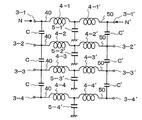
図1は、この発明の第1実施例に係るノイズ対策部品の実装構造を示す斜視図であり、図2は、ノイズ対策部品を配線基板から取り外して示す斜視図であり、図3は、図2のノイズ対策部品を分解して示す斜視図である。 FIG. 1 is a perspective view showing a mounting structure of a noise countermeasure component according to a first embodiment of the present invention, FIG. 2 is a perspective view showing the noise countermeasure component removed from a wiring board, and FIG. It is a perspective view which decomposes | disassembles and shows 2 noise countermeasure components.
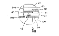
この実施例のノイズ対策部品の実装構造は、図1に示すように、ノイズ対策部品1を配線基板100上に実装する構造である。
すなわち、図2に示すように、ノイズ対策部品1は、4つの入力側外部電極3−1〜3−4を絶縁体2の前面2aに有すると共に、これらの電極と対向する4つの出力側外部電極3−1′〜3−4′を後面2bに有し、グランド用外部電極3−5,3−6を絶縁体2の両側面2c,2cに有している。このようなノイズ対策部品1は、配線基板100上の平面導体10の真上に位置しており、その入力側外部電極3−1〜3−4が入力側の4本の信号配線101〜104に接続される共に、出力側外部電極3−1′〜3−4′が出力側の4本の信号配線101〜104に接続され、グランド用外部電極3−5,3−6がグランド配線111,112に接続される。
The mounting structure of the noise countermeasure component of this embodiment is a structure in which the
That is, as shown in FIG. 2, the
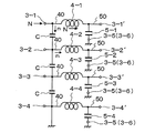
ノイズ対策部品1には、図3に示すように、4つのコイル体4−1〜4−4と4つのコンデンサ5−1〜5−4とが収納されている。
具体的には、絶縁体2が8つの絶縁層21〜28で形成され、各コイル体4−1(4−2〜4−4)の最下位の輪状の導体パターン41が絶縁層21上に形成され、その上の輪状の導体パターン42が絶縁層22上に形成され、最上位の輪状の導体パターン43が絶縁層23上に形成されている。
そして、導体パターン41の先端部41bが、絶縁層22に形成されたビアホール22aを通じて導体パターン42の基端部42aに接続され、この導体パターン42の先端部42bが絶縁層23に形成されたビアホール23aを通じて導体パターン43の基端部43aに接続されている。これにより、全てのコイル体4−1〜4−4が絶縁体2内に螺旋状に形成され、コイル体4−1〜4−4が、上下方向を向いた状態で、絶縁体2内に横並びに収納された状態になっている。
As shown in FIG. 3, the
Specifically, the
The leading
かかる状態においては、導体パターン41の基端部41aが各コイル体4−1(4−2〜4−4)の下端となり、入力側引き出し電極40が、この基端部41aから引き出され、その先端が絶縁体2の前面2a(図2参照)に露出している。
具体的には、各コイル体4−1(4−2〜4−4)の各入力側引き出し電極40は、絶縁体2の下面2dに対して平行に引き出され、前面2aから露出した先端が、各入力側外部電極3−1(3−2〜3−4)に電気的に接続されている。
また、導体パターン43の先端部43bは、絶縁層24に形成されたビアホール24aを通じて後述する電極51に接続されている。そして、出力側引き出し電極50がこの電極51から引き出され、その先端が絶縁体2の後面2b(図2参照)に露出し、この先端が、各出力側外部電極3−1′(3−2′〜3−4′)に電気的に接続されている。
In such a state, the
Specifically, each input-side lead electrode 40 of each coil body 4-1 (4-2 to 4-4) is drawn parallel to the
Further, the
各コンデンサ5−1(5−2〜5−4)は、電極51と、広面積の共通のグランド電極52とを備える。この実施例では、これら電極51とグランド電極52を2組設け、電極51とグランド電極52とを対向させ且つ交互に配することで、各コンデンサ5−1(5−2〜5−4)を構成した。
具体的には、コンデンサ5−1〜5−4の下位の4つの電極51が、絶縁層24上に形成され、1つのグランド電極52が絶縁層25上に形成されている。同様に、上位の4つの電極51が、絶縁層26上に形成され、1つのグランド電極52が絶縁層27上に形成されている。そして、絶縁層25,27上のグランド電極52の両引き出し電極52a,52bが、両側に引き出され、これら引き出し電極52a,52bがグランド用外部電極3−5,3−6に接続されている。
Each capacitor 5-1 (5-2 to 5-4) includes an
Specifically, the lower four
図4は、ノイズ対策部品1の等価回路図である。
図1〜図3に示したように、各コイル体4−1(4−2〜4−4)の出力側引き出し電極50の途中部に各コンデンサ5−1(5−2〜5−4)の一方端である電極51が接続され、他方端であるグランド電極52の両引き出し電極52a,52bがグランド用外部電極3−5,3−6に接続されている。
したがって、各入力側外部電極3−1(3−2〜3−4)と入力側引き出し電極40と各コイル体4−1(4−2〜4−4)と各コンデンサ5−1(5−2〜5−4)と出力側引き出し電極50と各出力側外部電極3−1′(3−2′〜3−4′)との構造は、図4に示すような回路と等価であり、L型フィルタを構成する。すなわち、この実施例のノイズ対策部品1では、4つのL型フィルタが絶縁体2内に構成されている。
FIG. 4 is an equivalent circuit diagram of the
As shown in FIGS. 1 to 3, each capacitor 5-1 (5-2 to 5-4) is provided in the middle of the output-
Therefore, each input side external electrode 3-1 (3-2 to 3-4), the input
図5は、図1の矢視A−A断面図であり、図6は、図1の矢視B−B断面図である。
一方、配線基板100には、図2及び図3に示すように、入力側の4本の信号配線101〜104と、出力側の4本の信号配線101〜104と、グランド配線111,112とが設けられている。そして、ノイズ対策部品1がこれらの配線上に実装される領域、すなわち、実装されるノイズ対策部品1の真下の位置に、1つの平面導体10が設けられている。
5 is a cross-sectional view taken along the line AA in FIG. 1, and FIG. 6 is a cross-sectional view taken along the line BB in FIG.
On the other hand, on the
この平面導体10は、図5に示すように、配線基板100の裏面側に設けられたベタのグランド層120にビアホール121を通じて接続された矩形状の導体パターンであり、その大きさは、全てのコイル体4−1〜4−4を含む大きさに設定されている。また、この平面導体10は、図6に示すように、全てのコイル体4−1〜4−4の入力側引き出し電極40の下側に位置する大きさに設定されている。
As shown in FIG. 5, the
図6に示すように、ノイズ対策部品1の4つの入力側外部電極3−1〜3−4が、入力側の4本の信号配線101〜104に接続される共に、4つの出力側外部電極3−1′〜3−4′が出力側の4本の信号配線101〜104に接続されている。そして、図5に示すように、グランド用外部電極3−5,3−6がグランド配線111,112に接続されることで、ノイズ対策部品1が平面導体10の真上に位置する。これにより、全てのコイル体4−1〜4−4の下端面が平面導体10と対向すると共に、全ての入力側引き出し電極40が平面導体10と対向する。
図7は、図6の破線丸囲み部分の拡大図であり、図8は、この実施例のノイズ対策部品1の実装構造の等価回路図である。
図7に示すように、入力側引き出し電極40が平面導体10と対向することで、容量Cが、入力側引き出し電極40と平面導体10との間に発生する。この結果、ノイズ対策部品1の実装構造は、図8に示す回路と等価となる。
As shown in FIG. 6, the four input side external electrodes 3-1 to 3-4 of the
FIG. 7 is an enlarged view of a portion surrounded by a broken line in FIG. 6, and FIG. 8 is an equivalent circuit diagram of the mounting structure of the
As shown in FIG. 7, the input-
次に、この実施例のノイズ対策部品1の実装構造が示す作用及び効果について説明する。
図9は、この実施例のノイズ対策部品1の実装構造が示す作用及び効果を説明するための等価回路図である。
図1に示す実装状態において、ノイズNが信号配線101から入力側外部電極3−1を通じて入力側引き出し電極40に入力されると、図9の矢印で示すように、ノイズNは、入力側引き出し電極40を通じてコイル体4−1に入力し、このコイル体4−1によって減衰される。そして、コイル体4−1を通過したノイズNは、出力側引き出し電極50の前段に接続されたコンデンサ5−1に入力し、グランド用外部電極3−5,3−6を通じてグランド配線111,112(図2及び図3参照)上に流出する。すなわち、信号配線101からノイズ対策部品1に入力したノイズNは、コイル体4−1とコンデンサ5−1とで構成されるL型フィルタによって減衰される。この結果、入力側の信号配線101からノイズ対策部品1を通過して、出力側の信号配線101に出力されるノイズNは少なく、ノイズ対策部品1によるノイズ透過率は極めて小さくなる。
Next, the operation and effect of the mounting structure of the
FIG. 9 is an equivalent circuit diagram for explaining the operation and effect of the mounting structure of the
In the mounting state shown in FIG. 1, when noise N is input from the
ところで、信号配線101から入力側外部電極3−1に侵入したノイズNのうち、コイル体4−1に入力することができず、入力側引き出し電極40で反射されるようなノイズnが生じる。
しかしながら、この実施例では、上記したように、コイル体4−1〜4−4の入力側引き出し電極40と平面導体10との間に、容量Cが発生し、4つの入力側引き出し電極40同士が、この容量Cによって、接続された状態になっている。このため、コイル体4−1の入力側引き出し電極40によって反射されるノイズnは、容量Cを通じて他のL型フィルタに入力する。すなわち、ノイズnは、コイル体4−2とコンデンサ5−2とで構成されるL型フィルタ、コイル体4−3とコンデンサ5−3とで構成されるL型フィルタ、コイル体4−4とコンデンサ5−4とで構成されるL型フィルタのいずれか又は全てに容量Cを通じて入力し、各L型フィルタにおいて減衰される。
このように、信号配線101から入力側外部電極3−1を通じて入力側引き出し電極40に侵入したノイズは、ほとんど反射されることなく、他のL型フィルタで減衰されるので、ノイズの反射量は非常に少ない。
Of the noise N that has entered the input-side external electrode 3-1 from the
However, in this embodiment, as described above, a capacitance C is generated between the input-
As described above, the noise that has entered the input-
図10は、平面導体10の磁界遮蔽作用を説明するための断面図である。
信号やノイズが、ノイズ対策部品1のコイル体4−1〜4−4に流れると、図10の破線で示すように、磁界Hが、コイル体4−1〜4−4から発生し、この磁界Hが、配線基板100上の信号配線101〜104(図1〜図3参照)や図示しない回路などと磁気結合するおそれがある。
しかし、この実施例では、平面導体10が、上下方向を向く全てのコイル体4−1〜4−4の下端面に対向している。したがって、コイル体4−1〜4−4から下方に向かう磁界Hは、平面導体10によってほぼ完全に遮蔽される。
FIG. 10 is a cross-sectional view for explaining the magnetic field shielding action of the
When a signal or noise flows through the coil bodies 4-1 to 4-4 of the
However, in this embodiment, the
以上のように、この実施例のノイズ対策部品1の実装構造によれば、ノイズの反射量を低減させることができるので、ノイズ透過率を小さくすることができるだけなく、ノイズ反射率をも小さくすることができ、この結果、ノイズ除去効果の向上を図ることができる。
さらに、コイル体4−1〜4−4から放出される磁界Hを平面導体10によって遮蔽して、配線基板100上の信号配線101〜104等への磁気結合を防ぐことができる。
As described above, according to the mounting structure of the
Furthermore, the magnetic field H emitted from the coil bodies 4-1 to 4-4 can be shielded by the
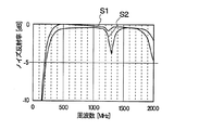
発明者は、ノイズ反射率の減少効果を確認すべく、次のようなシミュレーションを行った。
図11は、ノイズ透過率のシミュレーション結果を示す線図であり、図12は、ノイズ反射率のシミュレーション結果を示す線図である。
まず、図2に示した配線基板100に平面導体10を設けずに、ノイズ対策部品1をこの配線基板100に実装し、ノイズを、このノイズ対策部品1に30MHz〜2GHzの範囲で入力し、このノイズの透過率を計算したところ、図11の曲線S1のような結果を得た。
次に、平面導体10を配線基板100に設けて、ノイズ対策部品1をこの配線基板100に実装し、ノイズを、このノイズ対策部品1に30MHz〜2GHzの範囲で入力し、このノイズの透過率を計算したところ、図11の曲線S2のような結果を得た。
この結果から、発明者は、平面導体10を設けた実装構造におけるノイズ透過率の方が、平面導体10を設けない実装構造におけるノイズ透過率に比べて、小さくなることを確認した。
The inventor conducted the following simulation in order to confirm the effect of reducing the noise reflectance.
FIG. 11 is a diagram showing a simulation result of noise transmittance, and FIG. 12 is a diagram showing a simulation result of noise reflectance.
First, the
Next, the
From this result, the inventor confirmed that the noise transmittance in the mounting structure provided with the
そして、同様の条件下で、平面導体10を設けない実装構造におけるノイズ反射率を計算したところ、図12の曲線S1のような結果を得、平面導体10を設けた実装構造におけるノイズ反射率を計算したところ、図12の曲線S2のような結果を得た。
この結果から、発明者は、平面導体10を設けた実装構造におけるノイズ反射率の方が、平面導体10を設けない実装構造におけるノイズ反射率に比べて、かなり小さくなることを確認した。
Then, under the same conditions, the noise reflectance in the mounting structure without the
From this result, the inventor confirmed that the noise reflectance in the mounting structure provided with the
次に、この発明の第2実施例について説明する。
図13は、この発明の第2実施例に係るノイズ対策部品1の実装構造を示す図5に対応した断面図であり、図14は、図6に対応した断面図である。
上記第1実施例では、図5及び図6に示したように、平面導体10を、配線基板100の裏面側に設けられたグランド層120にビアホール121を通じて接続して、接地状態にしたが、この実施例では、図13及び図14に示すように、平面導体10を、グランド層120に接続せず、非接地状態にした。
Next explained is the second embodiment of the invention.
13 is a cross-sectional view corresponding to FIG. 5 showing the mounting structure of the
In the first embodiment, as shown in FIGS. 5 and 6, the
このように、平面導体10を、非接地状態にすることで、各入力側引き出し電極40と平面導体10との間に生じる容量Cを大きくすることができる。これにより、ノイズ透過率やノイズ反射率をさらに小さくすることができる。
Thus, the capacitance C generated between each input-
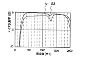
発明者は、第2実施例におけるノイズ反射率の減少効果を確認すべく、次のようなシミュレーションを行った。
図15は、ノイズ透過率のシミュレーション結果を示す線図であり、図16は、ノイズ反射率のシミュレーション結果を示す線図である。
まず、ノイズを、平面導体10を設けない配線基板100に実装したノイズ対策部品1に30MHz〜2GHzの範囲で入力し、このノイズの透過率を計算したところ、図15の曲線S1のような結果を得た。
次に、ノイズ対策部品1を、平面導体10を設け且つ平面導体10を非接地状態にした配線基板100に実装し、ノイズを、このノイズ対策部品1に30MHz〜2GHzの範囲で入力して、このノイズの透過率を計算したところ、図15の曲線S3のような結果を得た。
この結果から、発明者は、平面導体10を設け且つ平面導体10を非接地状態にした実装構造におけるノイズ透過率の方が、平面導体10を設けない実装構造におけるノイズ透過率に比べて、遙かに小さくなることを確認した。さらに、図11の曲線S2と比較したところ、平面導体10を設け且つ平面導体10を非接地状態にした実装構造におけるノイズ透過率の方が、平面導体10を設け且つ平面導体10を接地状態にした実装構造におけるノイズ透過率よりも小さくなることが確認された。
The inventor performed the following simulation in order to confirm the effect of reducing the noise reflectance in the second embodiment.
FIG. 15 is a diagram showing a simulation result of noise transmittance, and FIG. 16 is a diagram showing a simulation result of noise reflectance.
First, noise is input to the
Next, the
From this result, the inventor found that the noise transmittance in the mounting structure in which the
そして、同様の条件下で、平面導体10を設けない実装構造におけるノイズ反射率を計算したところ、図16の曲線S1のような結果を得、平面導体10を設け且つ平面導体10を非接地状態にした実装構造におけるノイズ反射率を計算したところ、図16の曲線S3のような結果を得た。
この結果から、発明者は、平面導体10を設け且つ平面導体10を非接地状態にした実装構造におけるノイズ反射率の方が、平面導体10を設けない実装構造におけるノイズ反射率に比べて、遙かに小さくなることを確認した。さらに、図12の曲線S2と比較したところ、平面導体10を設け且つ平面導体10を非接地状態にした実装構造におけるノイズ反射率の方が、平面導体10を設け且つ平面導体10を接地状態にした実装構造におけるノイズ反射率よりも小さくなることが確認された。
その他の構成、作用及び効果は、上記第1実施例と同様であるので、その記載は省略する。
And when the noise reflectance in the mounting structure where the
From this result, the inventor found that the noise reflectance in the mounting structure in which the
Since other configurations, operations, and effects are the same as those in the first embodiment, description thereof is omitted.
次に、この発明の第3実施例について説明する。
図17は、この発明の第3実施例に係るノイズ対策部品の実装構造の要部であるノイズ対策部品を分解して示す斜視図である。
この実施例は、ノイズ対策部品内に4つのT型フィルタを構成した点が、上記第1実施例と異なる。
図17に示すように、ノイズ対策部品1′は、コイル体4−1〜4−4と、コイル体4−1〜4−4とは別体のコイル体4−1′〜4−4′と、4つのコンデンサ5−1′〜5−4′とを備えている。
各コイル体4−1′(4−2′〜4−4′)は、各コイル体4−1(4−2〜4−4)と同構造であり、各コイル体4−1(4−2〜4−4)を中心軸に関して180°回転した構造を成す。
具体的には、各コイル体4−1′(4−2′〜4−4′)の最下位の導体パターン41′が絶縁層21上に形成され、その上の導体パターン42′が絶縁層22上に形成され、最上位の導体パターン43′が絶縁層23上に形成されている。
そして、導体パターン41′の先端部41b′が、絶縁層22に形成されたビアホールを通じて導体パターン42′の基端部42a′に接続され、この導体パターン42′の先端部42b′が絶縁層23に形成されたビアホールを通じて導体パターン43′の基端部43a′に接続されている。これにより、螺旋状の各コイル体4−1′(4−2′〜4−4′)が、各コイル体4−1(4−2〜4−4)の隣に並んだ状態になっている。
Next explained is the third embodiment of the invention.
FIG. 17 is an exploded perspective view showing a noise countermeasure component which is a main part of the mounting structure of the noise countermeasure component according to the third embodiment of the present invention.
This embodiment is different from the first embodiment in that four T-type filters are configured in the noise countermeasure component.
As shown in FIG. 17, the
Each coil body 4-1 ′ (4-2 ′ to 4-4 ′) has the same structure as each coil body 4-1 (4-2 to 4-4), and each coil body 4-1 (4- 2-4-4) is rotated 180 ° with respect to the central axis.
Specifically, the lowermost conductor pattern 41 'of each coil body 4-1' (4-2 'to 4-4') is formed on the insulating
The
かかる状態においては、導体パターン41′の基端部41a′が各コイル体4−1′(4−2′〜4−4′)の下端となり、出力側引き出し電極50が、この基端部41a′から引き出され、その先端が絶縁体2の後面2bに露出している。
具体的には、各コイル体4−1′(4−2′〜4−4′)の各出力側引き出し電極50は、絶縁体2の下面2dに対して平行に引き出され、後面2bから露出した先端が、各出力側外部電極3−1′(3−2′〜3−4′)に電気的に接続されている。
また、導体パターン43′の先端部43b′は、絶縁層24に形成されたビアホールを通じて後述する電極51′に接続されている。そして、各コイル体4−1(4−2〜4−4)の導体パターン43の先端部43bも当該電極51′に接続されている。すなわち、各コイル体4−1′(4−2′〜4−4′)の入力側端部である先端部43b′が、電極51を通じて、各コイル体4−1(4−2〜4−4)の出力側端部である先端部43bに接続された状態になっている。
In such a state, the
Specifically, each output-
Further, the
各コンデンサ5−1′(5−2′〜5−4′)は、電極51′と、広面積の共通のグランド電極52′とを備える。
具体的には、コンデンサ5−1′〜5−4′の4つの電極51′が、絶縁層24上に形成され、1つのグランド電極52′が絶縁層25上に形成されている。そして、グランド電極52′の両引き出し電極52a′,52b′が、両側に引き出され、これら引き出し電極52a′,52b′がグランド用外部電極3−5,3−6に接続されている。
Each capacitor 5-1 ′ (5-2 ′ to 5-4 ′) includes an
Specifically, four
図18は、この実施例のノイズ対策部品1′の実装構造の等価回路図である。
図17に示したように、各コンデンサ5−1′(5−2′〜5−4′)の一方端である電極51′が、各コイル体4−1(4−2〜4−4)と各コイル体4−1′(4−2′〜4−4′)との接続部に接続され、他方端であるグランド電極52の両引き出し電極52a,52bがグランド用外部電極3−5,3−6に接続されている。
したがって、各入力側外部電極3−1(3−2〜3−4)と入力側引き出し電極40と各コイル体4−1(4−2〜4−4)と各コンデンサ5−1(5−2〜5−4)と各コイル体4−1′(4−2′〜4−4′)と出力側引き出し電極50と各出力側外部電極3−1′(3−2′〜3−4′)との構造は、図18に示すような回路と等価であり、T型フィルタを構成する。すなわち、この実施例のノイズ対策部品1′では、4つのT型フィルタが絶縁体2内に構成されている。
FIG. 18 is an equivalent circuit diagram of the mounting structure of the
As shown in FIG. 17, the electrode 51 'which is one end of each capacitor 5-1' (5-2 'to 5-4') is connected to each coil body 4-1 (4-2 to 4-4). Are connected to the connecting portions of the coil bodies 4-1 ′ (4-2 ′ to 4-4 ′), and the
Therefore, each input side external electrode 3-1 (3-2 to 3-4), the input
かかる構造のノイズ対策部品1′も、図17に示すように、配線基板100上の信号配線101〜104とグランド配線111,112上に実装され、平面導体10′がノイズ対策部品1′の真下に位置することとなる。
平面導体10′の大きさは、コイル体4−1′〜4−4′が設けられている領域の分だけ、第1実施例の平面導体10よりも大きく設定されている。これにより、平面導体10′が、コイル体4−1〜4−4の下面だけでなく、コイル体4−1′〜4−4′の下面にも対向し、また、コイル体4−1〜4−4の入力側引き出し電極40だけでなく、コイル体4−1′〜4−4′の出力側引き出し電極50にも対向する。これにより、平面導体10′と出力側引き出し電極50との間にも容量C′が生成される。
As shown in FIG. 17, the
The size of the planar conductor 10 'is set larger than that of the
かかる構成により、図18に示すように、各コイル体4−1(4−2〜4−4)の入力側引き出し電極40側から入力したノイズNの反射量を低減させることができるだけでなく、各コイル体4−1′(4−2′〜4−4′)の出力側引き出し電極50側から入力したノイズN′の反射量も低減させることができる。
その他の構成、作用及び効果は、上記第1及び第2実施例と同様であるので、その記載は省略する。
With this configuration, as shown in FIG. 18, not only can the amount of reflection of noise N input from the input-
Other configurations, operations, and effects are the same as those in the first and second embodiments, and thus description thereof is omitted.
なお、この発明は、上記実施例に限定されるものではなく、発明の要旨の範囲内において種々の変形や変更が可能である。
例えば、上記第1〜第3実施例においては、コンデンサ5−1〜5−4,5−1′〜5−4′を設けたフィルタとしてのノイズ対策部品について説明したが、コンデンサ5−1〜5−4,5−1′〜5−4′を備えず、コイル体だけで構成されたノイズ対策部品の実装構造もこの発明の範囲に含まれることは勿論である。
In addition, this invention is not limited to the said Example, A various deformation | transformation and change are possible within the range of the summary of invention.
For example, in the first to third embodiments, the noise countermeasure component as the filter provided with the capacitors 5-1 to 5-4, 5-1 'to 5-4' has been described. Needless to say, a mounting structure of a noise countermeasure component which is not provided with 5-4, 5-1 'to 5-4' but is constituted only by a coil body is also included in the scope of the present invention.
1,1′…ノイズ対策部品、 2…絶縁体、 2a…前面、 2b…後面、 2c…側面、 2d…下面、 3−5,3−6…グランド用外部電極、 3−1〜3−4…入力側外部電極、 3−1′〜3−4′…出力側外部電極、 4−1〜4−4,4−1′〜4−4′…コイル体、 5−1〜5−4,5−1′〜5−4′…コンデンサ、 10,10′…平面導体、 21〜28…絶縁層、 22a〜24a…ビアホール、 40…入力側引き出し電極40、 41〜43,41′〜43′…導体パターン、 41a〜43a,41a′〜43a′…基端部、 41b〜43b,41b′〜43b′…先端部、 50…出力側引き出し電極、 51…電極、 52…グランド電極、 52a,52b,52a′,52b′…引き出し電極、 101〜104…信号配線、 111,112…グランド配線、 120…グランド層、 121…ビアホール、 C,C′…容量。
DESCRIPTION OF
Claims (5)
上記各コイル体の各入力側引き出し電極を、絶縁体の下面に対して平行に引き出し、
上記ノイズ対策部品が実装される配線基板上の領域に、1つの平面導体を上記n数の入力側引き出し電極と対向するように配設した、
ことを特徴とするノイズ対策部品の実装構造。 Insulator and n number (n is an integer of 2 or more) stored side by side in this insulator with the input lead electrode at the lower end exposed on the front face of the insulator and the output lead electrode exposed on the rear face A coil body, n number of input side external electrodes provided on the front surface of the insulator and electrically connected to the n number of input side lead electrodes, respectively, and n number of the above described external electrodes provided on the rear surface of the insulator. A noise countermeasure component mounting structure for mounting a noise countermeasure component having n number of output side external electrodes electrically connected to the output side lead electrode on the signal wiring of the wiring board,
Each input-side extraction electrode of each coil body is extracted in parallel to the lower surface of the insulator,
In the region on the wiring board on which the noise countermeasure component is mounted, one planar conductor is disposed so as to face the n number of input side extraction electrodes.
A mounting structure for noise suppression components.
上記全てのコイル体を、上記絶縁体の上下方向に向けて絶縁体内に収納すると共に、
上記配線基板上の平面導体の大きさを、当該平面導体が上記全てのコイル体の下端面と対向する大きさに設定した、
ことを特徴とするノイズ対策部品の実装構造。 In the mounting structure of the noise countermeasure component according to claim 1,
While storing all the coil bodies in the insulator in the vertical direction of the insulator,
The size of the planar conductor on the wiring board was set to a size where the planar conductor faces the lower end surfaces of all the coil bodies,
A mounting structure for noise suppression components.
上記平面導体を、非接地状態にした、
ことを特徴とするノイズ対策部品の実装構造。 In the mounting structure of the noise countermeasure component according to claim 1 or 2,
The planar conductor was ungrounded,
A mounting structure for noise suppression components.
上記各コイル体の出力側引き出し電極の途中部に一方端が接続され且つ他方端が絶縁体の側面に露出したコンデンサを上記絶縁体内に設けると共に、当該コンデンサの他方端に電気的に接続するグランド用外部電極を絶縁体の上記側面に設けることで、
上記ノイズ対策部品内にn数のL型フィルタを構成し、
上記グランド用外部電極を上記配線基板上に設けたグランド配線に接続した、
ことを特徴とするノイズ対策部品の実装構造。 In the mounting structure of the noise countermeasure component according to any one of claims 1 to 3,
A capacitor having one end connected to the middle portion of the output-side lead electrode of each coil body and the other end exposed on the side surface of the insulator is provided in the insulator and is electrically connected to the other end of the capacitor. By providing external electrodes for the above side surfaces of the insulator,
N number of L-type filters are configured in the noise suppression component,
The ground external electrode was connected to a ground wiring provided on the wiring board.
A mounting structure for noise suppression components.
上記各コイル体の出力側端部に各入力側端部が接続され且つ各出力側引き出し電極が上記絶縁体の後面に露出された別体のコイル体を絶縁体内に設け、当該各出力側引き出し電極を、絶縁体の下面に対して平行に引き出して、上記出力側外部電極をこの出力側引き出し電極に電気的に接続し、且つ上記コイル体と別体のコイル体との接続部に一方端が接続され且つ他方端が絶縁体の側面に露出したコンデンサを上記絶縁体内に設けると共に、当該コンデンサの他方端に電気的に接続するグランド用外部電極を絶縁体の上記側面に設けることで、上記ノイズ対策部品内にn数のT型フィルタを構成し、
上記グランド用外部電極を上記配線基板上に設けたグランド配線に接続すると共に、上記配線基板上の平面導体の大きさを、当該平面導体が上記別体のコイル体の出力側引き出し電極にも対向するような大きさに設定した、
ことを特徴とするノイズ対策部品の実装構造。 In the mounting structure of the noise countermeasure component according to any one of claims 1 to 3,
A separate coil body, in which each input side end is connected to the output side end of each coil body and each output side lead electrode is exposed on the rear surface of the insulator, is provided in the insulator, and each output side lead is provided. An electrode is pulled out parallel to the lower surface of the insulator, the output-side external electrode is electrically connected to the output-side lead electrode, and one end is connected to a connection portion between the coil body and a separate coil body. Is provided in the insulator, and a ground external electrode that is electrically connected to the other end of the capacitor is provided on the side surface of the insulator. Configure n number of T-type filters in the noise countermeasure component,
The ground external electrode is connected to the ground wiring provided on the wiring board, and the size of the planar conductor on the wiring board is set so that the planar conductor faces the output-side extraction electrode of the separate coil body. Set the size to
A mounting structure for noise suppression components.
Priority Applications (1)
| Application Number | Priority Date | Filing Date | Title |
|---|---|---|---|
| JP2008228258A JP2010062986A (en) | 2008-09-05 | 2008-09-05 | Mounting structure for noise-proof component |
Applications Claiming Priority (1)
| Application Number | Priority Date | Filing Date | Title |
|---|---|---|---|
| JP2008228258A JP2010062986A (en) | 2008-09-05 | 2008-09-05 | Mounting structure for noise-proof component |
Publications (1)
| Publication Number | Publication Date |
|---|---|
| JP2010062986A true JP2010062986A (en) | 2010-03-18 |
Family
ID=42189275
Family Applications (1)
| Application Number | Title | Priority Date | Filing Date |
|---|---|---|---|
| JP2008228258A Pending JP2010062986A (en) | 2008-09-05 | 2008-09-05 | Mounting structure for noise-proof component |
Country Status (1)
| Country | Link |
|---|---|
| JP (1) | JP2010062986A (en) |
Cited By (3)
| Publication number | Priority date | Publication date | Assignee | Title |
|---|---|---|---|---|
| CN105225806A (en) * | 2014-06-26 | 2016-01-06 | 株式会社村田制作所 | Coil module |
| CN105723598A (en) * | 2013-10-17 | 2016-06-29 | 三菱电机株式会社 | Noise filter |
| WO2017010265A1 (en) * | 2015-07-10 | 2017-01-19 | 株式会社村田製作所 | Surface mounted filter and surface mounted filter array |
-
2008
- 2008-09-05 JP JP2008228258A patent/JP2010062986A/en active Pending
Cited By (6)
| Publication number | Priority date | Publication date | Assignee | Title |
|---|---|---|---|---|
| CN105723598A (en) * | 2013-10-17 | 2016-06-29 | 三菱电机株式会社 | Noise filter |
| EP3059838A4 (en) * | 2013-10-17 | 2017-07-05 | Mitsubishi Electric Corporation | Noise filter |
| US10063209B2 (en) | 2013-10-17 | 2018-08-28 | Mitsubishi Electric Corporation | Noise filter |
| CN105225806A (en) * | 2014-06-26 | 2016-01-06 | 株式会社村田制作所 | Coil module |
| WO2017010265A1 (en) * | 2015-07-10 | 2017-01-19 | 株式会社村田製作所 | Surface mounted filter and surface mounted filter array |
| JPWO2017010265A1 (en) * | 2015-07-10 | 2018-02-15 | 株式会社村田製作所 | Surface mount filter array |
Similar Documents
| Publication | Publication Date | Title |
|---|---|---|
| JP4925185B2 (en) | Noise filter array | |
| JP6791107B2 (en) | Stacked band pass filter | |
| TWI656543B (en) | Electronic parts | |
| WO2018168653A1 (en) | High frequency module | |
| US7859364B2 (en) | Layered low-pass filter | |
| US20090033439A1 (en) | Multilayer filter | |
| US9325049B2 (en) | Transmission line and filtering module thereof | |
| JP2004014961A (en) | Laminated through-type capacitor | |
| US9083313B2 (en) | Substrate, duplexer and substrate module | |
| KR100702751B1 (en) | Ultra-high-frequency notch filter | |
| JP4627791B2 (en) | Balance-unbalance conversion circuit | |
| CN108432133A (en) | High-frequency model | |
| JP2010062986A (en) | Mounting structure for noise-proof component | |
| JP6411288B2 (en) | Ladder filters, duplexers and modules | |
| JP2011077581A (en) | Common mode choke coil mounting structure, and common mode choke coil mounting method | |
| JP3201005B2 (en) | Duplexer | |
| KR102424038B1 (en) | multiplexer | |
| CN101005731A (en) | EMI supppression method for audio frequency signal | |
| JP2008167157A (en) | High-pass filter | |
| US7782157B2 (en) | Resonant circuit, filter circuit, and multilayered substrate | |
| JP5007499B2 (en) | Noise filter array | |
| JPWO2016072403A1 (en) | Flexible cable connection structure to printed circuit board | |
| JP4505440B2 (en) | Multilayer high-pass filter | |
| JP6489859B2 (en) | Filter device | |
| JP2023125379A (en) | Laminated electronic component |