JP2010009208A - Interface device and mobile terminal apparatus - Google Patents
Interface device and mobile terminal apparatus Download PDFInfo
- Publication number
- JP2010009208A JP2010009208A JP2008165967A JP2008165967A JP2010009208A JP 2010009208 A JP2010009208 A JP 2010009208A JP 2008165967 A JP2008165967 A JP 2008165967A JP 2008165967 A JP2008165967 A JP 2008165967A JP 2010009208 A JP2010009208 A JP 2010009208A
- Authority
- JP
- Japan
- Prior art keywords
- external
- circuit
- power
- input
- terminal
- Prior art date
- Legal status (The legal status is an assumption and is not a legal conclusion. Google has not performed a legal analysis and makes no representation as to the accuracy of the status listed.)
- Granted
Links
Images

Landscapes
- Power Sources (AREA)
Abstract
Description
本発明は、外部第1信号ライン(VBUS端子)と外部第2信号ライン(ID端子)に3種類の外部機器のいずれか1つが接続されることにより、それぞれの外部機器に応じて本体側をホスト機器またはスレーブ機器のいずれかの機能に切り換え制御するインタフェース装置に関する。 In the present invention, any one of the three types of external devices is connected to the external first signal line (VBUS terminal) and the external second signal line (ID terminal), so that the main body side is set according to each external device. The present invention relates to an interface device that performs switching control to a function of either a host device or a slave device.
従来、USBインタフェースは、接続機器に対して給電する機器(ホスト機器)となることが可能であり、また逆に、接続機器から受電する機器(スレーブ機器)となることが可能なインタフェース回路である。 Conventionally, a USB interface is an interface circuit that can be a device (host device) that supplies power to a connected device, and conversely, can be a device (slave device) that receives power from the connected device. .
このようなUSBインタフェースを電池駆動で屋外でも使用され得る機器(携帯端末機器)に搭載した場合、接続機器のタイプに応じて、給電可能状態とするか受電可能状態とするかを判断し制御する必要があった。 When such a USB interface is mounted on a battery-powered device (portable terminal device) that can be used outdoors, it is determined and controlled according to the type of connected device, whether it is in a power-feedable state or a power-receivable state. There was a need.
そこで、異種タイプの機器を同一端子(1つの端子)で接続可能としたシステムとして、受電デバイス(例えば、マウス等)と規格内給電機器(例えば、パーソナルコンピュータ(PC)等)との切り換え接続が可能なシステム(これを、従来技術1という。)、及び、規格内給電機器(例えばパーソナルコンピュータ(PC))と規格外給電機器(例えば、ACアダプタ)との切り換え接続が可能なシステム(これを、従来技術2という。)の2つのシステムが提案されている。 Therefore, as a system in which different types of devices can be connected with the same terminal (one terminal), switching connection between a power receiving device (for example, a mouse) and a standard-standard power supply device (for example, a personal computer (PC)) is possible. Possible systems (this is referred to as Conventional Technology 1), and systems capable of switching connection between non-standard power supply devices (for example, personal computers (PCs)) and non-standard power supply devices (for example, AC adapters). And two systems of prior art 2) have been proposed.
従来技術1のシステムは、ID端子の電圧レベルが「H」から「L」に変換することで、内蔵する電源を接続機器(例えば、マウス等)に給電し、電圧検出回路の出力であるVBUS−DETの値が「L」から「H」に変化することで、接続機器(例えば、PC)と通信後に規格内の電源を接続機器から受電するようになっている。
In the system of
また、従来技術2のシステムは、電圧検出回路の出力であるVBUS−DETの値が「L」から「H」に変化したとき、ID端子の値が「L」である場合には規格外の電源を接続機器(例えば、ACアダプタ)から受電し、ID端子の値が「H」である場合には接続機器(例えば、PC)と通信後に規格内の電源を接続機器から受電するようになっている。
Further, the system of the
上記従来技術1に関連するものとして、特許文献1には、ホストとデバイスがUSBケーブルを介して接続されると、デバイス側のID端子がGNDラインにショートされて該ID端子の電圧レベルが低下し、電力供給手段は、このID端子の電圧レベルが「H」から「L」になったことを感知すると、VBUS端子に電力の供給を開始し、USBケーブルのVBUSラインを介してホストに電力を供給するUSBインタフェースシステムが記載されている。すなわち、特許文献1に記載のUSBインタフェースシステムは、デジタルカメラとプリンタ等、周辺機器同士が、PCを介さずに、USB−OTG制御シーケンスに対応させることなく、電力の送受が可能となるように(すなわち、デバイスであっても、給電するホストとして機能を持たせるために)、ID端子の電圧が所定のレベルまで低下した場合にVBUS端子に電力を供給するようになっている。
As related to the above
一方、特許文献2には、電子機器がスレーブで通常動作モードの時は、USBのVBUS、蓄電池または外部電源からの電源をデータ転送制御回路に供給し、電子機器がスレーブで充電モードの時は、VBUSからの電源を蓄電池に供給して充電する。また、充電モード時に外部電源が使用可能な時は、VBUSに代えて外部電源からの電源を蓄電池に供給する。一方、電子機器がマスターで通常動作モードの時は、蓄電池または外部電源からの電源をデータ転送制御回路、電子機器に供給し、電子機器がマスターで充電モードの時は、電子機器の蓄電池を充電するために蓄電池または外部電源からの電源をVBUSを介して電子機器に供給する電源制御回路が記載されている。すなわち、特許文献2に記載の電源制御回路は、USBのデータ転送におけるスレーブ側で、かつ、通常動作モードに設定された場合には、内蔵電源等を接続機器に給電するように、また、USBのデータ転送におけるスレーブ側で、かつ、充電モードに設定された場合には、接続機器から供給される電源を蓄電池に供給(接続機器から受電)するように制御する構成となっている。
上記従来技術1のように、同一端子で、受電デバイス(例えば、マウス等)と規格内給電機器(例えば、PC等)との切り換え接続を可能としたシステム,及び特許文献1のように、同一端子で周辺機器同士の切り換え接続を可能としたシステムでは、電池駆動での利用が前提となる携帯端末の場合、内蔵電池を充電するために、充電器とドッキングさせるための専用インタフェース、若しくはACアダプタを接続するための専用インタフェースが別途必要となるといった問題があった。
A system that enables switching connection between a power receiving device (for example, a mouse) and an intra-standard power supply device (for example, a PC) with the same terminal as in the
なお、特許文献2に示される電源制御回路では、PC等のUSBホスト機器(規格内給電機器)経由での充電が可能となる。しかし、充電を主体とするシーン(例えば、自宅での就寝時間中の日頃の充電等)では、端末のモード(「通常動作モード」、「充電モード」)に応じて、充電可能状態とするか否かを判断する必要がある。そのため、例えば端末電源のON/OFF状態や、電池残量が所定以上か否かに連動して、上記モードを切り換えるシステムとした場合、充電機能が動作している端末状態かどうかを常に利用者が意識する必要があり、充電機能を利用するために利用者に負荷を与えてしまうといった問題があった。また、USB規格内の電源での充電しかできないため、所定の容量を充電するまでに時間を要する等、あまり有効に機能しない充電システム(充電方法)となっている。
Note that the power supply control circuit disclosed in
一方、上記従来技術2のように、同一端子で、規格内給電機器(例えば、PC)と規格外給電機器(例えば、ACアダプタ)との切り換え接続を可能としたシステムでは、ノートPCにカテゴライズされる比較的大きな携帯端末を除き、一般的に、端末としてマウスや拡張キーボードといった情報機器の入力デバイスの接続をサポートしていない。これは、端末として、情報機器機能よりも優先されるデバイス(例えば、カメラ等)やインタフェース(例えば、音楽/TV音声/ゲーム音声を聴くためのイヤホン等)を、内蔵・配置しているため、拡張用の入力デバイスのインタフェースを別途内蔵・配置することが、非常に困難な状況となっていることに起因している。
On the other hand, as in the above-described
その一方で、携帯電話や携帯ゲーム機等の小型の携帯端末においては、メール送受信やインターネット情報の検索・閲覧機能等を有する情報機器(PC)としての機能がサポートされる等、多機能化が進んでいる。そして、この多機能化に伴い、これら情報機器機能を利用する上において、端末本体に内蔵・配置されているキーやボタンでは、小さくて非常に操作しにくいという相反する課題(すなわち、マウスやPCキーボードの接続が可能な端末のユーザ要求)が存在する。 On the other hand, in small portable terminals such as mobile phones and portable game machines, functions such as information transmission (PC) having functions such as mail transmission / reception and Internet information search / browsing functions are supported. Progressing. And with this multi-functionality, there is a conflicting problem that the keys and buttons built in and arranged in the terminal body are small and very difficult to operate when using these information device functions (ie, mouse and PC). There is a user request for a terminal to which a keyboard can be connected.
本発明はかかる問題点を解決すべく創案されたもので、その目的は、小型化設計が容易となるよう、マウス(受電デバイス)、ACアダプタ(規格外給電機器)、PC(規格内給電機器)の3タイプの機器・デバイスが同一端子で接続可能なインタフェース装置及びこれを搭載した携帯端末機器を提供することにある。 The present invention was devised to solve such problems. The purpose of the present invention is to provide a mouse (power receiving device), an AC adapter (non-standard power supply device), and a PC (in-standard power supply device) so as to facilitate the miniaturization design. 3) devices and devices that can be connected to the same terminal, and a portable terminal device equipped with the interface device.
上記課題を解決するため、本発明のインタフェース装置は、外部第1信号ラインと外部第2信号ラインに3種類の外部機器のいずれか1つが接続されることにより、それぞれの外部機器に応じて本体側をホスト機器またはスレーブ機器のいずれかの機能に切り換え制御するインタフェース装置において、前記外部第1信号ライン及び前記外部第2信号ラインは前記外部機器の未接続時にそれぞれ所定値に設定されており、前記外部第1信号ラインからの信号が入力される電圧検出回路と、前記外部第2信号ラインからの信号が入力されるID端子検出回路と、前記電源検出回路の出力信号と前記ID端子検出回路の出力信号とに基づいて、前記外部第1信号ラインの電源入力または電源出力を切り換え制御する入出力切換制御回路とを備え、前記外部機器の接続時、前記外部第1信号ラインが所定値であり、前記外部第2信号ラインが所定値から遷移した場合、前記入出力切換制御回路は、本体側がホスト機器となるように当該本体側の電源出力回路をオンに切り換え制御し、前記外部第1信号ライン及び前記外部第2信号ラインが共に所定値から遷移した場合、前記入出力切換制御回路は、本体側がスレーブ機器となるように当該本体側の電源入力回路をオンとし、かつ、規格電流値を超えて外部機器から受電可能に切り換え制御し、前記外部第1信号ラインが所定値から遷移し、前記外部第2信号ラインが所定値である場合、前記入出力切換回路は、本体側がスレーブ機器となるように当該本体側の電源入力回路をオンとし、かつ、規格電流値の範囲内で外部機器から受電可能に切り換え制御することを特徴としている。 In order to solve the above-described problems, the interface device according to the present invention has a main body corresponding to each external device by connecting any one of three types of external devices to the external first signal line and the external second signal line. In the interface device for switching and controlling the function to either the host device or the slave device, the external first signal line and the external second signal line are respectively set to predetermined values when the external device is not connected, A voltage detection circuit to which a signal from the external first signal line is input, an ID terminal detection circuit to which a signal from the external second signal line is input, an output signal of the power supply detection circuit, and the ID terminal detection circuit And an input / output switching control circuit for switching and controlling the power input or power output of the external first signal line based on the output signal of When the external device is connected, when the external first signal line is a predetermined value and the external second signal line is transitioned from the predetermined value, the input / output switching control circuit is configured so that the main body side becomes the host device. When the external first signal line and the external second signal line both change from a predetermined value, the input / output switching control circuit is configured so that the main body side becomes a slave device. The power input circuit on the main body side is turned on, and switching control is performed so that power can be received from an external device exceeding a standard current value, the external first signal line is changed from a predetermined value, and the external second signal line is predetermined. If the value is a value, the input / output switching circuit turns on the power input circuit on the main unit so that the main unit becomes a slave device, and switches off power from an external device within the range of the standard current value. It is characterized by switching control.
ここで、3種類の外部機器は、受電デバイス、規格外給電機器、規格内給電機器であり、具体的には、受電デバイスがマウス、規格外給電機器がACアダプタ、規格内給電機器がパーソナルコンピュータである。 Here, the three types of external devices are a power receiving device, a nonstandard power supply device, and a standard power supply device. Specifically, the power receiving device is a mouse, a nonstandard power supply device is an AC adapter, and a standard power supply device is a personal computer. It is.
また、外部第1信号ラインはVBUS端子が接続されているラインであり、外部第2信号ラインはID端子が接続されているラインである。そして、外部第1信号ライン(VBUS端子)は、外部機器の未接続時に所定値として「L」に設定されており、外部第2信号ライン(ID端子)は、外部機器の未接続時に所定値として「H」に設定されている。 The external first signal line is a line to which the VBUS terminal is connected, and the external second signal line is a line to which the ID terminal is connected. The external first signal line (VBUS terminal) is set to “L” as a predetermined value when the external device is not connected, and the external second signal line (ID terminal) is set to a predetermined value when the external device is not connected. Is set to “H”.
なお、本発明のインタフェース装置は、この他にも、外部機器との間でデータの送受信を行うためのデータ端子(D+端子,D−端子)を備えている。 In addition, the interface device of the present invention further includes data terminals (D + terminal, D− terminal) for transmitting / receiving data to / from an external device.
本発明をさらに具体的に説明すると、前記入出力切換制御回路は、前記ID端子検出回路の出力信号と前記電源検出回路の出力信号とに基づいて前記電源入力回路と前記電源出力回路の両方を制御するコントローラと、前記ID端子検出回路の出力信号と前記電源検出回路の出力信号とに基づいて前記電源入力回路を制御する入力オン・オフ切換制御回路とから構成されている。 Describing the present invention more specifically, the input / output switching control circuit controls both the power input circuit and the power output circuit based on the output signal of the ID terminal detection circuit and the output signal of the power supply detection circuit. The controller includes a controller for controlling, and an input on / off switching control circuit for controlling the power input circuit based on an output signal of the ID terminal detection circuit and an output signal of the power supply detection circuit.
そして、外部機器として例えば受電デバイスであるマウスが接続されると、外部第1信号ライン(VBUS端子)が所定値(L)のままであり、外部第2信号ライン(ID端子)が所定値から遷移(HからLに変化)するので、この信号状態に基づき、コントローラは、電源出力回路をオンに切り換え制御する。このとき、外部第1信号ライン(VBUS端子)に接続されている電源入力回路はオフ状態のままとする。これにより、電源出力回路から例えば5Vの電圧がVBUS端子を介してマウスに供給され、本発明のインタフェース装置を搭載した携帯端末機器の周辺機器としてマウスを利用することが可能となる。 For example, when a mouse, which is a power receiving device, is connected as an external device, the external first signal line (VBUS terminal) remains at a predetermined value (L), and the external second signal line (ID terminal) starts from the predetermined value. Since the transition (change from H to L) is made, the controller controls the power output circuit to be turned on based on this signal state. At this time, the power input circuit connected to the external first signal line (VBUS terminal) is kept off. As a result, a voltage of, for example, 5V is supplied from the power output circuit to the mouse via the VBUS terminal, and the mouse can be used as a peripheral device of the portable terminal device equipped with the interface device of the present invention.
また、外部機器として例えば規格外給電機器であるACアダプタが接続されると、外部第1信号ライン(VBUS端子)が所定値から遷移(LからHに変化)し、外部第2信号ライン(ID端子)が所定値から遷移(HからLに変化)するので、この信号状態に基づいて、入力オン・オフ切換制御回路は、電源入力回路をオンに切り換え制御するとともに、コントローラは、規格電流値を超えて外部機器から受電可能に切り換え制御する。このとき、外部第1信号ライン(VBUS端子)に接続されている電源出力回路はオフ状態のままとする。これにより、携帯端末機器の電源回路にACアダプタから規格電流値を超える充電電流が供給されることになる。すなわち、この場合は、ACアダプタに対して本発明の携帯端末機器がスレーブ機器となる。 When an AC adapter, which is a nonstandard power supply device, is connected as an external device, the external first signal line (VBUS terminal) changes from a predetermined value (changes from L to H), and the external second signal line (ID Terminal) changes from a predetermined value (changes from H to L). Based on this signal state, the input on / off switching control circuit controls the power input circuit to be turned on, and the controller Control over switching to enable receiving power from external devices. At this time, the power supply output circuit connected to the external first signal line (VBUS terminal) remains off. As a result, a charging current exceeding the standard current value is supplied from the AC adapter to the power supply circuit of the portable terminal device. That is, in this case, the portable terminal device of the present invention is a slave device with respect to the AC adapter.
また、外部機器として例えば規格内給電機器であるPCが接続されると、外部第1信号ライン(VBUS端子)が所定値から遷移(LからHに変化)し、外部第2信号ライン(ID端子)が所定値(H)のままであるので、この信号状態に基づいて、コントローラは、電源入力回路をオンに切り換え制御するとともに、規格電流値の範囲内で外部機器から受電可能に切り換え制御する。このとき、外部第1信号ライン(VBUS端子)に接続されている電源出力回路はオフ状態のままとする。これにより、携帯端末機器の電源回路にPCから規格電流値の範囲内で電流が供給されることになる。すなわち、この場合は、PCに対して本発明の携帯端末機器がスレーブ機器となる。 In addition, when a PC that is an intra-standard power supply device, for example, is connected as an external device, the external first signal line (VBUS terminal) changes from a predetermined value (changes from L to H), and the external second signal line (ID terminal) ) Remains at the predetermined value (H), and based on this signal state, the controller controls the power input circuit to be turned on, and also performs control so that power can be received from an external device within the range of the standard current value. . At this time, the power supply output circuit connected to the external first signal line (VBUS terminal) remains off. As a result, a current is supplied from the PC within the range of the standard current value to the power supply circuit of the portable terminal device. That is, in this case, the portable terminal device of the present invention is a slave device with respect to the PC.
本発明は上記のように構成したので、端子1つで、受電デバイス、規格内給電機器、規格外給電機器の3タイプの機器・デバイスが接続が可能なインタフェース装置を実現することができる。そのため、このインタフェース装置を携帯端末機器に搭載することで、携帯端末機器の小型化が容易となる。 Since the present invention is configured as described above, it is possible to realize an interface apparatus that can connect three types of devices and devices, that is, a power receiving device, an intra-standard power supply device, and a non-standard power supply device, with a single terminal. Therefore, by mounting this interface device on a mobile terminal device, the mobile terminal device can be easily downsized.
以下、本発明の実施の形態について、図面を参照して説明する。 Embodiments of the present invention will be described below with reference to the drawings.
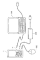
図1は、本実施形態のインタフェース装置を搭載した携帯端末機器に外部機器を接続するイメージ図である。本実施形態の携帯端末機器1は、1つの端子(ここではUSB端子)11に対して、受電デバイスであるマウス100、規格外給電機器であるACアダプタ200、規格内給電機器であるパーソナルコンピュータ(PC)300の3タイプの外部機器のそれぞれが接続可能となっており、これら3タイプの外部機器のいずれか1つがUSB端子11に接続されることにより、それぞれの外部機器に応じて本体側をホスト機器(給電側)またはスレーブ機器(受電側)のいずれかの機能に切り換え制御するインタフェース装置を備えている。
FIG. 1 is an image diagram of connecting an external device to a mobile terminal device equipped with the interface device of the present embodiment. The mobile
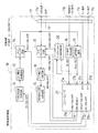
図2は、本実施形態のインタフェース装置を搭載した携帯端末機器の電気的構成を示す機能ブロック図である。ただし、携帯端末機器の機能については、電源系統を除いて全て図示を省略している。 FIG. 2 is a functional block diagram showing an electrical configuration of a portable terminal device equipped with the interface device of the present embodiment. However, all the functions of the mobile terminal device are omitted except for the power supply system.
本実施形態のインタフェース装置10は、外部第1信号ラインであるVBUS端子11aと、外部第2信号ラインであるID端子(判定端子)11bと、接続される外部機器との間でデータの送受信を行うデータ端子(D+端子,D−端子)11cとを備えており、これら端子が1つのUSB端子11としてまとめられている。ここで、外部機器の未接続時、VBUS端子11aは所定値として「L」レベルに設定されている。また、ID端子11bは、図示は省略しているが、プルアップ抵抗を介して3V電源に接続されることにより、所定値として「H」レベルに設定されている。
The
VBUS端子11aには、5V電圧を作成するVBUS電源作成回路12、出力電流制限回路13、出力ON/OFF回路14からなる出力系電源ラインと、携帯端末本体電源回路15、入力電流制限回路16、入力ON/OFF回路17からなる入力系電源ラインとが接続されている。また、VBUS端子11aは、電圧検出回路19の入力端子に接続されており、ID端子11bは、ID端子検出回路18の入力端子に接続されている。
The
また、入力ON/OFF回路17に切換信号(VIN1−ON/OFF)を出力して、該入力ON/OFF回路17をON/OFF制御する入力ON/OFF切換制御回路20には、ID端子検出回路18の出力信号(ID−DET)と電圧検出回路19の出力信号(Vbus−DET)とが導かれている。
The input ON / OFF switching
また、本機器全体の動作を制御するコントローラ21は、ID端子検出回路18の出力信号(ID−DET)を入力する入力ポート21a、電圧検出回路19の出力信号(Vbus−DET)を入力する入力ポート21b、データ端子11cからのデータ信号(D+,D−)を入出力する入出力ポート21c,21dを備えている。また、コントローラ21は、入力ON/OFF回路17に切換信号(VIN1−ON/OFF)を出力する出力ポート21e、入力電流制御回路16に制御信号(IIN−SELECT)を出力する出力ポート21f、出力ON/OFF回路14に切換信号(VOUT−ON/OFF)を出力する出力ポート21g、VBUS電源作成回路12に制御信号(5V−ON/OFF)を出力する出力ポート21hを備えている。
Further, the
次に、上記構成のインタフェース装置10において、上記3タイプの外部機器のいずれかが接続された場合の内部回路の切り換え制御動作について具体的に説明する。
Next, the switching control operation of the internal circuit when any of the three types of external devices is connected in the
上記したように、USB端子11に外部機器が接続されていない初期状態では、VBUS端子11aは「L」レベル、ID端子11bは「H」レベルに設定されている。また、出力ON/OFF回路14及び入力ON/OFF回路17は共にOFF状態となっている。さらに、入力電流制限回路16は、入力電流に制限をかけない状態(制限OFF状態)となっている。
As described above, in the initial state where no external device is connected to the
<マウス100を接続した場合>
この初期状態において、外部機器として受電デバイスであるマウス100がUSB端子11に接続されると、VBUS端子11aは所定値(L)のままであるが、マウス100のID端子がグランド(GND)に接続されているため、ID端子11bが所定値から遷移、すなわち「H」から「L」に変化する。その結果、ID端子検出回路18からはID−DETとして「L」の信号が出力され、電圧検出回路19からID−DETとして「L」の信号が出力される。
<When
In this initial state, when the
コントローラ21は、両回路18,19からの出力信号のレベルを確認しており、両信号が「L」,「L」であることを確認すると、端子21hから5V−ON信号を出力して、VBUS電源作成回路12をONにし、5V電圧を作成する。
The
次に、コントローラ21は、端子21gからVOUT−ON信号を出力して、出力ON/OFF回路14をONとする。これにより、VBUS電源作成回路12、出力電流制限回路13、出力ON/OFF回路14、VBUS端子11aを経由して5V電源がマウス100に供給されることになる。
Next, the
このとき、入力ON/OFF切換制御回路20にも、ID端子検出回路18から「L」信号が入力され、電圧検出回路19から「L」信号が入力されるが、入力ON/OFF切換制御回路20は、ID端子検出回路18から「L」信号が入力され、電圧検出回路19から「H」信号が入力されたときのみ、入力ON/OFF回路17に切換信号(VIN2−ON)を出力して、該入力ON/OFF回路17をON状態とするようになっている。従って、この場合には、入力ON/OFF切換制御回路20は、入力ON/OFF回路17にVIN2−ON信号を出力しないので、入力ON/OFF回路17はOFF状態のまま維持されることになる。
At this time, the input ON / OFF switching
なお、マウス100がUSB端子11から外されると、VBUS端子11a=「L」、ID端子11b=「H」の初期状態に戻るので、この状態を確認したコントローラ21は、端子21hから5V−OFF信号を出力して、VBUS電源作成回路12をOFFにし、端子21gからVOUT−OFF信号を出力して、出力ON/OFF回路14をOFFとする。
When the
<ACアダプタ200を接続した場合>
初期状態において、外部機器として規格外給電機器であるACアダプタ200が接続されると、VBUS端子11aが所定値から遷移、すなわち「L」から「H」に変化し、ACアダプタ200のID端子がグランド(GND)に接続されているため、ID端子11bが所定値から遷移、すなわち「H」から「L」に変化する。その結果、ID端子検出回路18からはID−DETとして「L」の信号が出力され、電圧検出回路19からID−DETとして「H」の信号が出力される。
<When
In the initial state, when the
これにより、入力ON/OFF切換制御回路20には、ID端子検出回路18から「L」信号が入力され、電圧検出回路19から「H」信号が入力されるので、上記したように、この場合には入力ON/OFF回路17にVIN2−ON信号を出力して、該入力ON/OFF回路17をON状態とする。
As a result, the input ON / OFF switching
これにより、接続されたACアダプタ200から、VBUS端子11a、入力ON/OFF回路17、入力電流制限回路16を経由して、携帯端末本体電源回路15に電源が供給される。このとき、上記したように、初期状態において入力電流制限回路16は入力電流に制限をかけない状態となっているため、ACアダプタ200から携帯端末本体電源回路15に500mA以上で電源が供給されることになる。
As a result, power is supplied from the connected
このように、本実施形態では、接続される外部機器がACアダプタ200である場合、この接続状態を判断して携帯端末本体電源回路15に500mA以上で電源を供給するための内部回路の切り換え制御にコントローラ21が介在しない構成となっている。従って、携帯端末機器の電池残容量が無いためにコントローラ21がONしない(動作しない)状態であっても、接続された外部機器がACアダプタ200であることを確実に判別して、ACアダプタ200からの電源を携帯端末本体電源回路15に確実に供給することが可能となっている。
As described above, in this embodiment, when the external device to be connected is the
一方、電池残容量がコントローラ21を稼働できる程度に残っている状態でVBUS端子11aにACアダプタ200が接続された場合には、コントローラ21にも、ID端子検出回路18から「L」信号が入力され、電圧検出回路19から「H」信号が入力される。この場合、コントローラ21は、ID端子検出回路18からの「L」信号と、電圧検出回路19からの「H」信号とに基づいて、端子21eから入力ON/OFF回路17にVIN1−ON信号を出力するように構成してもよい。この場合、入力ON/OFF回路17は、コントローラ21からのVIN1−ON信号または入力ON/OFF切換制御回路20からのVIN1−ON信号のいずれかの信号に基づいてON状態に切り換わるように構成しておけばよい。これにより、例えば何らかの不具合(誤動作等)で入力ON/OFF切換制御回路20からVIN2−ON信号が出力されなかった場合でも、コントローラ21からVIN1−ON信号が出力されるので、入力ON/OFF回路17を確実にON状態に切り換えることが可能となる。
On the other hand, when the
なお、ACアダプタ200がUSB端子11から外されると、VBUS端子11a=「L」、ID端子11b=「H」の初期状態に戻るので、この状態を確認した入力ON/OFF切換制御回路20は、VIN2−OFF信号を出力して、入力ON/OFF回路17をOFF状態とする。また、この状態を確認したコントローラ21が、端子21eからVIN1−OFF信号を出力して、入力ON/OFF回路17をOFF状態とするように構成してもよい。この場合、入力ON/OFF回路17は、コントローラ21からのVIN1−OFF信号または入力ON/OFF切換制御回路20からのVIN1−OFF信号のいずれかの信号に基づいてOFF状態に切り換わるように構成しておけばよい。
When the
<パーソナルコンピュータ(PC)を接続した場合>
初期状態において、外部機器として規格内給電機器であるPC300が接続されると、VBUS端子11aが所定値から遷移、すなわち「L」から「H」に変化し、ID端子11bは所定値(H)のままとなる。その結果、ID端子検出回路18からはID−DETとして「H」の信号が出力され、電圧検出回路19からID−DETとして「H」の信号が出力される。
<When a personal computer (PC) is connected>
In the initial state, when the PC300, which is an intra-standard power supply device, is connected as an external device, the
これにより、コントローラ21には、ID端子検出回路18から「H」信号が入力され、電圧検出回路19から「H」信号が入力されるので、コントローラ12は、データ端子11cを介してPC300と通信を行い、この通信後、まず最初に、端子21fからIIN−SELECT信号を出力して、入力電流制限回路16をON状態とする。すなわち、入力電流に500mAの制限をかけるように設定する。
As a result, the
次に、コントローラ21には、端子21eから入力ON/OFF回路17にVIN1−ON信号を出力して、該入力ON/OFF回路17をON状態とする。
Next, a VIN1-ON signal is output from the terminal 21e to the input ON /
これにより、携帯端末本体電源回路15にPC300から規格電流値の範囲内(500mAの範囲内)で電流が供給されることになる。
As a result, a current is supplied from the
なお、PC300がUSB端子11から外されると、VBUS端子11a=「L」、ID端子11b=「H」の初期状態に戻るので、この状態を確認したコントローラ21は、端子21eから入力ON/OFF回路17にVIN1−OFF信号を出力して、該入力ON/OFF回路17をOFF状態とし、次に端子21fからIIN−SELECT信号を出力して、入力電流制限回路16を制限OFF状態とする。
When the
因みに、図3は、上記3タイプの外部機器が接続された場合の内部回路の切り換え制御を一覧表にまとめたものである。 Incidentally, FIG. 3 summarizes a list of internal circuit switching control when the above three types of external devices are connected.
1 携帯端末機器
10 インタフェース装置
11 USB端子
11a VBUS端子
11b ID端子(判定端子)
11c データ端子(D+端子,D−端子)
12 VBUS電源作成回路
13 出力電流制限回路
14 出力ON/OFF回路
15 携帯端末本体電源回路
16 入力電流制限回路
17 入力ON/OFF回路
18 ID端子検出回路
19 電圧検出回路
20 入力ON/OFF切換制御回路
21 コントローラ
100 マウス
200 ACアダプタ
300 パーソナルコンピュータ(PC)
DESCRIPTION OF
11c Data terminal (D + terminal, D- terminal)
DESCRIPTION OF
Claims (5)
前記外部第1信号ライン及び前記外部第2信号ラインは前記外部機器の未接続時にそれぞれ所定値に設定されており、
前記外部第1信号ラインからの信号が入力される電圧検出回路と、
前記外部第2信号ラインからの信号が入力されるID端子検出回路と、
前記電源検出回路の出力信号と前記ID端子検出回路の出力信号とに基づいて、前記外部第1信号ラインの電源入力または電源出力を切り換え制御する入出力切換制御回路とを備え、
前記外部機器の接続時、
前記外部第1信号ラインが所定値であり、前記外部第2信号ラインが所定値から遷移した場合、前記入出力切換制御回路は、本体側がホスト機器となるように当該本体側の電源出力回路をオンに切り換え制御し、
前記外部第1信号ライン及び前記外部第2信号ラインが共に所定値から遷移した場合、前記入出力切換制御回路は、本体側がスレーブ機器となるように当該本体側の電源入力回路をオンとし、かつ、規格電流値を超えて外部機器から受電可能に切り換え制御し、
前記外部第1信号ラインが所定値から遷移し、前記外部第2信号ラインが所定値である場合、前記入出力切換回路は、本体側がスレーブ機器となるように当該本体側の電源入力回路をオンとし、かつ、規格電流値の範囲内で外部機器から受電可能に切り換え制御することを特徴とするインタフェース装置。 By connecting one of the three types of external devices to the external first signal line and the external second signal line, the main unit can be switched to either the host device or the slave device according to the external device. In the interface device to control,
The external first signal line and the external second signal line are each set to a predetermined value when the external device is not connected,
A voltage detection circuit to which a signal from the external first signal line is input;
An ID terminal detection circuit to which a signal from the external second signal line is input;
An input / output switching control circuit for switching and controlling the power input or power output of the external first signal line based on the output signal of the power detection circuit and the output signal of the ID terminal detection circuit;
When connecting the external device,
When the external first signal line has a predetermined value and the external second signal line transitions from the predetermined value, the input / output switching control circuit sets the power output circuit on the main body side so that the main body side becomes a host device. Switch on and control
When both the external first signal line and the external second signal line have transitioned from a predetermined value, the input / output switching control circuit turns on the power input circuit on the main body side so that the main body side becomes a slave device, and , Control over switching to be able to receive power from an external device exceeding the standard current value,
When the external first signal line transitions from a predetermined value and the external second signal line is a predetermined value, the input / output switching circuit turns on the power input circuit on the main body side so that the main body side becomes a slave device. And an interface device that performs switching control so that power can be received from an external device within a range of a standard current value.
前記入出力切換制御回路は、
前記ID端子検出回路の出力信号と前記電源検出回路の出力信号とに基づいて前記電源入力回路と前記電源出力回路の両方を制御するコントローラと、
前記ID端子検出回路の出力信号と前記電源検出回路の出力信号とに基づいて前記電源入力回路を制御する入力オン・オフ切換制御回路とからなり、
前記外部機器の接続時、
外部第1信号ラインが所定値であり、前記外部第2信号ラインが所定値から遷移した場合には、電源入力回路はオフ状態のままとして、前記コントローラにより電源出力回路をオンに切り換え制御し、
前記外部第1信号ライン及び前記外部第2信号ラインが共に所定値から遷移した場合には、電源出力回路はオフ状態のままとして、前記入力オン・オフ切換制御回路により電源入力回路をオンに切り換えることにより、規格電流値を超えて外部機器から受電可能に切り換え制御し、
前記外部第1信号ラインが所定値から遷移し、前記外部第2信号ラインが所定値である場合には、電源出力回路はオフ状態のままとして、前記コントローラにより電源入力回路をオンに切り換えるとともに、規格電流値の範囲内で外部機器から受電可能に切り換え制御することを特徴とするインタフェース装置。 The interface device according to claim 1,
The input / output switching control circuit is:
A controller that controls both the power input circuit and the power output circuit based on the output signal of the ID terminal detection circuit and the output signal of the power detection circuit;
An input on / off switching control circuit for controlling the power input circuit based on the output signal of the ID terminal detection circuit and the output signal of the power detection circuit;
When connecting the external device,
When the external first signal line has a predetermined value and the external second signal line has transitioned from the predetermined value, the power input circuit remains in the off state, and the power output circuit is switched on by the controller,
When both the external first signal line and the external second signal line transition from a predetermined value, the power output circuit remains in an off state, and the power input circuit is switched on by the input on / off switching control circuit. Therefore, switching control is performed so that power can be received from an external device exceeding the standard current value.
When the external first signal line transitions from a predetermined value and the external second signal line is a predetermined value, the power output circuit remains in an off state and the power input circuit is switched on by the controller. An interface device that performs switching control so that power can be received from an external device within a range of a standard current value.
前記3種類の外部機器が、受電デバイス、規格外給電機器、規格内給電機器のいずれかであることを特徴とするインタフェース装置。 The interface device according to claim 1 or 2,
The interface device, wherein the three types of external devices are any one of a power receiving device, a nonstandard power supply device, and a standard power supply device.
前記受電デバイスがマウスであり、前記規格外給電機器がACアダプタであり、前記規格内給電機器がパーソナルコンピュータであることを特徴とするインタフェース装置。 The interface device according to claim 3,
An interface apparatus, wherein the power receiving device is a mouse, the non-standard power supply device is an AC adapter, and the intra-standard power supply device is a personal computer.
Priority Applications (1)
| Application Number | Priority Date | Filing Date | Title |
|---|---|---|---|
| JP2008165967A JP5058083B2 (en) | 2008-06-25 | 2008-06-25 | Interface device |
Applications Claiming Priority (1)
| Application Number | Priority Date | Filing Date | Title |
|---|---|---|---|
| JP2008165967A JP5058083B2 (en) | 2008-06-25 | 2008-06-25 | Interface device |
Publications (3)
| Publication Number | Publication Date |
|---|---|
| JP2010009208A true JP2010009208A (en) | 2010-01-14 |
| JP2010009208A5 JP2010009208A5 (en) | 2011-07-28 |
| JP5058083B2 JP5058083B2 (en) | 2012-10-24 |
Family
ID=41589649
Family Applications (1)
| Application Number | Title | Priority Date | Filing Date |
|---|---|---|---|
| JP2008165967A Expired - Fee Related JP5058083B2 (en) | 2008-06-25 | 2008-06-25 | Interface device |
Country Status (1)
| Country | Link |
|---|---|
| JP (1) | JP5058083B2 (en) |
Cited By (8)
| Publication number | Priority date | Publication date | Assignee | Title |
|---|---|---|---|---|
| JP2012168691A (en) * | 2011-02-14 | 2012-09-06 | Nikon Corp | Interface system, imaging apparatus, and host device |
| CN102692986A (en) * | 2011-02-14 | 2012-09-26 | 株式会社尼康 | Electronic appliance, connecting appliance, electronic appliance system and method |
| JP2012215993A (en) * | 2011-03-31 | 2012-11-08 | Nikon Corp | Electronic apparatus, connection apparatus, electronic apparatus system, and program |
| WO2013027655A1 (en) * | 2011-08-23 | 2013-02-28 | ソニー株式会社 | Signal conversion device, signal conversion method and terminal device |
| JP2015505401A (en) * | 2012-05-28 | 2015-02-19 | ▲華▼▲為▼▲終▼端有限公司 | Control device for switching current and electronic device |
| CN105281398A (en) * | 2014-07-02 | 2016-01-27 | 联想(新加坡)私人有限公司 | Portable device, cable assembly, and USB system |
| JP2017041098A (en) * | 2015-08-19 | 2017-02-23 | 株式会社ユピテル | Mobile device and program |
| CN109459918A (en) * | 2017-09-06 | 2019-03-12 | 兄弟工业株式会社 | Image forming apparatus |
Citations (6)
| Publication number | Priority date | Publication date | Assignee | Title |
|---|---|---|---|---|
| JP2001184146A (en) * | 1999-12-27 | 2001-07-06 | Sanyo Electric Co Ltd | Portable electronic equipment provided with common serial bus connector |
| JP2004094914A (en) * | 2003-03-26 | 2004-03-25 | Seiko Epson Corp | Data transfer controller, electronic apparatus, and power switching method |
| JP2005141732A (en) * | 2003-10-15 | 2005-06-02 | Teac Corp | Electronic apparatus provided with interface terminal and power supply cable connected to the same |
| JP2006011865A (en) * | 2004-06-25 | 2006-01-12 | Japan Radio Co Ltd | Cell phone terminal power supply system |
| JP2006099354A (en) * | 2004-09-29 | 2006-04-13 | Matsushita Electric Ind Co Ltd | Data transfer control device and data transfer control method |
| JP2006209039A (en) * | 2005-01-24 | 2006-08-10 | Hideo Yamamori | Smart frame of multipurpose portable information terminal |
-
2008
- 2008-06-25 JP JP2008165967A patent/JP5058083B2/en not_active Expired - Fee Related
Patent Citations (6)
| Publication number | Priority date | Publication date | Assignee | Title |
|---|---|---|---|---|
| JP2001184146A (en) * | 1999-12-27 | 2001-07-06 | Sanyo Electric Co Ltd | Portable electronic equipment provided with common serial bus connector |
| JP2004094914A (en) * | 2003-03-26 | 2004-03-25 | Seiko Epson Corp | Data transfer controller, electronic apparatus, and power switching method |
| JP2005141732A (en) * | 2003-10-15 | 2005-06-02 | Teac Corp | Electronic apparatus provided with interface terminal and power supply cable connected to the same |
| JP2006011865A (en) * | 2004-06-25 | 2006-01-12 | Japan Radio Co Ltd | Cell phone terminal power supply system |
| JP2006099354A (en) * | 2004-09-29 | 2006-04-13 | Matsushita Electric Ind Co Ltd | Data transfer control device and data transfer control method |
| JP2006209039A (en) * | 2005-01-24 | 2006-08-10 | Hideo Yamamori | Smart frame of multipurpose portable information terminal |
Cited By (13)
| Publication number | Priority date | Publication date | Assignee | Title |
|---|---|---|---|---|
| US9047073B2 (en) | 2011-02-14 | 2015-06-02 | Nikon Corporation | System method for detecting a type of device wherein a potential level of the device determines if power should be supplied based on the type of the device |
| CN102692986A (en) * | 2011-02-14 | 2012-09-26 | 株式会社尼康 | Electronic appliance, connecting appliance, electronic appliance system and method |
| JP2012168691A (en) * | 2011-02-14 | 2012-09-06 | Nikon Corp | Interface system, imaging apparatus, and host device |
| CN102692986B (en) * | 2011-02-14 | 2017-04-12 | 株式会社尼康 | Electronic appliance, connecting appliance, electronic appliance system and method |
| JP2012215993A (en) * | 2011-03-31 | 2012-11-08 | Nikon Corp | Electronic apparatus, connection apparatus, electronic apparatus system, and program |
| WO2013027655A1 (en) * | 2011-08-23 | 2013-02-28 | ソニー株式会社 | Signal conversion device, signal conversion method and terminal device |
| JP2015505401A (en) * | 2012-05-28 | 2015-02-19 | ▲華▼▲為▼▲終▼端有限公司 | Control device for switching current and electronic device |
| US9727111B2 (en) | 2012-05-28 | 2017-08-08 | Huawei Device Co., Ltd. | Control device for current switching and electronic device |
| CN105281398A (en) * | 2014-07-02 | 2016-01-27 | 联想(新加坡)私人有限公司 | Portable device, cable assembly, and USB system |
| JP2016015005A (en) * | 2014-07-02 | 2016-01-28 | レノボ・シンガポール・プライベート・リミテッド | Portable device, cable assembly, and usb system |
| US10241935B2 (en) | 2014-07-02 | 2019-03-26 | Lenovo (Singapore) Pte. Ltd. | Portable device, cable assembly, and USB system |
| JP2017041098A (en) * | 2015-08-19 | 2017-02-23 | 株式会社ユピテル | Mobile device and program |
| CN109459918A (en) * | 2017-09-06 | 2019-03-12 | 兄弟工业株式会社 | Image forming apparatus |
Also Published As
| Publication number | Publication date |
|---|---|
| JP5058083B2 (en) | 2012-10-24 |
Similar Documents
| Publication | Publication Date | Title |
|---|---|---|
| JP5058083B2 (en) | Interface device | |
| JP3558059B2 (en) | Power supply control circuit and electronic equipment | |
| US7886104B2 (en) | Detachable adapter and portable system | |
| US10042801B2 (en) | System for detecting universal serial bus (USB) device and method thereof | |
| JP5986145B2 (en) | Portable devices, cable assemblies and USB systems | |
| JP5034466B2 (en) | Device equipment, host equipment and interface system | |
| US20140070758A1 (en) | Method and apparatus for power supply control and electronic device | |
| GB2473123A (en) | Method for personal computing devices to determine if they should act as the host or the peripheral, when connected to another device. | |
| US8438408B2 (en) | Control of accessory components by portable computing device | |
| US20060145666A1 (en) | Device and method for charging an OTG portable device | |
| US20120198250A1 (en) | Portable terminal equipment, a power supply system, and a power supply method and a power supply program for portable terminal equipment | |
| JP5918934B2 (en) | Media player device and wake-up method | |
| JP5907550B2 (en) | USB device and method for controlling USB device | |
| KR20160081676A (en) | Travel adapter | |
| US10193286B2 (en) | Electronic device and control method thereof | |
| JP2018113759A (en) | Information processor provided with chargeable battery and charging device | |
| US8645731B2 (en) | Charge suspend feature for a mobile device | |
| US11775040B2 (en) | Electronic device and method for receiving power from external electronic device | |
| JP4407381B2 (en) | Electronic equipment and power supply switching method | |
| EP1814235B1 (en) | Audio/Charging module and electronic system and portable electronic device thereof | |
| JP3134079U (en) | Electrical equipment with a permanent power supply bus | |
| KR200288185Y1 (en) | Cellular phone having usb port built-in | |
| KR200255509Y1 (en) | Computer | |
| KR20110129809A (en) | Connector and interface device | |
| JP2014123312A (en) | Usb controller and control method thereof |
Legal Events
| Date | Code | Title | Description |
|---|---|---|---|
| A521 | Written amendment |
Free format text: JAPANESE INTERMEDIATE CODE: A523 Effective date: 20110609 |
|
| A621 | Written request for application examination |
Free format text: JAPANESE INTERMEDIATE CODE: A621 Effective date: 20110609 |
|
| RD02 | Notification of acceptance of power of attorney |
Free format text: JAPANESE INTERMEDIATE CODE: A7422 Effective date: 20110609 |
|
| TRDD | Decision of grant or rejection written | ||
| A01 | Written decision to grant a patent or to grant a registration (utility model) |
Free format text: JAPANESE INTERMEDIATE CODE: A01 Effective date: 20120710 |
|
| A01 | Written decision to grant a patent or to grant a registration (utility model) |
Free format text: JAPANESE INTERMEDIATE CODE: A01 |
|
| A977 | Report on retrieval |
Free format text: JAPANESE INTERMEDIATE CODE: A971007 Effective date: 20120711 |
|
| A61 | First payment of annual fees (during grant procedure) |
Free format text: JAPANESE INTERMEDIATE CODE: A61 Effective date: 20120731 |
|
| FPAY | Renewal fee payment (event date is renewal date of database) |
Free format text: PAYMENT UNTIL: 20150810 Year of fee payment: 3 |
|
| R150 | Certificate of patent or registration of utility model |
Free format text: JAPANESE INTERMEDIATE CODE: R150 |
|
| LAPS | Cancellation because of no payment of annual fees |