JP2009506527A - Electrical contact system for light emitting diodes and laser diodes with color converter - Google Patents
Electrical contact system for light emitting diodes and laser diodes with color converter Download PDFInfo
- Publication number
- JP2009506527A JP2009506527A JP2008527548A JP2008527548A JP2009506527A JP 2009506527 A JP2009506527 A JP 2009506527A JP 2008527548 A JP2008527548 A JP 2008527548A JP 2008527548 A JP2008527548 A JP 2008527548A JP 2009506527 A JP2009506527 A JP 2009506527A
- Authority
- JP
- Japan
- Prior art keywords
- electrical contact
- led
- color conversion
- conversion plate
- contact system
- Prior art date
- Legal status (The legal status is an assumption and is not a legal conclusion. Google has not performed a legal analysis and makes no representation as to the accuracy of the status listed.)
- Pending
Links
- 230000008878 coupling Effects 0.000 claims abstract description 10
- 238000010168 coupling process Methods 0.000 claims abstract description 10
- 238000005859 coupling reaction Methods 0.000 claims abstract description 10
- 238000006243 chemical reaction Methods 0.000 claims description 89
- 239000004065 semiconductor Substances 0.000 claims description 43
- 238000000034 method Methods 0.000 claims description 23
- 229910000679 solder Inorganic materials 0.000 claims description 19
- 238000004519 manufacturing process Methods 0.000 claims description 12
- 238000005476 soldering Methods 0.000 claims description 6
- 239000000919 ceramic Substances 0.000 claims description 5
- 238000005304 joining Methods 0.000 claims description 5
- 230000003287 optical effect Effects 0.000 claims description 4
- OAICVXFJPJFONN-UHFFFAOYSA-N Phosphorus Chemical compound [P] OAICVXFJPJFONN-UHFFFAOYSA-N 0.000 description 12
- 238000005086 pumping Methods 0.000 description 10
- 239000000463 material Substances 0.000 description 9
- 239000000758 substrate Substances 0.000 description 5
- RYGMFSIKBFXOCR-UHFFFAOYSA-N Copper Chemical compound [Cu] RYGMFSIKBFXOCR-UHFFFAOYSA-N 0.000 description 4
- 229910052802 copper Inorganic materials 0.000 description 4
- 239000010949 copper Substances 0.000 description 4
- 239000000853 adhesive Substances 0.000 description 3
- 230000001070 adhesive effect Effects 0.000 description 3
- 239000004020 conductor Substances 0.000 description 3
- 230000006870 function Effects 0.000 description 3
- 229910005540 GaP Inorganic materials 0.000 description 2
- 239000003086 colorant Substances 0.000 description 2
- 239000010408 film Substances 0.000 description 2
- 238000001914 filtration Methods 0.000 description 2
- 239000003446 ligand Substances 0.000 description 2
- 229910052751 metal Inorganic materials 0.000 description 2
- 239000002184 metal Substances 0.000 description 2
- 239000000203 mixture Substances 0.000 description 2
- 238000005424 photoluminescence Methods 0.000 description 2
- JBRZTFJDHDCESZ-UHFFFAOYSA-N AsGa Chemical compound [As]#[Ga] JBRZTFJDHDCESZ-UHFFFAOYSA-N 0.000 description 1
- 239000004593 Epoxy Substances 0.000 description 1
- GYHNNYVSQQEPJS-UHFFFAOYSA-N Gallium Chemical compound [Ga] GYHNNYVSQQEPJS-UHFFFAOYSA-N 0.000 description 1
- 229910001218 Gallium arsenide Inorganic materials 0.000 description 1
- 229920000144 PEDOT:PSS Polymers 0.000 description 1
- 238000010521 absorption reaction Methods 0.000 description 1
- 230000032683 aging Effects 0.000 description 1
- 229910045601 alloy Inorganic materials 0.000 description 1
- 239000000956 alloy Substances 0.000 description 1
- 229910052782 aluminium Inorganic materials 0.000 description 1
- XAGFODPZIPBFFR-UHFFFAOYSA-N aluminium Chemical compound [Al] XAGFODPZIPBFFR-UHFFFAOYSA-N 0.000 description 1
- 230000015556 catabolic process Effects 0.000 description 1
- 230000000295 complement effect Effects 0.000 description 1
- 150000001875 compounds Chemical class 0.000 description 1
- 239000013078 crystal Substances 0.000 description 1
- 238000006731 degradation reaction Methods 0.000 description 1
- 230000001419 dependent effect Effects 0.000 description 1
- 230000009977 dual effect Effects 0.000 description 1
- 238000005530 etching Methods 0.000 description 1
- 229910052733 gallium Inorganic materials 0.000 description 1
- HZXMRANICFIONG-UHFFFAOYSA-N gallium phosphide Chemical compound [Ga]#P HZXMRANICFIONG-UHFFFAOYSA-N 0.000 description 1
- PCHJSUWPFVWCPO-UHFFFAOYSA-N gold Chemical compound [Au] PCHJSUWPFVWCPO-UHFFFAOYSA-N 0.000 description 1
- 229910052737 gold Inorganic materials 0.000 description 1
- 239000010931 gold Substances 0.000 description 1
- 238000005286 illumination Methods 0.000 description 1
- AMGQUBHHOARCQH-UHFFFAOYSA-N indium;oxotin Chemical compound [In].[Sn]=O AMGQUBHHOARCQH-UHFFFAOYSA-N 0.000 description 1
- 230000001939 inductive effect Effects 0.000 description 1
- 150000002739 metals Chemical class 0.000 description 1
- 239000002245 particle Substances 0.000 description 1
- 229920000767 polyaniline Polymers 0.000 description 1
- 238000005215 recombination Methods 0.000 description 1
- 230000006798 recombination Effects 0.000 description 1
- 230000035807 sensation Effects 0.000 description 1
- 239000007787 solid Substances 0.000 description 1
- 230000003595 spectral effect Effects 0.000 description 1
- 238000004544 sputter deposition Methods 0.000 description 1
- 239000000126 substance Substances 0.000 description 1
- 238000007736 thin film deposition technique Methods 0.000 description 1
- 238000007740 vapor deposition Methods 0.000 description 1
- 238000001429 visible spectrum Methods 0.000 description 1
- 238000003466 welding Methods 0.000 description 1
Images


Classifications
-
- H—ELECTRICITY
- H01—ELECTRIC ELEMENTS
- H01L—SEMICONDUCTOR DEVICES NOT COVERED BY CLASS H10
- H01L33/00—Semiconductor devices having potential barriers specially adapted for light emission; Processes or apparatus specially adapted for the manufacture or treatment thereof or of parts thereof; Details thereof
- H01L33/48—Semiconductor devices having potential barriers specially adapted for light emission; Processes or apparatus specially adapted for the manufacture or treatment thereof or of parts thereof; Details thereof characterised by the semiconductor body packages
- H01L33/50—Wavelength conversion elements
- H01L33/505—Wavelength conversion elements characterised by the shape, e.g. plate or foil
-
- H—ELECTRICITY
- H01—ELECTRIC ELEMENTS
- H01L—SEMICONDUCTOR DEVICES NOT COVERED BY CLASS H10
- H01L33/00—Semiconductor devices having potential barriers specially adapted for light emission; Processes or apparatus specially adapted for the manufacture or treatment thereof or of parts thereof; Details thereof
- H01L33/48—Semiconductor devices having potential barriers specially adapted for light emission; Processes or apparatus specially adapted for the manufacture or treatment thereof or of parts thereof; Details thereof characterised by the semiconductor body packages
- H01L33/62—Arrangements for conducting electric current to or from the semiconductor body, e.g. lead-frames, wire-bonds or solder balls
-
- H—ELECTRICITY
- H01—ELECTRIC ELEMENTS
- H01L—SEMICONDUCTOR DEVICES NOT COVERED BY CLASS H10
- H01L2224/00—Indexing scheme for arrangements for connecting or disconnecting semiconductor or solid-state bodies and methods related thereto as covered by H01L24/00
- H01L2224/01—Means for bonding being attached to, or being formed on, the surface to be connected, e.g. chip-to-package, die-attach, "first-level" interconnects; Manufacturing methods related thereto
- H01L2224/42—Wire connectors; Manufacturing methods related thereto
- H01L2224/47—Structure, shape, material or disposition of the wire connectors after the connecting process
- H01L2224/48—Structure, shape, material or disposition of the wire connectors after the connecting process of an individual wire connector
- H01L2224/4805—Shape
- H01L2224/4809—Loop shape
- H01L2224/48091—Arched
-
- H—ELECTRICITY
- H01—ELECTRIC ELEMENTS
- H01L—SEMICONDUCTOR DEVICES NOT COVERED BY CLASS H10
- H01L2924/00—Indexing scheme for arrangements or methods for connecting or disconnecting semiconductor or solid-state bodies as covered by H01L24/00
- H01L2924/01—Chemical elements
- H01L2924/01078—Platinum [Pt]
-
- H—ELECTRICITY
- H01—ELECTRIC ELEMENTS
- H01L—SEMICONDUCTOR DEVICES NOT COVERED BY CLASS H10
- H01L2924/00—Indexing scheme for arrangements or methods for connecting or disconnecting semiconductor or solid-state bodies as covered by H01L24/00
- H01L2924/01—Chemical elements
- H01L2924/01079—Gold [Au]
-
- H—ELECTRICITY
- H01—ELECTRIC ELEMENTS
- H01L—SEMICONDUCTOR DEVICES NOT COVERED BY CLASS H10
- H01L2924/00—Indexing scheme for arrangements or methods for connecting or disconnecting semiconductor or solid-state bodies as covered by H01L24/00
- H01L2924/01—Chemical elements
- H01L2924/01087—Francium [Fr]
-
- H—ELECTRICITY
- H01—ELECTRIC ELEMENTS
- H01L—SEMICONDUCTOR DEVICES NOT COVERED BY CLASS H10
- H01L2924/00—Indexing scheme for arrangements or methods for connecting or disconnecting semiconductor or solid-state bodies as covered by H01L24/00
- H01L2924/30—Technical effects
- H01L2924/301—Electrical effects
- H01L2924/3025—Electromagnetic shielding
Landscapes
- Engineering & Computer Science (AREA)
- Microelectronics & Electronic Packaging (AREA)
- Manufacturing & Machinery (AREA)
- Computer Hardware Design (AREA)
- Power Engineering (AREA)
- Led Device Packages (AREA)
- Semiconductor Lasers (AREA)
- Optical Couplings Of Light Guides (AREA)
Abstract
【課題】電気コンタクトをすべての接合タイプのLEDまたはレーザーに容易に接触できるようにすること。
【解決手段】本発明は、LEDまたはレーザー(2)の光出力結合面に実装された機能素子(3)を備えた、発光ダイオード(LED)またはレーザー(2)に関し、この機能素子(3)は、光出力結合面への前記LEDまたはレーザー(2)の電気接触を可能にする手段(5)を含む。
【選択図】図1An electrical contact is made to be able to easily contact all types of LEDs or lasers.
The present invention relates to a light emitting diode (LED) or laser (2) comprising a functional element (3) mounted on the light output coupling surface of the LED or laser (2). Comprises means (5) enabling electrical contact of said LED or laser (2) to the light output coupling surface.
[Selection] Figure 1
Description
本発明は、一般的にはカラー変換器を備えた発光ダイオード(LED)およびレーザーのための電気接触システムに関する。 The present invention relates generally to electrical contact systems for light emitting diodes (LEDs) and lasers with color converters.
今日、無機LEDは、ほとんど全可視スペクトルレンジ内のカラー光を発生する最も効率的な光源となっている。赤色の発光と緑色の発光と青色の発光とを混合し、その結果、白色光の感覚を生じさせるよう、ワンパッケージ内で赤色光LEDと緑色光LEDと青色光LEDとを組み合わせることは周知となっている。 Today, inorganic LEDs have become the most efficient light source that generates color light in almost the entire visible spectral range. It is well known to combine red light LED, green light LED and blue light LED in one package so as to mix red light emission, green light emission and blue light emission, resulting in white light sensation It has become.
LEDは、モノクローム(単色)の光源である。一般的な照明に必要な白色の発光を行うには、いくつかの方法がある。上記のように、白色光は赤色光と緑色光と青色光との混合(RGB光)であり、この混合色は、1つのパッケージで組み合わされる。3つのタイプのLEDを使って、かかるパッケージを構成できる。このうちの1つのタイプのLEDが、緑色光を放出し、別のタイプのLEDが赤色光を放出し、更に別のLEDが青色光を放出する。一般に、緑色光と青色光をと発生するのに、砒化ガリウムGaN材料系が使用され、赤色光を放出するのにリン化ガリウムGaP材料系が使用される。これら半導体のタイプは、III−V族化合物半導体であり、ガリウム上で異なるリガンドを使用すると、リガンドの電子負性が異なるので、結晶構造も異なる。この結果、エネルギーギャップが異なり、従って発光する波長も異なり、更に、例えば温度およびエージングに関する材料特性も異なることになる。 The LED is a monochrome (monochromatic) light source. There are several methods for performing the white light emission necessary for general illumination. As described above, white light is a mixture of red light, green light, and blue light (RGB light), and this mixed color is combined in one package. Three types of LEDs can be used to construct such a package. One of these types of LEDs emits green light, another type of LED emits red light, and another LED emits blue light. Generally, a gallium arsenide GaN material system is used to generate green light and blue light, and a gallium phosphide GaP material system is used to emit red light. These semiconductor types are III-V compound semiconductors, and when different ligands are used on gallium, the electron negativeness of the ligands is different, so that the crystal structures are also different. This results in different energy gaps, and hence different emission wavelengths, and also different material properties, for example with respect to temperature and aging.
最も安定し、かつ極めて耐久性のある半導体は、GaN/InGaNである。バンド間エネルギーギャップが大きいので、この半導体は極めて明るく、クリアで安定した赤外線、青色または緑色光を発生する可視スペクトルの短波長側で光を発生する。GaN/InGaNの機械的および構造的特性も有利となっている。白色光を発生する好ましい技術的な解決案は、黄色蛍光体をポンピングする青色発光LEDまたはRGB蛍光体をポンピングする紫外線発光LEDを使用することである。青色光と黄色光とRGB光とを混合することによって白色光が得られる。白色光を認識できるよう、LEDおよび蛍光体に対する補色の別の組も使用できる。 The most stable and extremely durable semiconductor is GaN / InGaN. Due to the large band-to-band energy gap, this semiconductor is very bright and emits light on the short wavelength side of the visible spectrum that produces clear, stable infrared, blue or green light. The mechanical and structural properties of GaN / InGaN are also advantageous. A preferred technical solution for generating white light is to use blue light emitting LEDs that pump yellow phosphors or ultraviolet light emitting LEDs that pump RGB phosphors. White light is obtained by mixing blue light, yellow light and RGB light. Another set of complementary colors for LEDs and phosphors can also be used so that white light can be recognized.
光ルミネッセンスに基づくこの光変換を微視的に理解したことにより、カラー変換はLEDのポンピング波長を光学的にフィルタリングするプロセスではないことも判っている。その理由は、LED自身はモノクローム光しか発生しないので、フィルタリング方法を使用できないからである。 A microscopic understanding of this light conversion based on photoluminescence has also shown that color conversion is not a process of optically filtering the pumping wavelength of an LED. The reason is that the LED itself generates only monochrome light, so that the filtering method cannot be used.
LED半導体のポンピング波長は、アクティブな光ルミネッセンスによりLEDの頂部に配置された蛍光体層でのアクティブなエネルギー吸収を誘導する。所定のエネルギーレベルで電子がポンピングされ、これら電子は放射バンド緩和および非放射バンド緩和により、その所定エネルギーレベルから再結合できる。この再結合は、蛍光体から放出される光をLED半導体のポンピング波長と比較して、より長い波長への所定のシフトを生じさせる。 The pumping wavelength of the LED semiconductor induces active energy absorption in the phosphor layer placed on top of the LED by active photoluminescence. Electrons are pumped at a predetermined energy level, and these electrons can be recombined from the predetermined energy level by radiative band relaxation and non-radiative band relaxation. This recombination causes the light emitted from the phosphor to be compared to the pumping wavelength of the LED semiconductor and cause a predetermined shift to a longer wavelength.
白色光またはモノクローム(単波長)光を発生するより好ましい解決方法は、個々の材料系、例えば青色発光LEDを使用し、緑色および赤色蛍光体または黄色蛍光体を追加し、別の色の光を発生することである。ここで、半導体材料の使用は、GaN/InGaN材料系に限定されず、青色または紫外線光を発生できるすべてのLEDの材料系を使用できる。青色LEDに黄色蛍光体を追加した場合、または青色LEDに赤色かつ緑色蛍光体を追加した場合、または紫外線LEDに青色かつ緑色かつ赤色蛍光体を追加した場合、白色光を発光できる。個々の蛍光体、例えば緑色蛍光体を追加した場合、例えば緑色のようなモノクローム発光が得られる。米国特許出願第US2005/0077531A1号には、かかるLEDが開示されている。 A more preferred solution for generating white light or monochrome (single wavelength) light is to use individual material systems such as blue light emitting LEDs, add green and red phosphors or yellow phosphors, and emit light of another color. Is to occur. Here, the use of the semiconductor material is not limited to the GaN / InGaN material system, and any LED material system capable of generating blue or ultraviolet light can be used. When a yellow phosphor is added to the blue LED, or when a red and green phosphor is added to the blue LED, or when a blue, green and red phosphor is added to the ultraviolet LED, white light can be emitted. When an individual phosphor, for example, a green phosphor is added, monochrome light emission such as green can be obtained. US Patent Application US2005 / 0077531A1 discloses such an LED.
LEDダイに塗布された蛍光体は、LEDの頂部に載ったエポキシ粒子によって希釈されることが多いか、またはこの蛍光体はLEDの頂部に1つの層を形成する。しかしながら、透明または半透明プレートレットまたはキャップ内に蛍光体を混入することも可能であり、または蛍光体自身が固体、例えばセラミックプレートレットまたはキャップを形成することも可能である。これらプレートはカラー変換プレートまたはキャップと称されており、LEDの発光を変換するのに上記カップまたはプレートレットを使用することが好ましい。その理由は、これらキャップまたはプレートレットは、取り扱いが容易であり、かつLEDに塗布するのが容易であり、寿命、光劣化および温度、並びにプレートレットまたはキャップの厚みの点で、極めて安定であるか、またはキャップを正確に制御でき、この結果、カラーポイントの制御に優れているからである。これらキャップまたはプレートレットの頂部に無機レンズのような他の光学系を配置することも可能である。 The phosphor applied to the LED die is often diluted by epoxy particles on the top of the LED, or this phosphor forms a layer on the top of the LED. However, it is also possible to encapsulate the phosphor within a transparent or translucent platelet or cap, or the phosphor itself can form a solid, for example a ceramic platelet or cap. These plates are called color conversion plates or caps, and it is preferable to use the cups or platelets to convert the light emission of the LEDs. The reason is that these caps or platelets are easy to handle and easy to apply to LEDs and are extremely stable in terms of lifetime, light degradation and temperature, and platelet or cap thickness. This is because the cap can be accurately controlled, and as a result, the color point is excellently controlled. It is also possible to arrange other optical systems such as inorganic lenses on top of these caps or platelets.
かかるキャップまたはプレートレットは、発光が生じないダイオードの面に正の電気コンタクトと負の電気コンタクトを配置したフリップチップLEDに容易に置くことができる。これらコンタクトの双方は、基板またはサブマウント上のコンタクト領域に電気的に容易に接触できる。従って、電気コンタクトに妨害されることなく、電気コンタクトと反対側の面(LEDの頂部であって光が出力結合する面)にセラミックカラー変換プレートを接合できる。 Such a cap or platelet can easily be placed on a flip chip LED with positive and negative electrical contacts on the face of the diode that does not emit light. Both of these contacts can easily make electrical contact with contact areas on the substrate or submount. Therefore, the ceramic color conversion plate can be joined to the surface opposite to the electrical contact (the surface on the top of the LED where light is output coupled) without being obstructed by the electrical contact.
問題は、これら垂直LEDは通常、ダイオードの両側、すなわちサブマウントおよび/または基板に向いた底部およびLEDからの光出力結合が生じる頂部にある電気コンタクトを介して接合されるので、上記システムでは垂直LEDを使用できないということである。特に光出力結合が生じる側にあるこれら電気コンタクトは、キャップまたはプレートレットの実装を妨害する。このようなプレートレットまたはキャップの実装を妨害する問題は、光が出力結合される側に少なくとも1つの電気コンタクトが置かれているすべてのLEDに明らかに及ぶ。 The problem is that these vertical LEDs are typically joined via electrical contacts on both sides of the diode, i.e., the bottom facing the submount and / or the substrate and the top where light output coupling from the LED occurs, so The LED cannot be used. These electrical contacts, particularly on the side where the light output coupling occurs, interferes with the cap or platelet mounting. The problem of hindering the mounting of such platelets or caps obviously extends to all LEDs where at least one electrical contact is placed on the side where the light is outcoupled.
本発明の目的は、すべての接合タイプのLEDまたはレーザーに容易に接触できるよう、LEDおよびレーザーのための電気接触システムを製造するための方法および電気接触システムを提供することにある。 It is an object of the present invention to provide a method and an electrical contact system for manufacturing electrical contact systems for LEDs and lasers so that all junction types of LEDs or lasers can be easily contacted.
本発明の目的は、電気接触システムをLEDまたはレーザーに電気的に接触できるように工夫された機能素子から構成することによって実現する。 The object of the present invention is achieved by configuring the electrical contact system from functional elements designed to be able to make electrical contact with the LED or laser.
このことは、電気接触を直接行うことができるように機能素子、例えばプレートレットまたはキャップを変更することを示唆している。本発明はLED半導体チップに接続しなければならないが、カラー変換プレートレットまたはキャップに限定されない機能ユニットに関することが明らかとなるはずである。従って、下記に説明する実施形態では、カラー変換プレートなる用語は、常に他の機能素子と置換でき、従って、この機能素子は本発明に含まれる。同様に、LED半導体チップに、例えばレンズまたはディフューザーを使用できる。別の特徴は、このようにこの問題を解決することにより、このような接触タイプによってカラー変換プロセスおよび効率に負の影響が及んではならないことである。このことは、本発明の種々の実施形態によって実現される。 This suggests changing the functional elements, such as platelets or caps, so that electrical contact can be made directly. It should be apparent that the present invention relates to a functional unit that must be connected to an LED semiconductor chip but is not limited to a color conversion platelet or cap. Therefore, in the embodiments described below, the term color conversion plate can always be replaced with another functional element, and thus this functional element is included in the present invention. Similarly, for example, a lens or a diffuser can be used for the LED semiconductor chip. Another feature is that by solving this problem in this way, the color conversion process and efficiency should not be negatively affected by such contact types. This is achieved by various embodiments of the present invention.
従属請求項2〜13には、有利な実施形態が記載されている。
In the
本発明の第1実施形態では、機能素子はカラー変換プレートである。 In the first embodiment of the present invention, the functional element is a color conversion plate.
別の実施形態では、機能素子は光学的素子、例えばレンズ、ビーム整形器またはディフューザーである。 In another embodiment, the functional element is an optical element, such as a lens, a beam shaper or a diffuser.
更に別の実施形態のカラー変換プレートは、頂部表面から少なくとも一方の側面まで、発光半導体本体を囲むようなカップ形状となっている。 The color conversion plate of yet another embodiment has a cup shape surrounding the light emitting semiconductor body from the top surface to at least one side surface.
更に別の実施形態では、カラー変換プレートまたはキャップを介してLEDの少なくとも1つの電気コンタクトに接触できるよう、機能素子、例えばカラー変換プレート(CCP)またはキャップ内に少なくとも1つの開口部が配置されている。この配置は接合ワイヤーを設置する極めて容易な方法である。しかしながら、下記の製造方法で説明するように、この開口部を通して接合ワイヤーのコンタクトをハンダ付けする構造上の基本特徴ともなり得る。 In yet another embodiment, at least one opening is disposed in the functional element, such as a color conversion plate (CCP) or cap, so that it can contact at least one electrical contact of the LED via the color conversion plate or cap. Yes. This arrangement is a very easy way to install the bonding wire. However, as described in the manufacturing method below, it can be a basic structural feature of soldering the contact of the bonding wire through the opening.
更に別の実施形態では、カラー変換プレートまたはキャップを通して電気コンタクトに接触できるよう、機能素子、例えばカラー変換プレート(CCP)またはキャップ内に、少なくとも1つのスリットを配置している。ワイヤーボンディングにより電気接触を達成する場合、スリットはCCPを介してワイヤーをLEDの側に導くことにより、CCPと共にワイヤーを平面に配置する魅力的な手段である。かかる配置では、接触しているLEDプラスCCPから光が出力結合する面(頂部)は、電気コンタクト、例えば接合ワイヤーによって妨害されず、他の機能素子をLEDプラスCCPに結合できる。 In yet another embodiment, at least one slit is placed in a functional element, such as a color conversion plate (CCP) or cap, so that electrical contacts can be contacted through the color conversion plate or cap. When achieving electrical contact by wire bonding, slits are an attractive means of placing the wire in a plane with the CCP by guiding the wire to the LED side through the CCP. In such an arrangement, the surface (top) where light is coupled out from the LED plus CCP in contact is not obstructed by electrical contacts, eg bonding wires, and other functional elements can be coupled to the LED plus CCP.
ワイヤーを貫通させて配置できる開口部および/またはスリットは、変換されていない状態で、所定量のLEDポンピング光をLED+CCPから逃がすような別の機能を有することができる。従って、LEDは、LEDポンピング光とCCPが変換する波長の光との混合であるカラーを発生することになる。LEDよりも上方に配置された光学素子内で、LEDポンピング光の変換部分と無変換部分とを混合し、例えば白色光を発生することができる。この実施形態における開口部またはスリットは、実際にダブル機能を満たす。 Openings and / or slits that can be placed through the wire can have another function to allow a certain amount of LED pumping light to escape from the LED + CCP in an unconverted state. Thus, the LED will produce a color that is a mixture of LED pumping light and light of the wavelength that CCP converts. In the optical element arranged above the LED, the conversion portion and the non-conversion portion of the LED pumping light can be mixed to generate, for example, white light. The opening or slit in this embodiment actually fulfills the double function.
別の実施形態は、LED半導体チップに向いており、および/またはLED半導体チップ(=CCPの内側表面)に接着されたカラー変換プレートまたはキャップの表面内にキャビティを含む。このキャビティ内では、LED半導体チップの頂部にあるハンダパッドからLEDプラスCCP装置の外側に向かって電気コンタクト、例えば接合ワイヤーを配置できる。この解決方法は、特に接合ワイヤーを有するLEDに対して重要である。この接合ワイヤーは、フラットなLED半導体表面へのフラットな変換プレートまたはキャップの機械的な取り付けミスを誘導することなく、キャビティ内に容易に接合ワイヤーを配置できる。 Another embodiment is directed to the LED semiconductor chip and / or includes a cavity in the surface of the color conversion plate or cap bonded to the LED semiconductor chip (= the inner surface of the CCP). Within this cavity, electrical contacts, such as bonding wires, can be placed from the solder pad on top of the LED semiconductor chip toward the outside of the LED plus CCP device. This solution is particularly important for LEDs with bonding wires. This bonding wire can be easily placed in the cavity without inducing mechanical attachment errors of the flat conversion plate or cap to the flat LED semiconductor surface.
別の実施形態は、機能素子、例えば最初の章に説明したようなカラー変換プレートまたはキャップ内に設けられたキャビティを備え、このキャビティはLEDの上部に設けられたハンダパッドに隣接し、カラー変換プレートまたはキャップとLEDダイを密に取り付けできるよう、ハンダパッドをハンダ付けするためのスペースを形成するような寸法だけ延びている。 Another embodiment comprises a cavity provided in a functional element, for example a color conversion plate or cap as described in the first chapter, which is adjacent to a solder pad provided on top of the LED, The dimensions extend to form a space for soldering the solder pads so that the plate or cap and the LED die can be tightly attached.
更に別の実施形態は、カラー変換プレートまたはキャップ内に埋め込まれた電気コンタクト路を含む。LEDは、CCPからカラー変換プレートの一部を通ってLEDの電気コンタクトまでの垂直相互接続部を介して接触する。 Yet another embodiment includes an electrical contact path embedded within a color conversion plate or cap. The LED contacts via a vertical interconnect from the CCP through a portion of the color conversion plate to the electrical contact of the LED.
別の実施形態は、カラー変換プレートまたはキャップのLED半導体チップ(=CCPの外側表面)に接着されていない表面に直接当接する電気コンタクト路を含む。LEDは、CCPの外側表面からカラー変換プレートを通ってLEDの電気コンタクトまでの垂直相互接続部を介して接触する。この導電路は、従来の薄膜デポジット技術、例えば化学的気相スパッタリングまたは同様な技術を使って、光変換プレートの外側表面に容易に形成できる。 Another embodiment includes an electrical contact path that directly contacts the surface of the color conversion plate or cap that is not bonded to the LED semiconductor chip (= the outer surface of the CCP). The LED contacts via a vertical interconnect from the outer surface of the CCP through the color conversion plate to the electrical contact of the LED. This conductive path can be easily formed on the outer surface of the light conversion plate using conventional thin film deposition techniques such as chemical vapor sputtering or similar techniques.
別の実施形態は、LED半導体チップに向いた表面に当接するか、および/またはカラー変換プレートまたはキャップのLED半導体チップ(=CCPの内側表面)に接着された電気コンタクト路を含む。かかる配置では、垂直相互接続部は不要であり、電気コンタクト路にLEDが直接接触する。導電性アタッチメント、例えば導電性接着剤またはペーストにより、LED半導体チップに機能素子、例えばカラー変換プレートまたはキャップを取り付けることができる。 Another embodiment includes an electrical contact path that abuts the surface facing the LED semiconductor chip and / or adhered to the LED semiconductor chip of the color conversion plate or cap (= inner surface of the CCP). In such an arrangement, no vertical interconnect is required and the LED is in direct contact with the electrical contact path. Functional elements such as color conversion plates or caps can be attached to the LED semiconductor chip by means of conductive attachments such as conductive adhesives or pastes.
別の実施形態は、数個の部分から成るカラー変換プレートまたはキャップを含む。CCPのこれら部分をLED半導体チップ上に組み立てできる。これら部分は、半導体チップに対し電気接触するための上記手段のいずれか、例えば頂部表面、底部表面に設けられるか、またはチップ内に埋め込まれた電気コンタクトを含むことができる。これら部分は、組み立て時に開口部を残すか、またはキャビティを含むように形成することもできる。かかる開口部またはキャビティを介し、LED半導体チップに電気接触できる。組み立て時にこれら部分によってLED半導体チップの電気的な頂部コンタクト上で開口部が自動センタリングされるように、カラー変換プレートまたはキャップをいくつかの部分に分割できる。 Another embodiment includes a color conversion plate or cap consisting of several parts. These parts of the CCP can be assembled on the LED semiconductor chip. These portions can include any of the above means for making electrical contact to the semiconductor chip, for example electrical contacts provided on the top surface, bottom surface, or embedded in the chip. These portions can also be formed to leave an opening upon assembly or include a cavity. The LED semiconductor chip can be electrically contacted through the opening or cavity. The color conversion plate or cap can be divided into several parts so that when assembled, these parts automatically center the opening on the electrical top contact of the LED semiconductor chip.
別の実施形態は、開口部またはキャビティのうちの少なくとも1つを通して配置された電気コンタクト、例えば接合ワイヤーと共に、あるパターンの開口部またはキャビティを有するカラー変換プレートを備える。LEDアレイを形成することにより、いくつかの開口部またはキャビティの配置は、重要な役割を果たすことができる。 Another embodiment comprises a color conversion plate having a pattern of openings or cavities with electrical contacts, such as bonding wires, disposed through at least one of the openings or cavities. By forming an LED array, the arrangement of several openings or cavities can play an important role.
本発明は、ワイヤー接合されたLEDを使用するカラー変換プレートを有する発光ダイオード(LED)のための電気接触システムを製造するための方法に従い、カラー変換プレートの開口部またはスリットもしくはキャビティを貫通する接合ワイヤーを配置することに関する。従って、ワイヤー接合されたLEDを使って、極めて容易な大量生産とおこなうことが可能となる。 The present invention is directed to a method for manufacturing an electrical contact system for a light emitting diode (LED) having a color conversion plate using a wire bonded LED, and bonding through an opening or slit or cavity of the color conversion plate. Relates to placing the wire. Therefore, extremely easy mass production can be performed using the wire-bonded LED.
製造方法に別の実施形態は、CCPの外側表面または内側表面に配置された電気コンタクトまたは埋め込まれた電気コンタクトを備えたカラー変換プレートの上記実施形態のうちの1つと開口部またはスリットとの組み合わせを含む。開口部またはスリットは、LED半導体ダイに配置されるので、カラー変換プレートの開口部またはスリットは、例えばLED半導体ダイの表面の頂部に設けられた電気コンタクト、例えばハンダパッドと一致する。 Another embodiment of the manufacturing method is a combination of one of the above embodiments of the color conversion plate with electrical contacts disposed on or embedded in the outer or inner surface of the CCP and an opening or slit including. Since the opening or slit is disposed in the LED semiconductor die, the opening or slit of the color conversion plate coincides with, for example, an electrical contact provided on the top of the surface of the LED semiconductor die, such as a solder pad.
LED半導体ダイのハンダパッドにより、カラー変換プレートまたはキャップの開口部を通してLED半導体チップとCCPの上またはその内部の導電路との間の電気接触を行うことができる。例えばLED半導体チップとCCPとを接触させるのに、例えばハンダまたは導電性接着剤またはペーストを使用できる。この方法は、再現性の高い性能で、極めて耐久性があるようにLDEに接触する優れた製造方法である。 The solder pads on the LED semiconductor die allow electrical contact between the LED semiconductor chip and the conductive path on or in the CCP through the color conversion plate or cap opening. For example, solder or a conductive adhesive or paste can be used to contact the LED semiconductor chip and the CCP. This method is an excellent manufacturing method for contacting the LDE so as to be highly durable with highly reproducible performance.
この方法の更に有利な実施形態は、30°未満の入射角でハンダ付けされるLED半導体ダイの頂部に設けられた接合ワイヤーを含む。従って、従来の容易な接触システムを有するLEDも使用できる。 A further advantageous embodiment of the method includes a bonding wire provided on top of the LED semiconductor die that is soldered with an incident angle of less than 30 °. Thus, LEDs with a conventional easy contact system can also be used.
10°未満の入射角でハンダ付けできる場合、カラー変換プレートまたはキャップとLEDダイとの密な取り付けを実現するのにこのことは極めて好ましい。 This is highly desirable to achieve a tight attachment between the color conversion plate or cap and the LED die if it can be soldered at an incident angle of less than 10 °.
CCPに関連して本発明で説明するすべての電気コンタクトを、CCPまたは機能素子の上またはその内部に形成でき、かつLED半導体チップに対し十分な電流密度をサポートできる任意の導電性材料とすることができる。例えば銅、金またはアルミのような金属、または透明導電体、導電性酸化物(例えばインジウム−スズ酸化物)または薄い透明金属膜、または任意の種類の導電性合金、またはポリアニリンまたはPEDOT:PSSのような有機導電体を使用できる。 All electrical contacts described in the present invention in connection with CCP should be any conductive material that can be formed on or in CCP or functional element and can support sufficient current density for LED semiconductor chip Can do. For example, metals such as copper, gold or aluminum, or transparent conductors, conductive oxides (eg indium-tin oxide) or thin transparent metal films, or any kind of conductive alloys, or polyaniline or PEDOT: PSS Such organic conductors can be used.
下記の実施形態を参照すれば、本発明の上記およびそれ以外の特徴が明らかとなろう。 The above and other features of the present invention will be apparent with reference to the following embodiments.
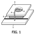
図1は、本発明の第1実施形態を示す。LED半導体本体2、すなわちLEDダイは、サブマウントまたは基板1に配置されており、この構造体の頂部には、蛍光体が混入されたセラミックプレートであるカラー変換プレート3が配置されている。他の光活性または波長シフト素子も想到できよう。
FIG. 1 shows a first embodiment of the present invention. The
LED本体2には、例えば導電性接着剤によりカラー変換プレート3を接着できる。
The
この実施形態では、カラー変換プレートまたはキャップ3を介してLEDの少なくとも1つの電気コンタクト8を接触できるように、機能素子、例えばカラー変換プレート(CCP)またはキャップ3内に、少なくとも1つの開口部5が配置されている。このことは、例えば接合ワイヤー4を設置する極めて容易な方法である。しかしながら、下記の製造方法に記載されているように、このことは、この開口部5を通して接合ワイヤー4のコンタクトをハンダ付けするための構造的な基本的特徴とすることもできる。
In this embodiment, at least one
従って、LED半導体は、ワイヤー接合されたタイプの半導体であり、底部には1つの電気コンタクトが設けられているが、見ることはできない。この第1コンタクト、すなわちワイヤーはサブマウント1に接触している。カラー変換器3は、センタリングされた開口部5を有し、この開口部を通して第2の、すなわち可視接合ワイヤー4が導かれている。この開口部5を通して上記物理的プロセスによってカラー変換されない安定した所定量の基本ポンピング波長光を導くことによって、開口部5を同時に使用できる。この第1量の変換されない基本光は、カラー変換プレートの閉じた横断面を通過してくる変換された量の光と混合される。カラー変換プレートの上方には、図示されていないレンズ本体が配置されており、2つの光のカラーを所定の光温度の白色光に混合するようになっている。
Thus, LED semiconductors are wire-bonded type semiconductors that have one electrical contact at the bottom, but cannot be seen. The first contact, that is, the wire is in contact with the
本発明の構造体は、極めて容易な建設的方法で上記問題を解決し、この結果、上記二重の機能を得るものである。 The structure of the present invention solves the above problem in a very easy constructive manner, and as a result, obtains the above dual function.
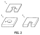
図2は、カラー変換プレートまたはキャップ3の特殊な機能構造のための異なる実施形態を示す。この実施形態では、機能素子、例えばカラー変換プレート(CCP)またはキャップ3内に開口部5として少なくとも1つのスリットが配置されており、カラー変換プレートまたはキャップを介した電気コンタクトの接触を可能にしている。ワイヤーボンディングにより、電気コンタクトが構成された場合、1つのスリットは、CCPを介してワイヤーをLEDの面に導くことにより、CCPによってワイヤーを平面状に配置する魅力的な方法である。かかる配置では、接触LEDから光が出力結合され、電気コンタクト、例えば接合ワイヤーおよび他の機能素子によって妨害されない面(頂部)をLEDプラスCCPに結合できる。
FIG. 2 shows a different embodiment for the special functional structure of the color conversion plate or
図2の上部部分は、所定横断面の面心開口部を有するフラットなカラー変換プレートを示し、この開口部は中心にある開口部からカラー変換プレートの側面まで延びる台形スリット内で終端している。 The upper part of FIG. 2 shows a flat color conversion plate with a face-centered opening of a predetermined cross section, this opening terminating in a trapezoidal slit extending from the central opening to the side of the color conversion plate. .
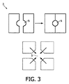
図3は、スプリットまたはセグメント化されたカラー変換プレートまたはキャップ3を使用する実施形態を示す。このプレートまたはキャップの上に、2つのセグメントから成るカラー変換プレート3が示されている。セグメントの2つの平行な面は互いに対向しており、双方の側面は円形開口部5の半円領域を有し、この半円領域はLEDの半導体ダイの頂部に配置された、カラー変換プレートの2つのセグメントをシフトする結果、得られている。従って、この結果得られる円形開口部を通ってガイドされる接合ワイヤーに関し、容易な実装手順も可能となる。まず最初に、ワイヤーを取り付け、異なる側面からプレートレットを後に取り付けることができる。
FIG. 3 shows an embodiment using a split or segmented color conversion plate or
この結果得られる開口部は、セラミックカラー変換プレートまたはギャップ内で構成できる別の輪郭、例えば正方形、楕円形または他の形状ともなり得る。 The resulting opening can also be a ceramic color conversion plate or another contour that can be configured within the gap, such as a square, oval, or other shape.
図3の下方部分は、カラー変換プレートまたはキャップ3が4つのセグメントに分割されている一実施形態を示す。この実施形態は、中心開口部5内で共にシフトされた場合に得られる輪郭を有するセグメントも特徴とする。このバージョンの実施形態では、この開口部を通るように接合ワイヤーを容易にガイドすることもできる。
The lower part of FIG. 3 shows an embodiment in which the color conversion plate or
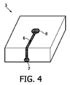
図4は、カラー変換キャップ3を示しており、例えば、気相デポジションにより、LEDダイにキャップを配置した後に、外側表面を示す外側表面の頂部に導電路6を配置する。この導電路は、中心コンタクト部分8の間に配置されており、このコンタクト部分8は、開口部または配置された導電性ビアまたはポストを通して半導体ダイに接触し、このコンタクト部分をLEDに接触させている。導電路6は、この導電路がハンダパッド7内で終わっているキャップ3のサイドラインまで延びている。導電路を別の接合ワイヤーまたは垂直LED構造体のサブマウント上の接続部分に接続するのに、このハンダパッド7が使用される。この導電路を薄い銅の層からエッチングで形成した銅の導電路とすることもでき、この銅の層によってカラー変換プレートをあらかじめカバーすることができる。導電路は極めて薄い導電膜により実現でき、この膜をLEDダイからの光および/または変換された光が通過できる。
FIG. 4 shows the
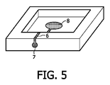
図5には、カラー変換プレートまたはキャップの別の実施形態が示されている。LEDの電気コンタクトはキャップ3の内側面に配置された導電路6によって実現されており、導電路の各端部にはハンダパッド7、8が配置されている。LEDダイに接触するように、プレートまたはキャップの中間には1つのパッドがセンタリングされている。他方のパッドは外側に延び、外側に配置されたサブマントまたは電気手段に電気的に接触するようになっている。
FIG. 5 shows another embodiment of a color conversion plate or cap. The electrical contact of the LED is realized by a
図6は、配置に関する4つの詳細な実施形態を開示しており、一部の実施形態では、導電路が内蔵される一体的な配置を示している。 FIG. 6 discloses four detailed embodiments related to the arrangement, and in some embodiments, shows an integral arrangement with a built-in conductive path.
図6aは、サブマウントまたは基板1より上方において、LEDダイ2全体を収納するキャップ状のカラー変換器3を備えた垂直LED構造体を示す。中心開口部を通して接合ワイヤー4をガイドするように、中心開口部5が配置されている。更に、この開口部によって、変換されないポンピング波長の光の一定の放出を可能にしている。
FIG. 6 a shows a vertical LED structure with a cap-shaped
図6bは、カラー変換キャップ3内に所定の開口部を有しない、図6aと同じ構造体を示す。この実施形態では、キャップ3の外側表面に導電路6が配置されているが、この導電路はこの外側表面の頂部に密に配置されており、図6aから分かるように、ワイヤーとしては配置されていない。キャップの表の表面だけにセンタリングされた状態で、ある種の導電ポストまたはビアが配置されており、このビアはLEDダイに電気的に接触している内側ハンダパッド8、すなわちコンタクトパッドまで、上方向にキャップを貫通して延びている。
FIG. 6 b shows the same structure as FIG. 6 a without the predetermined opening in the
図6cは、図5に示された詳細なキャップ状構造体の側面図を示す。導電路6は主にキャップ3の内側表面の内部に配置されており、この導電路6は側面のまわりに配置され、ハンダ付けされたワイヤーまたはサブマウント上のコンタクト手段に直接接触すべき、キャップの側面にあるハンダパッド7だけの上の外側面近くで終わっている。
6c shows a side view of the detailed cap-like structure shown in FIG. The
図6dは、特別な実施形態を示す。この実施形態では、カラー変換キャップ3のバルク内に導電路6が一体化されている。この導電性部分は、例えばワイヤーの一部とすることができる。カラー変換器は、この特別な実施形態だけでなく、図6に示された別の実施形態においても簡単なプレートとすることもできる。導電手段の配置も同様である。この導電手段は、図6cに示された例と平行となっているが、バルク内、すなわちキャップまたはプレートバルクの内部に配置されている。これら導電路の端部は、図6cに示されるようなハンダまたはコンタクトパッドとして形成されている。
FIG. 6d shows a special embodiment. In this embodiment, the
図6b〜6dの実施形態は、開口部を示しておらず、図6aでは、所定の変換されないポンピング波長の光を放出するために、図6aの実施形態を同時に使用できる。カラー変換プレートまたはキャップは、図6b〜6dの実施形態では、中間濃度の蛍光体または他の光活性材だけから成る。従って、カラー変換プロセスの光活性波長シフトは、明らかに100%未満の効率である。この結果、ある量の変換された光とある量の変換されていない光の双方が放出される。従って、合計はほとんど100%となる。 The embodiment of FIGS. 6b-6d does not show an opening, and in FIG. 6a, the embodiment of FIG. 6a can be used simultaneously to emit light of a predetermined unconverted pumping wavelength. The color conversion plate or cap, in the embodiment of FIGS. 6b-6d, consists only of an intermediate concentration of phosphor or other photoactive material. Thus, the photoactive wavelength shift of the color conversion process is clearly less than 100% efficient. This results in both an amount of converted light and an amount of unconverted light being emitted. Therefore, the total is almost 100%.
図7は、本明細書に記載し、請求項に請求する製造方法のステップを示すことができるように、最終的には実装されないLEDをより詳細に示す。LED外の表面の頂部には導電路6が一体的に実装されたカラー変換器3が配置されており、この導電路6は、カラー変換プレート3の内部に明らかに進入することにより、はカラー変換プレート3の開口部5の内部で終端している。LEDダイの表面の頂部に変換プレート3が位置する場合、この開口部5を通過し、導電路とLEDダイの頂部の上のコンタクト領域との間に、電気接続部を形成するようハンダ付けステップまたは溶接ステップを実行する。次に、この開口部を閉じることができるので、この方法によって形成される実施形態は、図6a〜6dの実施形態で使用さるようなカラー変換材料を使用する。
FIG. 7 shows in more detail the LED that will ultimately not be implemented so that it can illustrate the steps of the manufacturing method described and claimed herein. A
図8には、垂直LED構造体を実装する別の方法も含む、別の実施形態が示されている。機能素子、この場合カラー変換器3は、カラー変換プレートまたはキャップ3の表面内にキャビティ9を備え、この表面はLED半導体チップに向いており、および/またはLED半導体チップ(=CCPの内側表面)に接着されている。LED半導体チップの頂部上のハンダパッド6から、LED+CCP装置の外側に向かって、このキャビティ9内に接合ワイヤーのような電気コンタクトを配置できる。このような解決方法は、特に接合ワイヤーを有するLEDに対して重要である。この接合ワイヤーは、平らなLED半導体表面にフラットな変換プレートまたはキャップを機械的に誤った取り付けを誘導することなく、キャビティ9内に接合ワイヤーを容易に配置できる。
FIG. 8 illustrates another embodiment that also includes another method of implementing a vertical LED structure. The functional element, in this case the
LEDダイのコンタクト領域をドロップのほぼ半分の構造体によりハンダ付けする。この方法の間、極めて小さい入射角で接合ワイヤーをハンダ付けする。一部のケースでは、30°未満の角度を許容できるが、10°未満の角度が極めて好ましい。従って、LEDダイをできるだけ密に取り付けながら、キャビティ9をせできるだけフラットにできる。ライン形状の別のキャビティまたは溝10が、接合ワイヤーを構造体から側面までガイドするので、この接合ワイヤーをサブマウント1に外側から接合できる。
The contact area of the LED die is soldered with approximately half the structure of the drop. During this method, the bonding wire is soldered with a very small angle of incidence. In some cases, angles less than 30 ° can be tolerated, but angles less than 10 ° are highly preferred. Therefore, the
この実施形態は、部分ポンピング波長発光のための開口部を用いない、閉じたカラー変換プレートまたはキャップ3も備える。
This embodiment also comprises a closed color conversion plate or
1 基板
2 LED半導体本体
3 カラー変換プレート
4 接合ワイヤー
5 開口部
6 導電路
7 ハンダパッド
8 電気コンタクト
9 キャビティ
DESCRIPTION OF
Claims (16)
Applications Claiming Priority (2)
| Application Number | Priority Date | Filing Date | Title |
|---|---|---|---|
| EP05107760 | 2005-08-24 | ||
| PCT/IB2006/052797 WO2007023411A1 (en) | 2005-08-24 | 2006-08-14 | Light emitting diodes and lasers diodes with color converters |
Publications (2)
| Publication Number | Publication Date |
|---|---|
| JP2009506527A true JP2009506527A (en) | 2009-02-12 |
| JP2009506527A5 JP2009506527A5 (en) | 2009-10-01 |
Family
ID=37547491
Family Applications (1)
| Application Number | Title | Priority Date | Filing Date |
|---|---|---|---|
| JP2008527548A Pending JP2009506527A (en) | 2005-08-24 | 2006-08-14 | Electrical contact system for light emitting diodes and laser diodes with color converter |
Country Status (7)
| Country | Link |
|---|---|
| US (1) | US7863642B2 (en) |
| EP (1) | EP1922764A1 (en) |
| JP (1) | JP2009506527A (en) |
| KR (1) | KR20080048492A (en) |
| CN (1) | CN101248535B (en) |
| TW (1) | TW200715254A (en) |
| WO (1) | WO2007023411A1 (en) |
Cited By (3)
| Publication number | Priority date | Publication date | Assignee | Title |
|---|---|---|---|---|
| JP2014090164A (en) * | 2012-10-29 | 2014-05-15 | Lg Innotek Co Ltd | Light-emitting element and light-emitting element package |
| JP2015046513A (en) * | 2013-08-28 | 2015-03-12 | 日亜化学工業株式会社 | Wavelength conversion member, light-emitting device, and method of manufacturing light-emitting device |
| JP2020536372A (en) * | 2017-09-28 | 2020-12-10 | ソラア レイザー ダイオード インク | Intelligent visible light with gallium and nitrogen-containing laser sources |
Families Citing this family (17)
| Publication number | Priority date | Publication date | Assignee | Title |
|---|---|---|---|---|
| WO2008152552A1 (en) * | 2007-06-13 | 2008-12-18 | Philips Intellectual Property & Standards Gmbh | Led lighting device |
| US9401461B2 (en) * | 2007-07-11 | 2016-07-26 | Cree, Inc. | LED chip design for white conversion |
| US7859000B2 (en) * | 2008-04-10 | 2010-12-28 | Cree, Inc. | LEDs using single crystalline phosphor and methods of fabricating same |
| JP5255421B2 (en) * | 2008-12-15 | 2013-08-07 | 株式会社小糸製作所 | Light emitting module, method for manufacturing light emitting module, and lamp unit |
| JP2010219166A (en) * | 2009-03-13 | 2010-09-30 | Nippon Electric Glass Co Ltd | Semiconductor light emitting element device |
| WO2010143114A1 (en) | 2009-06-11 | 2010-12-16 | Koninklijke Philips Electronics N.V. | Led illumination device |
| US20110062468A1 (en) * | 2009-09-11 | 2011-03-17 | Koninklijke Philips Electronics N.V. | Phosphor-converted light emitting diode device |
| DE102009042205A1 (en) * | 2009-09-18 | 2011-03-31 | Osram Opto Semiconductors Gmbh | Optoelectronic module |
| DE102010022561A1 (en) * | 2010-06-02 | 2011-12-08 | Osram Opto Semiconductors Gmbh | Wavelength conversion element, optoelectronic component with a wavelength conversion element and method for producing a wavelength conversion element |
| DE102010035490A1 (en) * | 2010-08-26 | 2012-03-01 | Osram Opto Semiconductors Gmbh | Radiation-emitting component and method for producing a radiation-emitting component |
| TW201217706A (en) * | 2010-10-26 | 2012-05-01 | Wistron Corp | Light emitting apparatus and using method thereof |
| DE102011077644A1 (en) * | 2011-06-16 | 2012-12-20 | Osram Ag | Illuminating device for e.g. video projector, has bonding wires which are provided between contact surface of n-polarized semiconductor light-emitting chip and front-side surface of metallization region |
| CN104160212B (en) | 2012-03-01 | 2018-10-12 | 飞利浦灯具控股公司 | LED illumination is arranged |
| DE102012101892B4 (en) | 2012-03-06 | 2021-05-12 | OSRAM Opto Semiconductors Gesellschaft mit beschränkter Haftung | Wavelength conversion element, light-emitting semiconductor component and display device therewith as well as method for producing a wavelength conversion element |
| DE102013009444A1 (en) * | 2013-05-31 | 2014-12-04 | Jenoptik Polymer Systems Gmbh | Substrate and / or component for the protection of at least one bonding wire |
| DE102017119346A1 (en) * | 2017-08-24 | 2019-02-28 | Osram Opto Semiconductors Gmbh | Component with buffer layer and method for producing a component |
| DE102022101910A1 (en) * | 2022-01-27 | 2023-07-27 | OSRAM Opto Semiconductors Gesellschaft mit beschränkter Haftung | OPTOELECTRONIC SEMICONDUCTOR COMPONENT, CONVERSION ELEMENT AND MANUFACTURING PROCESS |
Citations (7)
| Publication number | Priority date | Publication date | Assignee | Title |
|---|---|---|---|---|
| JPH0832118A (en) * | 1994-07-19 | 1996-02-02 | Rohm Co Ltd | Light emitting diode |
| JPH08227908A (en) * | 1994-12-20 | 1996-09-03 | Hitachi Ltd | Semiconductor device and manufacture thereof |
| WO1997050132A1 (en) * | 1996-06-26 | 1997-12-31 | Siemens Aktiengesellschaft | Light-emitting semiconductor component with luminescence conversion element |
| JPH11297738A (en) * | 1998-04-06 | 1999-10-29 | Denso Corp | Structure for mounting of semiconductor chip on substrate |
| JP2000068405A (en) * | 1998-08-20 | 2000-03-03 | Nec Corp | Semiconductor device and manufacture thereof |
| JP2003258312A (en) * | 2002-03-01 | 2003-09-12 | Citizen Electronics Co Ltd | Method for manufacturing light emitting device |
| JP2004172578A (en) * | 2002-09-02 | 2004-06-17 | Matsushita Electric Ind Co Ltd | Light-emitting device |
Family Cites Families (16)
| Publication number | Priority date | Publication date | Assignee | Title |
|---|---|---|---|---|
| JPS63164482A (en) | 1986-12-26 | 1988-07-07 | Res Dev Corp Of Japan | Light emitting diode device |
| US5149958A (en) | 1990-12-12 | 1992-09-22 | Eastman Kodak Company | Optoelectronic device component package |
| DE19527026C2 (en) | 1995-07-24 | 1997-12-18 | Siemens Ag | Optoelectronic converter and manufacturing process |
| TW406442B (en) | 1998-07-09 | 2000-09-21 | Sumitomo Electric Industries | White colored LED and intermediate colored LED |
| CA2312646A1 (en) * | 2000-06-28 | 2001-12-28 | Institut National D'optique | Hybrid micropackaging of microdevices |
| JP4055405B2 (en) * | 2001-12-03 | 2008-03-05 | ソニー株式会社 | Electronic component and manufacturing method thereof |
| US20030141563A1 (en) * | 2002-01-28 | 2003-07-31 | Bily Wang | Light emitting diode package with fluorescent cover |
| US20040032728A1 (en) * | 2002-08-19 | 2004-02-19 | Robert Galli | Optical assembly for LED chip package |
| US7078737B2 (en) | 2002-09-02 | 2006-07-18 | Matsushita Electric Industrial Co., Ltd. | Light-emitting device |
| JP2004128057A (en) * | 2002-09-30 | 2004-04-22 | Fuji Photo Film Co Ltd | Light emitting device and its manufacturing method |
| US6885033B2 (en) | 2003-03-10 | 2005-04-26 | Cree, Inc. | Light emitting devices for light conversion and methods and semiconductor chips for fabricating the same |
| JP2004342870A (en) | 2003-05-16 | 2004-12-02 | Stanley Electric Co Ltd | Light emitting diode to be driven with large current |
| KR20050034936A (en) * | 2003-10-10 | 2005-04-15 | 삼성전기주식회사 | Wavelength - converted light emitting diode package using phosphor and manufacturing method |
| KR100613273B1 (en) | 2003-12-30 | 2006-08-18 | 주식회사 이츠웰 | Light emitting diode with vertical electrode structure and manufacturing method of the same |
| US7355284B2 (en) | 2004-03-29 | 2008-04-08 | Cree, Inc. | Semiconductor light emitting devices including flexible film having therein an optical element |
| KR100662844B1 (en) | 2005-06-10 | 2007-01-02 | 삼성전자주식회사 | Led package structure and manufacturing method, and led array module |
-
2006
- 2006-08-14 EP EP06795650A patent/EP1922764A1/en not_active Withdrawn
- 2006-08-14 CN CN2006800307988A patent/CN101248535B/en not_active Expired - Fee Related
- 2006-08-14 US US12/064,097 patent/US7863642B2/en not_active Expired - Fee Related
- 2006-08-14 WO PCT/IB2006/052797 patent/WO2007023411A1/en active Application Filing
- 2006-08-14 JP JP2008527548A patent/JP2009506527A/en active Pending
- 2006-08-14 KR KR1020087006937A patent/KR20080048492A/en not_active Application Discontinuation
- 2006-08-21 TW TW095130688A patent/TW200715254A/en unknown
Patent Citations (7)
| Publication number | Priority date | Publication date | Assignee | Title |
|---|---|---|---|---|
| JPH0832118A (en) * | 1994-07-19 | 1996-02-02 | Rohm Co Ltd | Light emitting diode |
| JPH08227908A (en) * | 1994-12-20 | 1996-09-03 | Hitachi Ltd | Semiconductor device and manufacture thereof |
| WO1997050132A1 (en) * | 1996-06-26 | 1997-12-31 | Siemens Aktiengesellschaft | Light-emitting semiconductor component with luminescence conversion element |
| JPH11297738A (en) * | 1998-04-06 | 1999-10-29 | Denso Corp | Structure for mounting of semiconductor chip on substrate |
| JP2000068405A (en) * | 1998-08-20 | 2000-03-03 | Nec Corp | Semiconductor device and manufacture thereof |
| JP2003258312A (en) * | 2002-03-01 | 2003-09-12 | Citizen Electronics Co Ltd | Method for manufacturing light emitting device |
| JP2004172578A (en) * | 2002-09-02 | 2004-06-17 | Matsushita Electric Ind Co Ltd | Light-emitting device |
Cited By (6)
| Publication number | Priority date | Publication date | Assignee | Title |
|---|---|---|---|---|
| JP2014090164A (en) * | 2012-10-29 | 2014-05-15 | Lg Innotek Co Ltd | Light-emitting element and light-emitting element package |
| JP2015046513A (en) * | 2013-08-28 | 2015-03-12 | 日亜化学工業株式会社 | Wavelength conversion member, light-emitting device, and method of manufacturing light-emitting device |
| JP2020536372A (en) * | 2017-09-28 | 2020-12-10 | ソラア レイザー ダイオード インク | Intelligent visible light with gallium and nitrogen-containing laser sources |
| JP7052020B2 (en) | 2017-09-28 | 2022-04-11 | キョウセラ エスエルディー レイザー,インコーポレイテッド | Light source with gallium and nitrogen containing laser source and integrated white light source |
| US11677468B2 (en) | 2017-09-28 | 2023-06-13 | Kyocera Sld Laser, Inc. | Laser based white light source configured for communication |
| US11870495B2 (en) | 2017-09-28 | 2024-01-09 | Kyocera Sld Laser, Inc. | Intelligent visible light with a gallium and nitrogen containing laser source |
Also Published As
| Publication number | Publication date |
|---|---|
| US7863642B2 (en) | 2011-01-04 |
| EP1922764A1 (en) | 2008-05-21 |
| KR20080048492A (en) | 2008-06-02 |
| CN101248535A (en) | 2008-08-20 |
| TW200715254A (en) | 2007-04-16 |
| WO2007023411A1 (en) | 2007-03-01 |
| US20080232420A1 (en) | 2008-09-25 |
| CN101248535B (en) | 2011-09-07 |
Similar Documents
| Publication | Publication Date | Title |
|---|---|---|
| JP2009506527A (en) | Electrical contact system for light emitting diodes and laser diodes with color converter | |
| US9006761B2 (en) | Light-emitting device | |
| JP5698496B2 (en) | Light emitting chip, LED package, backlight for liquid crystal display, liquid crystal display and illumination | |
| JP4535928B2 (en) | Semiconductor light emitting device | |
| US7598528B2 (en) | High power light emitting diode package and method of producing the same | |
| JP2007080872A (en) | Light emitting device | |
| JP2007180430A (en) | Light-emitting diode device | |
| KR101271373B1 (en) | Semiconductor composite device and method of manufacturing the same | |
| US8461609B2 (en) | Light emitting device package | |
| JP3941826B2 (en) | LED luminaire manufacturing method | |
| JP5484544B2 (en) | Light emitting device | |
| JP2005333014A (en) | Led lamp | |
| KR20070036375A (en) | White light emitting device package | |
| JP5179311B2 (en) | Light emitting device | |
| KR20130012704A (en) | White light-emitting diode and method of manufacturing the same | |
| US20170141272A1 (en) | Frame for semiconductor light emitting device | |
| KR20110131429A (en) | Light emitting device and method of manufacturing the same | |
| KR20090132916A (en) | Light emitting device | |
| KR100610272B1 (en) | Multi Color LED With Wide Directivity Structure | |
| KR101806790B1 (en) | Semiconductor light emitting device | |
| KR101772551B1 (en) | Semiconductor light emitting structure and method of manufacturing the same | |
| KR20170036295A (en) | Semiconductor light emitting device and method of manufacturing the same | |
| JP2013191883A (en) | Semiconductor light emitting device | |
| JP4737218B2 (en) | Method for manufacturing light emitting device | |
| JP2007180329A (en) | Light-emitting diode lighting device |
Legal Events
| Date | Code | Title | Description |
|---|---|---|---|
| A521 | Request for written amendment filed |
Free format text: JAPANESE INTERMEDIATE CODE: A523 Effective date: 20090811 |
|
| A621 | Written request for application examination |
Free format text: JAPANESE INTERMEDIATE CODE: A621 Effective date: 20090811 |
|
| A131 | Notification of reasons for refusal |
Free format text: JAPANESE INTERMEDIATE CODE: A131 Effective date: 20120416 |
|
| A02 | Decision of refusal |
Free format text: JAPANESE INTERMEDIATE CODE: A02 Effective date: 20120918 |