JP2009295932A - Exposure device and device manufacturing method - Google Patents
Exposure device and device manufacturing method Download PDFInfo
- Publication number
- JP2009295932A JP2009295932A JP2008150836A JP2008150836A JP2009295932A JP 2009295932 A JP2009295932 A JP 2009295932A JP 2008150836 A JP2008150836 A JP 2008150836A JP 2008150836 A JP2008150836 A JP 2008150836A JP 2009295932 A JP2009295932 A JP 2009295932A
- Authority
- JP
- Japan
- Prior art keywords
- substrate
- measurement
- stage
- exposure
- exposure apparatus
- Prior art date
- Legal status (The legal status is an assumption and is not a legal conclusion. Google has not performed a legal analysis and makes no representation as to the accuracy of the status listed.)
- Pending
Links
Images


Classifications
-
- G—PHYSICS
- G03—PHOTOGRAPHY; CINEMATOGRAPHY; ANALOGOUS TECHNIQUES USING WAVES OTHER THAN OPTICAL WAVES; ELECTROGRAPHY; HOLOGRAPHY
- G03F—PHOTOMECHANICAL PRODUCTION OF TEXTURED OR PATTERNED SURFACES, e.g. FOR PRINTING, FOR PROCESSING OF SEMICONDUCTOR DEVICES; MATERIALS THEREFOR; ORIGINALS THEREFOR; APPARATUS SPECIALLY ADAPTED THEREFOR
- G03F7/00—Photomechanical, e.g. photolithographic, production of textured or patterned surfaces, e.g. printing surfaces; Materials therefor, e.g. comprising photoresists; Apparatus specially adapted therefor
- G03F7/70—Microphotolithographic exposure; Apparatus therefor
- G03F7/70483—Information management; Active and passive control; Testing; Wafer monitoring, e.g. pattern monitoring
- G03F7/70491—Information management, e.g. software; Active and passive control, e.g. details of controlling exposure processes or exposure tool monitoring processes
- G03F7/70508—Data handling in all parts of the microlithographic apparatus, e.g. handling pattern data for addressable masks or data transfer to or from different components within the exposure apparatus
-
- G—PHYSICS
- G03—PHOTOGRAPHY; CINEMATOGRAPHY; ANALOGOUS TECHNIQUES USING WAVES OTHER THAN OPTICAL WAVES; ELECTROGRAPHY; HOLOGRAPHY
- G03F—PHOTOMECHANICAL PRODUCTION OF TEXTURED OR PATTERNED SURFACES, e.g. FOR PRINTING, FOR PROCESSING OF SEMICONDUCTOR DEVICES; MATERIALS THEREFOR; ORIGINALS THEREFOR; APPARATUS SPECIALLY ADAPTED THEREFOR
- G03F7/00—Photomechanical, e.g. photolithographic, production of textured or patterned surfaces, e.g. printing surfaces; Materials therefor, e.g. comprising photoresists; Apparatus specially adapted therefor
- G03F7/70—Microphotolithographic exposure; Apparatus therefor
- G03F7/70216—Mask projection systems
- G03F7/70358—Scanning exposure, i.e. relative movement of patterned beam and workpiece during imaging
-
- G—PHYSICS
- G03—PHOTOGRAPHY; CINEMATOGRAPHY; ANALOGOUS TECHNIQUES USING WAVES OTHER THAN OPTICAL WAVES; ELECTROGRAPHY; HOLOGRAPHY
- G03F—PHOTOMECHANICAL PRODUCTION OF TEXTURED OR PATTERNED SURFACES, e.g. FOR PRINTING, FOR PROCESSING OF SEMICONDUCTOR DEVICES; MATERIALS THEREFOR; ORIGINALS THEREFOR; APPARATUS SPECIALLY ADAPTED THEREFOR
- G03F7/00—Photomechanical, e.g. photolithographic, production of textured or patterned surfaces, e.g. printing surfaces; Materials therefor, e.g. comprising photoresists; Apparatus specially adapted therefor
- G03F7/70—Microphotolithographic exposure; Apparatus therefor
- G03F7/70483—Information management; Active and passive control; Testing; Wafer monitoring, e.g. pattern monitoring
- G03F7/70491—Information management, e.g. software; Active and passive control, e.g. details of controlling exposure processes or exposure tool monitoring processes
- G03F7/70525—Controlling normal operating mode, e.g. matching different apparatus, remote control or prediction of failure
-
- G—PHYSICS
- G03—PHOTOGRAPHY; CINEMATOGRAPHY; ANALOGOUS TECHNIQUES USING WAVES OTHER THAN OPTICAL WAVES; ELECTROGRAPHY; HOLOGRAPHY
- G03F—PHOTOMECHANICAL PRODUCTION OF TEXTURED OR PATTERNED SURFACES, e.g. FOR PRINTING, FOR PROCESSING OF SEMICONDUCTOR DEVICES; MATERIALS THEREFOR; ORIGINALS THEREFOR; APPARATUS SPECIALLY ADAPTED THEREFOR
- G03F7/00—Photomechanical, e.g. photolithographic, production of textured or patterned surfaces, e.g. printing surfaces; Materials therefor, e.g. comprising photoresists; Apparatus specially adapted therefor
- G03F7/70—Microphotolithographic exposure; Apparatus therefor
- G03F7/70691—Handling of masks or workpieces
- G03F7/70716—Stages
- G03F7/70725—Stages control
-
- G—PHYSICS
- G03—PHOTOGRAPHY; CINEMATOGRAPHY; ANALOGOUS TECHNIQUES USING WAVES OTHER THAN OPTICAL WAVES; ELECTROGRAPHY; HOLOGRAPHY
- G03F—PHOTOMECHANICAL PRODUCTION OF TEXTURED OR PATTERNED SURFACES, e.g. FOR PRINTING, FOR PROCESSING OF SEMICONDUCTOR DEVICES; MATERIALS THEREFOR; ORIGINALS THEREFOR; APPARATUS SPECIALLY ADAPTED THEREFOR
- G03F7/00—Photomechanical, e.g. photolithographic, production of textured or patterned surfaces, e.g. printing surfaces; Materials therefor, e.g. comprising photoresists; Apparatus specially adapted therefor
- G03F7/70—Microphotolithographic exposure; Apparatus therefor
- G03F7/70691—Handling of masks or workpieces
- G03F7/70775—Position control, e.g. interferometers or encoders for determining the stage position
-
- H—ELECTRICITY
- H01—ELECTRIC ELEMENTS
- H01L—SEMICONDUCTOR DEVICES NOT COVERED BY CLASS H10
- H01L21/00—Processes or apparatus adapted for the manufacture or treatment of semiconductor or solid state devices or of parts thereof
- H01L21/67—Apparatus specially adapted for handling semiconductor or electric solid state devices during manufacture or treatment thereof; Apparatus specially adapted for handling wafers during manufacture or treatment of semiconductor or electric solid state devices or components ; Apparatus not specifically provided for elsewhere
- H01L21/67005—Apparatus not specifically provided for elsewhere
- H01L21/67242—Apparatus for monitoring, sorting or marking
- H01L21/67259—Position monitoring, e.g. misposition detection or presence detection
Abstract
Description
本発明は、露光装置及びデバイス製造方法に関する。 The present invention relates to an exposure apparatus and a device manufacturing method.
半導体露光装置において、ステッパと呼ばれるステップ・アンド・リピート方式の露光装置が現在主流となっている。ステッパは、基板を所定の場所に位置決めして静止させた状態で、パターンが描画された原版を通った光を投影光学系にて一定の比率で縮小し、基板上に塗布された感光剤を感光させて原版のパターンを基板に転写する。基板を支持する基板ステージを逐次駆動させることで、この行程を基板全面にわたって繰り返し行う。基板はウエハとも、原版はレチクルとも、感光剤はレジストとも称される。 In a semiconductor exposure apparatus, a step-and-repeat type exposure apparatus called a stepper is currently mainstream. The stepper is a state where the substrate is positioned at a predetermined position and is stationary, and the light passing through the original on which the pattern is drawn is reduced at a certain ratio by the projection optical system, and the photosensitive agent applied on the substrate is reduced. The pattern of the original is transferred to the substrate by exposing it to light. This process is repeated over the entire surface of the substrate by sequentially driving the substrate stage that supports the substrate. The substrate is also called a wafer, the original plate is called a reticle, and the photosensitive agent is called a resist.
ウエハを静止して一括露光するステッパに対し、スキャナと称されるステップ・アンド・スキャン方式の露光装置は、ウエハ及びレチクルを同期走査(スキャン)させながら、より広い領域を露光する。 A step-and-scan exposure apparatus called a scanner exposes a wider area while synchronously scanning (scanning) the wafer and reticle with respect to a stepper that performs batch exposure with the wafer stationary.
通常、露光装置を用いた半導体の製造では、同じウエハに対して何度も露光の行程を行う必要がある。つまり、すでにパターンが形成されたショットに対して、別のパターンを精度よく重ねて露光する必要がある。そのためには、ショットの配列を、事前に計測しておく必要がある。パターンに計測用のマークを事前に入れておき、スコープを使ってこの計測用のマークが計測されうる。スコープとして、非露光光を用いたオフアクシススコープ(以下、OASと略す)を用いるのが一般的である。非露光光であるため、レジストを感光させずに計測を行うことができるが、投影光学系を通すことができないため、投影光学系とは離れて配置する必要がある(図6参照)。 Usually, in the manufacture of a semiconductor using an exposure apparatus, it is necessary to repeatedly perform the exposure process on the same wafer. In other words, it is necessary to expose another pattern with high accuracy with respect to a shot in which a pattern has already been formed. For this purpose, it is necessary to measure the arrangement of shots in advance. A measurement mark can be put in the pattern in advance, and the measurement mark can be measured using a scope. As the scope, an off-axis scope (hereinafter abbreviated as OAS) using non-exposure light is generally used. Since it is non-exposure light, measurement can be performed without exposing the resist, but it cannot pass through the projection optical system, so it must be arranged away from the projection optical system (see FIG. 6).
通常、スキャナでは、投影光学系の下で露光するとき、駆動を行いながらフォーカス合わせする、リアルタイムフォーカスを行う。図6に示されるように、実際の露光位置(スリット)の前後、つまりY方向にシフトしたところにフォーカスセンサ6A,6Cを配置する。ステージが紙面の下方から走査(スキャン)されて露光するときは、6Cのフォーカスセンサでウエハ表面のZ位置を露光前に計測し、露光位置がスリット位置にくる前にステージをZ方向に駆動させる。紙面の上方からステージがスキャンされるときには、同様に、6Aのフォーカスセンサを用いる。スリットの下でウエハ表面が投影光学系のレンズ像面に追い込まれたかを確認するために、スリット位置にもフォーカスセンサ6Bが配置されている。また、センサをX方向に複数配置することで、スリット内のウエハ表面の傾きも検出できる。このように、露光直前にフォーカスを計測するため、ウエハ全面のフォーカスを予め計測しなくてすみ、スループットが低下しない。
Normally, a scanner performs real-time focusing, in which focusing is performed while driving when exposure is performed under a projection optical system. As shown in FIG. 6,
OASを用いた露光シーケンスは、以下の通りである。ウエハが搬送されると、ウエハ上の各サンプルショットの事前に決めておいたマークを、OASを使って計測する。その計測結果から、ウエハの置き誤差(XY、回転成分)や、熱膨張による誤差を算出する。そして、投影光学系のレンズの下にウエハを移動させて、各ショットを露光する。サンプルショットが多ければ、重ね合わせの精度は向上するが、スループットは低下する。また、1ショット内に複数の計測マークを配置し、これを計測することで、ショットの形状に合わせた露光も可能となり、重ね合わせ精度はさらに向上するが、やはり、スループットは低下する。 The exposure sequence using OAS is as follows. When the wafer is transported, a predetermined mark of each sample shot on the wafer is measured using OAS. From the measurement results, a wafer placement error (XY, rotational component) and an error due to thermal expansion are calculated. Then, the wafer is moved under the lens of the projection optical system to expose each shot. If there are many sample shots, the overlay accuracy is improved, but the throughput is lowered. In addition, by arranging a plurality of measurement marks in one shot and measuring them, it becomes possible to perform exposure according to the shape of the shot and further improve the overlay accuracy, but the throughput also decreases.
サンプルショットの計測と露光とを同時に行い、スループットと精度とを向上させるための方式として、ウエハステージを2つ用意し、片方が露光を行っているときに、他方でOASによる計測を行う方式がある(図7参照)。この方式をツインステージ構成と称す。対照的に、ステージが1つの方式を、シングルステージ構成と称す。 As a method for performing sample shot measurement and exposure at the same time to improve throughput and accuracy, there is a method in which two wafer stages are prepared and one is performing exposure and the other is performing measurement by OAS. Yes (see FIG. 7). This method is called a twin stage configuration. In contrast, a system with one stage is referred to as a single stage configuration.
ツインステージ構成では、ウエハがロードされると、まず、OASによってショットのXYの位置ずれが計測される。次に、フォーカスセンサがウエハ全面を計測する。このとき、もう片方のウエハステージは、投影光学系のレンズの下にいる。計測が終了したウエハを保持したまま、投影光学系のレンズの下にウエハステージを持って行き、露光を開始する。このとき、他方のウエハステージをOAS位置に駆動し、同様に、ウエハロード、OAS計測、フォーカス計測を、露光と並列して実行する。OAS計測やフォーカス計測が、露光するまでに終了していれば、仮にサンプルショットを増やしたとしても、スループットを悪化させることはない。よって、スループットと精度とを両立させることができる。 In the twin stage configuration, when a wafer is loaded, first, the XY positional deviation of the shot is measured by OAS. Next, the focus sensor measures the entire wafer surface. At this time, the other wafer stage is under the lens of the projection optical system. While holding the wafer whose measurement has been completed, the wafer stage is brought under the lens of the projection optical system, and exposure is started. At this time, the other wafer stage is driven to the OAS position, and similarly, wafer loading, OAS measurement, and focus measurement are executed in parallel with exposure. If OAS measurement and focus measurement are completed before exposure, even if the number of sample shots is increased, the throughput is not deteriorated. Therefore, both throughput and accuracy can be achieved.
フォーカスセンサは、通常X方向に並んだ構成をとる。これは、Y方向にスキャンしたときに、より多くの幅を計測することで、計測時間を短縮するためである。また、後述するレーザ干渉計は、レンズ位置、OAS位置のそれぞれに配置される。 The focus sensors are usually arranged in the X direction. This is to reduce the measurement time by measuring a larger width when scanning in the Y direction. Further, a laser interferometer described later is disposed at each of the lens position and the OAS position.
ウエハステージは、2次元平面(XY平面)内の任意の場所に高精度かつ広範囲に亙って駆動されることが要求される。この理由の1つは、半導体回路の微細化が進むにつれ、必要とされる精度がますます厳しいものとなることである。他の理由は、ウエハの大口径化、ウエハを交換するための交換位置への駆動、ウエハに露光されたマークを露光位置以外で計測する場合等、ウエハステージが駆動する領域も、非常に広範囲にわたる必要があるためである。 The wafer stage is required to be driven over a wide range with high accuracy to an arbitrary place in a two-dimensional plane (XY plane). One reason for this is that the required accuracy becomes increasingly severe as semiconductor circuits become more miniaturized. Other reasons include an extremely wide area for driving the wafer stage, such as increasing the diameter of the wafer, driving to an exchange position for exchanging the wafer, and measuring marks exposed on the wafer other than the exposure position. It is necessary to span.
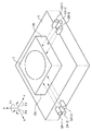
ウエハステージの位置を検出するために、レーザ干渉計が一般的に用いられている。このレーザ干渉計をXY平面内に配置することで、ウエハステージのXY平面内の位置を計測することができる。例えば、図1のように、ウエハステージ1には、X軸計測用の平面鏡2A(以下、バーミラーと称す)がY軸方向に沿って搭載されうる。X軸方向の位置を計測するレーザ干渉計3A−1は、X軸に略平行にレーザをバーミラー2Aに照射して、その反射光と基準光とを干渉させることで、ウエハステージの相対的な駆動量を検出している。Y軸方向の位置の計測も同様である。X軸、Y軸のどちらか、又は、両方の干渉計を2つ用意することで、ウエハステージのZ軸周りの回転角θzも検出することができる。
In order to detect the position of the wafer stage, a laser interferometer is generally used. By arranging this laser interferometer in the XY plane, the position of the wafer stage in the XY plane can be measured. For example, as shown in FIG. 1, a
レーザ干渉計から得られた位置情報を基に、リニアモータなどのアクチュエータ(図示せず)をXY平面に配置することによって、ウエハステージを所定の場所に駆動することができる。 The wafer stage can be driven to a predetermined location by arranging an actuator (not shown) such as a linear motor on the XY plane based on the position information obtained from the laser interferometer.
回路の微細化に伴うレンズの高NA化に伴い、レチクルの像をウエハに転写するためのフォーカス許容範囲(焦点深度)も狭くなり、フォーカス方向(Z方向)の位置決めに要求される精度は厳しくなってきている。そのため、ステージは、XY平面に直交するZ方向(フォーカス方向)、及び、X軸方向に関する傾斜、Y軸方向への傾斜も、高精度に計測し制御する必要がある。X軸方向に関する傾斜はY軸周りの回転であり、チルトあるいはθyと称される。Y軸方向への傾斜はX軸周りの回転であり、チルトあるいはθxと称される。そのため、X軸の干渉計3A−1、3A−2をZ方向に2系統並べて配置して同時に位置計測をして、その計測データの差分からステージのX方向の傾斜θyを計測する方式が提案されている。同じように、Y軸の干渉計3B−1、3B−2をZ方向に2系統配置することで、Y軸方向に関する傾斜θxを計測することができる(図1参照)。
As the lens becomes higher NA due to miniaturization of the circuit, the allowable focus range (depth of focus) for transferring the image of the reticle onto the wafer becomes narrower, and the accuracy required for positioning in the focus direction (Z direction) is severe. It has become to. Therefore, the stage needs to measure and control the Z direction (focus direction) orthogonal to the XY plane, the tilt in the X axis direction, and the tilt in the Y axis direction with high accuracy. The tilt in the X-axis direction is a rotation around the Y-axis, and is called tilt or θy. The inclination in the Y-axis direction is rotation around the X-axis and is referred to as tilt or θx. For this reason, a system is proposed in which two
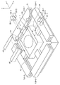
Z方向に関しても、レーザ干渉計で計測する手段が提案されている。図2は、Z方向の位置を検出するためのZレーザ干渉計構成の一例である。ステージに搭載された反射ミラー4Aで、レーザ光が垂直に上方へ反射される。基準となるレンズ定盤には45度の反射ミラー4Bが配置され、ここで、レーザ光は、水平に反射される。ほぼ投影光学系のレンズ中心付近に45度の反射ミラー4Cを設置し、レーザ光は垂直に上から下方へ投射される。ステージには反射ミラー4Dが配置され、レーザ光は、ここで垂直に反射され、来た経路を元に戻る。反射ミラー4Aはステージ上に構成されており、ステージX位置が移動すると、反射されるレーザ光もX方向に移動することになる。よって、45度ミラー4B,4Cは、X方向に長いバーミラータイプを用意する。これで、ステージがX方向に移動しても、ステージの同じ位置にレーザ光を当てることができる。ステージがY方向に移動したとき、反射ミラー4Aは、Xステージに搭載されているため、位置は変化せず、レーザ光の位置も変化しない。すると、ステージのY位置とレーザ光の相対位置が移動するため、ステージ上には、Y方向に伸びたバーミラータイプ4Dを構成する。これにより、Y方向にステージが移動しても、常にレーザ光がステージのミラー面に当たることになる。結果、ステージがXY平面を移動しても、常にレーザ干渉計による計測が可能となる。
As for the Z direction, means for measuring with a laser interferometer has been proposed. FIG. 2 is an example of a Z laser interferometer configuration for detecting a position in the Z direction. The laser beam is reflected vertically upward by the reflection mirror 4A mounted on the stage. A 45 °
ここで述べた構成以外に、ステージにY方向に延びた45度バーミラー4Eを、レンズ定盤にX方向に延びたバーミラー4Fを設置することで、ステージとレンズ定盤面の相対位置を計測することもできる(図3参照)。
In addition to the configuration described here, a 45
図2及び図3のどちらの構成においても、ステージの左右(L側、R側と称す)を対象に、同様の構成を施す。L側及びR側がXY全面で同時に計測できれば、その計測結果の平均を用いることでステージのZ位置をより正確に計測することが可能となり、また、差分を計測することでステージのチルトも計測可能となる。 2 and 3, the same configuration is applied to the left and right sides of the stage (referred to as the L side and the R side). If the L side and the R side can be measured simultaneously on the entire XY surface, the Z position of the stage can be measured more accurately by using the average of the measurement results, and the tilt of the stage can also be measured by measuring the difference. It becomes.
ステージがX方向に駆動されたとき、その位置決め精度は、X方向に伸びたバーミラー4B,4C,4Fの平面精度の影響を受ける。同様に、ステージがY方向に駆動されたとき、その位置決め精度は、Y方向に伸びたバーミラー4D,4Eの平面精度の影響を受ける。ステージのZ方向の位置決め精度は、先述のとおりnmオーダーの精度が要求されているが、バーミラー全面にわたり、nmの精度で加工し、組み立てることは、技術的にも困難である。 When the stage is driven in the X direction, the positioning accuracy is affected by the plane accuracy of the bar mirrors 4B, 4C, 4F extending in the X direction. Similarly, when the stage is driven in the Y direction, the positioning accuracy is affected by the plane accuracy of the bar mirrors 4D and 4E extending in the Y direction. As described above, the accuracy of positioning of the stage in the Z direction is required to be on the order of nm, but it is technically difficult to process and assemble the entire bar mirror with accuracy of nm.
特許文献1には、装置に搭載のフォーカスセンサを用いてステージのXY駆動によるZ誤差を事前に計測し、ステージを駆動させるときの目標位置に加味することで、Z方向の位置決め精度を向上させることが考案されている。ステージのXY駆動によるZ誤差は、バーミラーの加工精度による誤差であり、以下の説明ではステージの走り面と呼ぶこととする。
In
この手法は、ステージに搭載されたウエハ、又は、ウエハに代わる反射平面の上を、フォーカスセンサを用いて計測するものである。このとき、計測は、ウエハの表面形状の影響を受けるが、複数のフォーカスセンサを用いることでウエハの表面形状の影響を除去し、ステージの走り面の誤差だけを計測する。図5において、ウエハ上のある計測点Pを、フォーカスセンサ6Aで計測し、ステージを駆動させることで、ウエハ上の同じ計測点Pを、別のフォーカスセンサ6Bで計測する。ウエハの形状がどうであれ、同じ計測点Pを計測しているため、フォーカスセンサ6Aと6Bは同じ計測値であるはずである。ここで、同じ計測値にならないのは、ステージの駆動によってZ方向に誤差を持ったためであり、すなわち、バーミラーの加工精度の影響を受けたためである。よって、ウエハ表面の形状の影響を受けずに、バーミラーの形状を計測することができる。
In this method, a wafer mounted on a stage or a reflection plane in place of the wafer is measured using a focus sensor. At this time, the measurement is affected by the surface shape of the wafer, but the influence of the surface shape of the wafer is removed by using a plurality of focus sensors, and only the error of the stage running surface is measured. In FIG. 5, a measurement point P on the wafer is measured by the
以上で求められたZバーミラーの形状は、ステージ制御用のプロセッサー(図示せず)のメモリー上に保存される。実際の露光のシーケンスでステージを駆動させたいとき、その目標位置からZバーミラーの補正値を算出して、Z方向の位置を補正することが可能となる。その結果、Zバーミラーの形状が補正された理想的な位置に、ステージを位置決め可能となる。 The shape of the Z-bar mirror obtained as described above is stored on a memory of a stage control processor (not shown). When it is desired to drive the stage in an actual exposure sequence, it is possible to correct the position in the Z direction by calculating the correction value of the Z bar mirror from the target position. As a result, the stage can be positioned at an ideal position where the shape of the Z-bar mirror is corrected.
フォーカスセンサを用いたZバーミラー(ZXバーミラー、ZYバーミラーを総称する)の計測は、ウエハ等を用いることで、特殊な工具を用いること無く、装置だけで自己キャリブレーションが可能である点で優れている。Zバーミラーに限らず、XYバーミラーにおいても、装置のリセット時(原点出し時)の衝撃や、経時変化によって変形することも考えられる。よって、定期的にバーミラーの形状を計測する必要もあるため、特殊な工具が不要な点は、非常に重要である。 Measurement of Z-bar mirrors (collectively referring to ZX-bar mirrors and ZY-bar mirrors) using a focus sensor is superior in that self-calibration is possible using only a device without using a special tool by using a wafer or the like. Yes. Not only the Z-bar mirror but also the XY bar mirror may be deformed due to an impact at the time of resetting the apparatus (at the time of starting the origin) or a change with time. Therefore, since it is necessary to regularly measure the shape of the bar mirror, it is very important that no special tool is required.
Z、チルトの基準として、バーミラーを使用する以外の他の手法が図4に示すように存在する。その手法では、ステージ定盤面を基準としてXY平面をスライドするXYステージ上にZ、チルト駆動可能なステージを構成し、リニアエンコーダでXYステージ(ステージ定盤面基準)と、Z、チルトステージの距離を計測する。計測対象が、バーミラーになるのか、ステージ定盤面になるのかの違いであり、どちらにも同様に適応が可能である。以降、バーミラーを用いたZ、チルト計測手段において記述するが、ステージ定盤面を計測したい場合でも、まったく同様である。
上記のとおり、フォーカスセンサとウエハを用いることで、Zのバーミラー形状を正確に計測することができる。その結果、ステージをXY方向に駆動する際に、Z方向の誤差分をあらかじめ補正することで、Z方向への位置決め精度が向上し、露光装置のフォーカス精度を向上させることができる。 As described above, the bar mirror shape of Z can be accurately measured by using the focus sensor and the wafer. As a result, when the stage is driven in the XY directions, the error in the Z direction is corrected in advance, thereby improving the positioning accuracy in the Z direction and improving the focusing accuracy of the exposure apparatus.
しかし、バーミラー形状は、さまざまな要因で、徐々に、又は突然変形するおそれがある。例えば、バーミラーをねじ止めしている場合などは、このねじの締め付けによる応力により、経時的に徐々にバーミラーがもとの形状に戻ろうとする。これは、比較的長期間にわたり、バーミラーの形状が徐々に変形していくケースである。また、レーザ干渉計は相対位置計測系であるため、装置の電源投入時には、ステージの原点位置を確定させる必要がある。そのとき、機械的に突き当てを行い、原点位置を確定させる手段を用いることがある。この場合、ステージにそれ相応の力がかかることとなり、場合によっては、バーミラーの変形要因となりうる。 However, the bar mirror shape may be gradually or suddenly deformed due to various factors. For example, when the bar mirror is screwed, the bar mirror gradually returns to its original shape over time due to stress caused by tightening of the screw. This is a case where the shape of the bar mirror gradually changes over a relatively long period of time. Since the laser interferometer is a relative position measurement system, it is necessary to determine the origin position of the stage when the apparatus is turned on. At that time, there is a case in which means is used for mechanically abutting to determine the origin position. In this case, a corresponding force is applied to the stage, and depending on the case, it may be a deformation factor of the bar mirror.
バーミラーの固定に接着剤を用いる場合も同様で、接着面の経時変化や、機械的な突き当て時の力で、バーミラーの変形が発生しうる。 The same applies to the case where an adhesive is used for fixing the bar mirror, and the bar mirror can be deformed by a change in the adhesive surface with time or a force at the time of mechanical contact.
つまり、nm単位で見ると、機械的にバーミラーの形状を変動させないことは、非常に困難である。特許文献1記載の手法によって、Zバーミラーの形状を高精度に補正することができたとしても、徐々に、又は、突然に、Zの位置決め精度が悪化してしまう。
In other words, when viewed in nm units, it is very difficult to mechanically change the shape of the bar mirror. Even if the shape of the Z bar mirror can be corrected with high accuracy by the method described in
そこで、定期的に、上記手法により、Zバーミラーの形状を計測する必要がある。しかし、この場合でも、露光処理を止めて計測を行う必要があるため、露光装置の生産性を落としてしまう。また、バーミラーの変形の速度は、露光装置によってまちまちであるため、適切な計測時期を知るのは困難である。計測する間隔が長すぎると、バーミラーの変形が大きくなりすぎ、不良品を発生させてしまう恐れがあり、逆に計測を頻繁に行うと、露光装置の稼働率を下げ、生産性を低下させてしまう。さらに、いずれの場合も、バーミラーが突然変形したときには、対応できない。 Therefore, it is necessary to periodically measure the shape of the Z-bar mirror by the above method. However, even in this case, since it is necessary to stop the exposure process and perform measurement, the productivity of the exposure apparatus is lowered. In addition, since the deformation speed of the bar mirror varies depending on the exposure apparatus, it is difficult to know an appropriate measurement time. If the measurement interval is too long, the deformation of the bar mirror will become too large and may cause defective products. Conversely, if the measurement is performed frequently, the operation rate of the exposure system will be lowered and productivity will be reduced. End up. Furthermore, in any case, when the bar mirror suddenly deforms, it cannot cope.
本発明は、基板ステージの駆動に起因して発生する投影光学系の光軸方向における誤差を、露光処理を止めることなく計測しうる露光装置を提供することを目的とする。 An object of the present invention is to provide an exposure apparatus capable of measuring an error in the optical axis direction of a projection optical system caused by driving a substrate stage without stopping the exposure process.
本発明は、投影光学系を介してレチクルのパターンを基板に投影して前記基板を走査露光する露光装置であって、
前記基板を保持する基板ステージを、前記投影光学系の光軸方向と直交する第1方向に走査移動させ、前記光軸方向及び前記第1方向に直交する第2方向にステップ移動させる駆動機構と、
前記駆動機構が前記基板ステージを前記第1方向に走査移動させるときに、前記投影光学系の光軸方向における前記基板ステージの位置を計測する第1計測器と、
前記基板の上で前記第2方向に延びる一つの直線上に位置する複数の計測点で前記投影光学系の光軸方向における前記基板の表面位置を計測する第2計測器と、
制御器と、
を備え、
前記制御器は、前記基板ステージが前記第2方向にステップ移動する前と後との双方において、基板の少なくとも1つの同一の領域を前記第2計測器に前記複数の計測点の中の互いに異なる計測点で計測させ、当該第2計測器による計測結果に基づいて前記基板ステージの第2方向に沿った移動に伴う前記第1計測器の計測誤差を算出する、ことを特徴とする。
The present invention is an exposure apparatus that projects a reticle pattern onto a substrate via a projection optical system to scan and expose the substrate,
A drive mechanism that scans and moves a substrate stage that holds the substrate in a first direction orthogonal to the optical axis direction of the projection optical system, and step-moves the substrate stage in a second direction orthogonal to the optical axis direction and the first direction; ,
A first measuring instrument that measures the position of the substrate stage in the optical axis direction of the projection optical system when the drive mechanism scans and moves the substrate stage in the first direction;
A second measuring instrument that measures the surface position of the substrate in the optical axis direction of the projection optical system at a plurality of measurement points located on one straight line extending in the second direction on the substrate;
A controller;
With
The controller is configured so that at least one same region of the substrate is different from each other in the plurality of measurement points before and after the substrate stage is stepped in the second direction. The measurement is performed at a measurement point, and the measurement error of the first measuring instrument accompanying the movement of the substrate stage along the second direction is calculated based on the measurement result of the second measuring instrument.
本発明によれば、基板ステージの駆動に起因して発生する投影光学系の光軸方向における誤差を、露光処理を止めることなく計測しうる露光装置を提供することができる。その結果、露光装置の精度と生産性を両立させることが可能となる。 According to the present invention, it is possible to provide an exposure apparatus that can measure an error in the optical axis direction of the projection optical system caused by driving the substrate stage without stopping the exposure process. As a result, it is possible to achieve both the accuracy and productivity of the exposure apparatus.
以下、本発明に係る露光装置の実施形態を、シングルステージ構成、ツインステージ構成に分けて説明する。 Hereinafter, embodiments of the exposure apparatus according to the present invention will be described separately for a single stage configuration and a twin stage configuration.
[ツインステージ構成の露光装置]
ツインステージ構成の露光装置は、露光領域と、計測領域と、露光領域及び計測領域を移動可能な複数の基板ステージとを有し、計測領域で計測された基板をその計測結果に従って位置決めしながら露光領域で露光する。
[Twin-stage exposure system]
An exposure apparatus having a twin stage configuration has an exposure area, a measurement area, and a plurality of substrate stages that can move the exposure area and the measurement area, and performs exposure while positioning the substrate measured in the measurement area according to the measurement result. Exposure in the area.
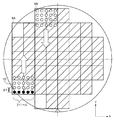
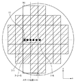
ツインステージ構成の露光装置は、図7に示されるように、計測領域のOAS位置で露光処理の前に投影光学系の光軸方向における基板(ウエハ)の表面位置(高さ位置)を計測する。基板の高さ位置(フォーカス位置)を計測する第2計測器(フォーカスセンサ)の複数の計測点7−1〜5は、X方向に延びる一つの直線上に位置する構成をとる。X方向は、投影光学系の光軸方向と直交する第1方向(Y方向)及び前記光軸方向とに直交する第2方向である。図8に示すように、基板を保持する基板ステージを図示しない駆動機構によってY方向に走査移動(スキャン)させて、フォーカスセンサを用いて複数の計測点7−1〜5で1列分の領域9Aのフォーカス計測を行う。通常、1〜数mmピッチで、Y方向にフォーカス計測点10が並ぶことになる。次に、駆動機構によって基板ステージをX方向にステップ移動させ、その後、同様に、基板ステージをY方向に走査移動させながら、隣の列の領域9Bをフォーカス計測する。これを繰り返すことで、露光が開始される前に、基板全面のフォーカス計測を事前に行っておく。
As shown in FIG. 7, the exposure apparatus with a twin stage measures the surface position (height position) of the substrate (wafer) in the optical axis direction of the projection optical system at the OAS position in the measurement area before the exposure process. . A plurality of measurement points 7-1 to -5 of the second measuring instrument (focus sensor) that measures the height position (focus position) of the substrate is configured to be positioned on one straight line extending in the X direction. The X direction is a first direction (Y direction) orthogonal to the optical axis direction of the projection optical system and a second direction orthogonal to the optical axis direction. As shown in FIG. 8, the substrate stage holding the substrate is scanned and moved in the Y direction by a drive mechanism (not shown), and a region corresponding to one row at a plurality of measurement points 7-1 to 5 using a focus sensor. 9A focus measurement is performed. Usually, the focus measurement points 10 are arranged in the Y direction at a pitch of 1 to several mm. Next, the substrate stage is moved stepwise by the drive mechanism in the X direction, and thereafter, similarly, the
このとき、通常、1列のフォーカス計測の領域は、ショットの幅と同じか、スループット向上のために複数のショットの幅を計測する場合もある。いずれの場合も、フォーカス計測範囲を計測するに十分な数のフォーカスセンサを配置する。 At this time, in general, the focus measurement area in one row may be the same as the shot width, or the width of a plurality of shots may be measured to improve throughput. In either case, a sufficient number of focus sensors are arranged to measure the focus measurement range.
このようなツインステージ構成において、本発明に係る実施形態では、図10に示されるように、1つの計測点7−6が本来の計測領域の外を計測するように、6つの計測点7−1〜6を配置する。これにより、1つの計測点7−6が隣接するフォーカス計測領域を計測することになる。本実施形態では、計測領域の外を計測する計測点の数を1つとしたが、2つ以上とすることもできる。 In such a twin stage configuration, in the embodiment according to the present invention, as shown in FIG. 10, six measurement points 7-are measured so that one measurement point 7-6 measures outside the original measurement region. 1 to 6 are arranged. As a result, the focus measurement region where one measurement point 7-6 is adjacent is measured. In the present embodiment, the number of measurement points to be measured outside the measurement region is one, but it may be two or more.
図10において9Aの領域を計測する場合、一番右の計測点7−6が、隣接する領域(図11における9B)を計測する。領域9Aを計測する場合における右端の計測点7−6の計測値を、B(X0)とする。先述の通り、Y方向は1〜数mmピッチで計測するため、B(X0)も、Y方向に複数計測される。ここでは、便宜上、基板の中心、つまり、Y=0の位置の計測値だけに注目する。後述するが、すべてのY位置のデータを平均化してしまっても、理論上、結果は同じである。(平均効果で、計測精度は向上する可能性はある。)
次に、隣接する領域9Bを計測する場合、左端の計測点7−1が、先の領域9Aを計測したときに右端の計測点7−6が計測した位置と同じ位置(図11の11)であるようにする。領域9Bを計測するときの計測点7−1の計測値をA(X1)とし、計測点7−6の計測値をB(X1)とする。
When measuring the
Next, when measuring the
同様にして、次々と隣接した領域をフォーカスセンサが6つの計測点7−1〜6でフォーカス計測することで、基板全面に亙ってフォーカス計測を行う。 Similarly, the focus sensor performs focus measurement at six measurement points 7-1 to 6 in the adjacent areas one after another, thereby performing focus measurement over the entire surface of the substrate.
ここで得られた計測値から、ZXバーミラーの形状を算出する手法は、特許文献1などで記述されている。ここでは簡単な概念だけを記述する。
A method for calculating the shape of the ZX bar mirror from the measured values obtained here is described in
n個の領域を基板ステージがX方向にステップ移動する前と後との双方において、基板の同一の領域を互いに異なる右端の計測点7−6と左端の計測点7−1とで計測することにより得られる計測結果は、以下のとおりである。ここで、B(X0〜Xn−1)は、基板ステージ位置XがX0〜Xn−1における右端の計測点7−6での計測結果である。A(X1〜Xn)は、基板ステージ位置XがX1〜Xnにおける左端の計測点7−1での計測結果である。
B(X0)
B(X1)、 A(X1)
B(X2)、 A(X2)
:
B(Xn―1)、A(Xn―1)
A(Xn)
このとき、X0〜Xnは以下の関係にある。
X1=X0+XF
X2=X1+XF=X0+2XF
:
Xn=Xn−1+XF=X0+nXF
ここで、XFは、フォーカス計測領域の幅であり、隣接する領域を計測するために、基板ステージがステップ移動する幅である。
Measure the same area of the substrate at the rightmost measurement point 7-6 and the leftmost measurement point 7-1 both before and after the substrate stage is stepped in the X direction in the n areas. The measurement results obtained by are as follows. Here, B (X0 to Xn-1) is a measurement result at the measurement point 7-6 at the right end when the substrate stage position X is X0 to Xn-1. A (X1 to Xn) is a measurement result at the measurement point 7-1 at the left end when the substrate stage position X is X1 to Xn.
B (X0)
B (X1), A (X1)
B (X2), A (X2)
:
B (Xn-1), A (Xn-1)
A (Xn)
At this time, X0 to Xn have the following relationship.
X1 = X0 + XF
X2 = X1 + XF = X0 + 2XF
:
Xn = Xn-1 + XF = X0 + nXF
Here, XF is the width of the focus measurement area, and is the width by which the substrate stage moves stepwise in order to measure adjacent areas.
B(X0)とA(X1)は、基板上の同じ位置11の計測結果である。つまり、ステージ走りが理想的平坦であれば、同じ値を示すはずである。つまり、この2つの計測結果の差が、ステージの走りが理想面からずれた量、すなわち、ZXバーミラーの形状の影響をうけたものである。この量を、基板ステージがX0→X1に駆動したときの、Z誤差ΔZとして、下記のように定義する。
ΔZ(X0→X1)=A(X1)−B(X0)
ΔZ(X1→X2)=A(X2)−B(X1)
:
ΔZ(Xn−1→Xn)=A(Xn)−B(Xn−1)
上記式は、基板ステージが、XFだけ駆動したときの、誤差の差分を示している。これを、ZXのバーミラーの絶対値Z(X0〜Xn)に変換するためには、上記を累積していけばよい。このとき、絶対値の基準がないため、とりあえず、基板ステージがX0のときにおけるバーミラーの誤差成分を0と仮定する。
Z(X0)=0
Z(X1)=Z(X0)+ΔZ(X0→X1)=0+ΔZ(X0→X1)
Z(X2)=Z(X1)+ΔZ(X1→X2)=0+ΔZ(X0→X1)+ΔZ(X1→X2)
:
Z(Xn)=Z(Xn−1)+ΔZ(Xn−1→Xn)=ΔZ(X0→X1)+・・・+ΔZ(Xn−1→Xn)
ここで、X=X0を、ZXバーミラーの形状を判断する基準としたが、これは、計算の便宜上であり、どこを基準としても問題はない。たとえば、X=Xcを、ZXバーミラーの形状を判断する基準としたい場合、全配列から、Z(Xc)の値を引いてやればよい。その場合には、以下のようになる。
Z(X0)→Z(X0)―Z(Xc)
Z(X1)→Z(X1)―Z(Xc)
:
Z(Xc)→Z(Xc)―Z(Xc)=0
:
Z(Xn)→Z(Xn)―Z(Xc)
ここで得られるZXバーミラーの形状は、あくまで、前回、計測・補正してからの変化量である。つまり、ZXバーミラーが変化していなければ、上記関数Z(X)は、0か、計測誤差程度のごく小さい値となる。
B (X0) and A (X1) are measurement results at the
ΔZ (X0 → X1) = A (X1) −B (X0)
ΔZ (X1 → X2) = A (X2) −B (X1)
:
ΔZ (Xn−1 → Xn) = A (Xn) −B (Xn−1)
The above equation shows the difference in error when the substrate stage is driven by XF. In order to convert this into the absolute value Z (X0 to Xn) of the ZX bar mirror, the above may be accumulated. At this time, since there is no absolute value reference, it is assumed that the error component of the bar mirror when the substrate stage is X0 is zero.
Z (X0) = 0
Z (X1) = Z (X0) + ΔZ (X0 → X1) = 0 + ΔZ (X0 → X1)
Z (X2) = Z (X1) + ΔZ (X1 → X2) = 0 + ΔZ (X0 → X1) + ΔZ (X1 → X2)
:
Z (Xn) = Z (Xn−1) + ΔZ (Xn−1 → Xn) = ΔZ (X0 → X1) +... + ΔZ (Xn−1 → Xn)
Here, X = X0 is used as a reference for determining the shape of the ZX bar mirror, but this is for convenience of calculation, and there is no problem regardless of the reference. For example, when X = Xc is desired as a reference for determining the shape of the ZX bar mirror, the value of Z (Xc) may be subtracted from the entire array. In that case, it becomes as follows.
Z (X0) → Z (X0) −Z (Xc)
Z (X1) → Z (X1) −Z (Xc)
:
Z (Xc) → Z (Xc) −Z (Xc) = 0
:
Z (Xn) → Z (Xn) −Z (Xc)
The shape of the ZX bar mirror obtained here is the amount of change since the last measurement / correction. That is, if the ZX bar mirror is not changed, the function Z (X) is 0 or a very small value such as a measurement error.
ここで、閾値をあらかじめ設定しておき、Z(X)が、閾値を超えたら、改めて、ZXバーミラーを精密に計測する時期を決定するように設けうる。この手法は、例えば、特許文献1に示されている。
Here, a threshold value may be set in advance, and when Z (X) exceeds the threshold value, it may be provided so as to determine the timing for precisely measuring the ZX bar mirror. This technique is disclosed in
もちろん、ここで求められたZ(X)のデータを、ZXバーミラーの補正関数に加算することも可能である。このとき、同一の点を重複して計測するセンサが1つでなく複数であれば、ステージがX駆動したときのZ誤差のみでなく、チルトの誤差も計測することが可能である。 Of course, it is also possible to add the Z (X) data obtained here to the correction function of the ZX bar mirror. At this time, if there are a plurality of sensors for measuring the same point in duplicate, it is possible to measure not only the Z error when the stage is driven in X but also the tilt error.
以上のように、本来のフォーカス計測領域における計測点の数より多く計測点を設けることで、ZXバーミラーの形状の変動を計測することが可能である。 As described above, it is possible to measure the variation in the shape of the ZX bar mirror by providing more measurement points than the number of measurement points in the original focus measurement region.
ここで、ZXバーミラーは、干渉計とともに、基板ステージが走査移動するときに基板ステージの高さ位置を計測する第1計測器を構成している。また、上述したZXバーミラー及び干渉計に起因する計測誤差を不図示の制御器が算出する。 Here, the ZX bar mirror, together with the interferometer, constitutes a first measuring instrument that measures the height position of the substrate stage when the substrate stage scans and moves. Further, a controller (not shown) calculates a measurement error caused by the ZX bar mirror and the interferometer described above.
上記のような計測手法が成立するのは、X方向へのステップサイズXFと、計測点7−1と7−6との距離が一致している場合のみである。X方向へのステップサイズは、フォーカス計測領域のX方向のサイズと同じであり、つまり、ショットサイズの整数倍(複数ショット同時計測の場合、図8の場合は、2ショットの幅)である。よって、ショットサイズによっては、2つの計測点での基板の表面位置がぴったりとは重ならない。 The measurement method as described above is established only when the step size XF in the X direction and the distance between the measurement points 7-1 and 7-6 match. The step size in the X direction is the same as the size in the X direction of the focus measurement region, that is, an integral multiple of the shot size (in the case of simultaneous measurement of multiple shots, the width of two shots in the case of FIG. 8). Therefore, depending on the shot size, the surface positions of the substrates at the two measurement points do not exactly overlap.
基板の表面が、十分に平坦であれば、必ずしも、2つの計測点での基板表面位置がぴったりとは一致しなくても、基板表面位置が互いに近接していたら誤差は大きくない。つまり、各計測点の間隔を、十分に小さくしておけば、すなわち、フォーカス計測領域内に多くの計測点が存在するように設けておけば、十分に実用に耐えることが可能となる。 If the surface of the substrate is sufficiently flat, even if the substrate surface positions at the two measurement points are not exactly the same, the error is not large if the substrate surface positions are close to each other. That is, if the interval between the measurement points is sufficiently small, that is, if the measurement points are provided so that there are many measurement points in the focus measurement region, it is possible to sufficiently withstand practical use.
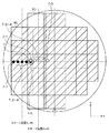
この場合、もちろん、コストなどの問題もあるため、必ずしも、計測点を多く配置できるとは限らない。しかしながら、図8のような、通常のフォーカス計測を行う領域にしか、計測点が配置されていない構成においても、本発明は適用可能である。すなわち、図10のように、本来のフォーカス計測領域の計測点より多く計測点を設けるのでなく、ZXバーミラーを計測したい時だけ、フォーカス計測領域を小さくすればよい。 In this case, of course, there are also problems such as cost, and it is not always possible to arrange many measurement points. However, the present invention can also be applied to a configuration in which measurement points are arranged only in a region where normal focus measurement is performed as shown in FIG. That is, as shown in FIG. 10, it is only necessary to reduce the focus measurement area only when it is desired to measure the ZX bar mirror, instead of providing more measurement points than the original focus measurement area.
この態様を図12に示す。ここで、本来のフォーカス計測は2列同時に行われる。フォーカスセンサの計測点は、2ショット分の幅の内側にしか構成されていない。本来のフォーカス計測領域の幅は、2ショット分の幅と同じになるように設定するが、フォーカスセンサを用いてステージ走りによる誤差を算出するモードにおいては、フォーカス計測領域9Cを2ショット分の幅より小さくする。すると、フォーカスセンサの右端の計測点7−5は、フォーカス計測領域9Cの外に位置することになる。続いて、基板ステージをX方向にステップ駆動して、同様に、フォーカス計測領域9Dを計測する。このとき、左端の計測点7−1が、右端の計測点7−5で先に計測した同じ基板表面位置11を計測する。このように、ステージ走りによる計測誤差を算出するモードにおけるフォーカス計測領域を、ショットの幅(の2倍)より小さくすることで、同様の効果を得ることができる。
This aspect is shown in FIG. Here, the original focus measurement is performed simultaneously for two rows. The measurement point of the focus sensor is configured only inside the width for two shots. The width of the original focus measurement area is set to be the same as the width of two shots. However, in the mode for calculating an error due to the stage running using the focus sensor, the
このとき、フォーカス計測領域が、X方向に小さくなってしまうため、基板全面を計測するためには、より多くの領域を計測しなければならない。つまり、計測時間は増加してしまう。 At this time, since the focus measurement area becomes smaller in the X direction, more areas must be measured in order to measure the entire surface of the substrate. That is, the measurement time increases.
また、すでに露光済みの基板を重ね焼きする場合(下地がある場合)、下地のパターンによる、フォーカスセンサのだまされ(誤差)成分を、除去する必要がある。通常は、基板全面において、全ショットの共通成分、つまり、全ショットの平均値を、計測値から引いてやる必要がある。X方向のステップサイズXFが、ショットの整数倍の場合、フォーカスセンサは、各計測点でショット内の同じ場所を計測するため、先の手段により、基板全体におけるショット共通成分を除去することは、容易である。しかし、フォーカス計測領域9Cを2ショット分の幅より小さくするような場合では、フォーカス計測領域毎に、各計測点でのショット内の基板表面位置が異なってしまう。
Further, when an already exposed substrate is overprinted (when there is a ground), it is necessary to remove the deceiving (error) component of the focus sensor due to the ground pattern. Usually, it is necessary to subtract the common component of all shots, that is, the average value of all shots, from the measured value over the entire surface of the substrate. When the step size XF in the X direction is an integral multiple of the shot, the focus sensor measures the same location in the shot at each measurement point. Easy. However, when the
そこで、このような場合には、下地のパターンを有さない基板に露光する場合に限るなど、条件を設けてもよい。下地のパターンがなければ、パターンによるだまされも生じないため、上記問題は発生しない。また、下地のパターンがない基板については、下地のショットの位置を正確に計測するアライメント計測が不要であるため、そもそも、計測ステーション側は、時間的に余裕がある。よって、下地のパターンがない基板だけについて、Zバーミラーの計測を行うことで、スループットの低下もおさえることができる。 Therefore, in such a case, conditions may be set such that the exposure is performed only on a substrate having no underlying pattern. If there is no underlying pattern, the above-described problem does not occur because the pattern is not fooled. In addition, for a substrate without a base pattern, alignment measurement for accurately measuring the position of the base shot is unnecessary, so that the measurement station side has some time in the first place. Therefore, the throughput can be reduced by measuring the Z-bar mirror only for the substrate having no underlying pattern.
通常、バーミラーの変形は、ゆるやかであるため、必ずしも、毎回、Z方向の誤差を計測する必要はない。ある一定期間ごとでも十分である。よって、下地のパターンがない基板にだけ、Z方向の誤差を計測しても十分である。例えば、予め定められた枚数の基板が処理される毎に計測することとしうる。基板処理枚数の代わりに、予め定められた時間が経過する毎に計測するように設けてもよい。また、露光装置の電源を投入した直後は、バーミラーの形状が突然変形している可能性もあるため、電源を投入したときに、Z方向の誤差を計測することが望ましい。 Usually, since the deformation of the bar mirror is gentle, it is not always necessary to measure the error in the Z direction every time. Even a certain period is sufficient. Therefore, it is sufficient to measure an error in the Z direction only for a substrate having no underlying pattern. For example, it may be measured each time a predetermined number of substrates are processed. Instead of the number of processed substrates, a measurement may be provided every time a predetermined time elapses. Further, since the shape of the bar mirror may be suddenly deformed immediately after the exposure apparatus is turned on, it is desirable to measure an error in the Z direction when the power is turned on.
下地のパターンがある基板において、ZXバーミラーを計測したい時だけフォーカス計測領域を小さくする場合、ショット共通成分を基板全面で取り除くのではなく、ショット共通成分をフォーカス領域毎に取り除きうる。すなわち、図12において、ショットの共通成分を領域9Cにて除去する。通常、Y方向に並んだショットでは、フォーカスセンサが、各計測点で同じ基板表面位置を計測するので、この単位、つまり、Y方向に並んだショットの単位で、ショットに共通の成分を除去すればよい。領域9Cでは、ショットが2列あるので、同様な処理を2回行うことになる。同様に、領域9Dにおいても、Y方向に並んだショット共通成分を除去する。少しでも計測を行ったショットに関して行うので、領域9Dでは、3回行うことになる。これを、基板全面において、繰り返すことで、パターンによるだまされを除去することが可能となる。この結果、本来のフォーカス計測領域の計測点より計測点が多く設置される場合、XステップサイズXFがショットのX幅の整数倍でない場合も、下地のだまされを除去しながら、Zバーミラーの誤差の計測が可能である。ただし、図10のように、基板全面で共通の成分を算出した方が、精度は良くなる。
When the focus measurement region is reduced only when it is desired to measure the ZX bar mirror on the substrate having the base pattern, the shot common component can be removed for each focus region instead of removing the shot common component over the entire surface of the substrate. That is, in FIG. 12, the common component of the shot is removed in the
以上、ZXバーミラーの誤差の計測方法について述べた。ZXバーミラーによる誤差は、基板ステージがX方向に駆動したときのZ誤差である。ここでは、各フォーカス計測領域において、Y=0のみに注目したが、すべてのY位置において、B(X0)とA(X1)の差は同じである。よって、すべてのY位置において、平均化してしまっても、同様にZXバーミラーの形状を計測可能であり、かつ、平均化効果により、計測誤差を低減させることが可能となる。 The method for measuring the error of the ZX bar mirror has been described above. The error due to the ZX bar mirror is a Z error when the substrate stage is driven in the X direction. Here, attention is paid only to Y = 0 in each focus measurement region, but the difference between B (X0) and A (X1) is the same at all Y positions. Therefore, even if averaging is performed at all the Y positions, the shape of the ZX bar mirror can be measured similarly, and the measurement error can be reduced due to the averaging effect.
以上、ZXバーミラーについて述べた。しかし、ZYバーミラーについても、図13のように、Y方向に基板ステージを駆動したときに重なるよう、Y方向にシフトさせた計測点8を配置することで、誤差を計測可能である。 The ZX bar mirror has been described above. However, with respect to the ZY bar mirror, as shown in FIG. 13, the error can be measured by arranging the measurement points 8 shifted in the Y direction so as to overlap when the substrate stage is driven in the Y direction.
Y方向への計測ピッチは、自由に設定できるため、計測点が必ず重なるようにすることは容易である。Y方向へずらして配置されたセンサ位置がYLだけ離れたとすれば、基板全面をフォーカス計測する際の計測ピッチを、YLと同じ、又は、YLの整数分の1とすればよい。そうすれば、複数のY方向にシフトさせた計測点と同じ基板表面位置を、異なる計測点での基板表面位置と重ねること可能となる。以下は、X方向と同様な原理で、ZYのバーミラーの形状を算出可能である。よって、以下の説明は割愛する。 Since the measurement pitch in the Y direction can be set freely, it is easy to ensure that the measurement points overlap. If the sensor position shifted in the Y direction is separated by YL, the measurement pitch when the focus measurement is performed on the entire surface of the substrate may be the same as YL or 1 / integer of YL. If it does so, it becomes possible to overlap the same substrate surface position as the measurement point shifted in the several Y direction with the substrate surface position in a different measurement point. In the following, the shape of the ZY bar mirror can be calculated on the same principle as in the X direction. Therefore, the following description is omitted.
[シングルステージ構成の露光装置]
次に、シングルステージ構成の露光装置で用いられる、露光直前にフォーカス計測する場合について、説明する。
[Single-stage exposure system]
Next, a case where focus measurement is performed immediately before exposure used in an exposure apparatus having a single stage configuration will be described.
露光直前にフォーカス計測を行う手法は、静止露光方式とスキャン露光方式とで異なる。ここでは、近年主流のスキャン露光方式について述べる。 The method of performing focus measurement immediately before exposure differs between the static exposure method and the scan exposure method. Here, a description will be given of a scan exposure system which has been mainly used in recent years.
スキャン露光方式のステージ構成及びフォーカスセンサの配置を図6に示す。露光光は、露光スリットを通り、矩形の露光形状を形成する。基板ステージを駆動させることによって、矩形の露光範囲が基板上を移動し、1ショット分、露光を行う。よって、1ショットの露光領域の大きいことが特徴である。 FIG. 6 shows the scanning exposure stage configuration and the arrangement of the focus sensors. The exposure light passes through the exposure slit and forms a rectangular exposure shape. By driving the substrate stage, the rectangular exposure range moves on the substrate, and exposure is performed for one shot. Therefore, the exposure area of one shot is large.
露光スリット長手方向を第1の方向(X方向)とし、露光スリット短手方向を第2の方向(Y方向)とする。基板ステージは、露光しながらY方向に走査移動(スキャン)し、隣接したショットを露光するためにX方向へステップ移動することとなる。 The longitudinal direction of the exposure slit is the first direction (X direction), and the short direction of the exposure slit is the second direction (Y direction). The substrate stage is scanned and moved in the Y direction while being exposed, and is moved stepwise in the X direction to expose adjacent shots.
フォーカスセンサ6A,6Cは、通常、露光スリットの数mm手前に配置されており、露光スリットが露光領域に入る事前にフォーカス計測を行う。露光スリットが露光領域に入るまでに、基板ステージをZ方向に駆動することで、ベストなフォーカスで露光を行うことが可能となる。このフォーカスセンサの計測点を、X方向やY方向に複数設けることで、露光スリットにおけるチルトも計測可能となる。図では、便宜上、X方向のみに配置した例を図示している。
The
このようなステージ構成における具体的な方式を、以下に述べる。 A specific method in such a stage configuration will be described below.
従来のフォーカスセンサは、最大露光幅(X方向の幅)より小さい領域内のZ方向位置及びチルトを計測する。しかし、本実施形態では、図9のように、最大露光領域よりを超える範囲にも、計測点が存在するように設ける。 The conventional focus sensor measures the Z-direction position and tilt in an area smaller than the maximum exposure width (X-direction width). However, in the present embodiment, as shown in FIG. 9, the measurement points are provided in a range exceeding the maximum exposure area.
図14に沿って説明する。基板ステージが第1露光領域12−1を走査移動させて露光する場合、露光スリットが露光領域に到達する前に、計測点6A−1〜3で基板上の高さを計測する。露光スリットが露光領域に到達したときには、基板ステージのZ方向及びチルトの駆動が終了している。このとき、ステージが追い込まれたかどうかを確認するために、スリット位置を計測するフォーカスセンサを用いて計測点6B−1〜3で計測を行う。ここまでは、通常の露光シーケンスでも行われる。しかし、本実施形態では、余分に配置された右端の計測点6B−4で、露光領域の外側の隣接する露光領域12−2を計測することになる。第1露光領域12−1の露光終了後、基板ステージをX方向にステップ移動させて隣接した第2露光領域12−2を露光する場合、左端の計測点6B−1で、第1露光領域12−1の露光時に右端の計測点6B−4で計測した同じ基板表面位置13を計測する。
A description will be given along FIG. When the substrate stage performs exposure by scanning and moving the first exposure region 12-1, the height on the substrate is measured at the measurement points 6A-1 to 3A-3 before the exposure slit reaches the exposure region. When the exposure slit reaches the exposure area, driving of the substrate stage in the Z direction and tilt is completed. At this time, in order to confirm whether or not the stage has been driven, measurement is performed at
以降は、ツインステージの時と同様である。すなわち、基板上の同じ位置を計測しているため、同じ計測値であるはずである。これが異なる計測値となるのは、基板ステージがX駆動によって、Z方向への誤差が生じているためである。その原因は、Zバーミラーの経時変化であり、調整が必要であることを示している。この計測を基板全面について行うことで、基板ステージ駆動範囲におけるZバーミラーの形状を算出することが可能である。 The subsequent steps are the same as in the twin stage. That is, since the same position on the substrate is measured, the measured values should be the same. The reason why this is a different measurement value is that an error in the Z direction occurs due to the X drive of the substrate stage. The cause is a change with time of the Z-bar mirror, indicating that adjustment is necessary. By performing this measurement on the entire surface of the substrate, the shape of the Z bar mirror in the substrate stage driving range can be calculated.
ツインステージ構成の場合、通常、基板のZ方向及びチルトは、一定の状態で、隣接した領域を計測する。それに対し、シングルステージ構成、つまり、リアルタイムフォーカスの場合、露光領域ごとに基板ステージのZ方向及びチルトを駆動している。そのため、フォーカスセンサの計測値だけでなく、基板ステージの駆動量も計算に含める必要がある。単純化のため、Z方向にのみ基板ステージを駆動した場合を考える。ツインステージ構成の場合と同様、ステージX位置における、計測点6B−4での計測結果をB(X)、計測点6B−1での計測結果をA(X)とし、基板ステージのZ駆動量をS(X)とすると、それらは以下のようになる。
B(X0)、 S(X0)
B(X1)、 A(X1)、 S(X1)
B(X2)、 A(X2)、 S(X2)
:
B(Xn−1)、A(Xn−1)、S(Xn−1)
A(Xn)、 S(Xn)
Z誤差ΔZは基板ステージの駆動量を考慮して以下のようになる。
ΔZ(X0→X1)={A(X1)−S(X1)}−{B(X0)−S(X0)}
ΔZ(X1→X2)={A(X2)−S(X2)}−{B(X1)−S(X1)}
:
ΔZ(Xn−1→Xn)={A(Xn)−S(Xn)}−{B(Xn−1)−S(Xn−1)}
シングルステージ構成においても、ツインステージ構成と全く同様に、基板全面におけるZバーミラーの形状を算出することができる。
In the case of a twin stage configuration, usually, adjacent regions are measured while the Z direction and tilt of the substrate are constant. On the other hand, in the case of a single stage configuration, that is, real-time focus, the Z direction and tilt of the substrate stage are driven for each exposure region. Therefore, it is necessary to include not only the measurement value of the focus sensor but also the driving amount of the substrate stage in the calculation. For simplicity, consider the case where the substrate stage is driven only in the Z direction. As in the case of the twin stage configuration, the measurement result at the
B (X0), S (X0)
B (X1), A (X1), S (X1)
B (X2), A (X2), S (X2)
:
B (Xn-1), A (Xn-1), S (Xn-1)
A (Xn), S (Xn)
The Z error ΔZ is as follows in consideration of the driving amount of the substrate stage.
ΔZ (X0 → X1) = {A (X1) −S (X1)} − {B (X0) −S (X0)}
ΔZ (X1 → X2) = {A (X2) −S (X2)} − {B (X1) −S (X1)}
:
ΔZ (Xn−1 → Xn) = {A (Xn) −S (Xn)} − {B (Xn−1) −S (Xn−1)}
In the single stage configuration, the shape of the Z-bar mirror on the entire surface of the substrate can be calculated just like the twin stage configuration.
チルト駆動を伴う場合、回転中心からの距離とチルト量からフォーカス計測位置におけるZ量に変換すれば、上記と同様に計算できる。 When tilt drive is involved, the calculation can be performed in the same manner as described above by converting the distance from the rotation center and the tilt amount into the Z amount at the focus measurement position.
ステージ位置XにおけるZ方向の駆動量をZs(X)、X方向への傾きをTilt−X(X)、回転中心からフォーカス計測位置までの距離をXrot(X)、Y方向への傾きをTilt−Y(X)とする。また、回転中心からフォーカス計測位置までの距離をYrot(X)とすると、以下の関係が成り立つ。
S(X)=Zs(X)+Tilt−X(X)・Xrot(X)+Tilt−Y(X)・Yrot(X)
各X位置(X0,X1,・・・Xn)において、上記式を適応すればよい。
The drive amount in the Z direction at the stage position X is Zs (X), the tilt in the X direction is Tilt-X (X), the distance from the rotation center to the focus measurement position is Xrot (X), and the tilt in the Y direction is Tilt. -Y (X). Further, if the distance from the rotation center to the focus measurement position is Yrot (X), the following relationship is established.
S (X) = Zs (X) + Tilt-X (X) .Xrot (X) + Tilt-Y (X) .Yrot (X)
The above equation may be applied to each X position (X0, X1,... Xn).
ここで、フォーカス計測位置から回転中心までの距離は、各X位置において可変としているが、ステージの制御方式によっては、固定値になる場合もある。また、回転角について、どちらの方向を正方向(+)とするかによって、上記式の符号も反転し、加算部分が減算になる。ここでは、詳細には触れない。 Here, the distance from the focus measurement position to the center of rotation is variable at each X position, but may be a fixed value depending on the stage control method. Further, the sign of the above formula is inverted depending on which direction is the positive direction (+) with respect to the rotation angle, and the addition portion is subtracted. I won't go into details here.
上記は、便宜上、Y=0の位置のみで記述しているが、通常、1つの露光領域内に数mm間隔で複数の計測位置がY方向に並んでいる。これらをすべて平均化してもよい。また、露光領域も、Y方向に複数並んでいるので、さらに平均化することで、計測誤差の影響を減少させることが可能となる。 The above is described only with the position of Y = 0 for convenience, but normally, a plurality of measurement positions are arranged in the Y direction at intervals of several mm within one exposure region. All of these may be averaged. In addition, since a plurality of exposure regions are arranged in the Y direction, the influence of measurement errors can be reduced by further averaging.
また、上記式は、中心に配置されるフォーカスセンサの計測点6B−1と6B−4とを重ね合わせることを前提に記述しているが、先読みセンサの計測点6A−1と6A−4、又は、6C−1と6C−4を重ね合わせても、同様な効果を得ることができる。よって、これらのどれか1つの組合せを使用してもよいし、すべての組合せの平均を用いてもよい。 In addition, the above formula is described on the assumption that measurement points 6B-1 and 6B-4 of the focus sensor arranged at the center are overlapped, but measurement points 6A-1 and 6A-4 of the pre-reading sensor, Or even if 6C-1 and 6C-4 are overlapped, the same effect can be obtained. Therefore, any one of these combinations may be used, or an average of all the combinations may be used.
図14は、フォーカスセンサの計測点を、片側だけに1つ多く配置した例を記載している。しかし、露光領域の両側に1つづつ多く配置したり、複数多く配置したりすると、X駆動におけるZ方向の誤差のみでなく、Tiltの誤差も計測しうる。ただし、多くの計測点を配置すれば、コストももちろん高くなる。 FIG. 14 shows an example in which one focus sensor measurement point is arranged on only one side. However, if one is arranged on each side of the exposure area, or a plurality is arranged, not only errors in the Z direction in X driving but also Tilt errors can be measured. However, if many measurement points are arranged, the cost will naturally increase.
上記式が成立する場合は、計測点6B−1と6B−4で計測される基板表面位置が完全に重なる、つまり、6B−1と6B−4の間隔と、露光領域(ショット)の幅(X方向へのステップ駆動量)とが同じ場合である。しかし、通常の露光においては、露光領域の幅は、露光するパターンによってさまざまである。そこで、フォーカスセンサの計測点6B−1と6B−4で基板上の同じ位置を計測しなくても、ごく近傍を計測したときも、同様なことを行っても良い。とくに、下地に露光済みのパターンがない場合で、基板の平坦度が十分に良ければ、十分に計測は可能である。 If the above equation holds, the substrate surface positions measured at the measurement points 6B-1 and 6B-4 are completely overlapped, that is, the interval between 6B-1 and 6B-4 and the width of the exposure region (shot) ( The step drive amount in the X direction) is the same. However, in normal exposure, the width of the exposure area varies depending on the pattern to be exposed. Therefore, the same thing may be performed when measuring the very vicinity without measuring the same position on the substrate at the measurement points 6B-1 and 6B-4 of the focus sensor. In particular, if there is no exposed pattern on the base and the substrate has sufficiently good flatness, sufficient measurement is possible.
また、図14は、露光領域内に3つの計測点6B−1〜3、露光領域外に1つの計測点6B−4を配置した図を記載している。これらの計測点間の間隔を小さくし、より多くの計測点を配置することで、いかなるショットの幅でも、2つ以上の計測点で基板上の同じ(又はごく近傍)の位置を計測することが可能となる。
FIG. 14 shows a diagram in which three
先述の通り、通常の露光シーケンスにおいて、ショットの幅は様々であり、常に、最大露光幅で露光を行うとは限らない。露光領域の幅(X方向)が、フォーカスセンサの幅よりも小さい場合に、シングルステージ構成のリアルタイムフォーカスにおいてもZ方向の誤差成分を算出し得る。例えば、露光装置の電源を投入したとき、あるいは基板ステージの原点位置を決定するとき、又は露光処理を行うロットの最初の基板に対してZ方向の誤差成分を算出し得る。この場合、最大露光幅より多くの計測点を配置する必要がない。すなわち、図14でいう、計測点6B−4が不要であるため、コスト的にも有利である。およそすべての露光装置において、実施可能である。ただし、すべての露光において、本発明に係るフォーカス計測手法が可能ではなく、あくまで、フォーカスセンサの幅より小さいショットを露光するときに限定される。以下は、同様であるため、割愛する。
As described above, in the normal exposure sequence, the shot width varies, and the exposure is not always performed with the maximum exposure width. When the width of the exposure region (X direction) is smaller than the width of the focus sensor, an error component in the Z direction can be calculated even in real-time focusing with a single stage configuration. For example, the error component in the Z direction can be calculated when the exposure apparatus is turned on, when the origin position of the substrate stage is determined, or with respect to the first substrate of the lot for which the exposure process is performed. In this case, it is not necessary to arrange more measurement points than the maximum exposure width. That is, since the
X方向のZバーミラーに関しては、上記の手法で調整可能である。Y方向に関しては、通常、先読みセンサが配置されているので、改めて計測点を配置する必要はない。通常の露光シーケンス中に、同じ位置を別の計測点で計測することでZ方向の誤差成分を算出し得る。すなわち、事前にフォーカスセンサ6A−1〜3で計測した基板上の位置を、Y方向にスキャンした後、フォーカスセンサ6B−1〜3で計測すれば、同様の手段を用いることが可能となる。
The Z bar mirror in the X direction can be adjusted by the above method. Regarding the Y direction, since the pre-reading sensor is usually arranged, there is no need to arrange measurement points again. An error component in the Z direction can be calculated by measuring the same position at different measurement points during a normal exposure sequence. That is, if the position on the substrate measured in advance by the
なお、静止露光の場合は、スキャン露光装置のX方向の場合と、同等のことがいえる。すなわち、最大露光幅よりXY方向に広い範囲に計測点を配置したり、また、計測点の範囲よりX又はY方向に小さい領域を露光したりすればよい。 In the case of still exposure, the same can be said as in the X direction of the scan exposure apparatus. That is, the measurement points may be arranged in a range wider than the maximum exposure width in the XY direction, or an area smaller than the measurement point range in the X or Y direction may be exposed.
上記手法により、Zのバーミラーの形状が算出された後の処理は、ツインステージの場合と、まったく同様である。閾値をあらかじめ設定しておき、Z(X)が閾値を超えたら、改めてZXバーミラーの計測を行ってもよい。ここで求められたZ(X)のデータを、ZXバーミラーの補正関数に加算してもよい。 The processing after the Z bar mirror shape is calculated by the above method is exactly the same as in the case of the twin stage. A threshold value is set in advance, and when Z (X) exceeds the threshold value, the ZX bar mirror may be measured again. The Z (X) data obtained here may be added to the correction function of the ZX bar mirror.
計測時期もショット毎に行ってもよいし、下地のパターンを有さない基板に対してだけ本提案の計測手法を用いてもよい。予め設定された枚数の基板が処理される毎に、本発明の計測手法を行ってもよいし、予め設定された時間が経過する毎に本発明の手法を行ってもよい。また、電源を投入した直後には、本発明による計測手法を必ず行うとしてもよい。 The measurement timing may be performed for each shot, or the proposed measurement method may be used only for a substrate having no underlying pattern. The measurement method of the present invention may be performed every time a predetermined number of substrates are processed, or the method of the present invention may be performed every time a preset time elapses. Also, immediately after the power is turned on, the measurement method according to the present invention may be performed without fail.
[露光装置の説明]
本発明で適用される例示的なシングルステージ構成の露光装置を説明する。露光装置は図15に示すように、照明装置101、レチクルを搭載したレチクルステージ102、投影光学系103、基板を保持する基板ステージ1とを備える。上述したように基板ステージ1は、不図示の駆動機構によってY方向に操作移動され、X方向にステップ移動される。露光装置は、レチクルに形成された回路パターンを基板に投影して走査露光する。
[Explanation of exposure apparatus]
An exemplary single-stage exposure apparatus applied in the present invention will be described. As shown in FIG. 15, the exposure apparatus includes an
照明装置101は回路パターンが形成されたレチクルを照明し、光源部と照明光学系とを有する。光源部は、例えば、光源としてレーザを使用する。レーザは、波長約193nmのArFエキシマレーザ、波長約248nmのKrFエキシマレーザ、波長約153nmのF2エキシマレーザなどを使用することができる。しかし、レーザの種類はエキシマレーザに限定されず、例えば、YAGレーザを使用してもよいし、そのレーザの個数も限定されない。光源にレーザが使用される場合、レーザ光源からの平行光束を所望のビーム形状に整形する光束整形光学系、コヒーレントなレーザ光束をインコヒーレント化するインコヒーレント化光学系を使用することが好ましい。また、光源部に使用可能な光源はレーザに限定されるものではなく、一又は複数の水銀ランプやキセノンランプなどのランプも使用可能である。照明光学系はマスクを照明する光学系であり、レンズ、ミラー、ライトインテグレーター、絞り等を含む。
The
投影光学系103は、複数のレンズ素子のみからなる光学系、複数のレンズ素子と少なくとも一枚の凹面鏡とを有する光学系、複数のレンズ素子と少なくとも一枚のキノフォーム等の回折光学素子とを有する光学系、全ミラー型の光学系等を使用することができる。
The projection
レチクルステージ102及び基板ステージ1は、例えばリニアモータによって移動可能である。それぞれのステージは同期して移動する。また、レチクルのパターンを基板上に位置合わせするために基板ステージ1及びレチクルステージ102に不図示のアクチュエータ(駆動機構)を備える。
The
図15に示されるような露光装置を用いて基板を露光する工程の後、露光された基板を現像する工程等を経て、半導体集積回路等の半導体デバイスや、マイクロマシン、薄膜磁気ヘッド等の微細なパターンが形成されたデバイスが製造されうる。 After the step of exposing the substrate using the exposure apparatus as shown in FIG. 15, the step of developing the exposed substrate, etc., is followed by the steps of developing semiconductor devices such as semiconductor integrated circuits, micromachines, thin film magnetic heads, etc. A device in which a pattern is formed can be manufactured.
1:基板ステージ
2A:Xバーミラー
2B:Yバーミラー
3A−1:Xレーザ干渉計
3A−2:チルトレーザ干渉計
3A−3:ヨーレーザ干渉計
3B−1:Yレーザ干渉計
3B−2:チルトレーザ干渉計
3B−3:ヨーレーザ干渉計
4A:45度ミラー
4B:45度バーミラー
4C:ZXバーミラー
4D:ZYバーミラー
4E−1:ZYバーミラー(ZYL)
4E−2:ZYバーミラー(ZYR)
4F−1:ZXバーミラー(ZXL)
4F−2:ZXバーミラー(ZXR)
5:基板ステージ定盤
6A−1〜4:フォーカスセンサ(先読み)の計測点
6B−1〜4:フォーカスセンサ(中心)の計測点
6C−1〜4:フォーカスセンサ(先読み)の計測点
7−1〜6:フォーカスセンサの計測点
8:Y計測用フォーカスセンサ
9A:フォーカス計測領域
9B:隣接したフォーカス計測領域
9C:フォーカス計測領域
9D:隣接したフォーカス計測領域
11:重複して計測される基板上の位置
12−1:露光領域1
12−2:隣接した露光領域2
13:重複して計測される基板上の位置
1:
4E-2: ZY bar mirror (ZYR)
4F-1: ZX bar mirror (ZXL)
4F-2: ZX bar mirror (ZXR)
5: Substrate
12-2:
13: Position on the board measured in duplicate
Claims (10)
前記基板を保持する基板ステージを、前記投影光学系の光軸方向と直交する第1方向に走査移動させ、前記光軸方向及び前記第1方向に直交する第2方向にステップ移動させる駆動機構と、
前記駆動機構が前記基板ステージを前記第1方向に走査移動させるときに、前記投影光学系の光軸方向における前記基板ステージの位置を計測する第1計測器と、
前記基板の上で前記第2方向に延びる一つの直線上に位置する複数の計測点で前記投影光学系の光軸方向における前記基板の表面位置を計測する第2計測器と、
制御器と、
を備え、
前記制御器は、前記基板ステージが前記第2方向にステップ移動する前と後との双方において、基板の少なくとも1つの同一の領域を前記第2計測器に前記複数の計測点の中の互いに異なる計測点で計測させ、当該第2計測器による計測結果に基づいて前記基板ステージの第2方向に沿った移動に伴う前記第1計測器の計測誤差を算出する、ことを特徴とする露光装置。 An exposure apparatus that projects a reticle pattern onto a substrate via a projection optical system to scan and expose the substrate,
A drive mechanism that scans and moves a substrate stage that holds the substrate in a first direction orthogonal to the optical axis direction of the projection optical system, and step-moves the substrate stage in a second direction orthogonal to the optical axis direction and the first direction; ,
A first measuring instrument that measures the position of the substrate stage in the optical axis direction of the projection optical system when the drive mechanism scans and moves the substrate stage in the first direction;
A second measuring instrument that measures the surface position of the substrate in the optical axis direction of the projection optical system at a plurality of measurement points located on one straight line extending in the second direction on the substrate;
A controller;
With
The controller is configured so that at least one same region of the substrate is different from each other in the plurality of measurement points before and after the substrate stage is stepped in the second direction. An exposure apparatus that measures at a measurement point and calculates a measurement error of the first measuring instrument accompanying movement of the substrate stage along a second direction based on a measurement result by the second measuring instrument.
前記制御器は、前記算出した第1計測器の計測誤差に基づいて前記バーミラーを計測する時期を決定することを特徴とする請求項1乃至請求項3のいずれか1項に記載の露光装置。 The first measuring instrument includes a bar mirror and an interferometer,
4. The exposure apparatus according to claim 1, wherein the controller determines when to measure the bar mirror based on the calculated measurement error of the first measuring instrument. 5.
前記第1計測器と前記第2計測器とは前記計測領域に配置されていることを特徴とする請求項1乃至請求項7のいずれか1項に記載の露光装置。 The exposure apparatus includes an exposure region that exposes a substrate via a projection optical system, a measurement region that measures the substrate, and a plurality of substrate stages that can move the exposure region and the measurement region, and the measurement region An exposure apparatus that exposes the exposure area while positioning the substrate measured in accordance with the measurement result,
The exposure apparatus according to claim 1, wherein the first measuring instrument and the second measuring instrument are arranged in the measurement region.
前記工程で露光された基板を現像する工程と、
を含むデバイス製造方法。 A step of exposing the substrate using the exposure apparatus according to any one of claims 1 to 9,
Developing the substrate exposed in the step;
A device manufacturing method including:
Priority Applications (4)
| Application Number | Priority Date | Filing Date | Title |
|---|---|---|---|
| JP2008150836A JP2009295932A (en) | 2008-06-09 | 2008-06-09 | Exposure device and device manufacturing method |
| US12/469,118 US7884918B2 (en) | 2008-06-09 | 2009-05-20 | Exposure apparatus and method of manufacturing device |
| TW098118211A TW201007373A (en) | 2008-06-09 | 2009-06-02 | Exposure apparatus and method of manufacturing device |
| KR1020090050948A KR101124730B1 (en) | 2008-06-09 | 2009-06-09 | Exposure apparatus and method of manufacturing device |
Applications Claiming Priority (1)
| Application Number | Priority Date | Filing Date | Title |
|---|---|---|---|
| JP2008150836A JP2009295932A (en) | 2008-06-09 | 2008-06-09 | Exposure device and device manufacturing method |
Publications (2)
| Publication Number | Publication Date |
|---|---|
| JP2009295932A true JP2009295932A (en) | 2009-12-17 |
| JP2009295932A5 JP2009295932A5 (en) | 2011-07-21 |
Family
ID=41400630
Family Applications (1)
| Application Number | Title | Priority Date | Filing Date |
|---|---|---|---|
| JP2008150836A Pending JP2009295932A (en) | 2008-06-09 | 2008-06-09 | Exposure device and device manufacturing method |
Country Status (4)
| Country | Link |
|---|---|
| US (1) | US7884918B2 (en) |
| JP (1) | JP2009295932A (en) |
| KR (1) | KR101124730B1 (en) |
| TW (1) | TW201007373A (en) |
Cited By (2)
| Publication number | Priority date | Publication date | Assignee | Title |
|---|---|---|---|---|
| JP2016502070A (en) * | 2012-10-24 | 2016-01-21 | エーエスエムエル ネザーランズ ビー.ブイ. | Object positioning system, lithographic apparatus, and device manufacturing method |
| JP7475185B2 (en) | 2020-04-10 | 2024-04-26 | キヤノン株式会社 | MEASUREMENT METHOD, IMPRINT APPARATUS, AND PRODUCTION METHOD OF ARTICLE |
Families Citing this family (346)
| Publication number | Priority date | Publication date | Assignee | Title |
|---|---|---|---|---|
| US8986456B2 (en) * | 2006-10-10 | 2015-03-24 | Asm America, Inc. | Precursor delivery system |
| US10378106B2 (en) | 2008-11-14 | 2019-08-13 | Asm Ip Holding B.V. | Method of forming insulation film by modified PEALD |
| US9394608B2 (en) * | 2009-04-06 | 2016-07-19 | Asm America, Inc. | Semiconductor processing reactor and components thereof |
| US8802201B2 (en) | 2009-08-14 | 2014-08-12 | Asm America, Inc. | Systems and methods for thin-film deposition of metal oxides using excited nitrogen-oxygen species |
| US8877655B2 (en) | 2010-05-07 | 2014-11-04 | Asm America, Inc. | Systems and methods for thin-film deposition of metal oxides using excited nitrogen-oxygen species |
| US8883270B2 (en) * | 2009-08-14 | 2014-11-11 | Asm America, Inc. | Systems and methods for thin-film deposition of metal oxides using excited nitrogen—oxygen species |
| US9312155B2 (en) | 2011-06-06 | 2016-04-12 | Asm Japan K.K. | High-throughput semiconductor-processing apparatus equipped with multiple dual-chamber modules |
| US9793148B2 (en) | 2011-06-22 | 2017-10-17 | Asm Japan K.K. | Method for positioning wafers in multiple wafer transport |
| US10364496B2 (en) | 2011-06-27 | 2019-07-30 | Asm Ip Holding B.V. | Dual section module having shared and unshared mass flow controllers |
| US10854498B2 (en) | 2011-07-15 | 2020-12-01 | Asm Ip Holding B.V. | Wafer-supporting device and method for producing same |
| US20130023129A1 (en) | 2011-07-20 | 2013-01-24 | Asm America, Inc. | Pressure transmitter for a semiconductor processing environment |
| NL2009197A (en) * | 2011-08-25 | 2013-02-27 | Asml Netherlands Bv | System for detection motion, lithographic apparatus and device manufacturing method. |
| US9096931B2 (en) | 2011-10-27 | 2015-08-04 | Asm America, Inc | Deposition valve assembly and method of heating the same |
| US9341296B2 (en) | 2011-10-27 | 2016-05-17 | Asm America, Inc. | Heater jacket for a fluid line |
| US9017481B1 (en) | 2011-10-28 | 2015-04-28 | Asm America, Inc. | Process feed management for semiconductor substrate processing |
| US9005539B2 (en) | 2011-11-23 | 2015-04-14 | Asm Ip Holding B.V. | Chamber sealing member |
| US9167625B2 (en) | 2011-11-23 | 2015-10-20 | Asm Ip Holding B.V. | Radiation shielding for a substrate holder |
| US9202727B2 (en) | 2012-03-02 | 2015-12-01 | ASM IP Holding | Susceptor heater shim |
| CN103309167B (en) * | 2012-03-09 | 2015-06-17 | 上海微电子装备有限公司 | Measuring system and measuring method for positional accuracy of motion platform |
| US8946830B2 (en) | 2012-04-04 | 2015-02-03 | Asm Ip Holdings B.V. | Metal oxide protective layer for a semiconductor device |
| TWI622664B (en) | 2012-05-02 | 2018-05-01 | Asm智慧財產控股公司 | Phase-stabilized thin films, structures and devices including the thin films, and methods of forming same |
| US8728832B2 (en) | 2012-05-07 | 2014-05-20 | Asm Ip Holdings B.V. | Semiconductor device dielectric interface layer |
| US8933375B2 (en) | 2012-06-27 | 2015-01-13 | Asm Ip Holding B.V. | Susceptor heater and method of heating a substrate |
| US9558931B2 (en) | 2012-07-27 | 2017-01-31 | Asm Ip Holding B.V. | System and method for gas-phase sulfur passivation of a semiconductor surface |
| US9117866B2 (en) * | 2012-07-31 | 2015-08-25 | Asm Ip Holding B.V. | Apparatus and method for calculating a wafer position in a processing chamber under process conditions |
| JP6066610B2 (en) * | 2012-07-31 | 2017-01-25 | キヤノン株式会社 | Exposure method, exposure apparatus, and device manufacturing method |
| US9169975B2 (en) | 2012-08-28 | 2015-10-27 | Asm Ip Holding B.V. | Systems and methods for mass flow controller verification |
| US9659799B2 (en) | 2012-08-28 | 2017-05-23 | Asm Ip Holding B.V. | Systems and methods for dynamic semiconductor process scheduling |
| US9021985B2 (en) | 2012-09-12 | 2015-05-05 | Asm Ip Holdings B.V. | Process gas management for an inductively-coupled plasma deposition reactor |
| US9324811B2 (en) | 2012-09-26 | 2016-04-26 | Asm Ip Holding B.V. | Structures and devices including a tensile-stressed silicon arsenic layer and methods of forming same |
| US10714315B2 (en) | 2012-10-12 | 2020-07-14 | Asm Ip Holdings B.V. | Semiconductor reaction chamber showerhead |
| US9640416B2 (en) | 2012-12-26 | 2017-05-02 | Asm Ip Holding B.V. | Single-and dual-chamber module-attachable wafer-handling chamber |
| US8894870B2 (en) | 2013-02-01 | 2014-11-25 | Asm Ip Holding B.V. | Multi-step method and apparatus for etching compounds containing a metal |
| US20160376700A1 (en) | 2013-02-01 | 2016-12-29 | Asm Ip Holding B.V. | System for treatment of deposition reactor |
| US9589770B2 (en) | 2013-03-08 | 2017-03-07 | Asm Ip Holding B.V. | Method and systems for in-situ formation of intermediate reactive species |
| US9484191B2 (en) | 2013-03-08 | 2016-11-01 | Asm Ip Holding B.V. | Pulsed remote plasma method and system |
| US8993054B2 (en) | 2013-07-12 | 2015-03-31 | Asm Ip Holding B.V. | Method and system to reduce outgassing in a reaction chamber |
| US9018111B2 (en) | 2013-07-22 | 2015-04-28 | Asm Ip Holding B.V. | Semiconductor reaction chamber with plasma capabilities |
| US9396934B2 (en) | 2013-08-14 | 2016-07-19 | Asm Ip Holding B.V. | Methods of forming films including germanium tin and structures and devices including the films |
| US9793115B2 (en) | 2013-08-14 | 2017-10-17 | Asm Ip Holding B.V. | Structures and devices including germanium-tin films and methods of forming same |
| US9240412B2 (en) | 2013-09-27 | 2016-01-19 | Asm Ip Holding B.V. | Semiconductor structure and device and methods of forming same using selective epitaxial process |
| US9556516B2 (en) | 2013-10-09 | 2017-01-31 | ASM IP Holding B.V | Method for forming Ti-containing film by PEALD using TDMAT or TDEAT |
| US9605343B2 (en) | 2013-11-13 | 2017-03-28 | Asm Ip Holding B.V. | Method for forming conformal carbon films, structures conformal carbon film, and system of forming same |
| US10179947B2 (en) | 2013-11-26 | 2019-01-15 | Asm Ip Holding B.V. | Method for forming conformal nitrided, oxidized, or carbonized dielectric film by atomic layer deposition |
| US10683571B2 (en) | 2014-02-25 | 2020-06-16 | Asm Ip Holding B.V. | Gas supply manifold and method of supplying gases to chamber using same |
| US10167557B2 (en) | 2014-03-18 | 2019-01-01 | Asm Ip Holding B.V. | Gas distribution system, reactor including the system, and methods of using the same |
| US9447498B2 (en) | 2014-03-18 | 2016-09-20 | Asm Ip Holding B.V. | Method for performing uniform processing in gas system-sharing multiple reaction chambers |
| US11015245B2 (en) | 2014-03-19 | 2021-05-25 | Asm Ip Holding B.V. | Gas-phase reactor and system having exhaust plenum and components thereof |
| US9404587B2 (en) | 2014-04-24 | 2016-08-02 | ASM IP Holding B.V | Lockout tagout for semiconductor vacuum valve |
| US10858737B2 (en) | 2014-07-28 | 2020-12-08 | Asm Ip Holding B.V. | Showerhead assembly and components thereof |
| US9543180B2 (en) | 2014-08-01 | 2017-01-10 | Asm Ip Holding B.V. | Apparatus and method for transporting wafers between wafer carrier and process tool under vacuum |
| US9890456B2 (en) | 2014-08-21 | 2018-02-13 | Asm Ip Holding B.V. | Method and system for in situ formation of gas-phase compounds |
| US10941490B2 (en) | 2014-10-07 | 2021-03-09 | Asm Ip Holding B.V. | Multiple temperature range susceptor, assembly, reactor and system including the susceptor, and methods of using the same |
| US9657845B2 (en) | 2014-10-07 | 2017-05-23 | Asm Ip Holding B.V. | Variable conductance gas distribution apparatus and method |
| KR102300403B1 (en) | 2014-11-19 | 2021-09-09 | 에이에스엠 아이피 홀딩 비.브이. | Method of depositing thin film |
| KR102263121B1 (en) | 2014-12-22 | 2021-06-09 | 에이에스엠 아이피 홀딩 비.브이. | Semiconductor device and manufacuring method thereof |
| US9478415B2 (en) | 2015-02-13 | 2016-10-25 | Asm Ip Holding B.V. | Method for forming film having low resistance and shallow junction depth |
| US10529542B2 (en) | 2015-03-11 | 2020-01-07 | Asm Ip Holdings B.V. | Cross-flow reactor and method |
| US10276355B2 (en) | 2015-03-12 | 2019-04-30 | Asm Ip Holding B.V. | Multi-zone reactor, system including the reactor, and method of using the same |
| US10458018B2 (en) | 2015-06-26 | 2019-10-29 | Asm Ip Holding B.V. | Structures including metal carbide material, devices including the structures, and methods of forming same |
| US10600673B2 (en) | 2015-07-07 | 2020-03-24 | Asm Ip Holding B.V. | Magnetic susceptor to baseplate seal |
| US9899291B2 (en) | 2015-07-13 | 2018-02-20 | Asm Ip Holding B.V. | Method for protecting layer by forming hydrocarbon-based extremely thin film |
| US10043661B2 (en) | 2015-07-13 | 2018-08-07 | Asm Ip Holding B.V. | Method for protecting layer by forming hydrocarbon-based extremely thin film |
| US10083836B2 (en) | 2015-07-24 | 2018-09-25 | Asm Ip Holding B.V. | Formation of boron-doped titanium metal films with high work function |
| US10087525B2 (en) | 2015-08-04 | 2018-10-02 | Asm Ip Holding B.V. | Variable gap hard stop design |
| WO2017021299A1 (en) * | 2015-08-04 | 2017-02-09 | Asml Netherlands B.V. | Position measurement system, interferometer and lithographic apparatus |
| US9647114B2 (en) | 2015-08-14 | 2017-05-09 | Asm Ip Holding B.V. | Methods of forming highly p-type doped germanium tin films and structures and devices including the films |
| US9711345B2 (en) | 2015-08-25 | 2017-07-18 | Asm Ip Holding B.V. | Method for forming aluminum nitride-based film by PEALD |
| US9960072B2 (en) | 2015-09-29 | 2018-05-01 | Asm Ip Holding B.V. | Variable adjustment for precise matching of multiple chamber cavity housings |
| US9909214B2 (en) | 2015-10-15 | 2018-03-06 | Asm Ip Holding B.V. | Method for depositing dielectric film in trenches by PEALD |
| US10211308B2 (en) | 2015-10-21 | 2019-02-19 | Asm Ip Holding B.V. | NbMC layers |
| US10322384B2 (en) | 2015-11-09 | 2019-06-18 | Asm Ip Holding B.V. | Counter flow mixer for process chamber |
| US9455138B1 (en) | 2015-11-10 | 2016-09-27 | Asm Ip Holding B.V. | Method for forming dielectric film in trenches by PEALD using H-containing gas |
| US9905420B2 (en) | 2015-12-01 | 2018-02-27 | Asm Ip Holding B.V. | Methods of forming silicon germanium tin films and structures and devices including the films |
| US9607837B1 (en) | 2015-12-21 | 2017-03-28 | Asm Ip Holding B.V. | Method for forming silicon oxide cap layer for solid state diffusion process |
| US9735024B2 (en) | 2015-12-28 | 2017-08-15 | Asm Ip Holding B.V. | Method of atomic layer etching using functional group-containing fluorocarbon |
| US9627221B1 (en) | 2015-12-28 | 2017-04-18 | Asm Ip Holding B.V. | Continuous process incorporating atomic layer etching |
| US11139308B2 (en) | 2015-12-29 | 2021-10-05 | Asm Ip Holding B.V. | Atomic layer deposition of III-V compounds to form V-NAND devices |
| US10529554B2 (en) | 2016-02-19 | 2020-01-07 | Asm Ip Holding B.V. | Method for forming silicon nitride film selectively on sidewalls or flat surfaces of trenches |
| US9754779B1 (en) | 2016-02-19 | 2017-09-05 | Asm Ip Holding B.V. | Method for forming silicon nitride film selectively on sidewalls or flat surfaces of trenches |
| US10468251B2 (en) | 2016-02-19 | 2019-11-05 | Asm Ip Holding B.V. | Method for forming spacers using silicon nitride film for spacer-defined multiple patterning |
| US10501866B2 (en) | 2016-03-09 | 2019-12-10 | Asm Ip Holding B.V. | Gas distribution apparatus for improved film uniformity in an epitaxial system |
| US10343920B2 (en) | 2016-03-18 | 2019-07-09 | Asm Ip Holding B.V. | Aligned carbon nanotubes |
| US9892913B2 (en) | 2016-03-24 | 2018-02-13 | Asm Ip Holding B.V. | Radial and thickness control via biased multi-port injection settings |
| US10087522B2 (en) | 2016-04-21 | 2018-10-02 | Asm Ip Holding B.V. | Deposition of metal borides |
| US10865475B2 (en) | 2016-04-21 | 2020-12-15 | Asm Ip Holding B.V. | Deposition of metal borides and silicides |
| US10190213B2 (en) | 2016-04-21 | 2019-01-29 | Asm Ip Holding B.V. | Deposition of metal borides |
| US10367080B2 (en) | 2016-05-02 | 2019-07-30 | Asm Ip Holding B.V. | Method of forming a germanium oxynitride film |
| US10032628B2 (en) | 2016-05-02 | 2018-07-24 | Asm Ip Holding B.V. | Source/drain performance through conformal solid state doping |
| KR102592471B1 (en) | 2016-05-17 | 2023-10-20 | 에이에스엠 아이피 홀딩 비.브이. | Method of forming metal interconnection and method of fabricating semiconductor device using the same |
| US11453943B2 (en) | 2016-05-25 | 2022-09-27 | Asm Ip Holding B.V. | Method for forming carbon-containing silicon/metal oxide or nitride film by ALD using silicon precursor and hydrocarbon precursor |
| US10388509B2 (en) | 2016-06-28 | 2019-08-20 | Asm Ip Holding B.V. | Formation of epitaxial layers via dislocation filtering |
| US10612137B2 (en) | 2016-07-08 | 2020-04-07 | Asm Ip Holdings B.V. | Organic reactants for atomic layer deposition |
| US9859151B1 (en) | 2016-07-08 | 2018-01-02 | Asm Ip Holding B.V. | Selective film deposition method to form air gaps |
| US9793135B1 (en) | 2016-07-14 | 2017-10-17 | ASM IP Holding B.V | Method of cyclic dry etching using etchant film |
| US10714385B2 (en) | 2016-07-19 | 2020-07-14 | Asm Ip Holding B.V. | Selective deposition of tungsten |
| US10381226B2 (en) | 2016-07-27 | 2019-08-13 | Asm Ip Holding B.V. | Method of processing substrate |
| US10395919B2 (en) | 2016-07-28 | 2019-08-27 | Asm Ip Holding B.V. | Method and apparatus for filling a gap |
| KR102532607B1 (en) | 2016-07-28 | 2023-05-15 | 에이에스엠 아이피 홀딩 비.브이. | Substrate processing apparatus and method of operating the same |
| US9812320B1 (en) | 2016-07-28 | 2017-11-07 | Asm Ip Holding B.V. | Method and apparatus for filling a gap |
| US9887082B1 (en) | 2016-07-28 | 2018-02-06 | Asm Ip Holding B.V. | Method and apparatus for filling a gap |
| US10177025B2 (en) | 2016-07-28 | 2019-01-08 | Asm Ip Holding B.V. | Method and apparatus for filling a gap |
| US10090316B2 (en) | 2016-09-01 | 2018-10-02 | Asm Ip Holding B.V. | 3D stacked multilayer semiconductor memory using doped select transistor channel |
| US10410943B2 (en) | 2016-10-13 | 2019-09-10 | Asm Ip Holding B.V. | Method for passivating a surface of a semiconductor and related systems |
| US10643826B2 (en) | 2016-10-26 | 2020-05-05 | Asm Ip Holdings B.V. | Methods for thermally calibrating reaction chambers |
| US11532757B2 (en) | 2016-10-27 | 2022-12-20 | Asm Ip Holding B.V. | Deposition of charge trapping layers |
| US10435790B2 (en) | 2016-11-01 | 2019-10-08 | Asm Ip Holding B.V. | Method of subatmospheric plasma-enhanced ALD using capacitively coupled electrodes with narrow gap |
| US10714350B2 (en) | 2016-11-01 | 2020-07-14 | ASM IP Holdings, B.V. | Methods for forming a transition metal niobium nitride film on a substrate by atomic layer deposition and related semiconductor device structures |
| US10229833B2 (en) | 2016-11-01 | 2019-03-12 | Asm Ip Holding B.V. | Methods for forming a transition metal nitride film on a substrate by atomic layer deposition and related semiconductor device structures |
| US10643904B2 (en) | 2016-11-01 | 2020-05-05 | Asm Ip Holdings B.V. | Methods for forming a semiconductor device and related semiconductor device structures |
| US10134757B2 (en) | 2016-11-07 | 2018-11-20 | Asm Ip Holding B.V. | Method of processing a substrate and a device manufactured by using the method |
| KR102546317B1 (en) | 2016-11-15 | 2023-06-21 | 에이에스엠 아이피 홀딩 비.브이. | Gas supply unit and substrate processing apparatus including the same |
| US10340135B2 (en) | 2016-11-28 | 2019-07-02 | Asm Ip Holding B.V. | Method of topologically restricted plasma-enhanced cyclic deposition of silicon or metal nitride |
| KR20180068582A (en) | 2016-12-14 | 2018-06-22 | 에이에스엠 아이피 홀딩 비.브이. | Substrate processing apparatus |
| US11447861B2 (en) | 2016-12-15 | 2022-09-20 | Asm Ip Holding B.V. | Sequential infiltration synthesis apparatus and a method of forming a patterned structure |
| US9916980B1 (en) | 2016-12-15 | 2018-03-13 | Asm Ip Holding B.V. | Method of forming a structure on a substrate |
| US11581186B2 (en) | 2016-12-15 | 2023-02-14 | Asm Ip Holding B.V. | Sequential infiltration synthesis apparatus |
| KR20180070971A (en) | 2016-12-19 | 2018-06-27 | 에이에스엠 아이피 홀딩 비.브이. | Substrate processing apparatus |
| US10269558B2 (en) | 2016-12-22 | 2019-04-23 | Asm Ip Holding B.V. | Method of forming a structure on a substrate |
| US10867788B2 (en) | 2016-12-28 | 2020-12-15 | Asm Ip Holding B.V. | Method of forming a structure on a substrate |
| US11390950B2 (en) | 2017-01-10 | 2022-07-19 | Asm Ip Holding B.V. | Reactor system and method to reduce residue buildup during a film deposition process |
| US10655221B2 (en) | 2017-02-09 | 2020-05-19 | Asm Ip Holding B.V. | Method for depositing oxide film by thermal ALD and PEALD |
| US10468261B2 (en) | 2017-02-15 | 2019-11-05 | Asm Ip Holding B.V. | Methods for forming a metallic film on a substrate by cyclical deposition and related semiconductor device structures |
| US10529563B2 (en) | 2017-03-29 | 2020-01-07 | Asm Ip Holdings B.V. | Method for forming doped metal oxide films on a substrate by cyclical deposition and related semiconductor device structures |
| US10283353B2 (en) | 2017-03-29 | 2019-05-07 | Asm Ip Holding B.V. | Method of reforming insulating film deposited on substrate with recess pattern |
| US10103040B1 (en) | 2017-03-31 | 2018-10-16 | Asm Ip Holding B.V. | Apparatus and method for manufacturing a semiconductor device |
| USD830981S1 (en) | 2017-04-07 | 2018-10-16 | Asm Ip Holding B.V. | Susceptor for semiconductor substrate processing apparatus |
| KR102457289B1 (en) | 2017-04-25 | 2022-10-21 | 에이에스엠 아이피 홀딩 비.브이. | Method for depositing a thin film and manufacturing a semiconductor device |
| US10446393B2 (en) | 2017-05-08 | 2019-10-15 | Asm Ip Holding B.V. | Methods for forming silicon-containing epitaxial layers and related semiconductor device structures |
| US10892156B2 (en) | 2017-05-08 | 2021-01-12 | Asm Ip Holding B.V. | Methods for forming a silicon nitride film on a substrate and related semiconductor device structures |
| US10770286B2 (en) | 2017-05-08 | 2020-09-08 | Asm Ip Holdings B.V. | Methods for selectively forming a silicon nitride film on a substrate and related semiconductor device structures |
| US10504742B2 (en) | 2017-05-31 | 2019-12-10 | Asm Ip Holding B.V. | Method of atomic layer etching using hydrogen plasma |
| US10886123B2 (en) | 2017-06-02 | 2021-01-05 | Asm Ip Holding B.V. | Methods for forming low temperature semiconductor layers and related semiconductor device structures |
| US11306395B2 (en) | 2017-06-28 | 2022-04-19 | Asm Ip Holding B.V. | Methods for depositing a transition metal nitride film on a substrate by atomic layer deposition and related deposition apparatus |
| US10685834B2 (en) | 2017-07-05 | 2020-06-16 | Asm Ip Holdings B.V. | Methods for forming a silicon germanium tin layer and related semiconductor device structures |
| KR20190009245A (en) | 2017-07-18 | 2019-01-28 | 에이에스엠 아이피 홀딩 비.브이. | Methods for forming a semiconductor device structure and related semiconductor device structures |
| US10541333B2 (en) | 2017-07-19 | 2020-01-21 | Asm Ip Holding B.V. | Method for depositing a group IV semiconductor and related semiconductor device structures |
| US11374112B2 (en) | 2017-07-19 | 2022-06-28 | Asm Ip Holding B.V. | Method for depositing a group IV semiconductor and related semiconductor device structures |
| US11018002B2 (en) | 2017-07-19 | 2021-05-25 | Asm Ip Holding B.V. | Method for selectively depositing a Group IV semiconductor and related semiconductor device structures |
| US10605530B2 (en) | 2017-07-26 | 2020-03-31 | Asm Ip Holding B.V. | Assembly of a liner and a flange for a vertical furnace as well as the liner and the vertical furnace |
| US10590535B2 (en) | 2017-07-26 | 2020-03-17 | Asm Ip Holdings B.V. | Chemical treatment, deposition and/or infiltration apparatus and method for using the same |
| US10312055B2 (en) | 2017-07-26 | 2019-06-04 | Asm Ip Holding B.V. | Method of depositing film by PEALD using negative bias |
| US10770336B2 (en) | 2017-08-08 | 2020-09-08 | Asm Ip Holding B.V. | Substrate lift mechanism and reactor including same |
| US10692741B2 (en) | 2017-08-08 | 2020-06-23 | Asm Ip Holdings B.V. | Radiation shield |
| US11769682B2 (en) | 2017-08-09 | 2023-09-26 | Asm Ip Holding B.V. | Storage apparatus for storing cassettes for substrates and processing apparatus equipped therewith |
| US10249524B2 (en) | 2017-08-09 | 2019-04-02 | Asm Ip Holding B.V. | Cassette holder assembly for a substrate cassette and holding member for use in such assembly |
| US11139191B2 (en) | 2017-08-09 | 2021-10-05 | Asm Ip Holding B.V. | Storage apparatus for storing cassettes for substrates and processing apparatus equipped therewith |
| US10236177B1 (en) | 2017-08-22 | 2019-03-19 | ASM IP Holding B.V.. | Methods for depositing a doped germanium tin semiconductor and related semiconductor device structures |
| USD900036S1 (en) | 2017-08-24 | 2020-10-27 | Asm Ip Holding B.V. | Heater electrical connector and adapter |
| US11830730B2 (en) | 2017-08-29 | 2023-11-28 | Asm Ip Holding B.V. | Layer forming method and apparatus |
| US11295980B2 (en) | 2017-08-30 | 2022-04-05 | Asm Ip Holding B.V. | Methods for depositing a molybdenum metal film over a dielectric surface of a substrate by a cyclical deposition process and related semiconductor device structures |
| US11056344B2 (en) | 2017-08-30 | 2021-07-06 | Asm Ip Holding B.V. | Layer forming method |
| KR102491945B1 (en) | 2017-08-30 | 2023-01-26 | 에이에스엠 아이피 홀딩 비.브이. | Substrate processing apparatus |
| US10607895B2 (en) | 2017-09-18 | 2020-03-31 | Asm Ip Holdings B.V. | Method for forming a semiconductor device structure comprising a gate fill metal |
| KR102630301B1 (en) | 2017-09-21 | 2024-01-29 | 에이에스엠 아이피 홀딩 비.브이. | Method of sequential infiltration synthesis treatment of infiltrateable material and structures and devices formed using same |
| US10844484B2 (en) | 2017-09-22 | 2020-11-24 | Asm Ip Holding B.V. | Apparatus for dispensing a vapor phase reactant to a reaction chamber and related methods |
| US10658205B2 (en) | 2017-09-28 | 2020-05-19 | Asm Ip Holdings B.V. | Chemical dispensing apparatus and methods for dispensing a chemical to a reaction chamber |
| US10403504B2 (en) | 2017-10-05 | 2019-09-03 | Asm Ip Holding B.V. | Method for selectively depositing a metallic film on a substrate |
| US10319588B2 (en) | 2017-10-10 | 2019-06-11 | Asm Ip Holding B.V. | Method for depositing a metal chalcogenide on a substrate by cyclical deposition |
| US10923344B2 (en) | 2017-10-30 | 2021-02-16 | Asm Ip Holding B.V. | Methods for forming a semiconductor structure and related semiconductor structures |
| KR102443047B1 (en) | 2017-11-16 | 2022-09-14 | 에이에스엠 아이피 홀딩 비.브이. | Method of processing a substrate and a device manufactured by the same |
| US10910262B2 (en) | 2017-11-16 | 2021-02-02 | Asm Ip Holding B.V. | Method of selectively depositing a capping layer structure on a semiconductor device structure |
| US11022879B2 (en) | 2017-11-24 | 2021-06-01 | Asm Ip Holding B.V. | Method of forming an enhanced unexposed photoresist layer |
| CN111344522B (en) | 2017-11-27 | 2022-04-12 | 阿斯莫Ip控股公司 | Including clean mini-environment device |
| KR102597978B1 (en) | 2017-11-27 | 2023-11-06 | 에이에스엠 아이피 홀딩 비.브이. | Storage device for storing wafer cassettes for use with batch furnaces |
| US10290508B1 (en) | 2017-12-05 | 2019-05-14 | Asm Ip Holding B.V. | Method for forming vertical spacers for spacer-defined patterning |
| US10872771B2 (en) | 2018-01-16 | 2020-12-22 | Asm Ip Holding B. V. | Method for depositing a material film on a substrate within a reaction chamber by a cyclical deposition process and related device structures |
| TW202325889A (en) | 2018-01-19 | 2023-07-01 | 荷蘭商Asm 智慧財產控股公司 | Deposition method |
| CN111630203A (en) | 2018-01-19 | 2020-09-04 | Asm Ip私人控股有限公司 | Method for depositing gap filling layer by plasma auxiliary deposition |
| USD903477S1 (en) | 2018-01-24 | 2020-12-01 | Asm Ip Holdings B.V. | Metal clamp |
| US11018047B2 (en) | 2018-01-25 | 2021-05-25 | Asm Ip Holding B.V. | Hybrid lift pin |
| US10535516B2 (en) | 2018-02-01 | 2020-01-14 | Asm Ip Holdings B.V. | Method for depositing a semiconductor structure on a surface of a substrate and related semiconductor structures |
| USD880437S1 (en) | 2018-02-01 | 2020-04-07 | Asm Ip Holding B.V. | Gas supply plate for semiconductor manufacturing apparatus |
| US11081345B2 (en) | 2018-02-06 | 2021-08-03 | Asm Ip Holding B.V. | Method of post-deposition treatment for silicon oxide film |
| EP3737779A1 (en) | 2018-02-14 | 2020-11-18 | ASM IP Holding B.V. | A method for depositing a ruthenium-containing film on a substrate by a cyclical deposition process |
| US10896820B2 (en) | 2018-02-14 | 2021-01-19 | Asm Ip Holding B.V. | Method for depositing a ruthenium-containing film on a substrate by a cyclical deposition process |
| US10731249B2 (en) | 2018-02-15 | 2020-08-04 | Asm Ip Holding B.V. | Method of forming a transition metal containing film on a substrate by a cyclical deposition process, a method for supplying a transition metal halide compound to a reaction chamber, and related vapor deposition apparatus |
| KR102636427B1 (en) | 2018-02-20 | 2024-02-13 | 에이에스엠 아이피 홀딩 비.브이. | Substrate processing method and apparatus |
| US10658181B2 (en) | 2018-02-20 | 2020-05-19 | Asm Ip Holding B.V. | Method of spacer-defined direct patterning in semiconductor fabrication |
| US10975470B2 (en) | 2018-02-23 | 2021-04-13 | Asm Ip Holding B.V. | Apparatus for detecting or monitoring for a chemical precursor in a high temperature environment |
| US11473195B2 (en) | 2018-03-01 | 2022-10-18 | Asm Ip Holding B.V. | Semiconductor processing apparatus and a method for processing a substrate |
| US11629406B2 (en) | 2018-03-09 | 2023-04-18 | Asm Ip Holding B.V. | Semiconductor processing apparatus comprising one or more pyrometers for measuring a temperature of a substrate during transfer of the substrate |
| US11114283B2 (en) | 2018-03-16 | 2021-09-07 | Asm Ip Holding B.V. | Reactor, system including the reactor, and methods of manufacturing and using same |
| KR102646467B1 (en) | 2018-03-27 | 2024-03-11 | 에이에스엠 아이피 홀딩 비.브이. | Method of forming an electrode on a substrate and a semiconductor device structure including an electrode |
| US10510536B2 (en) | 2018-03-29 | 2019-12-17 | Asm Ip Holding B.V. | Method of depositing a co-doped polysilicon film on a surface of a substrate within a reaction chamber |
| US11230766B2 (en) | 2018-03-29 | 2022-01-25 | Asm Ip Holding B.V. | Substrate processing apparatus and method |
| US11088002B2 (en) | 2018-03-29 | 2021-08-10 | Asm Ip Holding B.V. | Substrate rack and a substrate processing system and method |
| KR102501472B1 (en) | 2018-03-30 | 2023-02-20 | 에이에스엠 아이피 홀딩 비.브이. | Substrate processing method |
| TW202344708A (en) | 2018-05-08 | 2023-11-16 | 荷蘭商Asm Ip私人控股有限公司 | Methods for depositing an oxide film on a substrate by a cyclical deposition process and related device structures |
| TWI816783B (en) | 2018-05-11 | 2023-10-01 | 荷蘭商Asm 智慧財產控股公司 | Methods for forming a doped metal carbide film on a substrate and related semiconductor device structures |
| KR102596988B1 (en) | 2018-05-28 | 2023-10-31 | 에이에스엠 아이피 홀딩 비.브이. | Method of processing a substrate and a device manufactured by the same |
| US11270899B2 (en) | 2018-06-04 | 2022-03-08 | Asm Ip Holding B.V. | Wafer handling chamber with moisture reduction |
| US11718913B2 (en) | 2018-06-04 | 2023-08-08 | Asm Ip Holding B.V. | Gas distribution system and reactor system including same |
| US11286562B2 (en) | 2018-06-08 | 2022-03-29 | Asm Ip Holding B.V. | Gas-phase chemical reactor and method of using same |
| KR102568797B1 (en) | 2018-06-21 | 2023-08-21 | 에이에스엠 아이피 홀딩 비.브이. | Substrate processing system |
| US10797133B2 (en) | 2018-06-21 | 2020-10-06 | Asm Ip Holding B.V. | Method for depositing a phosphorus doped silicon arsenide film and related semiconductor device structures |
| WO2020003000A1 (en) | 2018-06-27 | 2020-01-02 | Asm Ip Holding B.V. | Cyclic deposition methods for forming metal-containing material and films and structures including the metal-containing material |
| US11492703B2 (en) | 2018-06-27 | 2022-11-08 | Asm Ip Holding B.V. | Cyclic deposition methods for forming metal-containing material and films and structures including the metal-containing material |
| US10612136B2 (en) | 2018-06-29 | 2020-04-07 | ASM IP Holding, B.V. | Temperature-controlled flange and reactor system including same |
| KR20200002519A (en) | 2018-06-29 | 2020-01-08 | 에이에스엠 아이피 홀딩 비.브이. | Method for depositing a thin film and manufacturing a semiconductor device |
| US10388513B1 (en) | 2018-07-03 | 2019-08-20 | Asm Ip Holding B.V. | Method for depositing silicon-free carbon-containing film as gap-fill layer by pulse plasma-assisted deposition |
| US10755922B2 (en) | 2018-07-03 | 2020-08-25 | Asm Ip Holding B.V. | Method for depositing silicon-free carbon-containing film as gap-fill layer by pulse plasma-assisted deposition |
| US10767789B2 (en) | 2018-07-16 | 2020-09-08 | Asm Ip Holding B.V. | Diaphragm valves, valve components, and methods for forming valve components |
| US10483099B1 (en) | 2018-07-26 | 2019-11-19 | Asm Ip Holding B.V. | Method for forming thermally stable organosilicon polymer film |
| US11053591B2 (en) | 2018-08-06 | 2021-07-06 | Asm Ip Holding B.V. | Multi-port gas injection system and reactor system including same |
| US10883175B2 (en) | 2018-08-09 | 2021-01-05 | Asm Ip Holding B.V. | Vertical furnace for processing substrates and a liner for use therein |
| CN110823922A (en) * | 2018-08-10 | 2020-02-21 | 鸿富锦精密电子(天津)有限公司 | Appearance detection device |
| US10829852B2 (en) | 2018-08-16 | 2020-11-10 | Asm Ip Holding B.V. | Gas distribution device for a wafer processing apparatus |
| US11430674B2 (en) | 2018-08-22 | 2022-08-30 | Asm Ip Holding B.V. | Sensor array, apparatus for dispensing a vapor phase reactant to a reaction chamber and related methods |
| KR20200030162A (en) | 2018-09-11 | 2020-03-20 | 에이에스엠 아이피 홀딩 비.브이. | Method for deposition of a thin film |
| US11024523B2 (en) | 2018-09-11 | 2021-06-01 | Asm Ip Holding B.V. | Substrate processing apparatus and method |
| US11049751B2 (en) | 2018-09-14 | 2021-06-29 | Asm Ip Holding B.V. | Cassette supply system to store and handle cassettes and processing apparatus equipped therewith |
| CN110970344A (en) | 2018-10-01 | 2020-04-07 | Asm Ip控股有限公司 | Substrate holding apparatus, system including the same, and method of using the same |
| US11232963B2 (en) | 2018-10-03 | 2022-01-25 | Asm Ip Holding B.V. | Substrate processing apparatus and method |
| KR102592699B1 (en) | 2018-10-08 | 2023-10-23 | 에이에스엠 아이피 홀딩 비.브이. | Substrate support unit and apparatuses for depositing thin film and processing the substrate including the same |
| US10847365B2 (en) | 2018-10-11 | 2020-11-24 | Asm Ip Holding B.V. | Method of forming conformal silicon carbide film by cyclic CVD |
| US10811256B2 (en) | 2018-10-16 | 2020-10-20 | Asm Ip Holding B.V. | Method for etching a carbon-containing feature |
| KR102605121B1 (en) | 2018-10-19 | 2023-11-23 | 에이에스엠 아이피 홀딩 비.브이. | Substrate processing apparatus and substrate processing method |
| KR102546322B1 (en) | 2018-10-19 | 2023-06-21 | 에이에스엠 아이피 홀딩 비.브이. | Substrate processing apparatus and substrate processing method |
| USD948463S1 (en) | 2018-10-24 | 2022-04-12 | Asm Ip Holding B.V. | Susceptor for semiconductor substrate supporting apparatus |
| US10381219B1 (en) | 2018-10-25 | 2019-08-13 | Asm Ip Holding B.V. | Methods for forming a silicon nitride film |
| US11087997B2 (en) | 2018-10-31 | 2021-08-10 | Asm Ip Holding B.V. | Substrate processing apparatus for processing substrates |
| KR20200051105A (en) | 2018-11-02 | 2020-05-13 | 에이에스엠 아이피 홀딩 비.브이. | Substrate support unit and substrate processing apparatus including the same |
| US11572620B2 (en) | 2018-11-06 | 2023-02-07 | Asm Ip Holding B.V. | Methods for selectively depositing an amorphous silicon film on a substrate |
| US11031242B2 (en) | 2018-11-07 | 2021-06-08 | Asm Ip Holding B.V. | Methods for depositing a boron doped silicon germanium film |
| US10818758B2 (en) | 2018-11-16 | 2020-10-27 | Asm Ip Holding B.V. | Methods for forming a metal silicate film on a substrate in a reaction chamber and related semiconductor device structures |
| US10847366B2 (en) | 2018-11-16 | 2020-11-24 | Asm Ip Holding B.V. | Methods for depositing a transition metal chalcogenide film on a substrate by a cyclical deposition process |
| US10559458B1 (en) | 2018-11-26 | 2020-02-11 | Asm Ip Holding B.V. | Method of forming oxynitride film |
| US11217444B2 (en) | 2018-11-30 | 2022-01-04 | Asm Ip Holding B.V. | Method for forming an ultraviolet radiation responsive metal oxide-containing film |
| KR102636428B1 (en) | 2018-12-04 | 2024-02-13 | 에이에스엠 아이피 홀딩 비.브이. | A method for cleaning a substrate processing apparatus |
| US11158513B2 (en) | 2018-12-13 | 2021-10-26 | Asm Ip Holding B.V. | Methods for forming a rhenium-containing film on a substrate by a cyclical deposition process and related semiconductor device structures |
| JP2020096183A (en) | 2018-12-14 | 2020-06-18 | エーエスエム・アイピー・ホールディング・ベー・フェー | Method of forming device structure using selective deposition of gallium nitride, and system for the same |
| TWI819180B (en) | 2019-01-17 | 2023-10-21 | 荷蘭商Asm 智慧財產控股公司 | Methods of forming a transition metal containing film on a substrate by a cyclical deposition process |
| KR20200091543A (en) | 2019-01-22 | 2020-07-31 | 에이에스엠 아이피 홀딩 비.브이. | Semiconductor processing device |
| CN111524788B (en) | 2019-02-01 | 2023-11-24 | Asm Ip私人控股有限公司 | Method for topologically selective film formation of silicon oxide |
| TW202104632A (en) | 2019-02-20 | 2021-02-01 | 荷蘭商Asm Ip私人控股有限公司 | Cyclical deposition method and apparatus for filling a recess formed within a substrate surface |
| KR20200102357A (en) | 2019-02-20 | 2020-08-31 | 에이에스엠 아이피 홀딩 비.브이. | Apparatus and methods for plug fill deposition in 3-d nand applications |
| TW202044325A (en) | 2019-02-20 | 2020-12-01 | 荷蘭商Asm Ip私人控股有限公司 | Method of filling a recess formed within a surface of a substrate, semiconductor structure formed according to the method, and semiconductor processing apparatus |
| KR102626263B1 (en) | 2019-02-20 | 2024-01-16 | 에이에스엠 아이피 홀딩 비.브이. | Cyclical deposition method including treatment step and apparatus for same |
| TW202100794A (en) | 2019-02-22 | 2021-01-01 | 荷蘭商Asm Ip私人控股有限公司 | Substrate processing apparatus and method for processing substrate |
| KR20200108248A (en) | 2019-03-08 | 2020-09-17 | 에이에스엠 아이피 홀딩 비.브이. | STRUCTURE INCLUDING SiOCN LAYER AND METHOD OF FORMING SAME |
| KR20200108242A (en) | 2019-03-08 | 2020-09-17 | 에이에스엠 아이피 홀딩 비.브이. | Method for Selective Deposition of Silicon Nitride Layer and Structure Including Selectively-Deposited Silicon Nitride Layer |
| KR20200108243A (en) | 2019-03-08 | 2020-09-17 | 에이에스엠 아이피 홀딩 비.브이. | Structure Including SiOC Layer and Method of Forming Same |
| JP2020167398A (en) | 2019-03-28 | 2020-10-08 | エーエスエム・アイピー・ホールディング・ベー・フェー | Door opener and substrate processing apparatus provided therewith |
| KR20200116855A (en) | 2019-04-01 | 2020-10-13 | 에이에스엠 아이피 홀딩 비.브이. | Method of manufacturing semiconductor device |
| KR20200123380A (en) | 2019-04-19 | 2020-10-29 | 에이에스엠 아이피 홀딩 비.브이. | Layer forming method and apparatus |
| KR20200125453A (en) | 2019-04-24 | 2020-11-04 | 에이에스엠 아이피 홀딩 비.브이. | Gas-phase reactor system and method of using same |
| KR20200130121A (en) | 2019-05-07 | 2020-11-18 | 에이에스엠 아이피 홀딩 비.브이. | Chemical source vessel with dip tube |
| KR20200130118A (en) | 2019-05-07 | 2020-11-18 | 에이에스엠 아이피 홀딩 비.브이. | Method for Reforming Amorphous Carbon Polymer Film |
| KR20200130652A (en) | 2019-05-10 | 2020-11-19 | 에이에스엠 아이피 홀딩 비.브이. | Method of depositing material onto a surface and structure formed according to the method |
| JP2020188255A (en) | 2019-05-16 | 2020-11-19 | エーエスエム アイピー ホールディング ビー.ブイ. | Wafer boat handling device, vertical batch furnace, and method |
| USD947913S1 (en) | 2019-05-17 | 2022-04-05 | Asm Ip Holding B.V. | Susceptor shaft |
| USD975665S1 (en) | 2019-05-17 | 2023-01-17 | Asm Ip Holding B.V. | Susceptor shaft |
| USD935572S1 (en) | 2019-05-24 | 2021-11-09 | Asm Ip Holding B.V. | Gas channel plate |
| USD922229S1 (en) | 2019-06-05 | 2021-06-15 | Asm Ip Holding B.V. | Device for controlling a temperature of a gas supply unit |
| KR20200141003A (en) | 2019-06-06 | 2020-12-17 | 에이에스엠 아이피 홀딩 비.브이. | Gas-phase reactor system including a gas detector |
| KR20200143254A (en) | 2019-06-11 | 2020-12-23 | 에이에스엠 아이피 홀딩 비.브이. | Method of forming an electronic structure using an reforming gas, system for performing the method, and structure formed using the method |
| USD944946S1 (en) | 2019-06-14 | 2022-03-01 | Asm Ip Holding B.V. | Shower plate |
| USD931978S1 (en) | 2019-06-27 | 2021-09-28 | Asm Ip Holding B.V. | Showerhead vacuum transport |
| KR20210005515A (en) | 2019-07-03 | 2021-01-14 | 에이에스엠 아이피 홀딩 비.브이. | Temperature control assembly for substrate processing apparatus and method of using same |
| JP2021015791A (en) | 2019-07-09 | 2021-02-12 | エーエスエム アイピー ホールディング ビー.ブイ. | Plasma device and substrate processing method using coaxial waveguide |
| CN112216646A (en) | 2019-07-10 | 2021-01-12 | Asm Ip私人控股有限公司 | Substrate supporting assembly and substrate processing device comprising same |
| KR20210010307A (en) | 2019-07-16 | 2021-01-27 | 에이에스엠 아이피 홀딩 비.브이. | Substrate processing apparatus |
| KR20210010820A (en) | 2019-07-17 | 2021-01-28 | 에이에스엠 아이피 홀딩 비.브이. | Methods of forming silicon germanium structures |
| KR20210010816A (en) | 2019-07-17 | 2021-01-28 | 에이에스엠 아이피 홀딩 비.브이. | Radical assist ignition plasma system and method |
| US11643724B2 (en) | 2019-07-18 | 2023-05-09 | Asm Ip Holding B.V. | Method of forming structures using a neutral beam |
| CN112242296A (en) | 2019-07-19 | 2021-01-19 | Asm Ip私人控股有限公司 | Method of forming topologically controlled amorphous carbon polymer films |
| CN112309843A (en) | 2019-07-29 | 2021-02-02 | Asm Ip私人控股有限公司 | Selective deposition method for achieving high dopant doping |
| CN112309899A (en) | 2019-07-30 | 2021-02-02 | Asm Ip私人控股有限公司 | Substrate processing apparatus |
| CN112309900A (en) | 2019-07-30 | 2021-02-02 | Asm Ip私人控股有限公司 | Substrate processing apparatus |
| US11587814B2 (en) | 2019-07-31 | 2023-02-21 | Asm Ip Holding B.V. | Vertical batch furnace assembly |
| US11227782B2 (en) | 2019-07-31 | 2022-01-18 | Asm Ip Holding B.V. | Vertical batch furnace assembly |
| US11587815B2 (en) | 2019-07-31 | 2023-02-21 | Asm Ip Holding B.V. | Vertical batch furnace assembly |
| KR20210018759A (en) | 2019-08-05 | 2021-02-18 | 에이에스엠 아이피 홀딩 비.브이. | Liquid level sensor for a chemical source vessel |
| USD965044S1 (en) | 2019-08-19 | 2022-09-27 | Asm Ip Holding B.V. | Susceptor shaft |
| USD965524S1 (en) | 2019-08-19 | 2022-10-04 | Asm Ip Holding B.V. | Susceptor support |
| JP2021031769A (en) | 2019-08-21 | 2021-03-01 | エーエスエム アイピー ホールディング ビー.ブイ. | Production apparatus of mixed gas of film deposition raw material and film deposition apparatus |
| USD930782S1 (en) | 2019-08-22 | 2021-09-14 | Asm Ip Holding B.V. | Gas distributor |
| USD940837S1 (en) | 2019-08-22 | 2022-01-11 | Asm Ip Holding B.V. | Electrode |
| USD979506S1 (en) | 2019-08-22 | 2023-02-28 | Asm Ip Holding B.V. | Insulator |
| USD949319S1 (en) | 2019-08-22 | 2022-04-19 | Asm Ip Holding B.V. | Exhaust duct |
| KR20210024423A (en) | 2019-08-22 | 2021-03-05 | 에이에스엠 아이피 홀딩 비.브이. | Method for forming a structure with a hole |
| US11286558B2 (en) | 2019-08-23 | 2022-03-29 | Asm Ip Holding B.V. | Methods for depositing a molybdenum nitride film on a surface of a substrate by a cyclical deposition process and related semiconductor device structures including a molybdenum nitride film |
| KR20210024420A (en) | 2019-08-23 | 2021-03-05 | 에이에스엠 아이피 홀딩 비.브이. | Method for depositing silicon oxide film having improved quality by peald using bis(diethylamino)silane |
| KR20210029090A (en) | 2019-09-04 | 2021-03-15 | 에이에스엠 아이피 홀딩 비.브이. | Methods for selective deposition using a sacrificial capping layer |
| KR20210029663A (en) | 2019-09-05 | 2021-03-16 | 에이에스엠 아이피 홀딩 비.브이. | Substrate processing apparatus |
| US11562901B2 (en) | 2019-09-25 | 2023-01-24 | Asm Ip Holding B.V. | Substrate processing method |
| CN112593212B (en) | 2019-10-02 | 2023-12-22 | Asm Ip私人控股有限公司 | Method for forming topologically selective silicon oxide film by cyclic plasma enhanced deposition process |
| TW202129060A (en) | 2019-10-08 | 2021-08-01 | 荷蘭商Asm Ip控股公司 | Substrate processing device, and substrate processing method |
| KR20210043460A (en) | 2019-10-10 | 2021-04-21 | 에이에스엠 아이피 홀딩 비.브이. | Method of forming a photoresist underlayer and structure including same |
| KR20210045930A (en) | 2019-10-16 | 2021-04-27 | 에이에스엠 아이피 홀딩 비.브이. | Method of Topology-Selective Film Formation of Silicon Oxide |
| US11637014B2 (en) | 2019-10-17 | 2023-04-25 | Asm Ip Holding B.V. | Methods for selective deposition of doped semiconductor material |
| KR20210047808A (en) | 2019-10-21 | 2021-04-30 | 에이에스엠 아이피 홀딩 비.브이. | Apparatus and methods for selectively etching films |
| US11646205B2 (en) | 2019-10-29 | 2023-05-09 | Asm Ip Holding B.V. | Methods of selectively forming n-type doped material on a surface, systems for selectively forming n-type doped material, and structures formed using same |
| KR20210054983A (en) | 2019-11-05 | 2021-05-14 | 에이에스엠 아이피 홀딩 비.브이. | Structures with doped semiconductor layers and methods and systems for forming same |
| US11501968B2 (en) | 2019-11-15 | 2022-11-15 | Asm Ip Holding B.V. | Method for providing a semiconductor device with silicon filled gaps |
| KR20210062561A (en) | 2019-11-20 | 2021-05-31 | 에이에스엠 아이피 홀딩 비.브이. | Method of depositing carbon-containing material on a surface of a substrate, structure formed using the method, and system for forming the structure |
| CN112951697A (en) | 2019-11-26 | 2021-06-11 | Asm Ip私人控股有限公司 | Substrate processing apparatus |
| KR20210065848A (en) | 2019-11-26 | 2021-06-04 | 에이에스엠 아이피 홀딩 비.브이. | Methods for selectivley forming a target film on a substrate comprising a first dielectric surface and a second metallic surface |
| CN112885692A (en) | 2019-11-29 | 2021-06-01 | Asm Ip私人控股有限公司 | Substrate processing apparatus |
| CN112885693A (en) | 2019-11-29 | 2021-06-01 | Asm Ip私人控股有限公司 | Substrate processing apparatus |
| JP2021090042A (en) | 2019-12-02 | 2021-06-10 | エーエスエム アイピー ホールディング ビー.ブイ. | Substrate processing apparatus and substrate processing method |
| KR20210070898A (en) | 2019-12-04 | 2021-06-15 | 에이에스엠 아이피 홀딩 비.브이. | Substrate processing apparatus |
| TW202125596A (en) | 2019-12-17 | 2021-07-01 | 荷蘭商Asm Ip私人控股有限公司 | Method of forming vanadium nitride layer and structure including the vanadium nitride layer |
| KR20210080214A (en) | 2019-12-19 | 2021-06-30 | 에이에스엠 아이피 홀딩 비.브이. | Methods for filling a gap feature on a substrate and related semiconductor structures |
| JP2021109175A (en) | 2020-01-06 | 2021-08-02 | エーエスエム・アイピー・ホールディング・ベー・フェー | Gas supply assembly, components thereof, and reactor system including the same |
| KR20210095050A (en) | 2020-01-20 | 2021-07-30 | 에이에스엠 아이피 홀딩 비.브이. | Method of forming thin film and method of modifying surface of thin film |
| TW202130846A (en) | 2020-02-03 | 2021-08-16 | 荷蘭商Asm Ip私人控股有限公司 | Method of forming structures including a vanadium or indium layer |
| TW202146882A (en) | 2020-02-04 | 2021-12-16 | 荷蘭商Asm Ip私人控股有限公司 | Method of verifying an article, apparatus for verifying an article, and system for verifying a reaction chamber |
| US11776846B2 (en) | 2020-02-07 | 2023-10-03 | Asm Ip Holding B.V. | Methods for depositing gap filling fluids and related systems and devices |
| US11781243B2 (en) | 2020-02-17 | 2023-10-10 | Asm Ip Holding B.V. | Method for depositing low temperature phosphorous-doped silicon |
| KR20210116240A (en) | 2020-03-11 | 2021-09-27 | 에이에스엠 아이피 홀딩 비.브이. | Substrate handling device with adjustable joints |
| US11876356B2 (en) | 2020-03-11 | 2024-01-16 | Asm Ip Holding B.V. | Lockout tagout assembly and system and method of using same |
| KR20210117157A (en) | 2020-03-12 | 2021-09-28 | 에이에스엠 아이피 홀딩 비.브이. | Method for Fabricating Layer Structure Having Target Topological Profile |
| KR20210124042A (en) | 2020-04-02 | 2021-10-14 | 에이에스엠 아이피 홀딩 비.브이. | Thin film forming method |
| TW202146689A (en) | 2020-04-03 | 2021-12-16 | 荷蘭商Asm Ip控股公司 | Method for forming barrier layer and method for manufacturing semiconductor device |
| TW202145344A (en) | 2020-04-08 | 2021-12-01 | 荷蘭商Asm Ip私人控股有限公司 | Apparatus and methods for selectively etching silcon oxide films |
| US11821078B2 (en) | 2020-04-15 | 2023-11-21 | Asm Ip Holding B.V. | Method for forming precoat film and method for forming silicon-containing film |
| US11898243B2 (en) | 2020-04-24 | 2024-02-13 | Asm Ip Holding B.V. | Method of forming vanadium nitride-containing layer |
| KR20210132600A (en) | 2020-04-24 | 2021-11-04 | 에이에스엠 아이피 홀딩 비.브이. | Methods and systems for depositing a layer comprising vanadium, nitrogen, and a further element |
| KR20210132605A (en) | 2020-04-24 | 2021-11-04 | 에이에스엠 아이피 홀딩 비.브이. | Vertical batch furnace assembly comprising a cooling gas supply |
| KR20210134226A (en) | 2020-04-29 | 2021-11-09 | 에이에스엠 아이피 홀딩 비.브이. | Solid source precursor vessel |
| KR20210134869A (en) | 2020-05-01 | 2021-11-11 | 에이에스엠 아이피 홀딩 비.브이. | Fast FOUP swapping with a FOUP handler |
| KR20210141379A (en) | 2020-05-13 | 2021-11-23 | 에이에스엠 아이피 홀딩 비.브이. | Laser alignment fixture for a reactor system |
| KR20210143653A (en) | 2020-05-19 | 2021-11-29 | 에이에스엠 아이피 홀딩 비.브이. | Substrate processing apparatus |
| KR20210145078A (en) | 2020-05-21 | 2021-12-01 | 에이에스엠 아이피 홀딩 비.브이. | Structures including multiple carbon layers and methods of forming and using same |
| TW202201602A (en) | 2020-05-29 | 2022-01-01 | 荷蘭商Asm Ip私人控股有限公司 | Substrate processing device |
| TW202218133A (en) | 2020-06-24 | 2022-05-01 | 荷蘭商Asm Ip私人控股有限公司 | Method for forming a layer provided with silicon |
| TW202217953A (en) | 2020-06-30 | 2022-05-01 | 荷蘭商Asm Ip私人控股有限公司 | Substrate processing method |
| CN115398133A (en) * | 2020-06-30 | 2022-11-25 | Ev 集团 E·索尔纳有限责任公司 | Apparatus and method for aligning substrate |
| TW202219628A (en) | 2020-07-17 | 2022-05-16 | 荷蘭商Asm Ip私人控股有限公司 | Structures and methods for use in photolithography |
| TW202204662A (en) | 2020-07-20 | 2022-02-01 | 荷蘭商Asm Ip私人控股有限公司 | Method and system for depositing molybdenum layers |
| KR20220027026A (en) | 2020-08-26 | 2022-03-07 | 에이에스엠 아이피 홀딩 비.브이. | Method and system for forming metal silicon oxide and metal silicon oxynitride |
| USD990534S1 (en) | 2020-09-11 | 2023-06-27 | Asm Ip Holding B.V. | Weighted lift pin |
| USD1012873S1 (en) | 2020-09-24 | 2024-01-30 | Asm Ip Holding B.V. | Electrode for semiconductor processing apparatus |
| TW202229613A (en) | 2020-10-14 | 2022-08-01 | 荷蘭商Asm Ip私人控股有限公司 | Method of depositing material on stepped structure |
| KR20220053482A (en) | 2020-10-22 | 2022-04-29 | 에이에스엠 아이피 홀딩 비.브이. | Method of depositing vanadium metal, structure, device and a deposition assembly |
| TW202223136A (en) | 2020-10-28 | 2022-06-16 | 荷蘭商Asm Ip私人控股有限公司 | Method for forming layer on substrate, and semiconductor processing system |
| TW202235675A (en) | 2020-11-30 | 2022-09-16 | 荷蘭商Asm Ip私人控股有限公司 | Injector, and substrate processing apparatus |
| US11946137B2 (en) | 2020-12-16 | 2024-04-02 | Asm Ip Holding B.V. | Runout and wobble measurement fixtures |
| TW202231903A (en) | 2020-12-22 | 2022-08-16 | 荷蘭商Asm Ip私人控股有限公司 | Transition metal deposition method, transition metal layer, and deposition assembly for depositing transition metal on substrate |
| USD1023959S1 (en) | 2021-05-11 | 2024-04-23 | Asm Ip Holding B.V. | Electrode for substrate processing apparatus |
| USD980813S1 (en) | 2021-05-11 | 2023-03-14 | Asm Ip Holding B.V. | Gas flow control plate for substrate processing apparatus |
| USD980814S1 (en) | 2021-05-11 | 2023-03-14 | Asm Ip Holding B.V. | Gas distributor for substrate processing apparatus |
| USD981973S1 (en) | 2021-05-11 | 2023-03-28 | Asm Ip Holding B.V. | Reactor wall for substrate processing apparatus |
| USD990441S1 (en) | 2021-09-07 | 2023-06-27 | Asm Ip Holding B.V. | Gas flow control plate |
Citations (3)
| Publication number | Priority date | Publication date | Assignee | Title |
|---|---|---|---|---|
| JP2003203842A (en) * | 2002-01-07 | 2003-07-18 | Canon Inc | Manufacturing method for positioning stage, aligner, and semiconductor device |
| JP2005252246A (en) * | 2004-02-04 | 2005-09-15 | Nikon Corp | Exposure device and exposure method, method of controlling position and method of fabricating the device |
| JP2006186380A (en) * | 2004-12-27 | 2006-07-13 | Asml Netherlands Bv | Lithography apparatus and method for determining error/variations of z-position, and roughness of substrate table |
Family Cites Families (6)
| Publication number | Priority date | Publication date | Assignee | Title |
|---|---|---|---|---|
| JP3282751B2 (en) | 1993-07-14 | 2002-05-20 | 株式会社ニコン | Scanning exposure apparatus and element manufacturing method using the apparatus |
| US6225012B1 (en) * | 1994-02-22 | 2001-05-01 | Nikon Corporation | Method for positioning substrate |
| JPH11168050A (en) | 1997-12-04 | 1999-06-22 | Nikon Corp | Exposure method and exposure system |
| JP4261689B2 (en) | 1999-07-01 | 2009-04-30 | キヤノン株式会社 | EXPOSURE APPARATUS, METHOD USED FOR THE EXPOSURE APPARATUS, AND DEVICE MANUFACTURING METHOD USING THE EXPOSURE APPARATUS |
| SG103303A1 (en) * | 2000-07-07 | 2004-04-29 | Nikon Corp | Exposure apparatus, surface position adjustment unit, mask, and device manufacturing method |
| JP4315455B2 (en) * | 2006-04-04 | 2009-08-19 | キヤノン株式会社 | Exposure apparatus and device manufacturing method |
-
2008
- 2008-06-09 JP JP2008150836A patent/JP2009295932A/en active Pending
-
2009
- 2009-05-20 US US12/469,118 patent/US7884918B2/en not_active Expired - Fee Related
- 2009-06-02 TW TW098118211A patent/TW201007373A/en unknown
- 2009-06-09 KR KR1020090050948A patent/KR101124730B1/en not_active IP Right Cessation
Patent Citations (3)
| Publication number | Priority date | Publication date | Assignee | Title |
|---|---|---|---|---|
| JP2003203842A (en) * | 2002-01-07 | 2003-07-18 | Canon Inc | Manufacturing method for positioning stage, aligner, and semiconductor device |
| JP2005252246A (en) * | 2004-02-04 | 2005-09-15 | Nikon Corp | Exposure device and exposure method, method of controlling position and method of fabricating the device |
| JP2006186380A (en) * | 2004-12-27 | 2006-07-13 | Asml Netherlands Bv | Lithography apparatus and method for determining error/variations of z-position, and roughness of substrate table |
Cited By (3)
| Publication number | Priority date | Publication date | Assignee | Title |
|---|---|---|---|---|
| JP2016502070A (en) * | 2012-10-24 | 2016-01-21 | エーエスエムエル ネザーランズ ビー.ブイ. | Object positioning system, lithographic apparatus, and device manufacturing method |
| US9470988B2 (en) | 2012-10-24 | 2016-10-18 | Asml Netherlands B.V. | Substrate positioning system, lithographic apparatus and device manufacturing method |
| JP7475185B2 (en) | 2020-04-10 | 2024-04-26 | キヤノン株式会社 | MEASUREMENT METHOD, IMPRINT APPARATUS, AND PRODUCTION METHOD OF ARTICLE |
Also Published As
| Publication number | Publication date |
|---|---|
| TW201007373A (en) | 2010-02-16 |
| US20090305176A1 (en) | 2009-12-10 |
| US7884918B2 (en) | 2011-02-08 |
| KR20090127832A (en) | 2009-12-14 |
| KR101124730B1 (en) | 2012-04-13 |
Similar Documents
| Publication | Publication Date | Title |
|---|---|---|
| JP2009295932A (en) | Exposure device and device manufacturing method | |
| US20090004580A1 (en) | Detection device, movable body apparatus, pattern formation apparatus and pattern formation method, exposure apparatus and exposure method, and device manufacturing method | |
| JP2003203842A (en) | Manufacturing method for positioning stage, aligner, and semiconductor device | |
| KR101536014B1 (en) | Moving body driving method and apparatus, exposure method and apparatus, pattern forming method and apparatus, and device manufacturing method | |
| US10678152B2 (en) | Layout method, mark detection method, exposure method, measurement device, exposure apparatus, and device manufacturing method | |
| JP2008071839A (en) | Method for detecting place of surface, exposure apparatus and device manufacturing method | |
| JP2008021748A (en) | Exposure apparatus | |
| JP2006279029A (en) | Method and device for exposure | |
| JP5057235B2 (en) | Calibration method, exposure method, device manufacturing method, and exposure apparatus | |
| JP2010074075A (en) | Correction information creation method, exposure method, exposure apparatus, and method of manufacturing device | |
| JP2010192744A (en) | Exposure apparatus, exposure method and device manufacturing method | |
| JP5234308B2 (en) | Exposure method, exposure apparatus, and device manufacturing method | |
| JP5126594B2 (en) | Calibration method, exposure method, device manufacturing method, and exposure apparatus | |
| US20140022377A1 (en) | Mark detection method, exposure method and exposure apparatus, and device manufacturing method | |
| US8120750B2 (en) | Exposure apparatus and method of manufacturing device | |
| JP2013045815A (en) | Exposure method, and method of manufacturing device | |
| JP2011258922A (en) | Exposure equipment and exposure method, and method of manufacturing device | |
| JPH11307436A (en) | Projection aligner, reticle and reticle aligning method | |
| JP2009252994A (en) | Aligning method, device method for manufacturing, and aligner | |
| US11586116B2 (en) | Measurement apparatus, exposure apparatus, and article manufacturing method | |
| JP2009164304A (en) | Calibration method, device and method for driving movable body, device and method for exposure, device and method for forming pattern, and device manufacuring method | |
| JP2006032807A (en) | Exposure device and device manufacturing method | |
| JP2004079585A (en) | Method for measuring imaging characteristics, and exposure method | |
| JP2014143229A (en) | Measuring method and measuring system, exposure method and exposure device, and device manufacturing method | |
| JP5565613B2 (en) | Measuring method, exposure method, exposure apparatus, and device manufacturing method |
Legal Events
| Date | Code | Title | Description |
|---|---|---|---|
| A521 | Request for written amendment filed |
Free format text: JAPANESE INTERMEDIATE CODE: A523 Effective date: 20110607 |
|
| A621 | Written request for application examination |
Free format text: JAPANESE INTERMEDIATE CODE: A621 Effective date: 20110607 |
|
| A977 | Report on retrieval |
Free format text: JAPANESE INTERMEDIATE CODE: A971007 Effective date: 20120816 |
|
| A131 | Notification of reasons for refusal |
Free format text: JAPANESE INTERMEDIATE CODE: A131 Effective date: 20120820 |
|
| A521 | Request for written amendment filed |
Free format text: JAPANESE INTERMEDIATE CODE: A523 Effective date: 20121012 |
|
| A02 | Decision of refusal |
Free format text: JAPANESE INTERMEDIATE CODE: A02 Effective date: 20130121 |