JP2009295741A - Method and apparatus for transferring components - Google Patents
Method and apparatus for transferring components Download PDFInfo
- Publication number
- JP2009295741A JP2009295741A JP2008147019A JP2008147019A JP2009295741A JP 2009295741 A JP2009295741 A JP 2009295741A JP 2008147019 A JP2008147019 A JP 2008147019A JP 2008147019 A JP2008147019 A JP 2008147019A JP 2009295741 A JP2009295741 A JP 2009295741A
- Authority
- JP
- Japan
- Prior art keywords
- wafer
- adhesive sheet
- sheet
- laser
- wafer piece
- Prior art date
- Legal status (The legal status is an assumption and is not a legal conclusion. Google has not performed a legal analysis and makes no representation as to the accuracy of the status listed.)
- Pending
Links
Images


Abstract
Description
本発明は、粘着シート上に保持されたウエハ片(ダイ)等のチップ部品を粘着シートから剥離して回路基板等に移載する部品移載方法および部品移載装置に関するものである。 The present invention relates to a component transfer method and a component transfer apparatus for peeling a chip component such as a wafer piece (die) held on an adhesive sheet from the adhesive sheet and transferring it to a circuit board or the like.
従来から、LSIの製造工程では、ダイシング後、粘着シートに保持されているウエハ片(ダイ)を当該シートから剥離し、これをリードフレーム等の回路基板上に移載(ダイボンディング)してワイヤーボンディング等の加工を施すことが行われている。 Conventionally, in the LSI manufacturing process, after dicing, a wafer piece (die) held on an adhesive sheet is peeled off from the sheet and transferred onto a circuit board such as a lead frame (die bonding) to wire. Processing such as bonding is performed.
その場合、粘着シートからウエハ片を剥離して回路基板上に移載する方法としては、ウエハ片を粘着シート越しにピンで突き上げ、これを吸着ヘッドにより吸着して回路基板上に移載する方法が一般的であるが、他の方法として、例えば特許文献1に開示されるように、粘着シートのうち移載対象となるウエハ片に対応する部分にレーザー光を照射して当該部分を除去しつつウエハ片をウエハから離間して設けられたヘッドにより吸着して移載することも考えられている。
ウエハ片のサイズは部品の種類によって様々であり、従って、ウエハ片をピンで突き上げて粘着シートから剥離する方法では、ウエハ片のサイズに応じてピンを変更する必要がある等、作業性の上で煩雑であった。その点、レーザー光により粘着シートを除去する特許文献1の方法によれば、ピンの交換が不要であるため作業性を向上させる上で有用である。 The size of the wafer piece varies depending on the type of component. Therefore, in the method in which the wafer piece is pushed up with a pin and peeled off from the adhesive sheet, it is necessary to change the pin according to the size of the wafer piece. It was cumbersome. In that respect, according to the method of Patent Document 1 in which the pressure-sensitive adhesive sheet is removed by laser light, it is useful in improving workability because it is not necessary to replace the pins.
しかしながら、レーザー照射により粘着シートを除去するには、粘着シートをレーザーアブレーション、つまり、粘着シートを瞬時に昇温、熱分解及びガス化させる必要がある。そのため、高出力のレーザー発振装置を必要とし、ウエハ片へのレーザー光によるダメージやレーザー照射により分解された有機物等がウエハ片に付着、あるいは発生したガスでウエハ片が飛散するといった不都合を伴うことが考えられ、さらにウエハ片が微細化・薄片化するに伴い、このような不具合がさらに顕在化すると予想される。また、ウエハ片の移載に伴い粘着シートの欠落部分(開口)が徐々に増大するため、ウエハ片の移載が進むと、粘着シートの安定性が損なわれるおそれがあり、ウエハ片を安定的に剥離することが困難になると考えられる。 However, in order to remove the pressure-sensitive adhesive sheet by laser irradiation, the pressure-sensitive adhesive sheet needs to be subjected to laser ablation, that is, the pressure-sensitive adhesive sheet must be instantly heated, pyrolyzed and gasified. Therefore, a high-power laser oscillation device is required, and there is a problem in that the wafer piece is damaged by the laser beam, organic matter decomposed by the laser irradiation adheres to the wafer piece, or the wafer piece is scattered by the generated gas. Such a problem is expected to become more apparent as the wafer piece becomes finer and thinner. Moreover, since the missing portion (opening) of the adhesive sheet gradually increases with the transfer of the wafer piece, the stability of the adhesive sheet may be impaired when the transfer of the wafer piece proceeds. It is considered difficult to peel off.
本発明は、上記のような事情に鑑みて成されたものであり、従来の欠点を解消することにより、ウエハ片をより良好に、かつ安定的に粘着シートから剥離して移載することができる部品移載方法および部品移載装置を提供することを目的とするものである。 The present invention has been made in view of the circumstances as described above. By eliminating the conventional drawbacks, the wafer piece can be peeled off and transferred from the adhesive sheet in a better and stable manner. An object of the present invention is to provide a component transfer method and a component transfer device.
上記の課題を解決するために、本発明は、複数のウエハ片に分割された状態で粘着シート上に保持されているウエハ片を前記粘着シートから剥離して移載する方法であって、前記粘着シートが収縮又は膨張し得るように出力制御されたレーザー光を、前記粘着シートのうち移載対象となるウエハ片が保持されている部分に照射することにより当該部分を収縮又は膨張させ、この状態で吸着ヘッドによりウエハ片を吸着させることにより前記粘着シートから剥離するようにしたものである。 In order to solve the above-mentioned problem, the present invention is a method of separating and transferring a wafer piece held on an adhesive sheet in a state of being divided into a plurality of wafer pieces, By irradiating a portion of the pressure-sensitive adhesive sheet on which a wafer piece to be transferred is held with a laser beam whose output is controlled so that the pressure-sensitive adhesive sheet can shrink or expand, the portion is contracted or expanded. In this state, the wafer piece is adsorbed by an adsorbing head so as to be peeled off from the pressure-sensitive adhesive sheet.
より具体的に、前記粘着シートは紫外線照射により粘着力が低下するUVテープからなるものであって、前記レーザー光の照射前に、予め紫外線を粘着シートに照射しておくようにしたものである。 More specifically, the pressure-sensitive adhesive sheet is made of a UV tape whose adhesive strength is reduced by irradiation with ultraviolet rays, and the pressure-sensitive adhesive sheet is previously irradiated with ultraviolet rays before irradiation with the laser light. .
つまり、この方法は、従来のようにレーザー光の照射により粘着シートを除去(レーザーアブレーション)するのではなく、粘着シートを収縮又は膨張させることでウエハ片に対する粘着シートの貼付け面に熱変形を与え、この変形によりウエハ片と粘着シートとの間にせん断力等の力を生じさせることにより粘着シートからのウエハ片を剥離する、又は剥離を促進させるようにしたものである。前記粘着シートは、一般的にUV硬化型粘着剤が用いられており、紫外線照射により粘着剤が硬化して粘着力が低下するものであり、予め紫外線を照射しておくことにより粘着シートを硬化させることで、より小さな熱変形に対しても大きなせん断力等が発生し、より剥離し易くなる。この方法によれば、粘着シートを除去する特許文献1の方法のように、高出力のレーザー発振装置を必要とせず、ウエハ片へのレーザー光によるダメージ、ウエハ片への有機物等の付着やウエハ片の飛散といった不都合を伴うことがなく、また、欠落部分(開口)が徐々に増大して粘着シートの安定性が損なわれるということもない。そのため、ウエハ片を粘着シートから良好に剥離して目標地点に移載することが可能となる。特に、複数の種類のウエハ片を混載する場合、ウエハ片付きの粘着シートを幾度も収納部から供給部に移動させる必要があるが、このような場合にも粘着シートを安定して移動させることが可能となる。 In other words, this method does not remove the pressure-sensitive adhesive sheet by laser light irradiation (laser ablation) as in the past, but contracts or expands the pressure-sensitive adhesive sheet to thermally deform the adhesive surface of the pressure-sensitive adhesive sheet on the wafer piece. By this deformation, a force such as a shearing force is generated between the wafer piece and the pressure-sensitive adhesive sheet, thereby peeling the wafer piece from the pressure-sensitive adhesive sheet or promoting the peeling. The pressure-sensitive adhesive sheet is generally a UV curable pressure-sensitive adhesive. The pressure-sensitive adhesive is cured by UV irradiation and the pressure-sensitive adhesive force is lowered. The pressure-sensitive adhesive sheet is cured by irradiating ultraviolet rays in advance. By doing so, a large shearing force or the like is generated even for a smaller thermal deformation, and it becomes easier to peel off. According to this method, unlike the method of Patent Document 1 for removing the adhesive sheet, a high-power laser oscillation device is not required, damage to the wafer piece due to laser light, adhesion of organic matter or the like to the wafer piece, or wafer There is no inconvenience such as scattering of pieces, and the missing portion (opening) gradually increases and the stability of the adhesive sheet is not impaired. Therefore, it becomes possible to peel the wafer piece from the adhesive sheet and transfer it to the target point. In particular, when a plurality of types of wafer pieces are mixedly loaded, it is necessary to move the adhesive sheet with the wafer pieces from the storage section to the supply section several times. In such a case, the adhesive sheet can be moved stably. It becomes possible.
この方法においては、前記ウエハ片の保持面とは反対側から前記粘着シートを吸着するシート吸着手段を用い、このシート吸着手段により前記粘着シートを吸着、保持した状態で、前記ヘッドによりウエハ片を吸着させるのが好適である。 In this method, a sheet adsorbing unit that adsorbs the adhesive sheet from the side opposite to the holding surface of the wafer piece is used, and the wafer piece is held by the head while the adhesive sheet is adsorbed and held by the sheet adsorbing unit. Adsorption is preferred.
この方法によれば、ヘッドによりウエハ片を吸着して移載する際に、粘着シートがウエハ片に追従し難くなり、その結果、粘着シートからのウエハ片の剥離が円滑に行われる。 According to this method, when the wafer piece is attracted and transferred by the head, the adhesive sheet becomes difficult to follow the wafer piece, and as a result, the wafer piece is smoothly peeled from the adhesive sheet.
この場合には、前記粘着シートのうち、移載対象となるウエハ片の一部又は全部を囲むように前記シート吸着手段により粘着シートを吸着した状態で、その内側領域に前記レーザー光を照射するようにするのが好適である。 In this case, in the state where the adhesive sheet is adsorbed by the sheet adsorbing means so as to surround a part or all of the wafer piece to be transferred among the adhesive sheet, the laser beam is irradiated to the inner region. It is preferable to do so.
このようにすれば、上記作用に加え、レーザー光の照射時の粘着シートの熱変形が、移載対象となるウエハ片に対応する部分の周辺に拡がるのを抑制することが可能となり、周辺部分のウエハ片が粘着シートから意図せず剥離するといった事態を防止することが可能となる。特に、複数の種類のウエハ片を混載する場合の粘着シートの移動時に、剥離したウエハ片が脱落するなどの不具合を防止することができるため、複数の種類のウエハ片の混載をスムーズに行うことが可能となる。 In this way, in addition to the above action, the thermal deformation of the adhesive sheet at the time of laser light irradiation can be prevented from spreading around the portion corresponding to the wafer piece to be transferred, and the peripheral portion It is possible to prevent such a situation that the wafer piece is unintentionally peeled off from the adhesive sheet. In particular, when a plurality of types of wafer pieces are mixed and loaded, when the adhesive sheet moves, it is possible to prevent problems such as falling off of the peeled wafer pieces, so that multiple types of wafer pieces can be mixed and loaded smoothly. Is possible.
なお、粘着シートに対するウエハ片が貼付られた面の形状が矩形の場合、特に貼付けられた面の角部では剥離が生じ易いため、当該角部に前記レーザー光を照射するのが好適である。このように当該角部に前記レーザー光を照射することで、低出力のレーザー光でもより効率的に剥離が生じ、レーザー光を走査して照射する場合には照射時間を短縮することが可能となる。 In addition, when the shape of the surface on which the wafer piece is attached to the pressure-sensitive adhesive sheet is rectangular, peeling is likely to occur particularly at the corner of the attached surface, and therefore it is preferable to irradiate the corner with the laser light. By irradiating the corners with the laser light in this way, even with a low-power laser light, peeling occurs more efficiently, and the irradiation time can be shortened when scanning and irradiating laser light. Become.
一方、本発明に係る部品移載装置は、複数のウエハ片に分割された状態で粘着シート上に保持されている前記ウエハ片を前記粘着シートから剥離して移載する装置であって、ウエハ片が保持された前記粘着シートを保持するシート保持手段と、このシート保持手段に保持された粘着シート上のウエハ片を吸着して目標地点に移載するヘッドと、前記粘着シートのうち移載対象となるウエハ片が保持されている部分に対してレーザー光を照射するレーザー照射手段と、前記粘着シートが収縮又は膨張するように、前記レーザー照射手段から照射されるレーザー光の出力を制御する出力制御手段と、前記レーザー光を照射した状態で、移載対象となるウエハ片を吸着するように前記レーザー照射手段、及びヘッドの駆動を制御する駆動制御手段と、を備えているものである。 On the other hand, the component transfer apparatus according to the present invention is an apparatus for separating and transferring the wafer piece held on the adhesive sheet in a state of being divided into a plurality of wafer pieces from the adhesive sheet. A sheet holding means for holding the pressure-sensitive adhesive sheet on which the piece is held, a head for adsorbing and transferring the wafer piece on the pressure-sensitive adhesive sheet held by the sheet holding means to a target point, and transfer of the pressure-sensitive adhesive sheet The laser irradiation means for irradiating the target wafer piece with the laser light and the output of the laser light emitted from the laser irradiation means are controlled so that the adhesive sheet contracts or expands. An output control means; and a drive control means for controlling the driving of the laser irradiation means and the head so as to attract the wafer piece to be transferred while being irradiated with the laser light. It is one that is equipped with a.
また、この部品移載装置において、前記ウエハ片の保持面とは反対側から前記粘着シートを吸着するシート吸着手段をさらに備え、前記駆動制御手段は、このシート吸着手段により前記粘着シートを吸着、保持した状態で、前記ヘッドによるウエハ片の吸着が行われるように当該シート吸着手段、及び前記ヘッドを駆動制御するものである。 The component transfer apparatus further includes a sheet adsorbing unit that adsorbs the adhesive sheet from the side opposite to the holding surface of the wafer piece, and the drive control unit adsorbs the adhesive sheet by the sheet adsorbing unit. In the held state, the sheet suction means and the head are driven and controlled so that the wafer piece is sucked by the head.
また、この部品移載装置において、前記シート吸着手段は、移載対象となるウエハ片の一部又は全部を囲んだ状態で粘着シートを吸着し得るようにサークル状の吸着面を有し、前記レーザー照射手段は、前記吸着面の内側領域にレーザー光を照射するように構成されているものである。 Further, in this component transfer apparatus, the sheet suction means has a circle-shaped suction surface so that the adhesive sheet can be sucked in a state of surrounding a part or all of the wafer piece to be transferred, A laser irradiation means is comprised so that a laser beam may be irradiated to the inner side area | region of the said adsorption | suction surface.
また、この部品移載装置において、前記駆動制御手段は、前記粘着シートをシート吸着手段により吸着した状態で、当該粘着シートに対してレーザー光を照射するように、前記シート吸着手段、及び前記レーザー照射手段を駆動制御するように構成されているものである。 In the component transfer apparatus, the drive control unit is configured to irradiate the adhesive sheet with laser light in a state where the adhesive sheet is adsorbed by the sheet adsorption unit. The irradiation means is configured to drive and control.
また、上記の部品移載装置において、前記レーザー照射手段は、レーザー光の照射位置を可変とする照射位置可変手段を含み、前記駆動制御手段は、予め定められた所定経路に沿って前記レーザー光で粘着シートを走査するように前記レーザー照射手段を駆動制御するように構成されているものである。 In the component transfer apparatus, the laser irradiation unit includes an irradiation position varying unit that varies an irradiation position of the laser beam, and the drive control unit includes the laser beam along a predetermined path. The laser irradiation unit is driven and controlled so as to scan the adhesive sheet.
また、上記の部品移載装置において、前記ウエハ片が粘着シートに対する貼付けられた面が矩形のものであり、前記レーザー照射手段は、前記粘着シートのうち移載対象となるウエハ片に対応する部分であってかつ前記貼付けられた面の角部に前記レーザー光を照射するように構成されているものである。 Further, in the above component transfer apparatus, the surface of the wafer piece attached to the adhesive sheet is rectangular, and the laser irradiation means corresponds to the wafer piece to be transferred in the adhesive sheet. And it is comprised so that the said laser beam may be irradiated to the corner | angular part of the said affixed surface.
また、上記の部品移載装置において、前記ウエハ付きの粘着シートを複数保持し、かつこれらウエハ付きの粘着シートを、前記ヘッドによるウエハ片吸着可能位置に対して選択的に供給するウエハ供給手段を備えているものである。 Further, in the above-described component transfer apparatus, a wafer supply unit that holds a plurality of the pressure-sensitive adhesive sheets with the wafer and selectively supplies the pressure-sensitive adhesive sheets with the wafer to a position where the wafer piece can be adsorbed by the head. It is what it has.
これらの部品移載装置によれば、上述した方法に基づいて部品を良好に移載することが可能になると共に、この移載作業の自動化を図ることが可能となる。 According to these component transfer apparatuses, it becomes possible to transfer components satisfactorily based on the above-described method, and it is possible to automate this transfer operation.
本発明によると、ウエハ片への有機物等の付着やウエハ片の飛散や破損といった不都合を伴うことなく、欠落部分(開口)が徐々に増大して粘着シートの安定性が損なわれということもない。従って、粘着シートにレーザー光を照射してウエハ片を剥離しながらも、従来に比してウエハ片をより良好に、かつ安定的に粘着シートから剥離して移載することができるようになる。 According to the present invention, there is no possibility that the missing portion (opening) is gradually increased and the stability of the pressure-sensitive adhesive sheet is not deteriorated without causing inconvenience such as adhesion of organic substances or the like to the wafer piece and scattering or damage of the wafer piece. . Accordingly, the wafer piece can be peeled off from the pressure-sensitive adhesive sheet and transferred more stably and stably than before when the pressure-sensitive adhesive sheet is irradiated with laser light. .
本発明の第1の実施形態について図面を用いて説明する。 A first embodiment of the present invention will be described with reference to the drawings.
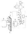
図1及び図2は、本発明に係る部品移載装置である部品実装装置(本発明に係る部品移載方法が使用される部品移載装置)を概略的に示しており、図1は装置全体を平面図で、図2は装置の要部を斜視図でそれぞれ概略的に示している。 1 and 2 schematically show a component mounting apparatus (a component transfer apparatus in which the component transfer method according to the present invention is used), which is a component transfer apparatus according to the present invention. FIG. The whole is a plan view, and FIG. 2 schematically shows the main part of the apparatus in a perspective view.
この部品実装装置1は、基台2と、この基台2上に設置されて基板Pの搬送ラインを構成するコンベア3と、ダイシングされたウエハ7が配置される部品供給部5と、この部品供給部5からチップ部品7aを吸着し、基板Pに実装する移載ヘッド4とを備えている。
This component mounting apparatus 1 includes a base 2, a conveyor 3 that is installed on the base 2 and forms a transfer line for the substrate P, a
上記コンベア3は、基台2上においてX軸方向(基板Pの搬送方向)に延びるように設置され、基板Pを上流側(−X側)から搬送して所定の実装作業位置(図示されている位置)で保持し、その基板Pに対する実装作業が終了するのを待って上記実装作業位置の下流側(+X側)に基板Pを搬出するように構成されている。なお、上記コンベア3には、基板Pを上記実装作業位置に保持するための図略のクランプ機構等が設けられている。 The conveyor 3 is installed on the base 2 so as to extend in the X-axis direction (conveyance direction of the substrate P), conveys the substrate P from the upstream side (−X side), and performs a predetermined mounting work position (not shown). The substrate P is held, and the substrate P is unloaded to the downstream side (+ X side) of the mounting operation position after the mounting operation on the substrate P is completed. The conveyor 3 is provided with an unillustrated clamping mechanism for holding the substrate P at the mounting work position.
上記部品供給部5にはウエハ供給装置6が設置されている。このウエハ供給装置6は、円盤状のシリコンウエハからなるウエハ7が碁盤目状にダイシングされて形成された多数のチップ部品7a,7a…(ウエハ片)の集合体を、ウエハ保持枠8(本発明に係るシート保持手段に相当する)に保持されたウエハシート8a(本発明に係る粘着シートに相当する)上に貼着した状態で供給するように構成されている。
A
具体的には、ウエハ供給装置6は、ウエハ7が貼付けられたウエハシート8a(以下、必要に応じてウエハ付きシートという)をウエハ保持枠8に保持した状態で上下多段に収納するウエハ収納エレベータ9と、このウエハ収納エレベータ9の前方側(−Y側)に位置する基台2上に設置されたウエハステージ10と、上記ウエハ収納エレベータ9からウエハステージ10上にウエハ保持枠8を引き出すためのコンベア11等からなる引出ユニットとを備えており、複数の種類のウエハシート8aをウエハステージ10上に入れ替え可能(選択的に供給可能)な状態で保持している。なお、当実施形態では、このウエハ供給装置6が本発明のウエハ供給手段に相当し、ウエハステージ10が、本発明におけるヘッド(後記移載ヘッド4)によるウエハ片吸着可能位置に相当する。
Specifically, the
前記ウエハシート8aは、紫外線の照射により粘着力が低下する従来周知のUVテープからなり、ウエハ付きシートは、ダイシング後、紫外線照射処理が施された状態でウエハ供給装置6に収容される。
The
上記移載ヘッド4は、X軸方向およびY軸方向に移動可能に支持されており、上記部品供給部5のウエハステージ10上に位置決めされたウエハ7の上方と、上記実装作業位置に保持された基板Pの上方とにわたって自在に移動し得るように構成されている。
The transfer head 4 is supported so as to be movable in the X-axis direction and the Y-axis direction, and is held above the
すなわち、基台2上には、Y軸方向に延びる一対の固定レール13と、第1Y軸サーボモータ14により回転駆動されるボールねじ軸15とが配設され、上記移載ヘッド4を支持するための支持フレーム16が、上記固定レール13に沿ってY軸方向に移動可能に支持されるとともに、この支持フレーム16の内部に設けられたナット部分17が上記ボールねじ軸15に螺合している。また、上記支持フレーム16には、X軸方向に延びる図略のガイド部材と、第1X軸サーボモータ18により回転駆動されるボールねじ軸19とが配設され、上記移載ヘッド4が上記ガイド部材に沿ってX軸方向に移動可能に支持されるとともに、この移載ヘッド4の内部に設けられた図略のナット部分が上記ボールねじ軸19に螺合している。そして、第1Y軸サーボモータ14が作動してボールねじ軸15が回転駆動されることにより、上記支持フレーム16が移載ヘッド4と一体にY軸方向に移動し、かつ第1X軸サーボモータ18が作動してボールねじ軸19が回転駆動されることにより、移載ヘッド4が支持フレーム16に対してX軸方向に移動する構成となっている。
That is, on the base 2, a pair of fixed
上記移載ヘッド4は、図1及び図2に示すように、上記ウエハステージ10上のウエハ7から個々のチップ部品7aを吸着するための複数の(図例では3つの)ノズルユニット30を有している。
As shown in FIGS. 1 and 2, the transfer head 4 has a plurality of (three in the illustrated example)
これら各ノズルユニット30は、その下端部に中空状のノズル部材30a(図3参照)を有しており、部品吸着時には、真空ポンプ等からなる図略の負圧供給手段から上記ノズル部材の先端部に負圧が供給され、その負圧による吸引力で上記ノズル部材30aにチップ部品7aが吸着されるようになっている。また、上記ノズルユニット30は、移載ヘッド4の本体部に対し上下方向(Z軸方向)に移動可能で、かつノズル中心軸(R軸)回りに回転可能な状態で取り付けられ、図略のZ軸サーボモータおよびR軸サーボモータによりそれぞれ各方向に駆動されるように構成されている。
Each of these
上記移載ヘッド4には、さらに基板Pの上面に付された位置認識用のフィデューシャルマーク(図示省略)を認識するための基板認識カメラ31が取り付けられており、基板Pがコンベア3によって実装作業位置まで搬送されてくると、この基板認識カメラ31が移載ヘッド4とともに上記フィデューシャルマークの上方まで移動してこれを撮像し、これによって基板Pの正確な位置を特定するように構成されている。
The transfer head 4 is further provided with a
一方、上記部品供給部5の上方には、そのウエハステージ10上に位置決めされたウエハ7の各チップ部品7aを撮像してその正確な位置を特定するための吸着位置認識カメラ32が設けられている。この吸着位置認識カメラ32は、上記移載ヘッド4と同様の機構によりX,Y軸の各方向に移動可能に支持されている。
On the other hand, a suction
すなわち、吸着位置認識カメラ32は、Y軸方向に沿って延びる一対のガイドレール33に沿って移動可能な支持フレーム36に、カメラ取付部32aを介して支持されており、上記支持フレーム36の内部に設けられたナット部分37に螺合するボールねじ軸35が、第2Y軸サーボモータ34により回転駆動されることで、上記支持フレーム36と一体にY軸方向に移動するように構成されている。また、上記支持フレーム36には、上記カメラ取付部32aの内部に設けられた図略のナット部分と螺合するボールねじ軸39が配設されており、このボールねじ軸39が第2X軸サーボモータ38により回転駆動されることで、上記吸着位置認識カメラ32がX軸方向に移動するように構成されている。
That is, the suction
また、上記部品供給部5におけるウエハステージ10の下方には、移載ヘッド4による部品吸着時に、ウエハシート8aに対してレーザー光を照射することによりチップ部品7aの剥離を支援するレーザー照射ユニット40が設けられている。このレーザー照射ユニット40は、基台2上にX軸方向およびY軸方向に移動可能に支持され、部品供給部5内のウエハステージ10に対応する程度の範囲にわたって移動し得るように構成されている。
Further, below the
すなわち、レーザー照射ユニット40は、図1中に破線で示すとともに、図2の概略斜視図にも示すように、Y軸方向に延びる一対のガイドレール41に沿って移動可能な支持フレーム42に、X軸方向に移動可能に支持されている。そして、上記支持フレーム42の内部に設けられた図略のナット部分に螺合するボールねじ軸43が、第3Y軸サーボモータ44により回転駆動されることで、レーザー照射ユニット40が上記支持フレーム42と一体にY軸方向に移動する。また、上記支持フレーム42には、レーザー照射ユニット40の内部に設けられた図略のナット部分と螺合するボールねじ軸45が配設されており、このボールねじ軸45が第3X軸サーボモータ46により回転駆動されることで、レーザー照射ユニット40がX軸方向に移動するように構成されている。
That is, the
上記レーザー照射ユニット40は、図3のブロック図に概略的に示すように、レーザー発振器50から照射されるレーザー光をウエハシート8aに照射するためのレーザー光学系と、移載ヘッド4による部品吸着時に、ウエハシート8aを吸着する吸着機構とを備えている。
As schematically shown in the block diagram of FIG. 3, the
前記レーザー光学系は、コリメートレンズユニット52、ビームスプリッター53、ポリゴンミラー54及びf・θレンズ55等を含み、レーザー発振器50から照射されるレーザー光Lをコリメートレンズユニット52で平行光に変換し、そのレーザー光LをコントローラHCにより制御されたポリゴンミラー54で目標位置に走査し、f・θレンズで集光して目標地点に照射すると共に、コリメートレンズユニット52からポリゴンミラー54に照射されるレーザー光Lの一部をビームスプリッター53で分光して光電変換装置56に導光するように構成されている。
The laser optical system includes a
レーザー発振器50は、その駆動装置57と共に前記基台2上の所定位置に固定されており、当該駆動装置57の制御に基づきレーザー光Lを照射すると共に、その照射出力が、予め設定された所定の出力値(後述する出力値)となるように、上記光電変換装置56から出力される電気信号に基づいて駆動装置57によりフィードバック制御されるように構成されている。当実施形態では、レーザー発振器50としてYAGレーザー発振器が適用されており、このレーザー発振器50から照射されたレーザー光Lは、光ファイバー51を通じてコリメートレンズユニット52に導光される構成となっている。
The
なお、この部品実装装置1では、上記レーザー照射ユニット40及びレーザー発振器50等が本発明に係るレーザー照射手段に相当し、前記駆動装置57及び後記コントローラHC等が本発明に出力制御手段に相当し、さらにコントローラHCが本発明に係る駆動制御手段に相当する。
In this component mounting apparatus 1, the
前記吸着機構(本発明に係るシート吸着手段に相当する)は、Z軸方向に昇降可能な吸着ピン60と、この吸着ピン60を駆動するエアシリンダ等の図外のアクチュエータとを含んでおり、ウエハステージ10上のウエハシート8aの下面(チップ部品7aの支持面とは反対側の面)に当接して当該ウエハシート8aを吸着する作動位置と、この位置から僅かに下降した待機位置とに亘って吸着ピン60を変位させるように構成されている。なと、前記作動位置は、ウエハステージ10上のウエハ付きシートをほぼ水平に保った状態でウエハシート8aを吸着するように高さ設定されている。
The suction mechanism (corresponding to the sheet suction means according to the present invention) includes a
前記吸着ピン60は、図3に示すように、Z軸方向に貫通するレーザー光Lの照射孔61を中心部に備えた円筒型のピンで、前記レーザー光学系により導光されるレーザー光Lをこの照射孔61を通じてウエハステージ10上のウエハ付きシートに照射させるように構成されている。なお、吸着ピン60の内径(照射孔61の径)は、ウエハシート8a越しにチップ部品7aの一部又は全部を囲むように設定されている。
As shown in FIG. 3, the
吸着ピン60の先端(上端)には平坦なサークル状の吸着面62が設けられている。この吸着面62には、図4に示すように大小複数(図示の例では2つ)の円周溝63,63が同心円上に形成されており、各円周溝63,63の内底面には、それぞれ吸引孔63aが周方向に所定間隔で設けられている。これらの吸引孔63aは、吸着ピン60内部の図外の通路、及び配管等を通じて真空ポンプ等からなる図略の負圧供給手段に連通しており、各円周溝63,63に負圧が供給されることで、その負圧による吸引力でウエハシート8aを吸着し得るようになっている。
A flat circle-shaped
なお、詳しく図示していないが、この部品実装装置1は、装置全体を統括的に制御するコントローラHCを有しており、ウエハ供給装置6によるウエハ7の出し入れ、部品実装時の移載ヘッド4やレーザー照射ユニット40の動作等は、全てこのコントローラHCにより統括的に制御されるように構成されている。以下、コントローラHCの制御に基づく部品実装装置1の部品実装動作(部品移載方法)とその作用について説明する。
Although not shown in detail, the component mounting apparatus 1 has a controller HC that comprehensively controls the entire apparatus, and the
実装処理が行なわれるときは、ウエハ付きシートを保持するウエハ保持枠8が、ウエハステージ10上にセットされて、部品の取出しが可能な状態となる。なお、この時点で、ウエハシート8aには上記の通り既に紫外線照射処理が施されており、ウエハシート8aの粘着力はある程度低下している。
When the mounting process is performed, the
実装処理が開始されると、先ず、コンベア3の作動により基板Pが図1に示される実装作業位置まで搬入され、移載ヘッド4の移動により基板認識カメラ31が基板Pの上方に配置される。これによりの基板Pの上面に付された位置認識用のフィデューシャルマークが基板認識カメラ31で撮像され、上記実装作業位置に位置決めされた基板Pの位置が認識される。そしてさらに、吸着位置認識カメラ32が、部品供給部5のウエハステージ10の上方に配置され、このウエハステージ10上のウエハ7に含まれる多数のチップ部品7a,7a…のうち、吸着予定のチップ部品7a(対象部品)が上記吸着位置認識カメラ32で撮像されることにより、上記吸着予定部品の位置が認識されると共に、その補正値が求められ、この補正値を加味した吸着予定部品の位置に移載ヘッド4(ノズルユニット30)及びレーザー照射ユニット40が配置される。なお、この時点では、レーザー照射ユニット40の吸着ピン60は待機位置にセットされており、吸着面62への負圧の供給も停止されている。レーザー光Lの照射も行われていない。また、ノズルユニット30は上昇端位置に保持されている。
When the mounting process is started, the substrate P is first carried to the mounting operation position shown in FIG. 1 by the operation of the conveyor 3, and the
レーザー照射ユニット40が吸着予定部品の位置に移動すると、前記アクチュエータの駆動により吸着ピン60が作動位置に変位すると共に前記吸着面62へ負圧が供給される。これにより、ウエハシート8aが、その下面側から吸着ピン60により吸着、保持される。
When the
そしてこの吸着ピン60によるウエハシート8aの吸着とほぼ同時に、レーザー発振器50からレーザー光Lが照射され、上記光学系により導光されることにより吸着ピン60の前記照射孔61を通じてウエハシート8aに照射されると共に、このレーザー光Lの照射に同期してノズルユニット30が駆動され、これにより図5に示すように、ノズル部材30aが降下してチップ部品に当接もしくは近接し、チップ部品7aの吸着が正確に行われる。
Nearly simultaneously with the adsorption of the
なお、レーザー発振器50によるレーザー光の出力は、ウエハシート8aのうちレーザー光の照射位置を含むその近傍が適度に熱変形(収縮又は膨張)する程度の出力となるように、前記コントローラHC等により制御されており、このように出力制御されたレーザー光が上記ウエハシート8aに照射されることで、ウエハシート8aからのチップ部品7aの剥離が円滑に行われ、当該チップ部品7aの吸着が適切に行われる。すなわち、紫外線照射処理により硬化し粘着力が低下したウエハシート8aにレーザー光を照射して適度な熱変形(収縮又は膨張)を与えると、当該熱変形に伴いチップ部品7aとウエハシート8aとの間にせん断力等、チップ部品7aの剥離を促進させる力が作用し、従って、このような状態の当該チップ部品7aに対してノズルユニット30による負圧が作用することで、ウエハシート8aから容易にチップ部品7aが剥離されて吸着されることとなる。
The laser light output by the
こうしてチップ部品7aがノズル部材30aによって吸着保持されると、移載ヘッド4が基板P上の実装箇所の上方に配置された後、ノズルユニット30が昇降駆動されることによりチップ部品7aが基板Pに実装される。これによってチップ部品7aの一連の実装処理が完了する。
When the
以上説明したように、この部品実装装置1(部品移載方法)では、レーザー光をウエハシート8aに照射してチップ部品7aを剥離等させるが、従来のように吸着予定部品の位置にレーザー光を照射して当該部分を除去(レーザーアブレーション)するのではなく、ウエハシート8aを収縮又は膨張させることによりチップ部品7aに対するウエハシート8aの貼付け面に適度な熱変形を与えてチップ部品7をウエハシート8aから剥離する、又は剥離を促すようにしているので、ウエハシートを除去する従来方法のように、チップ部品7aへのレーザー光によるダメージ、有機物等の付着や当該除去に伴うチップ部品7aの飛散といった不都合や、欠落部分(開口)が徐々に増大してウエハシート8aの安定性が損なわれるという不都合を伴うことなくチップ部品7aをウエハシート8aから剥離し、又剥離を促進させることができる。
As described above, in this component mounting apparatus 1 (component transfer method), the laser light is applied to the
従って、ウエハシート8aにレーザー光Lを照射してチップ部品7aを剥離しながらも、従来に比してチップ部品7aをより良好に、かつ安定的にウエハシート8aから剥離して基板Pに実装(移載)することができるという効果がある。
Therefore, while the
特に、この部品実装装置1(部品移載方法)では、吸着ピン60によりウエハシート8aを吸着した状態で、ノズルユニット30によりチップ部品7aを吸着するようにしているので、ノズルユニット30によるチップ部品持ち上げ時にウエハシート8aがチップ部品7aに追従するといった現象を有効に阻止することができ、ウエハシート8aからのチップ部品7aの剥離をより円滑に、かつ速やかに行わせることができるという利点もある。
In particular, in this component mounting apparatus 1 (component transfer method), the
しかも、この部品実装装置1(部品移載方法)では、この吸着ピン60を円筒形状とし、ウエハシート8aのうち、吸着対象となるチップ部品7aの一部又は全部を囲むように吸着ピン60によりウエハシート8aを吸着支持した状態で、その内側領域にレーザー光を照射するようにしているので、当該レーザー光の照射により、ウエハシート8aのうち吸着対象となるチップ部品7aに対応する部分周辺へ熱変形が拡大することを緩和することができ、その結果、当該周辺部分のチップ部品7aが不意にウエハシート8aから剥離するといった不都合を未然に防止することができるという利点もある。
Moreover, in this component mounting apparatus 1 (component transfer method), the
また、上記の説明では言及していないが、この部品実装装置1(部品移載方法)では、ウエハシート8aのうち吸着対象となるチップ部品7aの内側(輪郭よりも内側の部分)にレーザー光Lを照射すると共に、ポリゴンミラー54の駆動によりウエハシート8aを所定の経路に沿って走査するようにレーザー光学系が構成されている。従って、チップ部品7aの形状(貼付けられた面の形状)に応じて、チップ部品7aの剥離を促進させ得る位置に対して上記出力制御されたレーザー光Lを効率良く照射することができるという利点がある。ここで、具体的な走査経路や走査範囲は、チップ部品7aの形状等に応じて異なり、それに応じて設定すれば良い。ウエハシート8aに対するチップ部品7aの貼付け面の形状が矩形の場合には、レーザー光Lの走査経路や走査範囲としては、例えば図6(a)〜(f)に示すものが考えられる(同図中の斜線部分がレーザー光照射部分を示す)が、特に角部では剥離が生じ易いので、同図(d)、(f)のようにチップ部品7aの角部に対してレーザー光Lを照射するのが好ましい。なお、この構成ではレーザー光学系に組み込まれるポリゴンミラー54等が本発明に係る照射位置可変手段に相当する。
Although not mentioned in the above description, in this component mounting apparatus 1 (component transfer method), laser light is applied to the inside (portion inside the contour) of the
更に、この部品実装装置1(部品移載方法)では、ウエハシート8aのうち吸着対象となるチップ部品7aのみを、ウエハシート8aを安定な状態に保ちながら剥離できることから、ウエハ供給装置6において、複数の種類のウエハシート8aをウエハステージ10上に入れ替えすることで、基板Pに異なる種類のチップ部品Pを実装することができるという効果がある。
Furthermore, in this component mounting apparatus 1 (component transfer method), only the
次に、第2の実施形態に係る部品実装装置1について説明する。 Next, a component mounting apparatus 1 according to the second embodiment will be described.
図7は、第2の実施形態に係る部品実装装置1の要部、具体的にはレーザー照射ユニット40の構成を示している。この図に示すように、第2の実施形態に係る部品実装装置1は、主にレーザー光学系の構成が第1の実施形態と相違している。
FIG. 7 shows the configuration of the main part of the component mounting apparatus 1 according to the second embodiment, specifically, the
このレーザー光学系は、コリメートレンズユニット52、アッテネータユニット65、ビームスプリッター53、ビームエキスパンダー66、ビーム成型用スリット67、集光レンズ68、ミラー69等を含み、レーザー発振器50から照射されるレーザー光Lを平行光に変換し、このレーザー光Lをビームエキスパンダー66で拡張した後、ビーム成型用スリット67を透過させて集光レンズ68で集光しながらミラー69で目標地点に導光、照射する構成となっている。ポリゴンミラー54に照射されるレーザー光Lの一部は、ビームスプリッター53で分光されてアッテネータユニット65に導光されており、アッテネータユニット65は、当該分光光量に基づき、ウエハシート8aに照射されるレーザー光Lの光量が予め設定された設定光量(つまり出力値)、つまりウエハシート8aが収縮又は膨張による熱変形を生じる程度の光量となるようにコリメートレンズユニット52からのレーザー光Lの透過率を制御するようになっている。つまり、この実施形態では、アッテネータユニット65及びコントローラHC等が本発明に係る出力制御手段に相当する。
This laser optical system includes a
なお、ビーム成型用スリット67は、レーザー光Lの照射位置や範囲を制御するテンプレートで、レーザー光Lの照射位置や範囲に対応した開口を有し、この開口を通じてレーザー光Lを透過させるように構成されている。具体的には図6(a)〜(f)の斜線部分に対応する開口を備えた構成とされており、レーザー光Lを透過させることにより同図に示す照射位置や範囲にレーザー光Lを照射させるように構成されている。 The beam shaping slit 67 is a template for controlling the irradiation position and range of the laser light L, has an opening corresponding to the irradiation position and range of the laser light L, and transmits the laser light L through the opening. It is configured. Specifically, an opening corresponding to the hatched portion in FIGS. 6A to 6F is provided, and the laser beam L is transmitted to the irradiation position and range shown in FIG. It is comprised so that it may irradiate.
つまり、第1の実施形態では、ポリゴンミラー54の駆動によりレーザー光Lでウエハシート8aを走査することにより図6に示すような位置及び範囲でレーザー光Lをウエハシート8aに照射する構成となっているのに対して、第2の実施形態は、予めビーム成型用スリット67にレーザー光Lを透過させることにより、図6に示すような位置及び範囲にレーザー光Lを照射する構成となっている。このような第2の実施形態でも、基本的には第1の実施形態と同様の作用効果を享受することが可能であるが、第1の実施形態のものに比べるとレーザー光学系を安価に構成できるという利点がある。
That is, in the first embodiment, the
ところで、上述した部品実装装置1は、本発明に係る部品移載装置(本発明に係る部品移載方法が使用される部品移載装置)の一実施形態であって、その具体的な構成や部品移載方法は本発明の要旨を逸脱しない範囲で適宜変更可能である。 By the way, the component mounting apparatus 1 described above is an embodiment of a component transfer apparatus according to the present invention (a component transfer apparatus in which the component transfer method according to the present invention is used). The parts transfer method can be appropriately changed without departing from the gist of the present invention.
例えば、各実施形態では、レーザー発振器50としてYAGレーザーを適用しているが、CO2レーザーやエキシマレーザー等、他のレーザー発振器を適用してもよい。
For example, in each embodiment, a YAG laser is applied as the
また、第1の実施形態では、本発明に係る照射位置可変手段としてポリゴンミラー54等をレーザー光学系に組み込み、当該ポリゴンミラー54の作動によりウエハシート8aをレーザー光Lで走査するようにしているが、勿論、ガルバノメータ等、その他の要素(構成)を用いてレーザー光Lでウエハシート8aを走査するように構成してもよい。
In the first embodiment, a polygon mirror 54 or the like is incorporated in the laser optical system as the irradiation position changing means according to the present invention, and the
また、図示を省略するが、ウエハシート8a(吸着対象となるチップ部品7aに対応する部分)にクリーンエア、あるいは窒素(N2)等の気体を吹き付ける吹き付け手段をレーザー照射ユニット40等に搭載し、レーザー光Lの照射時に併せて気体をウエハシート8aに吹き付けるように前記コントローラHCにより当該吹き付け手段を制御するように構成してもよい。この構成によれば、気体の吹き付けにより、ウエハシート8aに振動を与えることができ、その結果、チップ部品7aの剥離をより促進させることが可能となる。この場合には、例えばレーザー照射ユニット40の本体部分にノズルを設け、このノズルから吸着ピン60の前記照射孔61を通じてウエハシート8aに気体を吹き付けるようにすれば、チップ部品7aの剥離を促進させることができる一方で、外部への気体の飛散を抑えることが可能となる。
Although not shown, a spraying means for spraying a gas such as clean air or nitrogen (N2) on the
また、実施形態では、本発明を、シリコンウエハ(ウエハ7)からチップ部品7aを吸着して基板P上に実装(移載)する装置に適用した例について説明したが、勿論、セラミックや樹脂、その他の材料からなるチップ部品を移載する装置についてもレーザー光による基板に与えるダメージの少ない本発明は有用である。
In the embodiment, the example in which the present invention is applied to an apparatus for adsorbing the
1 部品実装装置
4 移載ヘッド
6 ウエハ供給装置
7 ウエハ
7a チップ部品
8a ウエハシート
10 ウエハステージ
30 ノズルユニット
40 レーザー照射ユニット
50 レーザー発振器
L レーザー光
P 基板
DESCRIPTION OF SYMBOLS 1 Component mounting apparatus 4
Claims (11)
出力制御されたレーザー光を、前記粘着シートのうち移載対象となるウエハ片が保持されている部分に照射することにより当該部分を収縮又は膨張させ、ヘッドによりウエハ片を吸着することにより前記粘着シートから剥離し、前記目標地点に移載することを特徴とする部品移載方法。 A method of peeling a wafer piece held on an adhesive sheet in a state of being divided into a plurality from the adhesive sheet and transferring it to a target point,
By irradiating the portion of the adhesive sheet on which the wafer piece to be transferred is held with the output-controlled laser light, the portion is contracted or expanded, and the wafer piece is adsorbed by the head by adsorbing the wafer piece. A component transfer method, wherein the component is peeled from the sheet and transferred to the target point.
前記粘着シートは紫外線照射により粘着力が低下するUVテープからなり、前記レーザー光の照射前に、予め紫外線を粘着シートに照射しておくことを特徴とする部品移載方法。 In the component transfer method according to claim 1,
The component transfer method, wherein the pressure-sensitive adhesive sheet is made of a UV tape whose adhesive strength is reduced by ultraviolet irradiation, and the ultraviolet-ray is irradiated to the pressure-sensitive adhesive sheet in advance before the laser light irradiation.
前記ウエハ片の保持面とは反対側から前記粘着シートを吸着するシート吸着手段を用い、このシート吸着手段により前記粘着シートを吸着、保持した状態で、前記ヘッドによりウエハ片を吸着させることを特徴とする部品移載方法。 In the component transfer method according to claim 1 or 2,
A sheet adsorbing unit that adsorbs the adhesive sheet from the side opposite to the holding surface of the wafer piece is used, and the wafer piece is adsorbed by the head while the adhesive sheet is adsorbed and held by the sheet adsorbing unit. The parts transfer method.
前記粘着シートのうち、移載対象となるウエハ片の一部又は全部を囲むように前記シート吸着手段により粘着シートを吸着した状態で、その内側領域に前記レーザー光を照射することを特徴とする部品移載方法。 In the parts transfer method according to claim 3,
The inside of the adhesive sheet is irradiated with the laser beam in a state where the adhesive sheet is adsorbed by the sheet adsorbing means so as to surround a part or all of a wafer piece to be transferred. Parts transfer method.
前記ウエハ片が粘着シートに対して貼付けられた面が矩形をなし、当該貼付けられた面の角部に前記レーザー光を照射することを特徴とする部品移載方法。 In the parts transfer method according to any one of claims 1 to 4,
A part transfer method, wherein a surface of the wafer piece attached to the adhesive sheet is rectangular, and the laser light is irradiated to a corner of the attached surface.
粘着シート上のウエハ片を吸着して目標地点に移載するヘッドと、
前記粘着シートのうち移載対象となるウエハ片が保持されている部分に対してレーザー光を照射するレーザー照射手段と、
前記粘着シートが収縮又は膨張するように、前記レーザー照射手段から照射されるレーザー光の出力を制御する出力制御手段と、
前記レーザー光を照射した状態で、移載対象となるウエハ片を吸着するように前記レーザー照射手段、及びヘッドの駆動を制御する駆動制御手段と、を備えていることを特徴とする部品移載装置。 An apparatus for separating and transferring the wafer piece held on the adhesive sheet in a state of being divided into a plurality of wafer pieces from the adhesive sheet,
A head that adsorbs a wafer piece on an adhesive sheet and transfers it to a target point;
Laser irradiation means for irradiating a portion of the pressure-sensitive adhesive sheet on which a wafer piece to be transferred is held with laser light;
Output control means for controlling the output of laser light emitted from the laser irradiation means so that the adhesive sheet contracts or expands;
Component transfer comprising the laser irradiation means and a drive control means for controlling the drive of the head so as to attract the wafer piece to be transferred in a state of being irradiated with the laser light. apparatus.
前記ウエハ片の保持面とは反対側から前記粘着シートを吸着するシート吸着手段をさらに備え、前記駆動制御手段は、このシート吸着手段により前記粘着シートを吸着、保持した状態で、前記ヘッドによるウエハ片の吸着が行われるように当該シート吸着手段、及び前記ヘッドを駆動制御することを特徴とする部品移載装置。 In the component transfer apparatus of Claim 6,
The apparatus further includes a sheet adsorbing unit that adsorbs the adhesive sheet from the side opposite to the holding surface of the wafer piece, and the drive control unit adsorbs and holds the adhesive sheet by the sheet adsorbing unit, and the wafer by the head. A component transfer apparatus that controls driving of the sheet suction means and the head so that the pieces are sucked.
前記シート吸着手段は、移載対象となるウエハ片の一部又は全部を囲んだ状態で粘着シートを吸着し得るようにサークル状の吸着面を有し、前記レーザー照射手段は、前記吸着面の内側領域にレーザー光を照射するように構成されていることを特徴とする部品移載装置。 In the component transfer apparatus according to claim 7,
The sheet adsorbing means has a circle-shaped adsorbing surface so that the adhesive sheet can be adsorbed in a state of surrounding a part or all of a wafer piece to be transferred, and the laser irradiation means A component transfer device configured to irradiate an inner region with laser light.
前記駆動制御手段は、前記粘着シートをシート吸着手段により吸着した状態で、当該粘着シートに対してレーザー光を照射するように、前記シート吸着手段、及び前記レーザー照射手段を駆動制御することを特徴とする部品移載装置。 In the component transfer apparatus according to claim 8,
The drive control unit drives and controls the sheet adsorption unit and the laser irradiation unit so that the adhesive sheet is irradiated with laser light in a state where the adhesive sheet is adsorbed by the sheet adsorption unit. A parts transfer device.
前記レーザー照射手段は、レーザー光の照射位置を可変とする照射位置可変手段を含み、前記駆動制御手段は、予め定められた所定経路に沿って前記レーザー光で粘着シートを走査するように前記レーザー照射手段を駆動制御することを特徴とする部品移載装置。 In the component transfer apparatus according to any one of claims 6 to 8,
The laser irradiating means includes an irradiation position changing means for changing an irradiation position of laser light, and the drive control means scans the adhesive sheet with the laser light along a predetermined path. A component transfer apparatus that controls driving of an irradiation unit.
前記ウエハ付きの粘着シートを複数保持し、かつこれらウエハ付きの粘着シートを、前記ヘッドによるウエハ片吸着可能位置に対して選択的に供給するウエハ供給手段を備えていることを特徴とする部品移載装置。 In the component transfer apparatus as described in any one of Claims 6 thru | or 10,
There is provided a wafer transfer means for holding a plurality of the pressure-sensitive adhesive sheets with the wafer and selectively supplying the pressure-sensitive adhesive sheets with the wafer to a position where the wafer piece can be adsorbed by the head. Mounting device.
Priority Applications (1)
| Application Number | Priority Date | Filing Date | Title |
|---|---|---|---|
| JP2008147019A JP2009295741A (en) | 2008-06-04 | 2008-06-04 | Method and apparatus for transferring components |
Applications Claiming Priority (1)
| Application Number | Priority Date | Filing Date | Title |
|---|---|---|---|
| JP2008147019A JP2009295741A (en) | 2008-06-04 | 2008-06-04 | Method and apparatus for transferring components |
Publications (2)
| Publication Number | Publication Date |
|---|---|
| JP2009295741A true JP2009295741A (en) | 2009-12-17 |
| JP2009295741A5 JP2009295741A5 (en) | 2011-04-07 |
Family
ID=41543679
Family Applications (1)
| Application Number | Title | Priority Date | Filing Date |
|---|---|---|---|
| JP2008147019A Pending JP2009295741A (en) | 2008-06-04 | 2008-06-04 | Method and apparatus for transferring components |
Country Status (1)
| Country | Link |
|---|---|
| JP (1) | JP2009295741A (en) |
Cited By (2)
| Publication number | Priority date | Publication date | Assignee | Title |
|---|---|---|---|---|
| JP2020053558A (en) * | 2018-09-27 | 2020-04-02 | 東レエンジニアリング株式会社 | Transfer method, method of manufacturing image display device using the same, and transfer device |
| WO2022244033A1 (en) * | 2021-05-17 | 2022-11-24 | ヤマハ発動機株式会社 | Component transfer device |
Citations (5)
| Publication number | Priority date | Publication date | Assignee | Title |
|---|---|---|---|---|
| JPH0442557A (en) * | 1990-06-08 | 1992-02-13 | Sumitomo Electric Ind Ltd | Chip-shaped part pickup apparatus |
| JPH09115986A (en) * | 1995-10-20 | 1997-05-02 | Fujitsu Ltd | Manufacture of semiconductor device |
| JP2002164414A (en) * | 2000-11-27 | 2002-06-07 | Shinkawa Ltd | Method and apparatus for processing semiconductor pellet |
| JP2002353253A (en) * | 2001-05-24 | 2002-12-06 | Nec Kansai Ltd | Device and method for supplying semiconductor chip |
| JP2008060393A (en) * | 2006-08-31 | 2008-03-13 | Shibuya Kogyo Co Ltd | Pickup device for plate-like article |
-
2008
- 2008-06-04 JP JP2008147019A patent/JP2009295741A/en active Pending
Patent Citations (5)
| Publication number | Priority date | Publication date | Assignee | Title |
|---|---|---|---|---|
| JPH0442557A (en) * | 1990-06-08 | 1992-02-13 | Sumitomo Electric Ind Ltd | Chip-shaped part pickup apparatus |
| JPH09115986A (en) * | 1995-10-20 | 1997-05-02 | Fujitsu Ltd | Manufacture of semiconductor device |
| JP2002164414A (en) * | 2000-11-27 | 2002-06-07 | Shinkawa Ltd | Method and apparatus for processing semiconductor pellet |
| JP2002353253A (en) * | 2001-05-24 | 2002-12-06 | Nec Kansai Ltd | Device and method for supplying semiconductor chip |
| JP2008060393A (en) * | 2006-08-31 | 2008-03-13 | Shibuya Kogyo Co Ltd | Pickup device for plate-like article |
Cited By (2)
| Publication number | Priority date | Publication date | Assignee | Title |
|---|---|---|---|---|
| JP2020053558A (en) * | 2018-09-27 | 2020-04-02 | 東レエンジニアリング株式会社 | Transfer method, method of manufacturing image display device using the same, and transfer device |
| WO2022244033A1 (en) * | 2021-05-17 | 2022-11-24 | ヤマハ発動機株式会社 | Component transfer device |
Similar Documents
| Publication | Publication Date | Title |
|---|---|---|
| KR102285101B1 (en) | Inspection method, inspection apparatus, laser machining apparatus and expansion apparatus of workpiece | |
| US7544588B2 (en) | Laser processing method for wafer | |
| US7605058B2 (en) | Wafer dividing method | |
| US7888239B2 (en) | Semiconductor device manufacturing method | |
| JP2009064905A (en) | Extension method and extension apparatus | |
| JP5443102B2 (en) | Laser processing equipment | |
| KR102343533B1 (en) | Method for dividing workpiece and laser machining apparatus | |
| CN107452609B (en) | Wafer processing method | |
| JP2010153692A (en) | Workpiece dividing method and tape expanding device | |
| TWI539502B (en) | Protective material and ablation processing method | |
| KR20140118757A (en) | Wafer machining method | |
| CN111326454A (en) | Method for manufacturing element array and method for removing specific element | |
| JP2016147342A (en) | Chuck table for processing device | |
| JP4766258B2 (en) | Pickup device for plate-like article | |
| TWI813824B (en) | Wafer processing method | |
| JP2009295741A (en) | Method and apparatus for transferring components | |
| JP2009295741A5 (en) | ||
| JP7154687B2 (en) | tape expansion unit | |
| JP5913859B2 (en) | Electrical cooling device | |
| JP2006324373A (en) | Method and device of pickup of chip | |
| TWI812847B (en) | Wafer processing method | |
| JP2012182278A (en) | Laser lift-off device and laser lift-off method | |
| JP2014140856A (en) | Laser processing device | |
| CN111326469A (en) | Device for manufacturing element array and device for removing specific element | |
| JP2017079284A (en) | Laser beam machining device |
Legal Events
| Date | Code | Title | Description |
|---|---|---|---|
| A521 | Written amendment |
Free format text: JAPANESE INTERMEDIATE CODE: A523 Effective date: 20110221 |
|
| A621 | Written request for application examination |
Free format text: JAPANESE INTERMEDIATE CODE: A621 Effective date: 20110221 |
|
| A871 | Explanation of circumstances concerning accelerated examination |
Free format text: JAPANESE INTERMEDIATE CODE: A871 Effective date: 20110221 |
|
| A977 | Report on retrieval |
Free format text: JAPANESE INTERMEDIATE CODE: A971007 Effective date: 20110622 |
|
| A975 | Report on accelerated examination |
Free format text: JAPANESE INTERMEDIATE CODE: A971005 Effective date: 20110622 |
|
| A131 | Notification of reasons for refusal |
Free format text: JAPANESE INTERMEDIATE CODE: A131 Effective date: 20110628 |
|
| A521 | Written amendment |
Free format text: JAPANESE INTERMEDIATE CODE: A523 Effective date: 20110826 |
|
| A02 | Decision of refusal |
Free format text: JAPANESE INTERMEDIATE CODE: A02 Effective date: 20111004 |