JP2009267219A - Semiconductor memory device and manufacturing method thereof - Google Patents
Semiconductor memory device and manufacturing method thereof Download PDFInfo
- Publication number
- JP2009267219A JP2009267219A JP2008117055A JP2008117055A JP2009267219A JP 2009267219 A JP2009267219 A JP 2009267219A JP 2008117055 A JP2008117055 A JP 2008117055A JP 2008117055 A JP2008117055 A JP 2008117055A JP 2009267219 A JP2009267219 A JP 2009267219A
- Authority
- JP
- Japan
- Prior art keywords
- amorphous silicon
- memory device
- semiconductor memory
- manufacturing
- conductivity type
- Prior art date
- Legal status (The legal status is an assumption and is not a legal conclusion. Google has not performed a legal analysis and makes no representation as to the accuracy of the status listed.)
- Withdrawn
Links
- 239000004065 semiconductor Substances 0.000 title claims abstract description 166
- 238000004519 manufacturing process Methods 0.000 title claims description 104
- 230000015654 memory Effects 0.000 claims abstract description 146
- 239000012535 impurity Substances 0.000 claims abstract description 108
- 239000000463 material Substances 0.000 claims abstract description 86
- 229910052751 metal Inorganic materials 0.000 claims abstract description 52
- 239000002184 metal Substances 0.000 claims abstract description 52
- 238000002425 crystallisation Methods 0.000 claims abstract description 20
- 230000008025 crystallization Effects 0.000 claims abstract description 20
- XUIMIQQOPSSXEZ-UHFFFAOYSA-N Silicon Chemical compound [Si] XUIMIQQOPSSXEZ-UHFFFAOYSA-N 0.000 claims abstract description 14
- 229910052710 silicon Inorganic materials 0.000 claims abstract description 14
- 239000010703 silicon Substances 0.000 claims abstract description 14
- 238000000137 annealing Methods 0.000 claims abstract description 12
- 229910021417 amorphous silicon Inorganic materials 0.000 claims description 193
- 238000000034 method Methods 0.000 claims description 124
- 229910052721 tungsten Inorganic materials 0.000 claims description 64
- 239000012782 phase change material Substances 0.000 claims description 58
- 238000005468 ion implantation Methods 0.000 claims description 26
- 239000000758 substrate Substances 0.000 claims description 19
- 238000000151 deposition Methods 0.000 claims description 14
- 238000000059 patterning Methods 0.000 claims description 11
- 230000008569 process Effects 0.000 claims description 6
- 239000002210 silicon-based material Substances 0.000 claims description 4
- 229910021420 polycrystalline silicon Inorganic materials 0.000 abstract description 84
- 229920005591 polysilicon Polymers 0.000 abstract description 84
- 230000008859 change Effects 0.000 abstract description 78
- 238000005224 laser annealing Methods 0.000 abstract description 52
- 238000010438 heat treatment Methods 0.000 abstract description 16
- 230000004913 activation Effects 0.000 abstract description 2
- 230000036961 partial effect Effects 0.000 description 76
- WFKWXMTUELFFGS-UHFFFAOYSA-N tungsten Chemical compound [W] WFKWXMTUELFFGS-UHFFFAOYSA-N 0.000 description 57
- 239000010937 tungsten Substances 0.000 description 57
- 229910021332 silicide Inorganic materials 0.000 description 46
- FVBUAEGBCNSCDD-UHFFFAOYSA-N silicide(4-) Chemical compound [Si-4] FVBUAEGBCNSCDD-UHFFFAOYSA-N 0.000 description 46
- 230000015572 biosynthetic process Effects 0.000 description 45
- ATJFFYVFTNAWJD-UHFFFAOYSA-N Tin Chemical compound [Sn] ATJFFYVFTNAWJD-UHFFFAOYSA-N 0.000 description 35
- 150000002500 ions Chemical class 0.000 description 19
- 230000004888 barrier function Effects 0.000 description 18
- 239000007772 electrode material Substances 0.000 description 18
- 229910008484 TiSi Inorganic materials 0.000 description 17
- 238000005229 chemical vapour deposition Methods 0.000 description 17
- 238000004544 sputter deposition Methods 0.000 description 17
- 230000002829 reductive effect Effects 0.000 description 12
- VYPSYNLAJGMNEJ-UHFFFAOYSA-N Silicium dioxide Chemical compound O=[Si]=O VYPSYNLAJGMNEJ-UHFFFAOYSA-N 0.000 description 11
- 229910052814 silicon oxide Inorganic materials 0.000 description 11
- 238000009792 diffusion process Methods 0.000 description 9
- 230000000694 effects Effects 0.000 description 9
- 229910010413 TiO 2 Inorganic materials 0.000 description 8
- 229910000577 Silicon-germanium Inorganic materials 0.000 description 6
- 229910052698 phosphorus Inorganic materials 0.000 description 6
- 239000011574 phosphorus Substances 0.000 description 6
- -1 phosphorus ions Chemical class 0.000 description 6
- 238000003491 array Methods 0.000 description 5
- 238000007796 conventional method Methods 0.000 description 5
- 230000002093 peripheral effect Effects 0.000 description 5
- 238000010586 diagram Methods 0.000 description 4
- 238000002844 melting Methods 0.000 description 4
- 230000008018 melting Effects 0.000 description 4
- 239000013078 crystal Substances 0.000 description 3
- 238000013500 data storage Methods 0.000 description 3
- 230000009467 reduction Effects 0.000 description 3
- 230000002441 reversible effect Effects 0.000 description 3
- 238000001816 cooling Methods 0.000 description 2
- 230000006866 deterioration Effects 0.000 description 2
- 238000005516 engineering process Methods 0.000 description 2
- 230000010354 integration Effects 0.000 description 2
- 238000005498 polishing Methods 0.000 description 2
- 239000000126 substance Substances 0.000 description 2
- 230000003213 activating effect Effects 0.000 description 1
- 230000002411 adverse Effects 0.000 description 1
- 230000015556 catabolic process Effects 0.000 description 1
- 229910052802 copper Inorganic materials 0.000 description 1
- 230000003247 decreasing effect Effects 0.000 description 1
- 230000008021 deposition Effects 0.000 description 1
- 238000001312 dry etching Methods 0.000 description 1
- 230000006870 function Effects 0.000 description 1
- 230000006872 improvement Effects 0.000 description 1
- 238000002955 isolation Methods 0.000 description 1
- 239000007788 liquid Substances 0.000 description 1
- 238000001459 lithography Methods 0.000 description 1
- 230000014759 maintenance of location Effects 0.000 description 1
- 239000007769 metal material Substances 0.000 description 1
- 230000002265 prevention Effects 0.000 description 1
- 230000003252 repetitive effect Effects 0.000 description 1
- 238000010187 selection method Methods 0.000 description 1
- 238000003860 storage Methods 0.000 description 1
- 238000000859 sublimation Methods 0.000 description 1
- 230000008022 sublimation Effects 0.000 description 1
Images


Classifications
-
- H—ELECTRICITY
- H10—SEMICONDUCTOR DEVICES; ELECTRIC SOLID-STATE DEVICES NOT OTHERWISE PROVIDED FOR
- H10B—ELECTRONIC MEMORY DEVICES
- H10B63/00—Resistance change memory devices, e.g. resistive RAM [ReRAM] devices
- H10B63/80—Arrangements comprising multiple bistable or multi-stable switching components of the same type on a plane parallel to the substrate, e.g. cross-point arrays
- H10B63/84—Arrangements comprising multiple bistable or multi-stable switching components of the same type on a plane parallel to the substrate, e.g. cross-point arrays arranged in a direction perpendicular to the substrate, e.g. 3D cell arrays
-
- H—ELECTRICITY
- H10—SEMICONDUCTOR DEVICES; ELECTRIC SOLID-STATE DEVICES NOT OTHERWISE PROVIDED FOR
- H10B—ELECTRONIC MEMORY DEVICES
- H10B63/00—Resistance change memory devices, e.g. resistive RAM [ReRAM] devices
- H10B63/20—Resistance change memory devices, e.g. resistive RAM [ReRAM] devices comprising selection components having two electrodes, e.g. diodes
-
- H—ELECTRICITY
- H01—ELECTRIC ELEMENTS
- H01L—SEMICONDUCTOR DEVICES NOT COVERED BY CLASS H10
- H01L21/00—Processes or apparatus adapted for the manufacture or treatment of semiconductor or solid state devices or of parts thereof
- H01L21/02—Manufacture or treatment of semiconductor devices or of parts thereof
- H01L21/02104—Forming layers
- H01L21/02365—Forming inorganic semiconducting materials on a substrate
- H01L21/02518—Deposited layers
- H01L21/02521—Materials
- H01L21/02524—Group 14 semiconducting materials
- H01L21/02532—Silicon, silicon germanium, germanium
-
- H—ELECTRICITY
- H01—ELECTRIC ELEMENTS
- H01L—SEMICONDUCTOR DEVICES NOT COVERED BY CLASS H10
- H01L21/00—Processes or apparatus adapted for the manufacture or treatment of semiconductor or solid state devices or of parts thereof
- H01L21/02—Manufacture or treatment of semiconductor devices or of parts thereof
- H01L21/02104—Forming layers
- H01L21/02365—Forming inorganic semiconducting materials on a substrate
- H01L21/02656—Special treatments
- H01L21/02664—Aftertreatments
- H01L21/02667—Crystallisation or recrystallisation of non-monocrystalline semiconductor materials, e.g. regrowth
- H01L21/02675—Crystallisation or recrystallisation of non-monocrystalline semiconductor materials, e.g. regrowth using laser beams
-
- H—ELECTRICITY
- H10—SEMICONDUCTOR DEVICES; ELECTRIC SOLID-STATE DEVICES NOT OTHERWISE PROVIDED FOR
- H10N—ELECTRIC SOLID-STATE DEVICES NOT OTHERWISE PROVIDED FOR
- H10N70/00—Solid-state devices having no potential barriers, and specially adapted for rectifying, amplifying, oscillating or switching
- H10N70/20—Multistable switching devices, e.g. memristors
- H10N70/231—Multistable switching devices, e.g. memristors based on solid-state phase change, e.g. between amorphous and crystalline phases, Ovshinsky effect
-
- H—ELECTRICITY
- H10—SEMICONDUCTOR DEVICES; ELECTRIC SOLID-STATE DEVICES NOT OTHERWISE PROVIDED FOR
- H10N—ELECTRIC SOLID-STATE DEVICES NOT OTHERWISE PROVIDED FOR
- H10N70/00—Solid-state devices having no potential barriers, and specially adapted for rectifying, amplifying, oscillating or switching
- H10N70/801—Constructional details of multistable switching devices
- H10N70/821—Device geometry
- H10N70/826—Device geometry adapted for essentially vertical current flow, e.g. sandwich or pillar type devices
-
- H—ELECTRICITY
- H10—SEMICONDUCTOR DEVICES; ELECTRIC SOLID-STATE DEVICES NOT OTHERWISE PROVIDED FOR
- H10N—ELECTRIC SOLID-STATE DEVICES NOT OTHERWISE PROVIDED FOR
- H10N70/00—Solid-state devices having no potential barriers, and specially adapted for rectifying, amplifying, oscillating or switching
- H10N70/801—Constructional details of multistable switching devices
- H10N70/881—Switching materials
- H10N70/882—Compounds of sulfur, selenium or tellurium, e.g. chalcogenides
- H10N70/8828—Tellurides, e.g. GeSbTe
-
- H—ELECTRICITY
- H10—SEMICONDUCTOR DEVICES; ELECTRIC SOLID-STATE DEVICES NOT OTHERWISE PROVIDED FOR
- H10N—ELECTRIC SOLID-STATE DEVICES NOT OTHERWISE PROVIDED FOR
- H10N70/00—Solid-state devices having no potential barriers, and specially adapted for rectifying, amplifying, oscillating or switching
- H10N70/801—Constructional details of multistable switching devices
- H10N70/881—Switching materials
- H10N70/883—Oxides or nitrides
- H10N70/8833—Binary metal oxides, e.g. TaOx
Landscapes
- Semiconductor Memories (AREA)
- Recrystallisation Techniques (AREA)
Abstract
Description
本発明は半導体集積回路装置及びその製造方法に関し、特に電気的書き換えが可能な不揮発性半導体記憶装置の高集積化、高性能化を実現する技術に関する。 The present invention relates to a semiconductor integrated circuit device and a method for manufacturing the same, and more particularly to a technique for realizing high integration and high performance of an electrically rewritable nonvolatile semiconductor memory device.
電気的書き換えが可能な不揮発性半導体記憶装置のうち、一括消去が可能なものとしていわゆるフラッシュメモリが知られている。フラッシュメモリは携帯性、耐衝撃性に優れ、電気的に一括消去が可能なことから、近年、携帯型パーソナルコンピュータやデジタルスチルカメラ等の小型携帯情報機器の記憶装置として急速に需要が拡大している。その市場の拡大にはメモリセル面積の縮小によるビットコストの低減が重要な要素であり、これを実現する様々なメモリセル方式が提案されている。 Among nonvolatile semiconductor memory devices that can be electrically rewritten, a so-called flash memory is known as a device capable of batch erasure. Since flash memory has excellent portability and impact resistance and can be erased electrically in bulk, in recent years, the demand for flash memory has rapidly expanded as a storage device for small portable information devices such as portable personal computers and digital still cameras. Yes. In order to expand the market, reduction of the bit cost by reducing the memory cell area is an important factor, and various memory cell systems for realizing this have been proposed.
非特許文献1、2には大容量化に適するコンタクトレス型セルの一種である、いわゆるNAND型フラッシュメモリの例が報告されている。これらの構造を用いることによってメモリセルの物理的面積をほぼ4F2(F:最小加工寸法)にまで低減することに成功している。NAND型フラッシュは4F2のセルを用いて最小加工寸法の縮小と多値化を進めることで大容量化を実現し、データストレージ用メモリとして市場が急拡大してきている。しかし、フラッシュメモリは動作電圧の低減ができないため、微細化を進めるほど電極間の絶縁破壊による不良化が生じ易いことなどから、F<32nmでの製品化は困難化すると考えられる。
そこで32nm世代以降、フラッシュメモリに代わるデータストレージ用メモリが必要となる。データストレージ用メモリの最重要課題である低コスト化はメモリの3次元化により実現できる。例えば特許文献1にはトランジスタを選択素子として用いた3次元相変化メモリ技術が開示されている。このようにトランジスタを選択素子に用いることもできるが、ダイオードを選択素子として用いてダイオードと抵抗可変素子の直列構造をクロスポイント型に配列したメモリアレイがセルの微細化の観点から最も有望である。
抵抗可変素子としては、相変化メモリの他にもNiO、CuO、TiO2、などのReRAM材料も知られている(それぞれ非特許文献3、4、5)。
Therefore, after the 32nm generation, a data storage memory instead of a flash memory is required. Cost reduction, which is the most important issue for data storage memory, can be realized by three-dimensional memory. For example,
In addition to phase change memory, ReRAM materials such as NiO, CuO, TiO 2 are also known as variable resistance elements (
抵抗可変素子としては、例えば相変化メモリ素子が書換え回数、リテンション特性、動作速度などの観点から優れている。しかしながら相変化材料は融点が低く、また融点以上の高温に長時間曝すと一部元素の昇華などにより特性が劣化するという問題がある。 As the variable resistance element, for example, a phase change memory element is excellent from the viewpoint of the number of rewrites, retention characteristics, operation speed, and the like. However, the phase change material has a low melting point, and has a problem that characteristics deteriorate due to sublimation of some elements when exposed to a high temperature above the melting point for a long time.
一方、ポリシリコンなどの半導体材料を用いたトランジスタ、ダイオードなどは、高温アニールによる材料の結晶化、不純物活性化を行なわないと充分な性能が得られない。
つまり、相変化素子とダイオードを用いた積層クロスポイント型セルの製造プロセスには、(1)トランジスタ、ダイオード材料の結晶化、不純物活性化アニールによる性能向上と、
(2)熱負荷による相変化材料の特性劣化防止と、
を両立させるという課題がある。
On the other hand, transistors, diodes, and the like using a semiconductor material such as polysilicon cannot obtain sufficient performance unless the material is crystallized and activated by high temperature annealing.
In other words, the manufacturing process of the stacked cross-point cell using the phase change element and the diode includes (1) performance improvement by crystallization of the transistor and diode material, impurity activation annealing,
(2) Prevention of property deterioration of phase change material due to heat load,
There is a problem of achieving both.
相変化材料に限らずNiO、CuO、TiO2などReRAMとなる記録材料も、ポリシリコンの成膜温度、結晶化温度に加熱すると変質し特性が劣化してしまう。 Not only the phase change material but also the recording material such as NiO, CuO, TiO 2 which becomes ReRAM changes in quality when it is heated to the deposition temperature and the crystallization temperature of polysilicon and deteriorates its characteristics.
本発明の目的は、抵抗可変素子とポリシリコン材料を用いた半導体デバイスを積層するメモリの製造プロセスにおいて、抵抗可変素子への熱負荷を低減し特性劣化を抑制することで半導体記憶装置の高集積化、高性能化を推進する技術を提供することにある。
本発明の前記ならびにその他の目的と新規な特徴は、本明細書の記述および添付図面から明らかになるであろう。
It is an object of the present invention to achieve high integration of a semiconductor memory device by reducing a thermal load on a variable resistance element and suppressing characteristic deterioration in a memory manufacturing process in which a variable resistance element and a semiconductor device using a polysilicon material are stacked. It is to provide technology that promotes higher performance and higher performance.
The above and other objects and novel features of the present invention will be apparent from the description of this specification and the accompanying drawings.
本願において開示される発明のうち、代表的なものの概要を簡単に説明すれば、以下のとおりである。
すなわち、本願発明は、相変化材料やReRAM材料などの記録材料と、シリコン材料とを含む半導体デバイスが積層された構造を持つ半導体記憶装置の製造方法であって、(1)半導体基板上に前記記録材料を堆積する工程と、(2)前記記録材料が堆積された前記半導体基板の表面全体を覆うように金属膜を堆積する工程と、(3)前記金属膜上に、前記半導体デバイスを構成するアモルファスシリコンを堆積する工程と、(4)前記アモルファスシリコンを短時間アニールで結晶化する工程と、を含むことを特徴とする。
Of the inventions disclosed in this application, the outline of typical ones will be briefly described as follows.
That is, the present invention is a method of manufacturing a semiconductor memory device having a structure in which a semiconductor device including a recording material such as a phase change material or a ReRAM material and a silicon material is laminated, and (1) the method described above on a semiconductor substrate. Depositing a recording material; (2) depositing a metal film so as to cover the entire surface of the semiconductor substrate on which the recording material is deposited; and (3) configuring the semiconductor device on the metal film. A step of depositing amorphous silicon, and (4) a step of crystallizing the amorphous silicon by short-time annealing.
また、本願発明は、相変化材料やReRAM材料などの記録材料と、半導体デバイスとなるシリコン材料を含むメモリセルのアレイが積層された構造を持つ半導体記憶装置の製造方法であって、(A)半導体基板上に前記記録材料を成膜する工程と、(B)前記記録材料が堆積された前記半導体基板の表面全体を覆うように絶縁膜を堆積する工程と、(C)前記絶縁膜の表面全体を覆うように金属膜を堆積する工程と、(D)前記金属膜上に前記ダイオードとなるアモルファスシリコンを堆積する工程と、(E)アモルファスシリコンを短時間アニールで結晶化する工程とを含むことを特徴とする。 The invention of the present application is a method for manufacturing a semiconductor memory device having a structure in which a recording material such as a phase change material or a ReRAM material and an array of memory cells including a silicon material to be a semiconductor device are stacked. Depositing the recording material on a semiconductor substrate; (B) depositing an insulating film so as to cover the entire surface of the semiconductor substrate on which the recording material is deposited; and (C) a surface of the insulating film. Depositing a metal film so as to cover the whole; (D) depositing amorphous silicon to be the diode on the metal film; and (E) crystallizing the amorphous silicon by short-time annealing. It is characterized by that.
また、本願発明は、半導体基板上に形成された絶縁膜と、前記絶縁膜上に形成された形成された複数の第1金属配線と、前記第1金属配線上の各々に形成された複数のダイオードと、前記ダイオードの各々の上に形成された第1電極と、前記第1電極上に形成された相変化材料やReRAM材料などの記録材料と、前記相変化材料の上に形成された第2電極と、
前記第2電極上に形成された複数の第2配線とを有し、前記第1配線は、前記記録材料と前記第2配線とを介する前記第2電極よりも熱伝導率が大きい金属で形成されることを特徴とする。
The present invention also includes an insulating film formed on a semiconductor substrate, a plurality of first metal wirings formed on the insulating film, and a plurality of first metal wirings formed on the first metal wiring. A diode; a first electrode formed on each of the diodes; a recording material such as a phase change material or a ReRAM material formed on the first electrode; and a first material formed on the phase change material. Two electrodes,
A plurality of second wirings formed on the second electrode, wherein the first wiring is formed of a metal having a higher thermal conductivity than the second electrode through the recording material and the second wiring. It is characterized by being.
本願によって開示される発明のうち、代表的なものによって得られる効果を簡単に説明すれば、以下の通りである。
3次元積層化した抵抗可変素子と選択素子の両方の高性能化、高信頼化を実現することで、大容量、高性能かつ高信頼な不揮発性半導体記憶装置を提供できる。
The effects obtained by the representative ones of the inventions disclosed by the present application will be briefly described as follows.
A high-capacity, high-performance, and high-reliability nonvolatile semiconductor memory device can be provided by realizing high performance and high reliability of both the variable resistance element and the selection element that are three-dimensionally stacked.
以下、本発明の実施の形態を図面に基づいて詳細に説明する。なお、実施の形態を説明するための全図において、同一の機能を有する部材には同一の符号を付し、その繰り返しの説明は省略する。 Hereinafter, embodiments of the present invention will be described in detail with reference to the drawings. Note that components having the same function are denoted by the same reference symbols throughout the drawings for describing the embodiments, and the repetitive description thereof will be omitted.
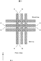
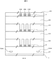
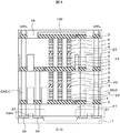
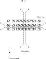
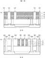
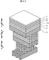
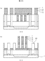
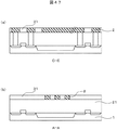
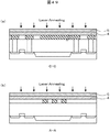
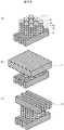
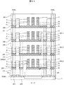
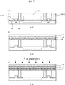
図1は、本発明の実施例1である半導体記憶装置の一例を示した一部平面であり、図2〜5は、それぞれ図1におけるA−A線、B−B線、C−C線、D−D線断面図である。また図6は、メモリアレイ部分だけを示した立体図である。なお、図1の平面図、図6の立体図において、図面を見やすくするために一部の部材は省略している。
FIG. 1 is a partial plan view showing an example of a semiconductor memory device that is
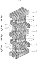
本実施例の半導体記憶装置は、メモリ素子に抵抗可変素子(例えば、相変化メモリ)、選択素子にポリシリコンダイオードを用いていて、これらが積層クロスポイント型にアレイを構成している。半導体主面内のx方向にワード線、y方向にビット線が延在しており、それぞれアレイ端のコンタクト孔を介して選択トランジスタSTの拡散層に接続されている。選択トランジスタの他方の拡散層はコンタクト孔を介してグローバルワード線GWL、グローバルビット線GBLに接続されている。隣接するメモリ層はビット線かワード線のいずれかを共用する構造になっていて、これを実現するために選択素子となるダイオードの極性は隣接メモリ層で逆向きである(図6)。図1から図6では4層積層の場合のメモリアレイを示しているが、5層以上を積層することももちろん可能である。 In the semiconductor memory device of this embodiment, a variable resistance element (for example, a phase change memory) is used as a memory element, and a polysilicon diode is used as a selection element, and these constitute a stacked cross point type array. A word line extends in the x direction and a bit line extends in the y direction in the semiconductor main surface, and each is connected to the diffusion layer of the select transistor ST via a contact hole at the end of the array. The other diffusion layer of the selection transistor is connected to the global word line GWL and the global bit line GBL through contact holes. Adjacent memory layers are structured to share either bit lines or word lines, and in order to realize this, the polarity of the diode that becomes the selection element is opposite in the adjacent memory layers (FIG. 6). 1 to 6 show a memory array in the case of four-layer stacking, it is of course possible to stack five or more layers.
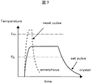
相変化メモリは、Ge2Sb2Te5などの相変化材料がアモルファス状態と結晶状態で抵抗値が異なることを利用して情報を記憶する。アモルファス状態では抵抗が高く、結晶状態では抵抗が低い。したがって、読み出しは素子の両端に電位差を与え、素子に流れる電流を測定することで、素子の高抵抗状態/低抵抗状態を判別することで行える。 The phase change memory stores information using the fact that phase change materials such as Ge 2 Sb 2 Te 5 have different resistance values between an amorphous state and a crystalline state. The resistance is high in the amorphous state and low in the crystalline state. Therefore, reading can be performed by determining a high resistance state / low resistance state of the element by applying a potential difference to both ends of the element and measuring a current flowing through the element.
相変化材料を高抵抗のアモルファス状態から低抵抗の結晶状態に変化させる動作、逆に低抵抗の結晶状態から高抵抗のアモルファス状態に変化させる動作は、図7のような温度変化を相変化材料に与えることで行える。アモルファス状態の相変化材料は結晶化温度以上に加熱し10−6秒程度以上保持することで結晶状態にすることができる。また、結晶状態の相変化材料は、融点以上の温度まで加熱し液体状態にした後、急速に冷却することでアモルファス状態にすることができる。 The operation of changing the phase change material from the high-resistance amorphous state to the low-resistance crystalline state, and conversely the operation of changing the low-resistance crystal state to the high-resistance amorphous state is performed by changing the temperature change as shown in FIG. This can be done by giving The phase change material in an amorphous state can be brought into a crystalline state by heating to a temperature above the crystallization temperature and holding it for about 10 −6 seconds or more. Further, the phase change material in a crystalline state can be brought into an amorphous state by heating it to a temperature equal to or higher than the melting point to make it liquid and then rapidly cooling it.
相変化メモリでは電流により発生するジュール熱によって、相変化膜の電気抵抗を異なる状態に変化させることによりデータ書き込み行う。リセット動作、すなわち高抵抗のアモルファス状態へ変化させる動作は、大電流を短時間流して溶解させた後、電流を急減させ急冷することにより行う。一方、セット動作、すなわち低抵抗の結晶状態へ変化させる動作は、結晶化温度に保持するのに十分な電流を長時間流すことにより行う。 In the phase change memory, data is written by changing the electric resistance of the phase change film to different states by Joule heat generated by current. The reset operation, that is, the operation of changing to the high resistance amorphous state is performed by flowing a large current for a short time and dissolving it, and then rapidly decreasing and rapidly cooling the current. On the other hand, the set operation, that is, the operation of changing to a low-resistance crystal state is performed by flowing a current sufficient for maintaining the crystallization temperature for a long time.
図8の等価回路図を用いて、本実施例の半導体装置の読出し動作を説明する。メモリアレイ中から1セルを選択して読出しを行なうには、選択セルが接続されているワード線(SWL:選択ワード線)、選択セルが接続されていないワード線(USWL:非選択ワード線)、選択セルが接続されているビット線(SBL:選択ビット線)、選択セルが接続されていないビット線(USBL:非選択ビット線)に、例えばそれぞれ、1V、0V、0V、1Vの電圧を印加する。ダイオードが逆向き電圧のリーク電流をほとんど流さないおかげで、選択セルSMCだけに電流が流れ、センスアンプで測定することで抵抗状態を判定できる。 The read operation of the semiconductor device of this embodiment will be described with reference to the equivalent circuit diagram of FIG. To select and read one cell from the memory array, the word line to which the selected cell is connected (SWL: selected word line) and the word line to which the selected cell is not connected (USWL: unselected word line) For example, voltages of 1V, 0V, 0V, and 1V are applied to the bit line to which the selected cell is connected (SBL: selected bit line) and the bit line to which the selected cell is not connected (USBL: unselected bit line), respectively. Apply. Thanks to the fact that the diode hardly allows the reverse voltage leakage current to flow, the current flows only in the selected cell SMC, and the resistance state can be determined by measuring with the sense amplifier.
図9の等価回路図を用いて、本実施例の半導体装置のセット/リセット動作を説明する。メモリアレイ中から1セルを選択してセット動作を行うには、選択セルが接続されているワード線(SWL:選択ワード線)、選択セルが接続されていないワード線(USWL:非選択ワード線)、選択セルが接続されているビット線(SBL:選択ビット線)、選択セルが接続されていないビット線(USBL:非選択ビット線)に例えばそれぞれ、2.5V、0V、0V、2.5Vの電圧を印加する。この時、非選択ワード線、非選択ビット線に接続されたCellDは、ダイオードに印加される電圧が逆方向電圧であるために電流が流れない。また、選択ワード線、非選択ビット線に接続されたCellB,非選択ワード線、選択ビット線に接続されたCellDはビット線とワード線が等電位であるために電流が流れない。選択セルSMCにだけ電流が流れジュール熱により相変化材料が加熱される。選択ビット線、選択ワード線に印加する電圧は選択メモリセルの相変化材料を結晶化温度に加熱するのに充分な電圧であれば良い。結晶化に充分な時間(10−6秒程度以上)電圧を印加すると、選択セルの相変化素子は低抵抗の結晶状態になり、それ以外のセルは状態を変化させない。 The set / reset operation of the semiconductor device of this embodiment will be described with reference to the equivalent circuit diagram of FIG. To select one cell from the memory array and perform the set operation, the word line to which the selected cell is connected (SWL: selected word line), the word line to which the selected cell is not connected (USWL: unselected word line) ), For example, 2.5V, 0V, 0V, 2) to the bit line to which the selected cell is connected (SBL: selected bit line) and the bit line to which the selected cell is not connected (USBL: unselected bit line), respectively. Apply a voltage of 5V. At this time, no current flows through CellD connected to the unselected word line and unselected bit line because the voltage applied to the diode is a reverse voltage. In addition, no current flows through the selected word line, Cell B connected to the non-selected bit line, and Cell D connected to the non-selected word line and the selected bit line because the bit line and the word line are equipotential. A current flows only in the selected cell SMC, and the phase change material is heated by Joule heat. The voltage applied to the selected bit line and the selected word line may be a voltage sufficient to heat the phase change material of the selected memory cell to the crystallization temperature. When a voltage is applied for a sufficient time for crystallization (about 10 −6 seconds or more), the phase change element of the selected cell becomes a low resistance crystal state, and the other cells do not change the state.
メモリアレイ中から1セルを選択してリセット動作を行うには、選択セルが接続されているワード線(SWL:選択ワード線)、選択セルが接続されていないワード線(USWL:非選択ワード線)、選択セルが接続されているビット線(SBL:選択ビット線)、選択セルが接続されていないビット線(USBL:非選択ビット線)に例えばそれぞれ、3V、0V、3V、0Vの電圧を印加する。この時、非選択ワード線、非選択ビット線に接続されたCellDは、ダイオードに印加される電圧が逆方向電圧であるために電流が流れない。また、選択ワード線、非選択ビット線に接続されたCellB,非選択ワード線、選択ビット線に接続されたCellDはビット線とワード線が等電位であるために電流が流れない。選択セルSMCにだけ電流が流れジュール熱により相変化材料が加熱される。選択ビット線、選択ワード線に印加する電圧は選択メモリセルの相変化材料を融点以上の温度に加熱するのに充分な電圧であれば良い。印加電圧を急速に0にし相変化材料を急冷すると選択セルの相変化素子は高抵抗のアモルファス状態になり、それ以外のセルは状態を変化させない。 To select one cell from the memory array and perform a reset operation, the word line to which the selected cell is connected (SWL: selected word line), the word line to which the selected cell is not connected (USWL: unselected word line) ) For example, 3V, 0V, 3V, and 0V are applied to the bit line to which the selected cell is connected (SBL: selected bit line) and the bit line to which the selected cell is not connected (USBL: unselected bit line), respectively. Apply. At this time, no current flows through CellD connected to the unselected word line and unselected bit line because the voltage applied to the diode is a reverse voltage. In addition, no current flows through the selected word line, Cell B connected to the non-selected bit line, and Cell D connected to the non-selected word line and the selected bit line because the bit line and the word line are equipotential. A current flows only in the selected cell SMC, and the phase change material is heated by Joule heat. The voltage applied to the selected bit line and the selected word line may be a voltage sufficient to heat the phase change material of the selected memory cell to a temperature higher than the melting point. When the applied voltage is rapidly reduced to 0 and the phase change material is rapidly cooled, the phase change element of the selected cell becomes a high resistance amorphous state, and the other cells do not change the state.
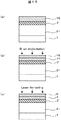
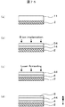
次に、図10〜図34を用いて上記積層相変化メモリの製造方法を説明する。
まず、シリコン基板上に公知の技術を用いて図2のA−A断面、図4のC−C断面に見られる選択トランジスタSTを形成する。メモリアレイの駆動に必要な周辺回路を形成するシリコン基板上のデバイスに関しても同様に形成する。
ST形成後に絶縁膜21でSTおよび、周辺回路のデバイスを埋め込み、必要に応じて化学的機械研磨法(CMP法)などで表面を平坦化、更にこの後形成するメモリアレイのワード線2とSTの拡散層Difを接続するCONTを形成したのが図10(a)の状態である。次にワード線となる例えばタングステン2、Bドープアモルファスシリコン14、不純物をドープしないアモルファスシリコン11を成膜する(図10(b))。タングステン膜2の成膜にはスパッタ法、Bドープアモルファスシリコン14、不純物をドープしないアモルファスシリコン11の成膜にはCVD法を用いた。タングステン成膜温度は200℃以下、Bドープアモルファスシリコンの成膜温度は400℃程度、不純物をドープしないアモルファスシリコン11の成膜温度は530℃程度である。次に、イオン打ち込み法によりリンイオンをアモルファスシリコン11にドープする(図10(c))。
Next, the manufacturing method of the said laminated phase change memory is demonstrated using FIGS.
First, a selection transistor ST as seen in the AA cross section of FIG. 2 and the CC cross section of FIG. 4 is formed on a silicon substrate using a known technique. A device on a silicon substrate for forming a peripheral circuit necessary for driving the memory array is similarly formed.
After forming ST, ST and peripheral circuit devices are embedded in the insulating
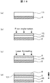
次に、例えばCO2レーザーアニールにより、アモルファスシリコン14、15を結晶化し不純物の活性化も行う(図11(a))。この時点では、相変化メモリ材料は含まれていないので、熱負荷低減の目的で行うレーザーアニールは必須ではなく、通常の加熱炉によるポリシリコンの結晶化、不純物の活性化を行うことも可能であるが、後述するように2層目以降のメモリアレイを製造する際には、レーザーアニールが必須である。本実施例では、1層目と2層目以降の選択素子の特性を同等にそろえるために、図11(a)の工程で2層目以降に用いるのと同じレーザーアニールを用いた。
Next, the
次に、WSi、TiSi2などのシリサイド10をPドープポリシリコン5の表面に形成し、相変化素子の下部電極となる8(TiN、Wなど)、相変化材料6(Ge2Sb2Te5など)、相変化素子の上部電極となる7(TiN、Wなど)を順に成膜した(図62(b))。
ポリシリコン積層ダイオード構造は、図10、11に示した方法以外の方法でも形成できる。
Next, a
The polysilicon multilayer diode structure can be formed by a method other than the method shown in FIGS.
別方法の1つ目は、図12(a)(b)に示す以下の方法である。
ワード線となる例えばタングステン2、Bドープアモルファスシリコン14、Pをドープしたアモルファスシリコン15を成膜する(図12(a))。タングステン膜2の成膜にはスパッタ法、Bドープアモルファスシリコン14、Pをドープしたアモルファスシリコン15の成膜にはCVD法を用いた。タングステン成膜温度は200℃以下、Bドープアモルファスシリコンの成膜温度は400℃程度、Pをドープしたアモルファスシリコン15の成膜温度は530℃程度である。次に、例えばCO2レーザーアニールにより、アモルファスシリコン14、15を結晶化し不純物の活性化も行う(図12(b))。
別方法の2つ目は、図12(c)(d)に示す以下の方法である。
ワード線となる、例えばタングステン2、Bドープアモルファスシリコン14、不純物をドープしないアモルファスシリコン11、Pをドープしたアモルファスシリコン15を成膜する(図12(c))。タングステン膜2の成膜にはスパッタ法、Bドープアモルファスシリコン14、不純物をドープしないアモルファスシリコン11、Pをドープしたアモルファスシリコン15の成膜にはCVD法を用いた。タングステン成膜温度は200℃以下、Bドープアモルファスシリコンの成膜温度は400℃程度、不純物をドープしないアモルファスシリコン11、Pをドープしたアモルファスシリコン15の成膜温度は530℃程度である。次に、例えばCO2レーザーアニールにより、アモルファスシリコン14、11、15を結晶化し不純物の活性化も行う(図12(d))。
The first of the other methods is the following method shown in FIGS.
For example,
The second of the other methods is the following method shown in FIGS.
For example,
別方法の3つ目は、図13(a)〜(d)に示す以下の方法である。
ワード線となる例えばタングステン2、不純物をドープしないアモルファスシリコン11を成膜する(図13(a))。タングステン膜2の成膜にはスパッタ法、不純物をドープしないアモルファスシリコン11の成膜にはCVD法を用いた。タングステン成膜温度は200℃以下、不純物をドープしないアモルファスシリコン11の成膜温度は530℃程度である。次に、イオン打ち込み法によりBイオンをアモルファスシリコン11の下半分に最大濃度が入るようにドープする(図13(b))。次に、イオン打ち込み法によりPイオンをアモルファスシリコン11の上半分に最大濃度が入るようにドープする(図13(c))。次に例えばCO2レーザーアニールにより、アモルファスシリコン14、15を結晶化し不純物の活性化も行う(図13(d))。
The third of the other methods is the following method shown in FIGS.
For example,
別方法の4つ目は、図14(a)〜(c)に示す以下の方法である。
ワード線となる例えばタングステン2、Bをドープしたアモルファスシリコン14を成膜する(図14(a))。タングステン膜2の成膜にはスパッタ法、Bをドープしたアモルファスシリコン14の成膜にはCVD法を用いた。タングステン成膜温度は200℃以下、Bをドープしたアモルファスシリコン14の成膜温度は400℃程度である。次に、イオン打ち込み法によりPイオンをアモルファスシリコン11の上半分に最大濃度が入るようにドープする(図14(b))。次に例えばCO2レーザーアニールにより、アモルファスシリコン14、15を結晶化し不純物の活性化も行う(図14(c))。
別方法の5つ目は、図15(a)〜(c)に示す以下の方法である。ワード線となる例えばタングステン2、Pをドープしたアモルファスシリコン15を成膜する(図15(a))。タングステン膜2の成膜にはスパッタ法、Pをドープしたアモルファスシリコン15の成膜にはCVD法を用いた。タングステン成膜温度は200℃以下、Pをドープしたアモルファスシリコン15の成膜温度は530℃程度である。次に、イオン打ち込み法によりBイオンをアモルファスシリコン11の下半分に最大濃度が入るようにドープする(図15(b))。次に、例えばCO2レーザーアニールにより、アモルファスシリコン14、15を結晶化し不純物の活性化も行う(図15(c))。
The fourth of the other methods is the following method shown in FIGS.
The fifth of the other methods is the following method shown in FIGS.
図11(b)の次に、上部電極材料7、相変化材料6、下部電極材料8、シリサイド膜10、Pドープポリシリコン5、Bドープポリシリコン4、ワード線材料2をx方向に延在するストライプ状にパターニングした。この時、WL、GWLに至るコンタクト孔が形成される部分にはパターンを残す(図16(a))。この工程でのA−A断面を示したのが図16(b)である。パターンの平面図は図17である。またメモリアレイ部分の立体図は図18となる。
Next to FIG. 11B, the
次に、シリコン酸化膜22を例えばCVD法で堆積し、図16でパターニングしたスペースが完全に埋まり込むようにする。次に、例えばCMP法で表面を平坦化し上部電極7を露出させ、ビット線と選択トランジスタの拡散層を接続するためのコンタクト孔150を形成する(図19(a)(b))。
Next, a
次に、例えば孔150内に例えばCVD法でW、またはTi、TiN、Wを順に埋め込む。上表面に堆積したWを例えばCMP法で除去することでplugを形成する。次にビット線3となる材料(例えばタングステン)を成膜し、TiNなどのバリアメタル、またはWSi、TiSi2などのシリサイド膜、またバリアメタルとシリサイド膜を順に成膜した膜10を形成し、Pをドープしたアモルファスシリコン15を成膜する。次に、不純物をドープしないアモルファスシリコン11を成膜する(図20(a))。
次に、イオン打ち込み法によりBイオンをアモルファスシリコン11にドープする(図20(b))。
Next, for example, W or Ti, TiN, and W are sequentially buried in the
Next, B ions are doped into the
次に、例えばCO2レーザーアニールにより、アモルファスシリコン14、15を結晶化し不純物の活性化も行う(図21(a))。
レーザーアニールは、アモルファスシリコンの結晶化と不純物の活性化を充分に行い、選択素子となるダイオードの電流駆動能力を充分なものにすること、1層目のメモリアレイを構成する相変化メモリ材料6への熱負荷を低減し歩留りを低下させないことを目的に行う。
Next, the
The laser annealing sufficiently crystallizes the amorphous silicon and activates the impurities so that the current drive capability of the diode serving as the selection element is sufficient, and the phase
通常、炉体によるポリシリコンの結晶化には700℃以上の長時間熱処理が必要であり、この熱負荷で相変化素子の歩留りはほぼ0%にまで低下してしまう。相変化材料6と結晶化を行う2層目のアモルファスシリコンの間に、ビット線材料3が存在する状態で、レーザーアニールによる短時間アニールを行なうと、炉対加熱の場合と比較して、2層目のアモルファスシリコンを結晶化する際の相変化材料6の温度上昇を抑制でき熱負荷を低減できる。
Usually, a long time heat treatment of 700 ° C. or more is required for crystallization of polysilicon by a furnace body, and the yield of the phase change element is reduced to almost 0% by this heat load. When annealing is performed for a short time by laser annealing in the state where the
次に、WSi、TiSi2などのシリサイド9をBドープポリシリコン4の表面に形成し、相変化素子の下部電極となる8(TiN、Wなど)、相変化材料6(Ge2Sb2Te5など)、相変化素子の上部電極となる7(TiN、Wなど)を順に成膜した(図21(b))。
ポリシリコンによる積層PNダイオード構造は、図72〜74に示した方法以外の方法でも形成できる。
Next, a
The stacked PN diode structure made of polysilicon can be formed by a method other than the method shown in FIGS.
別方法の1つ目は、図22(a)(b)に示す以下の方法である。ビット線となる例えばタングステン3、TiNなどのバリアメタル、またはWSi、TiSi2などのシリサイド膜、またバリアメタルとシリサイド膜を順に成膜した膜10を形成し、Pドープアモルファスシリコン15、Bドープしたアモルファスシリコン14を成膜する(図22(a))。タングステン膜3の成膜にはスパッタ法、Bドープアモルファスシリコン14、Pをドープしたアモルファスシリコン15の成膜にはCVD法を用いた。タングステン成膜温度は200℃以下、Bドープアモルファスシリコンの成膜温度は400℃程度、Pをドープしたアモルファスシリコン15の成膜温度は530℃程度である。次に例えばCO2レーザーアニールにより、アモルファスシリコン14、15を結晶化し不純物の活性化も行う(図22(b))。
The first of the other methods is the following method shown in FIGS. 22 (a) and 22 (b). For example, a barrier metal such as
別方法の2つ目は、図22(c)(d)に示す以下の方法である。ビット線となる例えばタングステン3、TiNなどのバリアメタル、またはWSi、TiSi2などのシリサイド膜、またバリアメタルとシリサイド膜を順に成膜した膜10を形成し、Pドープアモルファスシリコン15、不純物をドープしないアモルファスシリコン11、Bドープアモルファスシリコン14を成膜する(図22(c))。タングステン膜3の成膜にはスパッタ法、Bドープアモルファスシリコン14、不純物をドープしないアモルファスシリコン11、Pドープアモルファスシリコン15の成膜にはCVD法を用いた。タングステン成膜温度は200℃以下、Bドープアモルファスシリコンの成膜温度は400℃程度、不純物をドープしないアモルファスシリコン11、Pドープアモルファスシリコン15の成膜温度は530℃程度である。次に例えばCO2レーザーアニールにより、アモルファスシリコン14、11、15を結晶化し不純物の活性化も行う(図22(d))。
The second of the other methods is the following method shown in FIGS. For example, a barrier metal such as
別方法の3つ目は、図23(a)〜(d)に示す以下の方法である。ビット線となる例えばタングステン3、TiNなどのバリアメタル、またはWSi、TiSi2などのシリサイド膜、またバリアメタルとシリサイド膜を順に成膜した膜10を形成し、不純物をドープしないアモルファスシリコン11を成膜する(図23(a))。タングステン膜3の成膜にはスパッタ法、不純物をドープしないアモルファスシリコン11の成膜にはCVD法を用いた。タングステン成膜温度は200℃以下、不純物をドープしないアモルファスシリコン11の成膜温度は530℃程度である。次に、イオン打ち込み法によりBイオンをアモルファスシリコン11の上半分に最大濃度が入るようにドープする(図23(b))。次に、イオン打ち込み法によりPイオンをアモルファスシリコン11の下半分に最大濃度が入るようにドープする(図23(c))。次に例えばCO2レーザーアニールにより、アモルファスシリコン14、15を結晶化し不純物の活性化も行う(図23(d))。
The third of the other methods is the following method shown in FIGS. For example, a barrier metal such as
別方法の4つ目は、図24(a)〜(c)に示す以下の方法である。ビット線となる例えばタングステン3、TiNなどのバリアメタル、またはWSi、TiSi2などのシリサイド膜、またバリアメタルとシリサイド膜を順に成膜した膜10を形成し、Bドープアモルファスシリコン14を成膜する(図24(a))。タングステン膜3の成膜にはスパッタ法、Bドープアモルファスシリコン14の成膜にはCVD法を用いた。タングステン成膜温度は200℃以下、Bドープアモルファスシリコン14の成膜温度は400℃程度である。次に、イオン打ち込み法によりPイオンをアモルファスシリコン11の下半分に最大濃度が入るようにドープする(図24(b))。次に例えばCO2レーザーアニールにより、アモルファスシリコン14、15を結晶化し不純物の活性化も行う(図24(c))。
The fourth of the other methods is the following method shown in FIGS. For example, a barrier metal such as
別方法の5つ目は、図25(a)〜(c)に示す以下の方法である。ビット線となる例えばタングステン3、Pをドープしたアモルファスシリコン15を成膜する(図25(a))。タングステン膜3の成膜にはスパッタ法、Pドープアモルファスシリコン15の成膜にはCVD法を用いた。タングステン成膜温度は200℃以下、Pドープアモルファスシリコン15の成膜温度は530℃程度である。次に、イオン打ち込み法によりBイオンをアモルファスシリコン11の上半分に最大濃度が入るようにドープする(図25(b))。次に例えばCO2レーザーアニールにより、アモルファスシリコン14、15を結晶化し不純物の活性化も行う(図25(c))。
The fifth of the other methods is the following method shown in FIGS.
図21(b)の次に、上部電極材料7、相変化材料6、下部電極材料8、シリサイド膜9、Bドープポリシリコン4、Pドープポリシリコン5、TiNなどのバリアメタル、またはWSi、TiSi2などのシリサイド膜、またバリアメタルとシリサイド膜を順に成膜した膜10を形成し、ビット線材料3、1層目のメモリアレイの上部電極7、1層目のメモリアレイの相変化材料6、1層目のメモリアレイの下部電極8、1層目のメモリアレイの膜10、1層目のメモリアレイのPドープポリシリコン5、1層目のメモリアレイのBドープポリシリコン4をy方向に延在するストライプ状にパターニングした。この時、BL、GBLに至るコンタクト孔が形成される部分にはパターンを残す(図26(a))。この工程でのC−C断面を示したのが図26(b)である。パターンの平面図は図27である。またメモリアレイ部分の立体図は図28(a)がパターニングされて図28(b)となる。2層目のメモリアレイがストライプ状にパターニングされ、1層目のメモリアレイのクロスポイント構造が完成する。
Next to FIG. 21B, the
次にシリコン酸化膜23を例えばCVD法で堆積し、図26でパターニングしたスペースが完全に埋まり込むようにし、例えばCMP法で表面を平坦化し上部電極7を露出させ、ワード線1層目のパターンに至るコンタクト孔150を形成、その後、例えば孔150内に例えばCVD法でWを埋め込む。上表面に堆積したWを例えばCMP法で除去することでplugを形成した。次にワード線となる例えばタングステン2、Bドープアモルファスシリコン14、不純物をドープしないアモルファスシリコン11を成膜する(図29(a))。タングステン膜2の成膜にはスパッタ法、Bドープアモルファスシリコン14、不純物をドープしないアモルファスシリコン11の成膜にはCVD法を用いた。タングステン成膜温度は200℃以下、Bドープアモルファスシリコンの成膜温度は400℃程度、不純物をドープしないアモルファスシリコン11の成膜温度は530℃程度である。次に、イオン打ち込み法によりリンイオンをアモルファスシリコン11にドープする。次に例えばCO2レーザーアニールにより、アモルファスシリコン14、15を結晶化し不純物の活性化も行う(図29(b))。
Next, a
次に、TiNなどのバリアメタル、またはWSi、TiSi2などのシリサイド膜10をPドープポリシリコン5の表面に形成し、相変化素子の下部電極となる8(TiN、Wなど)、相変化材料6(Ge2Sb2Te5など)、相変化素子の上部電極となる7(TiN、Wなど)を順に成膜した(図30)。
Next, a barrier metal such as TiN or a
ポリシリコンによる積層PNダイオード構造は、図29に示した方法以外の方法でも形成できる。前述のように、別方法1(図22(a)(b))、別方法2(図22(c)(d))、別方法3(図23(a)〜(d))、別方法4(図24(a)〜(c))、別方法5(図25(a)〜(c))を用いることもできる。 The stacked PN diode structure made of polysilicon can be formed by a method other than the method shown in FIG. As described above, Alternative Method 1 (FIGS. 22A and 22B), Alternative Method 2 (FIGS. 22C and 22D), Alternative Method 3 (FIGS. 23A to 23D), Alternative Method 4 (FIGS. 24A to 24C) and another method 5 (FIGS. 25A to 25C) can also be used.
次に、上部電極材料7、相変化材料6、下部電極材料8、シリサイド膜10、Pドープポリシリコン5、Bドープポリシリコン4、ワード線材料2、2層目のメモリアレイの上部電極7、2層目のメモリアレイの相変化材料6、2層目のメモリアレイの下部電極8、2層目のメモリアレイのシリサイド9、2層目のメモリアレイのBドープポリシリコン4、2層目のメモリアレイのPドープポリシリコン5をx方向に延在するストライプ状にパターニングした。またメモリアレイ部分の立体図は図31となる。3層目のメモリアレイがストライプ状にパターニングされ、2層目のメモリアレイのクロスポイント構造が完成する。
Next, the
以下、同様のプロセスを繰り返すことで、本実施例の4層積層クロスポイントメモリを完成することができる。
図30の次にシリコン酸化膜24を例えばCVD法で堆積し、図88、89でパターニングしたスペースが完全に埋まり込むようにする。次に、例えばCMP法で表面を平坦化し上部電極7を露出させる。次に、ビット線に接続する選択トランジスタの拡散層に至るコンタクト孔を形成した後、例えばCVD法で孔内にWを埋め込み上表面に堆積したWをCMP法で除去することでplugを形成する。次に2層目のメモリアレイと同様の工程で、ビット線3、バリアメタル膜またはシリサイド膜10を形成、Pドープポリシリコン、Bドープポリシリコン、シリサイド9、下部電極8、相変化材料6、上部電極7の積層構造を形成する(図32)。
Thereafter, the same process is repeated to complete the four-layer stacked cross point memory of this embodiment.
Next to FIG. 30, a
次に、上部電極材料7、相変化材料6、下部電極材料8、シリサイド膜9、Bドープポリシリコン4、Pドープポリシリコン5、バリアメタル膜またはシリサイド膜10、ビット線材料3、3層目のメモリアレイの上部電極7、3層目のメモリアレイの相変化材料6、3層目のメモリアレイの下部電極8、3層目のメモリアレイのバリアメタル膜またはシリサイド膜10、3層目のメモリアレイのPドープポリシリコン5、3層目のメモリアレイのBドープポリシリコン4をy方向に延在するストライプ状にパターニングした(図33)。4層目のメモリアレイがストライプ状にパターニングされ、3層目のメモリアレイのクロスポイント構造が完成する。
Next,
次にシリコン酸化膜25を例えばCVD法で堆積し、図33でパターニングしたスペースが完全に埋まり込むようにする。次に、例えばCMP法で表面を平坦化し上部電極7を露出させた後、ワード線2層目のパターンに至るコンタクト孔を形成した後、孔内に例えばCVD法でWを埋め込み上表面に堆積したWをCMP法で除去することでplugを形成する。次にワード線となる例えばタングステン2、ハードマスクとなる例えばシリコン酸化膜30を成膜する(図34)。
Next, a
次に、ハードマスク30、ワード線材料2、上部電極7、相変化材料6、下部電極8、シリサイド9、Bドープポリシリコン4、Pドープポリシリコン5をx方向に延在するストライプ状にパターニングした。
次にシリコン酸化膜26を例えばCVD法で堆積し、図34でパターニングしたスペースが完全に埋まり込むようにした後、例えばCMP法で表面を平坦化する。その後、最上層のワード線パターン、ビット線パターンと、GWL、GBLを接続するためのプラグを形成した。この後、図には示していないが、選択トランジスタSTのウェル、ゲートに給電するための配線、GBL、GWLを形成し半導体記憶装置を完成した。
Next, the
Next, a
長時間の炉体加熱により選択素子となるトランジスタのポリシリコン結晶化を行う従来の方法で製造すると、積層相変化メモリの選択素子の電流駆動能力と相変化素子の歩留りYmin以上を両立させることが不可能であった(図36(a))。Yminは、相変化メモリの積層化によるコスト低減を可能とするための最小歩留り値である。本発明の方法で両立させることが可能となり、積層化による相変化メモリの低コスト大容量化が可能となった(図36(b))。 When manufactured by a conventional method of crystallizing a transistor that becomes a selection element by heating the furnace body for a long time, the current driving capability of the selection element of the stacked phase change memory and the yield Ymin of the phase change element can be made compatible. It was impossible (FIG. 36 (a)). Ymin is a minimum yield value for enabling cost reduction by stacking phase change memories. The method of the present invention makes it possible to achieve both, and it is possible to increase the cost and capacity of the phase change memory by stacking (FIG. 36B).
本実施例1では、抵抗可変素子を相変化メモリ、選択素子となるトランジスタをポリシリコンで形成したが、抵抗可変素子をNiO、CuO、TiO2などのReRAM、選択トランジスタをGe、SiGeなどのシリコン以外の半導体を用いることも可能であり、同様の効果を得ることができた。 In the first embodiment, the variable resistance element is formed of phase change memory, and the transistor serving as the selection element is formed of polysilicon. However, the variable resistance element is formed of ReRAM such as NiO, CuO, and TiO 2, and the selection transistor is formed of silicon such as Ge and SiGe. Other semiconductors can be used, and the same effect can be obtained.
実施例1では、レーザーアニールによるアモルファスシリコンの結晶化、不純物の活性化を行う際に、アモルファスシリコン直下のワード線材料、またはビット線材料が半導体主面全体を覆っていたが、本実施例2のようにレーザーアニールの際にワード線材料、ビット線材料が半導体主面の全てを覆わない製造方法も可能である。
本実施例2の半導体記憶装置の製造方法を図37〜図46に示す。
In the first embodiment, when crystallizing amorphous silicon by laser annealing and activating impurities, the word line material or bit line material directly under the amorphous silicon covers the entire semiconductor main surface. Thus, a manufacturing method in which the word line material and the bit line material do not cover the entire semiconductor main surface during laser annealing is also possible.
A method of manufacturing the semiconductor memory device according to the second embodiment is shown in FIGS.
まず、実施例1と同様に選択トランジスタおよび周辺回路デバイスを半導体基板1上に形成し、絶縁膜21を形成する。次にワード線材料(例えばW)をスパッタ法で成膜する。タングステン成膜温度は200℃以下である。次に、ワード線材料をパターニングし、図37(a)(b)(c)のようにする。
First, similarly to the first embodiment, the selection transistor and the peripheral circuit device are formed on the
次に、Bドープアモルファスシリコン14、不純物をドープしないアモルファスシリコン11を成膜する(図38(a))。Bドープアモルファスシリコン14、不純物をドープしないアモルファスシリコン11の成膜にはCVD法を用いた。Bドープアモルファスシリコンの成膜温度は400℃程度、不純物をドープしないアモルファスシリコン11の成膜温度は530℃程度である。
Next, B-doped
次に、イオン打ち込み法によりリンイオンをアモルファスシリコン11にドープした後、次に、例えばCO2レーザーアニールにより、アモルファスシリコン14、15を結晶化し不純物の活性化も行う(図39(a)(b))。この時点では、相変化メモリ材料は含まれていないので、熱負荷低減の目的で行うレーザーアニールは必須ではなく、通常の加熱炉によるポリシリコンの結晶化、不純物の活性化を行うことも可能であるが、後述するように2層目以降のメモリアレイを製造する際には、レーザーアニールが必須である。本実施例では、1層目と2層目以降の選択素子の特性を同等にそろえるために、2層目以降のダイオードを形成するポリシリコンの結晶化と同様のレーザーアニールを用いた。
Next, after doping phosphorus ions into the
レーザーアニールによるアモルファスシリコンの結晶化の際には、レーザーを半導体主面の全体に同時に照射するのではなく、部分に分けて照射する。この際、金属膜であるワード線材料2が半導体主面全体で繋がっていると、レーザー照射部の熱がワード線材料2を伝わって放熱するため、結晶化のために大きなレーザーパワーが必要になる。本実施例2のように結晶化を行うアモルファスシリコン直下の金属膜をパターニングすることで、少ないレーザーパワーでアモルファスシリコンの結晶化、不純物の活性化が可能となる。
When amorphous silicon is crystallized by laser annealing, the laser is not irradiated to the entire semiconductor main surface at the same time, but is divided into portions. At this time, if the
次に、WSi、TiSi2などのシリサイド10をPドープポリシリコン5の表面に形成し、相変化素子の下部電極となる8(TiN、Wなど)、相変化材料6(Ge2Sb2Te5など)、相変化素子の上部電極となる7(TiN、Wなど)を順に成膜した。ポリシリコンによる積層PNダイオード構造は、図38から39に示した方法以外の方法でも形成できる。
Next, a
実施例1に示した、別方法1(図12(a)(b))、別方法2(図12(c)(d))、別方法3(図13(a)〜(d))、別方法4(図14(a)〜(c))、別方法5(図15(a)〜(c))をパターニングしたワード線2上で用いることもできる。
次に、上部電極材料7、相変化材料6、下部電極材料8、シリサイド膜10、Pドープポリシリコン5、Bドープポリシリコン4、ワード線材料2をx方向に延在するストライプ状にパターニングした。平面図は、図41(a)が図41(b)となる。この時、WL、GWLに至るコンタクト孔が形成される部分にはパターンを残す。
Alternative method 1 (FIGS. 12A and 12B), alternative method 2 (FIGS. 12C and 12D), alternative method 3 (FIGS. 13A to 13D) shown in Example 1, Alternative method 4 (FIGS. 14A to 14C) and alternative method 5 (FIGS. 15A to 15C) can also be used on the
Next, the
次に、シリコン酸化膜22を例えばCVD法で堆積し、図40(a)(b)でパターニングしたスペースが完全に埋まり込むようにする。次に、例えばCMP法で表面を平坦化し上部電極7を露出させ、ビット線と選択トランジスタの拡散層を接続するためのコンタクト孔を形成する。次に例えばコンタクト孔内に例えばCVD法でW、またはTi、TiN、Wを順に埋め込む。上表面に堆積したWを例えばCMP法で除去することでplugを形成した後、ビット線材料3を成膜する(図121(a)(b))。
Next, a
次に、ビット線材料をパターニングし、図42、図43(a)(b)のようにする。
次に、Wsi、TiSi2などのシリサイド膜10を形成、Pをドープしたアモルファスシリコン15、不純物をドープしないアモルファスシリコン11を成膜する。次に、イオン打ち込み法によりBイオンをアモルファスシリコン11にドープした後、例えばCO2レーザーアニールにより、アモルファスシリコン14、15を結晶化し不純物の活性化も行う(図44(a)(b))。
Next, the bit line material is patterned as shown in FIGS. 42, 43 (a) and 43 (b).
Next, a
レーザーアニールは、アモルファスシリコンの結晶化と不純物の活性化を充分に行い、選択素子となるダイオードの電流駆動能力を充分なものにすること、1層目のメモリアレイを構成する相変化メモリ材料6への熱負荷を低減し歩留りを低下させないことを目的に行う。
The laser annealing sufficiently crystallizes the amorphous silicon and activates the impurities so that the current drive capability of the diode serving as the selection element is sufficient, and the phase
通常、炉体によるポリシリコンの結晶化には700℃以上の長時間熱処理が必要であり、この熱負荷で相変化素子の歩留りはほぼ0%にまで低下してしまう。相変化材料6と結晶化を行う2層目のアモルファスシリコンの間に、ビット線材料3が存在する状態で、レーザーアニールによる短時間アニールを行なうと、炉対加熱の場合と比較して、2層目のアモルファスシリコンを結晶化する際の相変化材料6の温度上昇を抑制でき熱負荷を低減できる。
Usually, a long time heat treatment of 700 ° C. or more is required for crystallization of polysilicon by a furnace body, and the yield of the phase change element is reduced to almost 0% by this heat load. When annealing is performed for a short time by laser annealing in the state where the
レーザーアニールによるアモルファスシリコンの結晶化の際には、レーザーを半導体主面の全体に同時に照射するのではなく、部分ごとに分けて照射する。この際、金属膜であるビット線材料3が半導体主面全体で繋がっていると、レーザー照射部の熱がワード線材料3を伝わって放熱するため、結晶化のために大きなレーザーパワーが必要になる。本実施例3のように結晶化を行うアモルファスシリコン直下の金属膜をパターニングすることで、少ないレーザーパワーでアモルファスシリコンの結晶化、不純物の活性化が可能となる。
When amorphous silicon is crystallized by laser annealing, the laser is not irradiated to the entire semiconductor main surface at the same time, but is irradiated separately for each part. At this time, if the
次に、WSi、TiSi2などのシリサイド9をBドープポリシリコン4の表面に形成し、相変化素子の下部電極となる8(TiN、Wなど)、相変化材料6(Ge2Sb2Te5など)、相変化素子の上部電極となる7(TiN、Wなど)を順に成膜した(図45)。
なお、ポリシリコンによる積層PNダイオード構造は、図44に示した方法以外の方法でも形成できる。
Next, a
The stacked PN diode structure made of polysilicon can be formed by a method other than the method shown in FIG.
実施例1に示した、別方法1(図22(a)(b))、別方法2(図22(c)(d))、別方法3(図23(a)〜(d))、別方法4(図24(a)〜(c))、別方法5(図25(a)〜(c))をパターニングしたビット線3上で用いることもできる。
次に、上部電極材料7、相変化材料6、下部電極材料8、シリサイド膜9、Bドープポリシリコン4、Pドープポリシリコン5、シリサイド10、ビット線材料3、1層目のメモリアレイの上部電極7、1層目のメモリアレイの相変化材料6、1層目のメモリアレイの下部電極8、1層目のメモリアレイのシリサイド10、1層目のメモリアレイのPドープポリシリコン5、1層目のメモリアレイのBドープポリシリコン4をy方向に延在するストライプ状にパターニングした。この時、BL、GBLに至るコンタクト孔が形成される部分にはパターンを残す(図46(a)(b))。2層目のメモリアレイがストライプ状にパターニングされ、1層目のメモリアレイのクロスポイント構造が完成する。
Alternative method 1 (FIGS. 22A and 22B), alternative method 2 (FIGS. 22C and 22D), alternative method 3 (FIGS. 23A to 23D) shown in Example 1, Alternative method 4 (FIGS. 24A to 24C) and alternative method 5 (FIGS. 25A to 25C) can also be used on the patterned
Next, the
以下、実施例1の図29から図35までの工程と同様に、ただしビット線やワード線を成膜するたびにパターニングする工程を行うことで、半導体記憶装置を製造した。
実施例1の場合と同様に、炉体加熱により選択素子となるトランジスタのポリシリコン結晶化を行う従来の方法で製造すると、積層相変化メモリの選択素子の電流駆動能力と相変化素子の歩留りYmin以上を両立させることが不可能であった。本発明の方法で両立させることが可能となり、積層化による相変化メモリの低コスト大容量化が可能となった。
本実施例2では、抵抗可変素子を相変化メモリ、選択素子となるトランジスタをポリシリコンで形成したが、抵抗可変素子をNiO、CuO、TiO2などのReRAM、選択トランジスタをGe、SiGeなどのシリコン以外の半導体を用いることも可能であり、同様の効果を得ることができた。
Thereafter, the semiconductor memory device was manufactured by performing a patterning step every time a bit line or a word line was formed in the same manner as the steps from FIG. 29 to FIG. 35 of Example 1.
As in the case of the first embodiment, when manufactured by a conventional method in which the transistor serving as the selection element is crystallized by heating the furnace body, the current driving capability of the selection element of the stacked phase change memory and the yield Ymin of the phase change element are obtained. It was impossible to balance the above. The method of the present invention makes it possible to achieve both, and it is possible to increase the cost and capacity of the phase change memory by stacking.
In the second embodiment, the variable resistance element is formed of phase change memory, and the transistor serving as the selection element is formed of polysilicon. However, the variable resistance element is formed of ReRAM such as NiO, CuO, and TiO 2, and the selection transistor is formed of silicon such as Ge and SiGe. Other semiconductors can be used, and the same effect can be obtained.
実施例2では、ビット線材料、ワード線材料をパターニングした後、平坦ではない表面にアモルファスシリコン14、11、15、シリサイド膜9、10、下部電極7、相変化材料6、上部電極8を成膜していたが、本実施例3のように、平坦化を行ってから上述の膜を成膜することで、リソグラフィ、ドライエッチング時の段差を小さくし、加工を容易にすることもできる。実施例2の図37の工程の後、ワード線2が完全に埋め込まれるように絶縁膜31を埋め込み、CMPにより絶縁膜31の一部を除去し、ワード線2の上表面を露出させる。この後、実施例3と同様の工程、ただしビット線、ワード線のパターニングごとに絶縁膜によるビット線、ワード線の埋め込みと表面の平坦化を行うことで半導体記憶装置を完成した。
In Example 2, after patterning the bit line material and the word line material,
実施例1、2の場合と同様に、炉体加熱により選択素子となるトランジスタのポリシリコン結晶化を行う従来の方法で製造すると、積層相変化メモリの選択素子の電流駆動能力と相変化素子の歩留りYmin以上を両立させることが不可能であった。本発明の方法で両立させることが可能となり、積層化による相変化メモリの低コスト大容量化が可能となった。 As in the case of the first and second embodiments, the current driving capability of the selection element of the stacked phase change memory and the phase change element It was impossible to achieve both the yield Ymin and higher. The method of the present invention makes it possible to achieve both, and it is possible to increase the cost and capacity of the phase change memory by stacking.
本実施例3では、抵抗可変素子を相変化メモリ、選択素子となるトランジスタをポリシリコンで形成したが、抵抗可変素子をNiO、CuO、TiO2などのReRAM、選択トランジスタをGe、SiGeなどのシリコン以外の半導体を用いることも可能であり、同様の効果を得ることができた。 In the third embodiment, the variable resistance element is formed of phase change memory, and the transistor serving as the selection element is formed of polysilicon. However, the variable resistance element is formed of ReRAM such as NiO, CuO, and TiO 2, and the selection transistor is formed of silicon such as Ge and SiGe. Other semiconductors can be used, and the same effect can be obtained.
実施例1から3では、x方向、y方向のストライプ状のマスクによるパターンニングだけで、メモリアレイを形成したが、本実施例5のようにメモリセルを形成する柱状パターンのマスクを追加して用いることもできる。本実施例5の半導体記憶装置製造方法を図47〜図61に示す。 In the first to third embodiments, the memory array is formed only by patterning using a stripe mask in the x direction and the y direction. However, as in the fifth embodiment, a columnar pattern mask for forming a memory cell is added. It can also be used. A method of manufacturing the semiconductor memory device according to the fifth embodiment is shown in FIGS.
まず、実施例1と同様に、シリコン基板上に公知の技術を用いて選択トランジスタSTを形成する。メモリアレイの駆動に必要な周辺回路を形成するシリコン基板上のデバイスに関しても同様に形成する。 First, as in the first embodiment, the selection transistor ST is formed on the silicon substrate using a known technique. A device on a silicon substrate for forming a peripheral circuit necessary for driving the memory array is similarly formed.
次にワード線材料となる例えばタングステン2をスパッタ法で成膜する。タングステン成膜温度は200℃以下である。次に、図68と同様のパターンにワード線2を加工し、絶縁膜31で埋め込んだ後、CMPにより平坦化する(図47(a)(b))。ワード線パターニングにより、立体図は図58(a)から図58(b)となる。
Next, for example,
次に、Bドープアモルファスシリコン14、不純物をドープしないアモルファスシリコン11を成膜する(図48(a)(b))。Bドープアモルファスシリコン14、不純物をドープしないアモルファスシリコン11の成膜にはCVD法を用いた。Bドープアモルファスシリコンの成膜温度は400℃程度、不純物をドープしないアモルファスシリコン11の成膜温度は530℃程度である。
Next, B-doped
次に、イオン打ち込み法によりリンイオンをアモルファスシリコン11にドープした後、例えばCO2レーザーアニールにより、アモルファスシリコン14、15を結晶化し不純物の活性化も行う(図49)。この時点では、相変化メモリ材料は含まれていないので、熱負荷低減の目的で行うレーザーアニールは必須ではなく、通常の加熱炉によるポリシリコンの結晶化、不純物の活性化を行うことも可能であるが、後述するように2層目以降のメモリアレイを製造する際には、レーザーアニールが必須である。本実施例では、1層目と2層目以降の選択素子の特性を同等にそろえるために、図49の工程で2層目以降に用いるのと同じレーザーアニールを用いた。
Next, after doping phosphorus ions into the
また、ワード線材料がパターニングされているので、実施例2、3と同様に少ないレーザーパワーでアモルファスシリコン14、15の結晶化と不純物活性化が可能であった。
次に、WSi、TiSi2などのシリサイド10をPドープポリシリコン5の表面に形成し、相変化素子の下部電極となる8(TiN、Wなど)、相変化材料6(Ge2Sb2Te5など)、相変化素子の上部電極となる7(TiN、Wなど)を順に成膜した。立体図は、図58(c)となる。
Further, since the word line material is patterned, the
Next, a
ポリシリコンによる積層PNダイオード構造は、図48〜図49に示した方法以外の方法でも形成できる。
実施例1に示した、別方法1(図12(a)(b))、別方法2(図12(c)(d))、別方法3(図13(a)〜(d))、別方法4(図14(a)〜(c))、別方法5(図15(a)〜(c))をパターニングしたワード線2上で用いることもできる。
次に、上部電極材料7、相変化材料6、下部電極材料8、シリサイド膜10、Pドープポリシリコン5、Bドープポリシリコン4、ワード線材料2を柱状にパターニングした。この時、柱状構造がWL上に形成されるように、パターン合せを行なう必要がある(図50(a)(b))。立体図は、図59(a)となる。
The stacked PN diode structure made of polysilicon can also be formed by a method other than the method shown in FIGS.
Alternative method 1 (FIGS. 12A and 12B), alternative method 2 (FIGS. 12C and 12D), alternative method 3 (FIGS. 13A to 13D) shown in Example 1, Alternative method 4 (FIGS. 14A to 14C) and alternative method 5 (FIGS. 15A to 15C) can also be used on the
Next, the
次にシリコン酸化膜22を例えばCVD法で堆積し、図50(a)(b)でパターニングしたスペースが完全に埋まり込むようにする。次に、例えばCMP法で表面を平坦化し上部電極7を露出させる。次に、ビット線に接続する選択トランジスタの拡散層に至るコンタクト孔を形成し、次に例えばコンタクト150内に例えばCVD法でWを埋め込んだ後、上表面に堆積したWを例えばCMP法で除去することでplugを形成する。
次にビット線3となる材料(例えばタングステン)を成膜した。立体図は、図59(b)となる。
Next, a
Next, a material (for example, tungsten) to be the
次にビット線材料をy方向に延在するストライプ状にパターニングした。ビット線は前記メモリセルの柱状構造上に存在するようにパターン合せをして形成する必要がある(図51(a)(b))。またこの時、BL、GBLに至るコンタクト孔が形成される部分にはパターンを残す。1層目のメモリアレイのクロスポイント構造が完成する。立体図は、図59(c)となる。
次に絶縁膜32で加工したビット線を埋め込んだ後、CMPで平坦化する(図52(a)(b))。
Next, the bit line material was patterned in a stripe shape extending in the y direction. The bit line needs to be formed by pattern matching so as to exist on the columnar structure of the memory cell (FIGS. 51A and 51B). At this time, a pattern is left in a portion where a contact hole reaching BL and GBL is formed. The cross-point structure of the first-layer memory array is completed. A three-dimensional view is shown in FIG.
Next, after the bit line processed with the insulating
次に、Wsi、TiSi2などのシリサイド膜10を形成、Pをドープしたアモルファスシリコン15、不純物をドープしないアモルファスシリコン11を成膜する(図53(a)(b))。
次に、イオン打ち込み法によりBイオンをアモルファスシリコン11にドープした後、次に例えばCO2レーザーアニールにより、アモルファスシリコン14、15を結晶化し不純物の活性化も行う(図54(a)(b))。
Next, a
Next, after doping B ions into the
レーザーアニールは、アモルファスシリコンの結晶化と不純物の活性化を充分に行い、選択素子となるダイオードの電流駆動能力を充分なものにすること、1層目のメモリアレイを構成する相変化メモリ材料6への熱負荷を低減し歩留りを低下させないことを目的に行う。
The laser annealing sufficiently crystallizes the amorphous silicon and activates the impurities so that the current drive capability of the diode serving as the selection element is sufficient, and the phase
通常、炉体によるポリシリコンの結晶化には700℃以上の長時間熱処理が必要であり、この熱負荷で相変化素子の歩留りはほぼ0%にまで低下してしまう。相変化材料6と結晶化を行う2層目のアモルファスシリコンの間に、ビット線材料3が存在する状態で、レーザーアニールによる短時間アニールを行なうと、炉対加熱の場合と比較して、2層目のアモルファスシリコンを結晶化する際の相変化材料6の温度上昇を抑制でき熱負荷を低減できる。
Usually, a long time heat treatment of 700 ° C. or more is required for crystallization of polysilicon by a furnace body, and the yield of the phase change element is reduced to almost 0% by this heat load. When annealing is performed for a short time by laser annealing in the state where the
また、ワード線材料がパターニングされているので、実施例2、3と同様に少ないレーザーパワーでアモルファスシリコン14、15の結晶化と不純物活性化が可能であった。
次に、WSi、TiSi2などのシリサイド9をBドープポリシリコン4の表面に形成し、相変化素子の下部電極となる8(TiN、Wなど)、相変化材料6(Ge2Sb2Te5など)、相変化素子の上部電極となる7(TiN、Wなど)を順に成膜した。立体図は、図60(a)となる。
Further, since the word line material is patterned, the
Next, a
ポリシリコンによる積層PNダイオード構造は、図53〜図54に示した方法以外の方法でも形成できる。実施例1に示した、別方法1(図22(a)(b))、別方法2(図22(c)(d))、別方法3(図23(a)〜(d))、別方法4(図24(a)〜(c))、別方法5(図25(a)〜(c))をパターニングしたビット線3上で用いることもできる。
次に、上部電極材料7、相変化材料6、下部電極材料8、シリサイド膜9、Bドープポリシリコン4、Pドープポリシリコン5を柱状構造にパターニングした。この時、柱状構造がBL上に形成されるように、パターン合せを行なう必要がある。立体図は、図60(b)となる。
The stacked PN diode structure made of polysilicon can be formed by a method other than the method shown in FIGS. Alternative method 1 (FIGS. 22A and 22B), alternative method 2 (FIGS. 22C and 22D), alternative method 3 (FIGS. 23A to 23D) shown in Example 1, Alternative method 4 (FIGS. 24A to 24C) and alternative method 5 (FIGS. 25A to 25C) can also be used on the patterned
Next, the
次にシリコン酸化膜23を例えばCVD法で堆積し、図60(b)でパターニングしたスペースが完全に埋まり込むようにした後、例えばCMP法で表面を平坦化し上部電極7を露出させる(図55(a)(b))。
次に、ワード線1層目に至るコンタクト孔を形成した後、孔内に例えばCVD法でWを埋め込んだ後、上表面に堆積したWを例えばCMP法で除去することでplugを形成する(図56(a)(b))。
次にワード線2となる材料(例えばタングステン)を成膜した。立体図は、図61(a)となる。
Next, a
Next, after a contact hole reaching the first layer of the word line is formed, W is buried in the hole by, for example, a CVD method, and then W deposited on the upper surface is removed by, for example, a CMP method to form a plug ( 56 (a) and 56 (b)).
Next, a material (for example, tungsten) to be the
次にワード線材料をy方向に延在するストライプ状にパターニングした。ワード線は前記メモリセルの柱状構造上に存在するようにパターン合せをして形成する必要がある(図57(a)(b))。立体図は、図61(b)となる。
またこの時、BL、GBLに至るコンタクト孔が形成される部分にはパターンを残す。2層目のメモリアレイのクロスポイント構造が完成する。
Next, the word line material was patterned into stripes extending in the y direction. The word line needs to be formed by pattern matching so as to exist on the columnar structure of the memory cell (FIGS. 57A and 57B). A three-dimensional view is shown in FIG.
At this time, a pattern is left in a portion where a contact hole reaching BL and GBL is formed. A cross-point structure of the second-layer memory array is completed.
以下同様の工程を繰り返すことで、3層目、4層目のアレイを形成できた。
実施例1〜4の場合と同様に、炉体加熱により選択素子となるトランジスタのポリシリコン結晶化を行う従来の方法で製造すると、積層相変化メモリの選択素子の電流駆動能力と相変化素子の歩留りYmin以上を両立させることが不可能であった。本発明の方法で両立させることが可能となり、積層化による相変化メモリの低コスト大容量化が可能となった。
Thereafter, the same process was repeated to form the third and fourth layer arrays.
As in the case of the first to fourth embodiments, when manufactured by a conventional method of performing polysilicon crystallization of a transistor serving as a selection element by furnace heating, the current driving capability of the selection element of the stacked phase change memory and the phase change element It was impossible to achieve both the yield Ymin and higher. The method of the present invention makes it possible to achieve both, and it is possible to increase the cost and capacity of the phase change memory by stacking.
本実施例4では、抵抗可変素子を相変化メモリ、選択素子となるトランジスタをポリシリコンで形成したが、抵抗可変素子をNiO、CuO、TiO2などのReRAM、選択トランジスタをGe、SiGeなどのシリコン以外の半導体を用いることも可能であり、同様の効果を得ることができた。 In the fourth embodiment, the variable resistance element is formed of phase change memory, and the transistor serving as the selection element is formed of polysilicon. However, the variable resistance element is formed of ReRAM such as NiO, CuO, and TiO 2, and the selection transistor is formed of silicon such as Ge and SiGe. Other semiconductors can be used, and the same effect can be obtained.
実施例1〜4では、ワード線、ビット線を隣接するメモリアレイ層で共用する型のクロスポイントセルアレイの製造方法を示したが、本実施例5のようにワード線、ビット線をメモリアレイ層ごとに独立して形成することもできる。 In the first to fourth embodiments, a method of manufacturing a cross-point cell array of a type in which word lines and bit lines are shared by adjacent memory array layers has been described. However, as in the fifth embodiment, word lines and bit lines are connected to memory array layers. Each can also be formed independently.
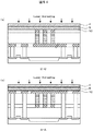
図1は本実施例の半導体記憶装置の平面図であり、実施例1〜4と同様である。図62〜65は図1におけるA−A線、B−B線、C−C線、D−D線、断面図である。また図66は、メモリアレイ部分だけを示した立体図である。なお、図1の平面図、図66の立体図において、図面を見やすくするために一部の部材は省略している。 FIG. 1 is a plan view of the semiconductor memory device of the present embodiment, which is the same as in the first to fourth embodiments. 62-65 are the AA line, BB line, CC line, DD line, and sectional drawing in FIG. FIG. 66 is a three-dimensional view showing only the memory array portion. In the plan view of FIG. 1 and the three-dimensional view of FIG. 66, some members are omitted to make the drawing easier to see.
本実施例の半導体記憶装置は、メモリ素子に抵抗可変素子である相変化メモリ、選択素子にポリシリコンダイオードを用いていて、これらが積層クロスポイント型にアレイを構成している点で実施例1〜4と同様であるが、ワード線やビット線を隣接メモリアレイ層で共用していない。そのため、選択素子となるダイオードの極性は隣接メモリ層で逆向きにする必要が無く、同じ向きで良い(図66)。 The semiconductor memory device of the present embodiment uses a phase change memory that is a resistance variable element as a memory element, and a polysilicon diode as a selection element. ˜4, but word lines and bit lines are not shared by adjacent memory array layers. Therefore, the polarity of the diode serving as the selection element does not need to be reversed in the adjacent memory layer, and may be the same direction (FIG. 66).
図62から66では4層積層の場合のメモリアレイを示しているが、5層以上を積層することももちろん可能である。
相変化素子の動作は図7で説明した通りである。また、読み出し時、セット/リセット時のメモリアレイ内のセル選択方式も図8、9で説明したのと同様である。
次に、図67〜図74を用いて上記積層相変化メモリの製造方法を説明する。
ST形成後に絶縁膜21でSTおよび、周辺回路のデバイスを埋め込み、必要に応じて化学的機械研磨法(CMP法)などで表面を平坦化したのが図67(a)の状態である。次にワード線となる例えばタングステン2、Bドープアモルファスシリコン14、不純物をドープしないアモルファスシリコン11を成膜する(図67(b))。タングステン膜2の成膜にはスパッタ法、Bドープアモルファスシリコン14、不純物をドープしないアモルファスシリコン11の成膜にはCVD法を用いた。タングステン成膜温度は200℃以下、Bドープアモルファスシリコンの成膜温度は400℃程度、不純物をドープしないアモルファスシリコン11の成膜温度は530℃程度である。次に、イオン打ち込み法によりリンイオンをアモルファスシリコン11にドープする(図67(c))。
62 to 66 show the memory array in the case of four-layer stacking, it is of course possible to stack five or more layers.
The operation of the phase change element is as described in FIG. Further, the cell selection method in the memory array at the time of reading and setting / resetting is the same as that described with reference to FIGS.
Next, the manufacturing method of the said laminated phase change memory is demonstrated using FIGS.
FIG. 67A shows a state in which ST and peripheral circuit devices are embedded in the insulating
次に例えばCO2レーザーアニールにより、アモルファスシリコン14、15を結晶化し不純物の活性化も行う(図68(a))。この時点では、相変化メモリ材料は含まれていないので、熱負荷低減の目的で行うレーザーアニールは必須ではなく、通常の加熱炉によるポリシリコンの結晶化、不純物の活性化を行うことも可能であるが、後述するように2層目以降のメモリアレイを製造する際には、レーザーアニールが必須である。本実施例では、1層目と2層目以降の選択素子の特性を同等にそろえるために、図68(a)の工程で2層目以降に用いるのと同じレーザーアニールを用いた。
Next, the
次に、WSi、TiSi2などのシリサイド10をPドープポリシリコン5の表面に形成し、相変化素子の下部電極となる8(TiN、Wなど)、相変化材料6(Ge2Sb2Te5など)、相変化素子の上部電極となる7(TiN、Wなど)を順に成膜した(図68(b))。
ポリシリコンによる積層PNダイオード構造は、図67、図68に示した方法以外の方法でも形成できる。
Next, a
The stacked PN diode structure made of polysilicon can also be formed by a method other than the method shown in FIGS.
実施例1に示した、別方法1(図12(a)(b))、別方法2(図12(c)(d))、別方法3(図13(a)〜(d))、別方法4(図14(a)〜(c))、別方法5(図15(a)〜(c))を用いることもできる。 Alternative method 1 (FIGS. 12A and 12B), alternative method 2 (FIGS. 12C and 12D), alternative method 3 (FIGS. 13A to 13D) shown in Example 1, Alternative method 4 (FIGS. 14A to 14C) and alternative method 5 (FIGS. 15A to 15C) can also be used.
図68(b)の次に、上部電極材料7、相変化材料6、下部電極材料8、シリサイド膜10、Pドープポリシリコン5、Bドープポリシリコン4、ワード線材料2をx方向に延在するストライプ状にパターニングした。この時、WL、GWLに至るコンタクト孔が形成される部分にはパターンを残す。メモリアレイ部分の立体図は図166となる。
次にシリコン酸化膜22を例えばCVD法で堆積し、図69でパターニングしたスペースが完全に埋まり込むようにする。次に、例えばCMP法で表面を平坦化し上部電極7を露出させる。次に、ビット線に接続する選択トランジスタの拡散層に至るコンタクト孔150を形成する。次に例えば孔150内に例えばCVD法でW、またはTi、TiN、Wを順に埋め込む。上表面に堆積したWを例えばCMP法で除去することでplugを形成した後、ビット線3となる材料(例えばタングステン)を成膜する。立体図は図70(b)となる。次にビット線材料、上部電極7、相変化材料6、下部電極8、シリサイド10、Pドープポリシリコン5、Bドープポリシリコン4をy方向に延在するストライプ状にパターニングした。またこの時、BL、GBLに至るコンタクト孔が形成される部分にはパターンを残す。1層目のメモリアレイのクロスポイント構造が完成する(図70(b))
次に、メモリアレイ層1層目と2層目を分離するための絶縁膜23を成膜した後、CMPで絶縁膜23の上表面を平坦化する。次に、ワード線1層目に至るコンタクト孔を形成し、次に例えばコンタクト孔内に例えばCVD法でW、またはTi、TiN、Wを順に埋め込む。上表面に堆積したWを例えばCMP法で除去することでplugを形成する。
68B, the
Next, a
Next, after forming an insulating
次にワード線となる例えばタングステン2、Bドープアモルファスシリコン14、不純物をドープしないアモルファスシリコン11を成膜する(図71(a))。タングステン膜2の成膜にはスパッタ法、Bドープアモルファスシリコン14、不純物をドープしないアモルファスシリコン11の成膜にはCVD法を用いた。タングステン成膜温度は200℃以下、Bドープアモルファスシリコンの成膜温度は400℃程度、不純物をドープしないアモルファスシリコン11の成膜温度は530℃程度である。
Next, for example,
次に、イオン打ち込み法によりリンイオンをアモルファスシリコン11にドープし(図71(b))、次に例えばCO2レーザーアニールにより、アモルファスシリコン14、15を結晶化し不純物の活性化も行う(図72(a))。
レーザーアニールは、アモルファスシリコンの結晶化と不純物の活性化を充分に行い、選択素子となるダイオードの電流駆動能力を充分なものにすること、1層目のメモリアレイを構成する相変化メモリ材料6への熱負荷を低減し歩留りを低下させないことを目的に行う。
Next, phosphorus ions are doped into the
The laser annealing sufficiently crystallizes the amorphous silicon and activates the impurities so that the current drive capability of the diode serving as the selection element is sufficient, and the phase
通常、炉体によるポリシリコンの結晶化には700℃以上の長時間熱処理が必要であり、この熱負荷で相変化素子の歩留りはほぼ0%にまで低下してしまう。相変化材料6と結晶化を行う2層目のアモルファスシリコンの間に、ビット線材料3が存在する状態で、レーザーアニールによる短時間アニールを行なうと、炉対加熱の場合と比較して、2層目のアモルファスシリコンを結晶化する際の相変化材料6の温度上昇を抑制でき熱負荷を低減できる。
Usually, a long time heat treatment of 700 ° C. or more is required for crystallization of polysilicon by a furnace body, and the yield of the phase change element is reduced to almost 0% by this heat load. When annealing is performed for a short time by laser annealing in the state where the
次に、WSi、TiSi2などのシリサイド10をPドープポリシリコン5の表面に形成し、相変化素子の下部電極となる8(TiN、Wなど)、相変化材料6(Ge2Sb2Te5など)、相変化素子の上部電極となる7(TiN、Wなど)を順に成膜した(図72(b))。立体図は、図73となる。
Next, a
以下1層目の形成と同様の工程を繰り返すことで、2層目、3層目、4層目のアレイを形成できた。
実施例1〜4の場合と同様に、炉体加熱により選択素子となるトランジスタのポリシリコン結晶化を行う従来の方法で製造すると、積層相変化メモリの選択素子の電流駆動能力と相変化素子の歩留りYmin以上を両立させることが不可能であった。本発明の方法で両立させることが可能となり、積層化による相変化メモリの低コスト大容量化が可能となった。
本実施例5では、抵抗可変素子を相変化メモリ、選択素子となるトランジスタをポリシリコンで形成したが、抵抗可変素子をNiO、CuO、TiO2などのReRAM、選択トランジスタをGe、SiGeなどのシリコン以外の半導体を用いることも可能であり、同様の効果を得ることができた。
Thereafter, the same process as the formation of the first layer was repeated to form an array of the second layer, the third layer, and the fourth layer.
As in the case of the first to fourth embodiments, when manufactured by the conventional method of performing polysilicon crystallization of the transistor serving as the selection element by furnace heating, the current driving capability of the selection element of the stacked phase change memory and the phase change element It was impossible to achieve both the yield Ymin and higher. The method of the present invention makes it possible to achieve both, and it is possible to increase the cost and capacity of the phase change memory by stacking.
In the fifth embodiment, the variable resistance element is formed of phase change memory and the transistor serving as the selection element is formed of polysilicon. However, the variable resistance element is formed of ReRAM such as NiO, CuO, and TiO 2, and the selection transistor is formed of silicon such as Ge and SiGe. Other semiconductors can be used, and the same effect can be obtained.
実施例1〜5では、メモリアレイの選択素子に用いるダイオードをポリシリコンのP-Nダイオード、あるいはP-I-Nダイオードで形成していたが、これらをポリシリコン/金属間のショットキーダイオードで形成することもできる。 In the first to fifth embodiments, the diode used for the selection element of the memory array is formed of a polysilicon PN diode or PIN diode. However, these may be formed of a polysilicon / metal Schottky diode. it can.
ショットキーダイオードはたとえば、図75〜図78に示す方法で形成できる。
ワード線、ビット線となる例えばタングステン上に、不純物をドープしないアモルファスシリコン11を成膜する(図75(a))。タングステン膜2の成膜にはスパッタ法、不純物をドープしないアモルファスシリコン11の成膜にはCVD法を用いた。タングステン成膜温度は200℃以下、不純物をドープしないアモルファスシリコン11の成膜温度は530℃程度である。次にイオン打ち込みによりBイオンをアモルファスシリコンにドープする。不純物イオンの濃度をアモルファスシリコンの下部電極側、特にタングステン表面側を高濃度にし、表面側は低濃度にする(図75(b))。次にレーザーアニールによりアモルファスシリコンを結晶化した後(図75(c))、電極8(たとえばTiN)を成膜する(図75(d))。このようにすることで、電流が上向き方向が順方向となるショットキーダイオードを形成することができる。
The Schottky diode can be formed, for example, by the method shown in FIGS.
ワード線、ビット線となる例えばタングステン上に、不純物をドープしないアモルファスシリコン11を成膜した後(図76(a))、イオン打ち込みによりBイオンをアモルファスシリコンにドープする際に、不純物イオンの濃度をアモルファスシリコンの上表面で高濃度にし下部電極側は低濃度にする(図76(b))。次にレーザーアニールによりアモルファスシリコンを結晶化した後(図76(c))、シリサイド膜9を成膜し、電極8(たとえばTiN)を成膜する(図76(d))。このようにすることで、電流が下向き方向が順方向となるショットキーダイオードを形成することができる。
After amorphous
ワード線、ビット線となる例えばタングステン上に、シリサイド膜10を成膜し、不純物をドープしないアモルファスシリコン11を成膜した後(図77(a))、イオン打ち込みによりPイオンをアモルファスシリコンにドープする。不純物イオンの濃度をアモルファスシリコンの下部電極側、特にタングステン表面側を高濃度にし、表面側は低濃度にする(図77(b))。次にレーザーアニールによりアモルファスシリコンを結晶化した後(図77(c))、電極8(たとえばTiN)を成膜する(図77(d))。このようにすることで、電流が下向き方向が順方向となるショットキーダイオードを形成することができる。
ワード線、ビット線の特に上表面をTiNにし、不純物をドープしないアモルファスシリコン11を成膜した後(図78(a))、イオン打ち込みによりPイオンをアモルファスシリコンにドープする。不純物イオンの濃度をアモルファスシリコンの上表面を高濃度にし、下部電極界面は低濃度にする(図78(b))。次にレーザーアニールによりアモルファスシリコンを結晶化した後(図78(c))、シリサイド膜10、電極8(たとえばTiN)を成膜する(図78(d))。このようにすることで、電流が上向き方向が順方向となるショットキーダイオードを形成することができる。
A
After the upper surfaces of the word lines and bit lines are particularly TiN and
図75〜78の製造方法のショットキーダイオードを用いた半導体記憶装置は、実施例1〜5の場合と同様に、炉体加熱により選択素子となるトランジスタのポリシリコン結晶化を行う従来の方法で製造すると、積層相変化メモリの選択素子の電流駆動能力と相変化素子の歩留りYmin以上を両立させることが不可能であった。本発明の方法で両立させることが可能となり、積層化による相変化メモリの低コスト大容量化が可能となった。
本実施例6では、抵抗可変素子を相変化メモリ、選択素子となるトランジスタをポリシリコンで形成したが、抵抗可変素子をNiO、CuO、TiO2などのReRAM、選択トランジスタをGe、SiGeなどのシリコン以外の半導体を用いることも可能であり、同様の効果を得ることができた。
The semiconductor memory device using the Schottky diode of the manufacturing method of FIGS. 75 to 78 is a conventional method for crystallizing polysilicon of a transistor serving as a selection element by furnace heating, as in the case of the first to fifth embodiments. When manufactured, it has been impossible to achieve both the current drive capability of the selection element of the stacked phase change memory and the yield Ymin or more of the phase change element. The method of the present invention makes it possible to achieve both, and it is possible to increase the cost and capacity of the phase change memory by stacking.
In the sixth embodiment, the resistance variable element is formed of phase change memory and the transistor as the selection element is formed of polysilicon, but the resistance variable element is ReRAM such as NiO, CuO, TiO 2, and the selection transistor is silicon such as Ge or SiGe. Other semiconductors can be used, and the same effect can be obtained.
実施例1〜6の半導体記憶装置製造方法で、相変化材料6の上部電極7、または上部電極7と下部電極8を、ワード線2、ビット線3よりも熱伝導率が小さい材料で形成することもできる。
実施例1〜6でレーザーアニールにより、ポリシリコンの結晶化を行う際に、相変化材料6の熱負荷を低減するためには、レーザーアニールにより結晶化されるポリシリコンの熱が、相変化材料6に伝わりにくくする方が良く、ワード線2、ビット線3、上部電極7、下部電極8を熱伝導率が低い金属で形成することが好ましい。
In the semiconductor memory device manufacturing method of
In order to reduce the thermal load of the
金属材料は、電気伝導率と熱伝導率の間に、ウィーデマン・フランツ則
熱伝導率 ÷ 電気伝導率 = ローレンツ数 × 絶対温度
が成り立つ。ここで、ローレンツ数は、2.45×10⁻⁸ WΩK―2である。つまり、熱伝導率が低い金属は、電気伝導率も低く、熱伝導率が高い金属は電気伝導率も低い。
ワード線2やビット線3は、相変化メモリの書換え、読出し時に電流を流すメモリアレイ内の長い配線を形成するため電気伝導率が十分高くしないと配線での電圧降下により相変化メモリの動作ができなくなるなどの不具合が生じる。それに対して、上部電極7や下部電極8は電流経路としては短く、配線ほど電気伝導率が高い必要が無い。
For metal materials, the Wiedemann-Franz law thermal conductivity ÷ electrical conductivity = Lorentz number × absolute temperature holds between electrical conductivity and thermal conductivity. Here, the Lorentz number is 2.45 × 10 −8 WΩK −2 . That is, a metal having a low thermal conductivity has a low electrical conductivity, and a metal having a high thermal conductivity has a low electrical conductivity.
Since the
そこで、上部電極7または上部電極7と下部電極8の両方をワード線2、ビット線3よりも熱伝導率が低い材料で形成することで、配線抵抗による相変化メモリの動作への悪影響を増加させることなく、レーザーアニールによるシリコンの結晶化の際の熱負荷を低減できる。実施例1〜6の製造方法で、例えば、TiNなどのような熱伝導率が小さい金属を上部電極7と下部電極8に用いて、W、Cuなどをワード線2、ビット線3に用いることで本実施例7の不揮発性半導体記憶装置を製造できた。
Therefore, by forming the
本発明の不揮発性半導体記憶装置は、携帯型パーソナルコンピュータやデジタルスチルカメラ等の小型携帯情報機器用記憶装置に用いて好適なものである。 The nonvolatile semiconductor memory device of the present invention is suitable for use in a memory device for small portable information devices such as a portable personal computer and a digital still camera.
1…半導体基板(シリコン基板)、
2…ワード線、
3…ビット線、
4…p型ポリシリコン、
5…n型ポリシリコン、
6…抵抗可変素子材料(例えば相変化材料)、
7…抵抗可変素子の上部電極、
8…抵抗可変素子の下部電極、
9…p型ポリシリコン界面のバリアメタル、またはシリサイド、
10…n型ポリシリコン界面のバリアメタル、またはシリサイド、
11…不純物をドープしていないアモルファスシリコン、
12…不純物をドープしていないポリシリコン、
14…p型不純物を高濃度に含むアモルファスシリコン、
15…n型不純物を高濃度に含むアモルファスシリコン、
44…p型不純物を低濃度に含むポリシリコン、
45…n型不純物を低濃度に含むポリシリコン、
54…p型不純物を低濃度に含むアモルファスシリコン、
55…n型不純物を低濃度に含むアモルファスシリコン、
20、21、22、23、24、25、26、27、28、29、31…シリコン酸化膜、
30…ハードマスク材料、
100…プレート電極、
120、121、122、123、124、125、126、127…絶縁膜、
150、151…コンタクト孔、
161…ゲート絶縁膜、
200…素子分離、
Gate…ゲート電極、
Dif…拡散層、
ST…選択トランジスタ、
plug…プラグ電極、
SWL…選択ワード線、
USWL…非選択ワード線、
SBL…選択ビット線、
USBL…非選択ビット線
SMC…選択メモリセル、
Sense Amp.…センスアンプ、
Icell…読み出し時選択セル電流、
Iread…読み出し時センスアンプ電流、
Iset…セット時選択セル電流、
Ireset…リセット時選択セル電流、
CellA…選択ワード線、選択ビット線メモリセル(選択メモリセル)、
CellB…非選択ワード線、選択ビット線メモリセル、
CellC…選択ワード線、非選択ビット線メモリセル、
CellD…非選択ワード線、非選択ビット線メモリセル、
u…選択ワード線の上層のビット線、
d…選択ワード線の下層のビット線。
1 ... Semiconductor substrate (silicon substrate),
2. Word line,
3 ... bit line,
4 ... p-type polysilicon,
5 ... n-type polysilicon,
6 ... variable resistance element material (for example, phase change material),
7: Upper electrode of variable resistance element,
8: Lower electrode of variable resistance element,
9: Barrier metal or silicide at the p-type polysilicon interface,
10: n-type polysilicon interface barrier metal or silicide,
11 ... amorphous silicon not doped with impurities,
12 ... polysilicon not doped with impurities,
14 ... amorphous silicon containing a high concentration of p-type impurities,
15: amorphous silicon containing n-type impurities at a high concentration,
44. Polysilicon containing a low concentration of p-type impurities,
45. Polysilicon containing n-type impurities at a low concentration,
54. Amorphous silicon containing a low concentration of p-type impurities,
55. Amorphous silicon containing n-type impurities at a low concentration,
20, 21, 22, 23, 24, 25, 26, 27, 28, 29, 31 ... silicon oxide film,
30 ... Hard mask material,
100: Plate electrode,
120, 121, 122, 123, 124, 125, 126, 127 ... insulating film,
150, 151 ... contact holes,
161: gate insulating film,
200: element isolation,
Gate ... gate electrode,
Dif ... diffusion layer,
ST: Selection transistor,
plug ... plug electrode,
SWL ... selected word line,
USWL: Unselected word line,
SBL ... selected bit line,
USBL ... unselected bit line SMC ... selected memory cell,
Sense Amp. ... sense amplifier,
Icell: Selected cell current at the time of reading,
Iread: Sense amplifier current when reading,
Iset: Selected cell current when set,
Ireset: selected cell current at reset,
CellA ... selected word line, selected bit line memory cell (selected memory cell),
CellB: Unselected word line, selected bit line memory cell,
CellC: selected word line, unselected bit line memory cell,
CellD: Unselected word line, unselected bit line memory cell,
u: Bit line above the selected word line,
d: Bit line below the selected word line.
Claims (20)
(1)半導体基板上に前記記録材料を堆積する工程と、
(2)前記記録材料が堆積された前記半導体基板の表面全体を覆うように金属膜を堆積する工程と、
(3)前記金属膜上に、前記半導体デバイスを構成するアモルファスシリコンを堆積する工程と、
(4)前記アモルファスシリコンを短時間アニールで結晶化する工程と、
を含むことを特徴とする半導体記憶装置の製造方法。 A method of manufacturing a semiconductor memory device having a structure in which semiconductor devices including a recording material such as a phase change material and a ReRAM material and a silicon material are stacked,
(1) depositing the recording material on a semiconductor substrate;
(2) depositing a metal film so as to cover the entire surface of the semiconductor substrate on which the recording material is deposited;
(3) depositing amorphous silicon constituting the semiconductor device on the metal film;
(4) crystallization of the amorphous silicon by short-time annealing;
A method for manufacturing a semiconductor memory device, comprising:
前記上部領域と前記下部領域のうちのいずれか他方の領域に、第2導電型の不純物領域を形成する工程を含むことを特徴とする請求項1に記載の半導体記憶装置の製造方法。 Before the step (4), an impurity region of the first conductivity type is formed in either the upper region located on the surface side of the amorphous silicon or the lower region located on the metal film side,
2. The method of manufacturing a semiconductor memory device according to claim 1, further comprising a step of forming a second conductivity type impurity region in one of the upper region and the lower region.
前記結晶化された第1導電型の不純物を含むシリコン上に第2のアモルファスシリコンを成膜した後、前記第2導電型の不純物領域をイオン打ち込みにより形成する工程とを有することを特徴とする請求項6に記載の半導体記憶装置の製造方法。 A step of crystallizing the amorphous silicon containing the first conductivity type impurity by short-time annealing after forming the amorphous silicon containing the first conductivity type impurity;
And forming a second conductive type impurity region by ion implantation after forming a second amorphous silicon film on the crystallized silicon containing the first conductive type impurity. A method for manufacturing a semiconductor memory device according to claim 6.
前記上部領域と前記下部領域のうちのいずれか他方の領域に、第1導電型の低濃度不純物領域を形成する工程を含むことを特徴とする請求項1に記載の半導体記憶装置の製造方法。 Prior to the step (4), a high-concentration impurity region of the first conductivity type is formed in either the upper region located on the surface side of the amorphous silicon or the lower region located on the metal film side. ,
2. The method of manufacturing a semiconductor memory device according to claim 1, further comprising a step of forming a first conductivity type low-concentration impurity region in one of the upper region and the lower region.
前記(2)の工程で前記半導体基板の表面全体を金属膜で覆う前に、前記ピラー状構造を加工する際の最小寸法を用いて前記記録材料をストライプ状またはドット状にパターニングすることを特徴とする請求項1に記載の半導体記憶装置の製造方法。 In forming a memory having a pillar structure in which the recording material and the semiconductor device are stacked,
Before the entire surface of the semiconductor substrate is covered with a metal film in the step (2), the recording material is patterned into a stripe shape or a dot shape using a minimum dimension for processing the pillar-like structure. A method of manufacturing a semiconductor memory device according to claim 1.
(A)半導体基板上に前記記録材料を成膜する工程と、
(B)前記記録材料が堆積された前記半導体基板の表面全体を覆うように絶縁膜を堆積する工程と、
(C)前記絶縁膜の表面全体を覆うように金属膜を堆積する工程と、
(D)前記金属膜上に前記ダイオードとなるアモルファスシリコンを堆積する工程と、
(E)アモルファスシリコンを短時間アニールで結晶化する工程と、
を含むことを特徴とする半導体記憶装置の製造方法。 A manufacturing method of a semiconductor memory device having a structure in which an array of memory cells including a recording material such as a phase change material or a ReRAM material and a silicon material to be a semiconductor device is laminated,
(A) forming a film of the recording material on a semiconductor substrate;
(B) depositing an insulating film so as to cover the entire surface of the semiconductor substrate on which the recording material is deposited;
(C) depositing a metal film so as to cover the entire surface of the insulating film;
(D) depositing amorphous silicon to be the diode on the metal film;
(E) a process of crystallizing amorphous silicon by short-time annealing;
A method for manufacturing a semiconductor memory device, comprising:
前記上部領域と前記下部領域のうちのいずれか他方の領域に、第2導電型の不純物領域を形成する工程を含むことを特徴とする請求項12に記載の半導体記憶装置の製造方法。 In the step (D), an impurity region of the first conductivity type is formed in either one of the upper region located on the surface side of the amorphous silicon or the lower region located on the metal film side,
13. The method of manufacturing a semiconductor memory device according to claim 12, further comprising a step of forming a second conductivity type impurity region in one of the upper region and the lower region.
前記上部領域と前記下部領域のうちのいずれか他方の領域に、第1導電型の低濃度不純物領域を形成する工程を含むことを特徴とする請求項12に記載の半導体記憶装置の製造方法。 In the step (D), a high-concentration impurity region of the first conductivity type is formed in either one of the upper region located on the surface side of the amorphous silicon or the lower region located on the metal film side,
13. The method of manufacturing a semiconductor memory device according to claim 12, further comprising a step of forming a first conductivity type low-concentration impurity region in either one of the upper region and the lower region.
前記(A)の記録材料を前記(B)の工程において、前記半導体基板の表面全体を絶縁膜で覆う前に、前記ピラー状構造を加工する際の最小寸法を用いて前記記録材料をストライプ状またはドット状にパターニングすることを特徴とする請求項12に記載の半導体記憶装置の製造方法。 In forming a memory having a pillar structure in which the recording material and the semiconductor device are stacked,
In the step (B), the recording material (A) is striped using the minimum dimension for processing the pillar-shaped structure before covering the entire surface of the semiconductor substrate with an insulating film. The method of manufacturing a semiconductor memory device according to claim 12, wherein patterning is performed in a dot shape.
前記絶縁膜上に形成された形成された複数の第1金属配線と、
前記第1金属配線上の各々に形成された複数のダイオードと、
前記ダイオードの各々の上に形成された第1電極と、
前記第1電極上に形成された相変化材料やReRAM材料などの記録材料と、
前記相変化材料の上に形成された第2電極と、
前記第2電極上に形成された複数の第2配線とを有し、
前記第1配線は、前記記録材料と前記第2配線とを介する前記第2電極よりも熱伝導率が大きい金属で形成されることを特徴とする半導体記憶装置。 An insulating film formed on the semiconductor substrate;
A plurality of first metal wirings formed on the insulating film;
A plurality of diodes formed on each of the first metal wirings;
A first electrode formed on each of the diodes;
A recording material such as a phase change material or a ReRAM material formed on the first electrode;
A second electrode formed on the phase change material;
A plurality of second wirings formed on the second electrode;
The semiconductor memory device, wherein the first wiring is formed of a metal having a higher thermal conductivity than the second electrode through the recording material and the second wiring.
Priority Applications (2)
| Application Number | Priority Date | Filing Date | Title |
|---|---|---|---|
| JP2008117055A JP2009267219A (en) | 2008-04-28 | 2008-04-28 | Semiconductor memory device and manufacturing method thereof |
| US12/430,539 US20090267047A1 (en) | 2008-04-28 | 2009-04-27 | Semiconductor memory device and manufacturing method thereof |
Applications Claiming Priority (1)
| Application Number | Priority Date | Filing Date | Title |
|---|---|---|---|
| JP2008117055A JP2009267219A (en) | 2008-04-28 | 2008-04-28 | Semiconductor memory device and manufacturing method thereof |
Publications (2)
| Publication Number | Publication Date |
|---|---|
| JP2009267219A true JP2009267219A (en) | 2009-11-12 |
| JP2009267219A5 JP2009267219A5 (en) | 2011-03-24 |
Family
ID=41214095
Family Applications (1)
| Application Number | Title | Priority Date | Filing Date |
|---|---|---|---|
| JP2008117055A Withdrawn JP2009267219A (en) | 2008-04-28 | 2008-04-28 | Semiconductor memory device and manufacturing method thereof |
Country Status (2)
| Country | Link |
|---|---|
| US (1) | US20090267047A1 (en) |
| JP (1) | JP2009267219A (en) |
Cited By (10)
| Publication number | Priority date | Publication date | Assignee | Title |
|---|---|---|---|---|
| JP2011119296A (en) * | 2009-11-30 | 2011-06-16 | Toshiba Corp | Resistance change memory and method of manufacturing the same |
| JP2011129737A (en) * | 2009-12-18 | 2011-06-30 | Toshiba Corp | Method of manufacturing semiconductor storage device, and semiconductor storage device |
| WO2011086725A1 (en) * | 2010-01-15 | 2011-07-21 | 株式会社日立製作所 | Nonvolatile storage device and manufacturing method therefor |
| JP2011165854A (en) * | 2010-02-09 | 2011-08-25 | Toshiba Corp | Memory device and method of manufacturing the same |
| JP2011198959A (en) * | 2010-03-18 | 2011-10-06 | Toshiba Corp | Method of manufacturing nonvolatile memory device |
| JP2011253943A (en) * | 2010-06-02 | 2011-12-15 | Hitachi Ltd | Semiconductor device and manufacturing method of the same |
| JP2013058582A (en) * | 2011-09-08 | 2013-03-28 | Toshiba Corp | Nonvolatile storage device manufacturing method |
| JP2014195111A (en) * | 2014-05-26 | 2014-10-09 | Toshiba Corp | Nonvolatile resistance change element |
| US11594677B2 (en) | 2019-09-17 | 2023-02-28 | Kioxia Corporation | Semiconductor storage device with insulating films adjacent resistance changing films |
| JP7433973B2 (en) | 2020-02-20 | 2024-02-20 | キオクシア株式会社 | Nonvolatile semiconductor memory device and its manufacturing method |
Families Citing this family (78)
| Publication number | Priority date | Publication date | Assignee | Title |
|---|---|---|---|---|
| US7768812B2 (en) | 2008-01-15 | 2010-08-03 | Micron Technology, Inc. | Memory cells, memory cell programming methods, memory cell reading methods, memory cell operating methods, and memory devices |
| US8034655B2 (en) | 2008-04-08 | 2011-10-11 | Micron Technology, Inc. | Non-volatile resistive oxide memory cells, non-volatile resistive oxide memory arrays, and methods of forming non-volatile resistive oxide memory cells and memory arrays |
| US8211743B2 (en) | 2008-05-02 | 2012-07-03 | Micron Technology, Inc. | Methods of forming non-volatile memory cells having multi-resistive state material between conductive electrodes |
| US8134137B2 (en) | 2008-06-18 | 2012-03-13 | Micron Technology, Inc. | Memory device constructions, memory cell forming methods, and semiconductor construction forming methods |
| US9343665B2 (en) | 2008-07-02 | 2016-05-17 | Micron Technology, Inc. | Methods of forming a non-volatile resistive oxide memory cell and methods of forming a non-volatile resistive oxide memory array |
| JP5329987B2 (en) * | 2009-01-09 | 2013-10-30 | 株式会社東芝 | Semiconductor memory device and manufacturing method thereof |
| US8144506B2 (en) | 2009-06-23 | 2012-03-27 | Micron Technology, Inc. | Cross-point memory devices, electronic systems including cross-point memory devices and methods of accessing a plurality of memory cells in a cross-point memory array |
| US8461566B2 (en) * | 2009-11-02 | 2013-06-11 | Micron Technology, Inc. | Methods, structures and devices for increasing memory density |
| US8411477B2 (en) | 2010-04-22 | 2013-04-02 | Micron Technology, Inc. | Arrays of vertically stacked tiers of non-volatile cross point memory cells, methods of forming arrays of vertically stacked tiers of non-volatile cross point memory cells, and methods of reading a data value stored by an array of vertically stacked tiers of non-volatile cross point memory cells |
| US8427859B2 (en) | 2010-04-22 | 2013-04-23 | Micron Technology, Inc. | Arrays of vertically stacked tiers of non-volatile cross point memory cells, methods of forming arrays of vertically stacked tiers of non-volatile cross point memory cells, and methods of reading a data value stored by an array of vertically stacked tiers of non-volatile cross point memory cells |
| US8289763B2 (en) | 2010-06-07 | 2012-10-16 | Micron Technology, Inc. | Memory arrays |
| US8946046B1 (en) | 2012-05-02 | 2015-02-03 | Crossbar, Inc. | Guided path for forming a conductive filament in RRAM |
| US9012307B2 (en) | 2010-07-13 | 2015-04-21 | Crossbar, Inc. | Two terminal resistive switching device structure and method of fabricating |
| US9601692B1 (en) | 2010-07-13 | 2017-03-21 | Crossbar, Inc. | Hetero-switching layer in a RRAM device and method |
| US9570678B1 (en) | 2010-06-08 | 2017-02-14 | Crossbar, Inc. | Resistive RAM with preferental filament formation region and methods |
| US8198144B2 (en) | 2010-06-11 | 2012-06-12 | Crossbar, Inc. | Pillar structure for memory device and method |
| US8374018B2 (en) | 2010-07-09 | 2013-02-12 | Crossbar, Inc. | Resistive memory using SiGe material |
| US8569172B1 (en) | 2012-08-14 | 2013-10-29 | Crossbar, Inc. | Noble metal/non-noble metal electrode for RRAM applications |
| US8884261B2 (en) | 2010-08-23 | 2014-11-11 | Crossbar, Inc. | Device switching using layered device structure |
| US8947908B2 (en) | 2010-11-04 | 2015-02-03 | Crossbar, Inc. | Hetero-switching layer in a RRAM device and method |
| US8168506B2 (en) | 2010-07-13 | 2012-05-01 | Crossbar, Inc. | On/off ratio for non-volatile memory device and method |
| US8492195B2 (en) | 2010-08-23 | 2013-07-23 | Crossbar, Inc. | Method for forming stackable non-volatile resistive switching memory devices |
| US8404553B2 (en) * | 2010-08-23 | 2013-03-26 | Crossbar, Inc. | Disturb-resistant non-volatile memory device and method |
| US9401475B1 (en) | 2010-08-23 | 2016-07-26 | Crossbar, Inc. | Method for silver deposition for a non-volatile memory device |
| US8889521B1 (en) | 2012-09-14 | 2014-11-18 | Crossbar, Inc. | Method for silver deposition for a non-volatile memory device |
| US8391049B2 (en) * | 2010-09-29 | 2013-03-05 | Crossbar, Inc. | Resistor structure for a non-volatile memory device and method |
| US8351242B2 (en) | 2010-09-29 | 2013-01-08 | Micron Technology, Inc. | Electronic devices, memory devices and memory arrays |
| US8558212B2 (en) | 2010-09-29 | 2013-10-15 | Crossbar, Inc. | Conductive path in switching material in a resistive random access memory device and control |
| US8759809B2 (en) | 2010-10-21 | 2014-06-24 | Micron Technology, Inc. | Integrated circuitry comprising nonvolatile memory cells having platelike electrode and ion conductive material layer |
| US8526213B2 (en) | 2010-11-01 | 2013-09-03 | Micron Technology, Inc. | Memory cells, methods of programming memory cells, and methods of forming memory cells |
| US8796661B2 (en) | 2010-11-01 | 2014-08-05 | Micron Technology, Inc. | Nonvolatile memory cells and methods of forming nonvolatile memory cell |
| US8502185B2 (en) | 2011-05-31 | 2013-08-06 | Crossbar, Inc. | Switching device having a non-linear element |
| USRE46335E1 (en) | 2010-11-04 | 2017-03-07 | Crossbar, Inc. | Switching device having a non-linear element |
| US9454997B2 (en) | 2010-12-02 | 2016-09-27 | Micron Technology, Inc. | Array of nonvolatile memory cells having at least five memory cells per unit cell, having a plurality of the unit cells which individually comprise three elevational regions of programmable material, and/or having a continuous volume having a combination of a plurality of vertically oriented memory cells and a plurality of horizontally oriented memory cells; array of vertically stacked tiers of nonvolatile memory cells |
| US8431458B2 (en) | 2010-12-27 | 2013-04-30 | Micron Technology, Inc. | Methods of forming a nonvolatile memory cell and methods of forming an array of nonvolatile memory cells |
| US8930174B2 (en) | 2010-12-28 | 2015-01-06 | Crossbar, Inc. | Modeling technique for resistive random access memory (RRAM) cells |
| US9153623B1 (en) | 2010-12-31 | 2015-10-06 | Crossbar, Inc. | Thin film transistor steering element for a non-volatile memory device |
| US8815696B1 (en) | 2010-12-31 | 2014-08-26 | Crossbar, Inc. | Disturb-resistant non-volatile memory device using via-fill and etchback technique |
| US8791010B1 (en) | 2010-12-31 | 2014-07-29 | Crossbar, Inc. | Silver interconnects for stacked non-volatile memory device and method |
| US8791447B2 (en) | 2011-01-20 | 2014-07-29 | Micron Technology, Inc. | Arrays of nonvolatile memory cells and methods of forming arrays of nonvolatile memory cells |
| US8488365B2 (en) | 2011-02-24 | 2013-07-16 | Micron Technology, Inc. | Memory cells |
| US8537592B2 (en) | 2011-04-15 | 2013-09-17 | Micron Technology, Inc. | Arrays of nonvolatile memory cells and methods of forming arrays of nonvolatile memory cells |
| JP2012248620A (en) * | 2011-05-26 | 2012-12-13 | Toshiba Corp | Manufacturing method of semiconductor memory device |
| US9620206B2 (en) | 2011-05-31 | 2017-04-11 | Crossbar, Inc. | Memory array architecture with two-terminal memory cells |
| US8619459B1 (en) | 2011-06-23 | 2013-12-31 | Crossbar, Inc. | High operating speed resistive random access memory |
| US9627443B2 (en) | 2011-06-30 | 2017-04-18 | Crossbar, Inc. | Three-dimensional oblique two-terminal memory with enhanced electric field |
| US9166163B2 (en) | 2011-06-30 | 2015-10-20 | Crossbar, Inc. | Sub-oxide interface layer for two-terminal memory |
| US9564587B1 (en) | 2011-06-30 | 2017-02-07 | Crossbar, Inc. | Three-dimensional two-terminal memory with enhanced electric field and segmented interconnects |
| US8946669B1 (en) | 2012-04-05 | 2015-02-03 | Crossbar, Inc. | Resistive memory device and fabrication methods |
| EP2735028A4 (en) | 2011-07-22 | 2015-05-06 | Crossbar Inc | Seed layer for a p + silicon germanium material for a non-volatile memory device and method |
| US9729155B2 (en) | 2011-07-29 | 2017-08-08 | Crossbar, Inc. | Field programmable gate array utilizing two-terminal non-volatile memory |
| US8674724B2 (en) | 2011-07-29 | 2014-03-18 | Crossbar, Inc. | Field programmable gate array utilizing two-terminal non-volatile memory |
| US10056907B1 (en) | 2011-07-29 | 2018-08-21 | Crossbar, Inc. | Field programmable gate array utilizing two-terminal non-volatile memory |
| JP5606479B2 (en) * | 2012-03-22 | 2014-10-15 | 株式会社東芝 | Semiconductor memory device |
| US9087576B1 (en) | 2012-03-29 | 2015-07-21 | Crossbar, Inc. | Low temperature fabrication method for a three-dimensional memory device and structure |
| US9685608B2 (en) | 2012-04-13 | 2017-06-20 | Crossbar, Inc. | Reduced diffusion in metal electrode for two-terminal memory |
| US8658476B1 (en) | 2012-04-20 | 2014-02-25 | Crossbar, Inc. | Low temperature P+ polycrystalline silicon material for non-volatile memory device |
| US8796658B1 (en) | 2012-05-07 | 2014-08-05 | Crossbar, Inc. | Filamentary based non-volatile resistive memory device and method |
| US8765566B2 (en) | 2012-05-10 | 2014-07-01 | Crossbar, Inc. | Line and space architecture for a non-volatile memory device |
| US10096653B2 (en) | 2012-08-14 | 2018-10-09 | Crossbar, Inc. | Monolithically integrated resistive memory using integrated-circuit foundry compatible processes |
| US9583701B1 (en) | 2012-08-14 | 2017-02-28 | Crossbar, Inc. | Methods for fabricating resistive memory device switching material using ion implantation |
| US8946673B1 (en) | 2012-08-24 | 2015-02-03 | Crossbar, Inc. | Resistive switching device structure with improved data retention for non-volatile memory device and method |
| US9312483B2 (en) | 2012-09-24 | 2016-04-12 | Crossbar, Inc. | Electrode structure for a non-volatile memory device and method |
| US9576616B2 (en) | 2012-10-10 | 2017-02-21 | Crossbar, Inc. | Non-volatile memory with overwrite capability and low write amplification |
| US11068620B2 (en) | 2012-11-09 | 2021-07-20 | Crossbar, Inc. | Secure circuit integrated with memory layer |
| US8982647B2 (en) | 2012-11-14 | 2015-03-17 | Crossbar, Inc. | Resistive random access memory equalization and sensing |
| US9412790B1 (en) | 2012-12-04 | 2016-08-09 | Crossbar, Inc. | Scalable RRAM device architecture for a non-volatile memory device and method |
| US9406379B2 (en) | 2013-01-03 | 2016-08-02 | Crossbar, Inc. | Resistive random access memory with non-linear current-voltage relationship |
| US9324942B1 (en) | 2013-01-31 | 2016-04-26 | Crossbar, Inc. | Resistive memory cell with solid state diode |
| US9112145B1 (en) | 2013-01-31 | 2015-08-18 | Crossbar, Inc. | Rectified switching of two-terminal memory via real time filament formation |
| US8934280B1 (en) | 2013-02-06 | 2015-01-13 | Crossbar, Inc. | Capacitive discharge programming for two-terminal memory cells |
| US10290801B2 (en) | 2014-02-07 | 2019-05-14 | Crossbar, Inc. | Scalable silicon based resistive memory device |
| KR102225782B1 (en) * | 2014-07-28 | 2021-03-10 | 삼성전자주식회사 | Variable resistance devices and methods of manufacturing the same |
| KR102463036B1 (en) | 2016-03-15 | 2022-11-03 | 삼성전자주식회사 | Semiconductor memory devices and methods of manufacturing the same |
| US11152569B2 (en) * | 2017-11-30 | 2021-10-19 | Taiwan Semiconductor Manufacturing Co., Ltd. | PCRAM structure with selector device |
| US10879313B2 (en) | 2019-05-13 | 2020-12-29 | Sandisk Technologies Llc | Three-dimensional cross-point memory device containing inter-level connection structures and method of making the same |
| US10991761B2 (en) * | 2019-05-13 | 2021-04-27 | Sandisk Technologies Llc | Three-dimensional cross-point memory device containing inter-level connection structures and method of making the same |
| KR20210077316A (en) | 2019-12-17 | 2021-06-25 | 삼성전자주식회사 | Variable resistance memory devices |
Family Cites Families (6)
| Publication number | Priority date | Publication date | Assignee | Title |
|---|---|---|---|---|
| DE19810793A1 (en) * | 1998-03-12 | 1999-09-16 | Basf Ag | Curable polyurethane polymer, dispersion based on this polymer, process for its preparation and its use |
| US6509217B1 (en) * | 1999-10-22 | 2003-01-21 | Damoder Reddy | Inexpensive, reliable, planar RFID tag structure and method for making same |
| JP3948292B2 (en) * | 2002-02-01 | 2007-07-25 | 株式会社日立製作所 | Semiconductor memory device and manufacturing method thereof |
| JP4529493B2 (en) * | 2004-03-12 | 2010-08-25 | 株式会社日立製作所 | Semiconductor device |
| US20070132049A1 (en) * | 2005-12-12 | 2007-06-14 | Stipe Barry C | Unipolar resistance random access memory (RRAM) device and vertically stacked architecture |
| US20080017890A1 (en) * | 2006-06-30 | 2008-01-24 | Sandisk 3D Llc | Highly dense monolithic three dimensional memory array and method for forming |
-
2008
- 2008-04-28 JP JP2008117055A patent/JP2009267219A/en not_active Withdrawn
-
2009
- 2009-04-27 US US12/430,539 patent/US20090267047A1/en not_active Abandoned
Cited By (14)
| Publication number | Priority date | Publication date | Assignee | Title |
|---|---|---|---|---|
| JP2011119296A (en) * | 2009-11-30 | 2011-06-16 | Toshiba Corp | Resistance change memory and method of manufacturing the same |
| US8975149B2 (en) | 2009-11-30 | 2015-03-10 | Kabushiki Kaisha Toshiba | Resistance change memory and manufacturing method thereof |
| JP2011129737A (en) * | 2009-12-18 | 2011-06-30 | Toshiba Corp | Method of manufacturing semiconductor storage device, and semiconductor storage device |
| WO2011086725A1 (en) * | 2010-01-15 | 2011-07-21 | 株式会社日立製作所 | Nonvolatile storage device and manufacturing method therefor |
| JP2011146590A (en) * | 2010-01-15 | 2011-07-28 | Hitachi Ltd | Nonvolatile memory device and method for manufacturing the same |
| JP2011165854A (en) * | 2010-02-09 | 2011-08-25 | Toshiba Corp | Memory device and method of manufacturing the same |
| US8546196B2 (en) | 2010-03-18 | 2013-10-01 | Kabushiki Kaisha Toshiba | Non-volatile memory device and manufacturing method thereof |
| JP2011198959A (en) * | 2010-03-18 | 2011-10-06 | Toshiba Corp | Method of manufacturing nonvolatile memory device |
| JP2011253943A (en) * | 2010-06-02 | 2011-12-15 | Hitachi Ltd | Semiconductor device and manufacturing method of the same |
| JP2013058582A (en) * | 2011-09-08 | 2013-03-28 | Toshiba Corp | Nonvolatile storage device manufacturing method |
| US9048176B2 (en) | 2011-09-08 | 2015-06-02 | Kabushiki Kaisha Toshiba | Nonvolatile storage device |
| JP2014195111A (en) * | 2014-05-26 | 2014-10-09 | Toshiba Corp | Nonvolatile resistance change element |
| US11594677B2 (en) | 2019-09-17 | 2023-02-28 | Kioxia Corporation | Semiconductor storage device with insulating films adjacent resistance changing films |
| JP7433973B2 (en) | 2020-02-20 | 2024-02-20 | キオクシア株式会社 | Nonvolatile semiconductor memory device and its manufacturing method |
Also Published As
| Publication number | Publication date |
|---|---|
| US20090267047A1 (en) | 2009-10-29 |
Similar Documents
| Publication | Publication Date | Title |
|---|---|---|
| JP2009267219A (en) | Semiconductor memory device and manufacturing method thereof | |
| US9450023B1 (en) | Vertical bit line non-volatile memory with recessed word lines | |
| JP3948292B2 (en) | Semiconductor memory device and manufacturing method thereof | |
| JP5481564B2 (en) | Nonvolatile memory device and manufacturing method thereof | |
| JP5512700B2 (en) | Semiconductor memory device and manufacturing method thereof | |
| JP4577693B2 (en) | Nonvolatile memory device and manufacturing method thereof | |
| JP5160116B2 (en) | Nonvolatile memory device | |
| CN108122923B (en) | Memory device and method of manufacturing the same | |
| US9893281B2 (en) | Semiconductor device and method of fabricating the same | |
| JP2008277543A (en) | Nonvolatile semiconductor memory device | |
| JP5420436B2 (en) | Nonvolatile memory device and manufacturing method thereof | |
| JP2011199035A (en) | Semiconductor memory device | |
| JP2009252974A (en) | Nonvolatile semiconductor memory device and method of manufacturing the same | |
| JP2011233831A (en) | Semiconductor memory device | |
| TWI550621B (en) | Circuit and system of using junction diode as program selector for electrical fuses with extended area for one-time programmable devices | |
| JP5634002B2 (en) | Phase change nonvolatile memory and semiconductor device | |
| JP2009206418A (en) | Nonvolatile memory device and manufacturing method for the same | |
| JP2007019559A (en) | Semiconductor storage device and its manufacturing method | |
| JP5279879B2 (en) | Nonvolatile semiconductor memory device | |
| US9209225B2 (en) | Cell structure of resistive non-volatile memory and manufacturing method thereof | |
| JP5386528B2 (en) | Semiconductor memory device and manufacturing method thereof | |
| US20160099290A1 (en) | Memory device | |
| TWI704705B (en) | Semiconductor memory device | |
| JP2010161137A (en) | Method of manufacturing semiconductor memory device | |
| JP2015153974A (en) | semiconductor memory device |
Legal Events
| Date | Code | Title | Description |
|---|---|---|---|
| A521 | Request for written amendment filed |
Free format text: JAPANESE INTERMEDIATE CODE: A523 Effective date: 20110207 |
|
| A621 | Written request for application examination |
Free format text: JAPANESE INTERMEDIATE CODE: A621 Effective date: 20110207 |
|
| A761 | Written withdrawal of application |
Free format text: JAPANESE INTERMEDIATE CODE: A761 Effective date: 20110215 |