JP2009246085A - Semiconductor device, and method of manufacturing the same - Google Patents
Semiconductor device, and method of manufacturing the same Download PDFInfo
- Publication number
- JP2009246085A JP2009246085A JP2008089776A JP2008089776A JP2009246085A JP 2009246085 A JP2009246085 A JP 2009246085A JP 2008089776 A JP2008089776 A JP 2008089776A JP 2008089776 A JP2008089776 A JP 2008089776A JP 2009246085 A JP2009246085 A JP 2009246085A
- Authority
- JP
- Japan
- Prior art keywords
- layer
- semiconductor device
- group
- memory
- memory layer
- Prior art date
- Legal status (The legal status is an assumption and is not a legal conclusion. Google has not performed a legal analysis and makes no representation as to the accuracy of the status listed.)
- Withdrawn
Links
- 239000004065 semiconductor Substances 0.000 title claims abstract description 49
- 238000004519 manufacturing process Methods 0.000 title claims description 26
- 239000013078 crystal Substances 0.000 claims abstract description 32
- 239000000203 mixture Substances 0.000 claims abstract description 29
- 229910052760 oxygen Inorganic materials 0.000 claims abstract description 16
- 230000008859 change Effects 0.000 claims abstract description 8
- 239000010410 layer Substances 0.000 claims description 111
- 239000000463 material Substances 0.000 claims description 48
- 238000000034 method Methods 0.000 claims description 24
- 229910052751 metal Inorganic materials 0.000 claims description 18
- 239000002184 metal Substances 0.000 claims description 18
- 229910052802 copper Inorganic materials 0.000 claims description 16
- 239000000758 substrate Substances 0.000 claims description 16
- 229910052715 tantalum Inorganic materials 0.000 claims description 12
- 238000010438 heat treatment Methods 0.000 claims description 11
- 239000011229 interlayer Substances 0.000 claims description 11
- 238000003860 storage Methods 0.000 claims description 11
- 230000015572 biosynthetic process Effects 0.000 claims description 9
- 229910052737 gold Inorganic materials 0.000 claims description 9
- 229910052709 silver Inorganic materials 0.000 claims description 9
- 229910052725 zinc Inorganic materials 0.000 claims description 9
- 229910052717 sulfur Inorganic materials 0.000 claims description 8
- QVGXLLKOCUKJST-UHFFFAOYSA-N atomic oxygen Chemical compound [O] QVGXLLKOCUKJST-UHFFFAOYSA-N 0.000 claims description 6
- 239000001301 oxygen Substances 0.000 claims description 6
- 229910052721 tungsten Inorganic materials 0.000 claims description 5
- ATJFFYVFTNAWJD-UHFFFAOYSA-N Tin Chemical compound [Sn] ATJFFYVFTNAWJD-UHFFFAOYSA-N 0.000 claims description 4
- 229910052710 silicon Inorganic materials 0.000 claims description 4
- 239000010703 silicon Substances 0.000 claims description 4
- 229910052718 tin Inorganic materials 0.000 claims description 4
- 229910010037 TiAlN Inorganic materials 0.000 claims description 2
- -1 TiSiC Inorganic materials 0.000 claims description 2
- 150000001721 carbon Chemical class 0.000 claims description 2
- 229910052750 molybdenum Inorganic materials 0.000 claims description 2
- 238000000137 annealing Methods 0.000 claims 7
- 229910052711 selenium Inorganic materials 0.000 claims 4
- 229910052714 tellurium Inorganic materials 0.000 claims 4
- 229910052688 Gadolinium Inorganic materials 0.000 claims 1
- 229910008599 TiW Inorganic materials 0.000 claims 1
- 239000011817 metal compound particle Substances 0.000 claims 1
- 239000002923 metal particle Substances 0.000 claims 1
- 229910052719 titanium Inorganic materials 0.000 claims 1
- 150000002500 ions Chemical class 0.000 abstract description 88
- 239000007784 solid electrolyte Substances 0.000 abstract description 26
- 239000010949 copper Substances 0.000 description 47
- 238000002425 crystallisation Methods 0.000 description 17
- 230000008025 crystallization Effects 0.000 description 14
- 238000009792 diffusion process Methods 0.000 description 12
- 150000001768 cations Chemical class 0.000 description 10
- 238000010586 diagram Methods 0.000 description 10
- 238000005229 chemical vapour deposition Methods 0.000 description 8
- 230000008569 process Effects 0.000 description 8
- 150000001450 anions Chemical class 0.000 description 7
- 238000004544 sputter deposition Methods 0.000 description 6
- 229910052581 Si3N4 Inorganic materials 0.000 description 4
- 230000002093 peripheral effect Effects 0.000 description 4
- HQVNEWCFYHHQES-UHFFFAOYSA-N silicon nitride Chemical compound N12[Si]34N5[Si]62N3[Si]51N64 HQVNEWCFYHHQES-UHFFFAOYSA-N 0.000 description 4
- XUIMIQQOPSSXEZ-UHFFFAOYSA-N Silicon Chemical compound [Si] XUIMIQQOPSSXEZ-UHFFFAOYSA-N 0.000 description 3
- 230000004888 barrier function Effects 0.000 description 3
- 101150089047 cutA gene Proteins 0.000 description 3
- 230000006866 deterioration Effects 0.000 description 3
- 238000001312 dry etching Methods 0.000 description 3
- 230000000694 effects Effects 0.000 description 3
- 230000005684 electric field Effects 0.000 description 3
- 239000000126 substance Substances 0.000 description 3
- VYPSYNLAJGMNEJ-UHFFFAOYSA-N Silicium dioxide Chemical compound O=[Si]=O VYPSYNLAJGMNEJ-UHFFFAOYSA-N 0.000 description 2
- 230000007423 decrease Effects 0.000 description 2
- 239000002019 doping agent Substances 0.000 description 2
- 238000002474 experimental method Methods 0.000 description 2
- 230000006870 function Effects 0.000 description 2
- 238000005259 measurement Methods 0.000 description 2
- 238000005498 polishing Methods 0.000 description 2
- 229910052814 silicon oxide Inorganic materials 0.000 description 2
- 239000007787 solid Substances 0.000 description 2
- 229910002531 CuTe Inorganic materials 0.000 description 1
- BOTDANWDWHJENH-UHFFFAOYSA-N Tetraethyl orthosilicate Chemical compound CCO[Si](OCC)(OCC)OCC BOTDANWDWHJENH-UHFFFAOYSA-N 0.000 description 1
- 239000000956 alloy Substances 0.000 description 1
- 229910045601 alloy Inorganic materials 0.000 description 1
- 238000004380 ashing Methods 0.000 description 1
- 230000005540 biological transmission Effects 0.000 description 1
- 229910021387 carbon allotrope Inorganic materials 0.000 description 1
- 239000004020 conductor Substances 0.000 description 1
- 238000002050 diffraction method Methods 0.000 description 1
- 239000003792 electrolyte Substances 0.000 description 1
- 238000010894 electron beam technology Methods 0.000 description 1
- 238000002003 electron diffraction Methods 0.000 description 1
- 238000002524 electron diffraction data Methods 0.000 description 1
- 238000005516 engineering process Methods 0.000 description 1
- 238000005530 etching Methods 0.000 description 1
- 229940075613 gadolinium oxide Drugs 0.000 description 1
- 229910001938 gadolinium oxide Inorganic materials 0.000 description 1
- CMIHHWBVHJVIGI-UHFFFAOYSA-N gadolinium(iii) oxide Chemical compound [O-2].[O-2].[O-2].[Gd+3].[Gd+3] CMIHHWBVHJVIGI-UHFFFAOYSA-N 0.000 description 1
- 239000012212 insulator Substances 0.000 description 1
- 238000010030 laminating Methods 0.000 description 1
- 230000008018 melting Effects 0.000 description 1
- 238000002844 melting Methods 0.000 description 1
- 229910021645 metal ion Inorganic materials 0.000 description 1
- 239000007769 metal material Substances 0.000 description 1
- 239000012299 nitrogen atmosphere Substances 0.000 description 1
- 230000006911 nucleation Effects 0.000 description 1
- 238000010899 nucleation Methods 0.000 description 1
- 239000002245 particle Substances 0.000 description 1
- 238000001556 precipitation Methods 0.000 description 1
- 238000003672 processing method Methods 0.000 description 1
- 229910052761 rare earth metal Inorganic materials 0.000 description 1
- 238000006722 reduction reaction Methods 0.000 description 1
- 238000001878 scanning electron micrograph Methods 0.000 description 1
- QZCHKAUWIRYEGK-UHFFFAOYSA-N tellanylidenecopper Chemical compound [Te]=[Cu] QZCHKAUWIRYEGK-UHFFFAOYSA-N 0.000 description 1
- 239000011800 void material Substances 0.000 description 1
Images


Classifications
-
- H—ELECTRICITY
- H10—SEMICONDUCTOR DEVICES; ELECTRIC SOLID-STATE DEVICES NOT OTHERWISE PROVIDED FOR
- H10B—ELECTRONIC MEMORY DEVICES
- H10B63/00—Resistance change memory devices, e.g. resistive RAM [ReRAM] devices
- H10B63/30—Resistance change memory devices, e.g. resistive RAM [ReRAM] devices comprising selection components having three or more electrodes, e.g. transistors
-
- H—ELECTRICITY
- H10—SEMICONDUCTOR DEVICES; ELECTRIC SOLID-STATE DEVICES NOT OTHERWISE PROVIDED FOR
- H10B—ELECTRONIC MEMORY DEVICES
- H10B63/00—Resistance change memory devices, e.g. resistive RAM [ReRAM] devices
- H10B63/80—Arrangements comprising multiple bistable or multi-stable switching components of the same type on a plane parallel to the substrate, e.g. cross-point arrays
-
- H—ELECTRICITY
- H10—SEMICONDUCTOR DEVICES; ELECTRIC SOLID-STATE DEVICES NOT OTHERWISE PROVIDED FOR
- H10N—ELECTRIC SOLID-STATE DEVICES NOT OTHERWISE PROVIDED FOR
- H10N70/00—Solid-state devices having no potential barriers, and specially adapted for rectifying, amplifying, oscillating or switching
- H10N70/011—Manufacture or treatment of multistable switching devices
- H10N70/021—Formation of switching materials, e.g. deposition of layers
- H10N70/026—Formation of switching materials, e.g. deposition of layers by physical vapor deposition, e.g. sputtering
-
- H—ELECTRICITY
- H10—SEMICONDUCTOR DEVICES; ELECTRIC SOLID-STATE DEVICES NOT OTHERWISE PROVIDED FOR
- H10N—ELECTRIC SOLID-STATE DEVICES NOT OTHERWISE PROVIDED FOR
- H10N70/00—Solid-state devices having no potential barriers, and specially adapted for rectifying, amplifying, oscillating or switching
- H10N70/011—Manufacture or treatment of multistable switching devices
- H10N70/041—Modification of switching materials after formation, e.g. doping
-
- H—ELECTRICITY
- H10—SEMICONDUCTOR DEVICES; ELECTRIC SOLID-STATE DEVICES NOT OTHERWISE PROVIDED FOR
- H10N—ELECTRIC SOLID-STATE DEVICES NOT OTHERWISE PROVIDED FOR
- H10N70/00—Solid-state devices having no potential barriers, and specially adapted for rectifying, amplifying, oscillating or switching
- H10N70/20—Multistable switching devices, e.g. memristors
- H10N70/24—Multistable switching devices, e.g. memristors based on migration or redistribution of ionic species, e.g. anions, vacancies
- H10N70/245—Multistable switching devices, e.g. memristors based on migration or redistribution of ionic species, e.g. anions, vacancies the species being metal cations, e.g. programmable metallization cells
-
- H—ELECTRICITY
- H10—SEMICONDUCTOR DEVICES; ELECTRIC SOLID-STATE DEVICES NOT OTHERWISE PROVIDED FOR
- H10N—ELECTRIC SOLID-STATE DEVICES NOT OTHERWISE PROVIDED FOR
- H10N70/00—Solid-state devices having no potential barriers, and specially adapted for rectifying, amplifying, oscillating or switching
- H10N70/801—Constructional details of multistable switching devices
- H10N70/821—Device geometry
- H10N70/826—Device geometry adapted for essentially vertical current flow, e.g. sandwich or pillar type devices
-
- H—ELECTRICITY
- H10—SEMICONDUCTOR DEVICES; ELECTRIC SOLID-STATE DEVICES NOT OTHERWISE PROVIDED FOR
- H10N—ELECTRIC SOLID-STATE DEVICES NOT OTHERWISE PROVIDED FOR
- H10N70/00—Solid-state devices having no potential barriers, and specially adapted for rectifying, amplifying, oscillating or switching
- H10N70/801—Constructional details of multistable switching devices
- H10N70/841—Electrodes
- H10N70/8416—Electrodes adapted for supplying ionic species
-
- H—ELECTRICITY
- H10—SEMICONDUCTOR DEVICES; ELECTRIC SOLID-STATE DEVICES NOT OTHERWISE PROVIDED FOR
- H10N—ELECTRIC SOLID-STATE DEVICES NOT OTHERWISE PROVIDED FOR
- H10N70/00—Solid-state devices having no potential barriers, and specially adapted for rectifying, amplifying, oscillating or switching
- H10N70/801—Constructional details of multistable switching devices
- H10N70/881—Switching materials
- H10N70/883—Oxides or nitrides
- H10N70/8836—Complex metal oxides, e.g. perovskites, spinels
Landscapes
- Engineering & Computer Science (AREA)
- Manufacturing & Machinery (AREA)
- Chemical & Material Sciences (AREA)
- Materials Engineering (AREA)
- Semiconductor Memories (AREA)
Abstract
Description
本発明は、半導体装置およびその製造方法に係り、特に、抵抗の差を利用して記憶情報を弁別する固体電解質材料を用いたメモリセル、例えば、高密度集積メモリ回路、あるいはメモリ回路と論理回路とが同一半導体基板に設けられたロジック混載型メモリ、あるいはアナログ回路を有する半導体集積回路装置に適用して有効な技術に関するものであり、さらに、低電圧で動作する、高速かつ、不揮発性を有するランダムアクセスメモリに関する。 The present invention relates to a semiconductor device and a method for manufacturing the same, and more particularly to a memory cell using a solid electrolyte material that discriminates stored information using a difference in resistance, for example, a high density integrated memory circuit, or a memory circuit and a logic circuit. Relates to a technology that is effective when applied to a logic-embedded memory provided on the same semiconductor substrate or a semiconductor integrated circuit device having an analog circuit, and operates at a low voltage and has high speed and non-volatility It relates to random access memory.
固体電解質材料を用いた記録技術として、固体電解質メモリが提案されている。非特許文献1及び2には固体電解質メモリの詳細が記述されている。このメモリの記憶部とその周辺の構造を図2を用いて説明する。固体電解質メモリは記憶部RMをBECと上部電極15で挟んだ構造を持つ。記憶部RMは、固体電解質層21とイオン供給源となる電極22の積層構造を持つ。固体電荷質21中でモビリティの高いイオンが移動する。「モビリティが高いイオン」は、ある電解質中において、一定の電圧を印加したときに長距離移動するイオンと定義する。電極22の材料はモビリティの高い元素A(例えば、Cu)である。
A solid electrolyte memory has been proposed as a recording technique using a solid electrolyte material. Non-Patent
固体電解質21の材料は例えば、組成がCuとSである合金であり、固体電解質21はイオンAを含む。BECはイオン伝導度の低いプラグ材料13と密着層14の積層で形成される。上部電極15はモビリティの低い金属材料を用いる。それにより電界を印加したときに移動することを防止する。記憶部RMの抵抗が低い’ON状態’では固体電解質中に金属Aにより形成させた電気伝導性フィラメントが電極22−BEC間を接続している。
The material of the
一方、記憶部RMの抵抗が高い’OFF状態’では、電気伝導性フィラメントが切断されている。動作方法を以下に述べる。値の読み出しは。記憶部RMの抵抗を測定し、その高低をそれぞれ’0’と’1’に対応させる。記憶部RMを’ON状態’にする’ON動作’は以下のように行う。電極22に正の電圧を印加することで、電極22を酸化し、イオンAにする。その後、イオンAは固体電解質中をイオン伝導し、下部電極BECもしくはフィラメント近傍で還元されることで、フィラメントが生成もしくは成長する。フィラメントが電極22−BEC間を結ぶことで、記憶部RMは低抵抗になる。記憶部RMを’OFF状態’にする’OFF動作’は以下のように行う。電極Aに負の電圧を印加することで、フィラメントを構成する金属Aを酸化し、イオンAにする。その後、イオンAは固体電解質中に拡散する。
On the other hand, in the “OFF state” where the resistance of the memory unit RM is high, the electrically conductive filament is cut. The operation method is described below. Read the value. The resistance of the storage unit RM is measured, and the heights thereof correspond to “0” and “1”, respectively. The “ON operation” for setting the storage unit RM to the “ON state” is performed as follows. By applying a positive voltage to the
また、CuおよびTa、Oからなり、組成比がCu−Ta−O=1:2:6に近い結晶構造が非特許文献3で報告されている。以下、上記結晶をCu−Ta−O結晶とする。
Further,
特許文献1では酸化物材料を用いた半導体メモリが記載されている。金属フィラメントを形成もしくは消滅させることにより抵抗変化を生じさせている。特許文献1の半導体メモリは金属フィラメントの生成・消滅場所が酸化物材料内ではない。
また、特許文献2では2つの電極間に例えばCuTe(銅テルル化合物とGdOx(ガドリニウム酸化物)の積層を挟んだ構造の半導体メモリが記載されており、GdOx材料内に金属元素(例えばCu)を添加することにより記憶層の耐圧の向上させる方法が述べられている。
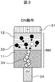
固体電解質メモリには書き換えを繰り返すことで固体電解質中のイオンA量及び電極の形状が変化してしまうため、安定した書き換えが困難である課題がある。これを解決するために我々が検討している回路装置の代表的な構造を図3を用いて説明する。イオンAの供給層は従来の固体電解質メモリでは電極Aであったが、本メモリでは固体電解質材料とした。例えばCu−Ta−Sである。以下、Cu−Ta−Sを例にして説明する。また、フィラメント形成部を三元系の酸化物とした。例えばCu−Ta−Oである。以下、Cu−Ta−Oを例にして説明する。さらに、以下、フィラメント形成部をイオン閉じ込め層とする。この構造にすることで得られる効果を以下に述べる。第1点は、イオン供給源を電極Aから固体電解質Cu−Ta−Sに変更することで供給可能なイオン総量を制限し、さらにイオン供給源の空隙の生成などの物理的変化を抑える。第2点は、モビリティの異なるCuとTaを金属イオンとして用いることである。モビリティの低いTaは、TaSやTaOの安定構造を作る。一方、モビリティの高いCuは、電気伝導性フィラメントを生成・消滅させることで、記憶部RMの抵抗変化を生じさせる。 The solid electrolyte memory has a problem that stable rewriting is difficult because the amount of ions A in the solid electrolyte and the shape of the electrode change due to repeated rewriting. In order to solve this problem, a typical structure of the circuit device we are examining will be described with reference to FIG. The supply layer of ions A is the electrode A in the conventional solid electrolyte memory, but is a solid electrolyte material in this memory. For example, Cu-Ta-S. Hereinafter, description will be given by taking Cu-Ta-S as an example. Further, the filament forming part was made of a ternary oxide. For example, Cu—Ta—O. Hereinafter, description will be made by taking Cu-Ta-O as an example. Further, hereinafter, the filament forming portion is referred to as an ion confinement layer. The effects obtained by this structure will be described below. The first point is to limit the total amount of ions that can be supplied by changing the ion supply source from the electrode A to the solid electrolyte Cu—Ta—S, and further suppress physical changes such as the generation of voids in the ion supply source. The second point is to use Cu and Ta having different mobility as metal ions. Ta with low mobility creates a stable structure of TaS and TaO. On the other hand, Cu with high mobility causes a resistance change of the memory unit RM by generating and annihilating the electrically conductive filament.
まず、図3を用いてON動作について述べる。上部電極31に下部電極34よりも高い電圧を印加することで、固体電荷質であるCu供給層中の正の電荷を持つCuイオン33はイオン伝導し、イオン閉じ込め層11へと移動する。説明を簡単にするために、以下の説明では上部電極には正の電圧が印加され、下部電極は0Vに保たれているとする。イオン閉じ込め層11において、Cuイオン33は還元反応により、金属Cu34になる。金属Cu34はイオン閉じ込め層11の電流が特に流れる部分に生成する。また、金属Cu34が生成するとその部分の抵抗が下がり、電流が集中する。そのため、金属Cu34はフィラメント形状を持つことが多い。Cuフィラメントが形成されることにより、記憶部RMの抵抗は低下する。
First, the ON operation will be described with reference to FIG. By applying a voltage higher than that of the
次に、図4を用いてOFF動作について説明する。上部電極32に負の電圧を印加し、下部電極34を0Vに保つことで、Cuフィラメント中の金属Cu34は酸化され、Cuイオンになる。その結果、Cuフィラメントの一部は消滅し、記憶部RMは高抵抗化する。Cuイオンは、イオン伝導により、Cu供給層12中に移動する。
Next, the OFF operation will be described with reference to FIG. By applying a negative voltage to the
上記の説明を図5に示す電流−電圧波形を用いて再度説明する。この波形は半導体パラメータアナライザを用いて測定した。上部電極電圧を約0.3V印加することで、ON動作51が生じ、抵抗が減少する。電圧を約0.5V印加した時点で、電流が300マイクロアンペアという一定の値を示しているが、これは測定機器のコンプライアンス電流に到達したためである。次に、上部電極電圧に約−0.3Vの電圧を印加することで、OFF動作52が生じ、抵抗が上昇する。上記の各説明は、動作時の電圧の極性を逆にしても成り立つ。また、イオン閉じ込め層とイオン供給層の上下関係を逆にしても成り立つ。
以上のように我々は高信頼動作を目指して本回路装置を検討している。
但し、高信頼用途向けDRAM(ダイナミックアクセスメモリ)などの一部用途においては、さらに信頼性の高い動作が要求される。
The above description will be described again using the current-voltage waveform shown in FIG. This waveform was measured using a semiconductor parameter analyzer. By applying the upper electrode voltage of about 0.3 V, the
As described above, we are studying this circuit device aiming at highly reliable operation.
However, in some applications such as DRAM (dynamic access memory) for high reliability applications, operation with higher reliability is required.
本発明が解決しようとする技術的課題は、前記技術の問題点を改善するためのものであって、信頼性の高いメモリ素子などの回路装置を提供することである。具体的には、エンデュランス回数の増加と書き換え電圧や書き換え抵抗のばらつきを低減させる。 A technical problem to be solved by the present invention is to provide a circuit device such as a highly reliable memory element, in order to improve the problems of the above technique. Specifically, the increase in the number of endurances and variations in the rewrite voltage and rewrite resistance are reduced.
前記課題を達成するために、本発明は、記憶部RMのイオン閉じ込め層の相状態が結晶である半導体装置を提供する。特に、結晶状態であるイオン閉じ込め層は、モビリティの高いイオンAとイオンAに比べてモビリティの低いイオンC、さらにイオンAおよびイオンCと逆の極性を持つイオンDの組成を持つ。結晶状態であるイオン閉じ込め層の組成の例は、Cu−Ta−O=1:2:6である。結晶化したイオン閉じ込め層は安定であるため、書き換え動作を行った場合の記憶部RMの物理的変形や記憶部内の組成比の過剰な変動が生じにくい。そのため、安定な書き換え動作が可能である。 In order to achieve the above object, the present invention provides a semiconductor device in which a phase state of an ion confinement layer of a memory unit RM is a crystal. In particular, the ion confinement layer in a crystalline state has a composition of ions A having a high mobility compared to ions A and A having a high mobility, and ions D having a polarity opposite to that of the ions A and C. An example of the composition of the ion confinement layer in the crystalline state is Cu—Ta—O = 1: 2: 6. Since the crystallized ion confinement layer is stable, physical deformation of the storage unit RM and excessive variation of the composition ratio in the storage unit are unlikely to occur when a rewrite operation is performed. Therefore, a stable rewrite operation is possible.
本願において開示される発明のうち、代表的なものによって得られる効果を簡単に述べると以下のとおりである。
エンデュランス特性の高いメモリ素子を実現することができる。
Among the inventions disclosed in the present application, effects obtained by typical ones will be briefly described as follows.
A memory element with high endurance characteristics can be realized.
以下、本発明の実施の形態を図面に基づいて詳細に説明する。本願において導体層間の接触とは、直接接する場合だけでなく、電流が流れる程度に薄い絶縁体や半導体などの層または領域を挟んで接する場合も含むものとする。 Hereinafter, embodiments of the present invention will be described in detail with reference to the drawings. In this application, the contact between conductor layers includes not only the case of direct contact but also the case of contact with a layer or region of an insulator or semiconductor thin enough to allow current to flow.
図1は、本発明に係る第1の実施の形態による固体電解質材料を用いたメモリ素子の構成を示す断面図である。図に示すように、本発明のメモリ素子は、イオン閉じ込め層11とイオン供給層12を積層した記憶部RMを下部電極BECと上部電極15で挟んだ構造になっている。下部電極BECは密着層14およびプラグ材料13により構成されている。密着層14としては、例えば、微小寸法のホール形状への埋め込み性に優れるTiNを用いることができる。プラグ材料13および上部電極15の材料として電気抵抗が低いWを用いることができる。BECの材料として、高融点材料であるTiAlNやTiW、TiSiC、TaN、炭素クラスター(C60などの炭素同素体)を用いることができる。この場合、電気伝導性フィラメントを消滅させる方法として、イオン閉じ込め層にジュール熱を発生させ、熱拡散によりフィラメントを消滅させる方法を用いることができる。その結果、ON動作とOFF動作で同じ極性の電圧を用いることが可能となり、周辺回路の面積を縮小することが出来る。
FIG. 1 is a cross-sectional view showing a configuration of a memory element using a solid electrolyte material according to a first embodiment of the present invention. As shown in the figure, the memory element of the present invention has a structure in which a memory portion RM in which an
プラグ材料13と密着層14、上部電極15の材料は書き換え動作に影響を与えないようにモビリティの低い元素を用いるのがよい。プラグ材料13と密着層14に同じ材料、例えばTiNを用いることが出来るのは言うまでもない。イオン閉じ込め層11の相状態は結晶であり、材料としてCuとTa、Oからなる組成を用いることができる。イオン閉じ込め層11は陽イオンと陰イオンからなる。陽イオンとして、モビリティに差がある2種類以上の陽イオンと陰イオンからなる。モビリティの高い陽イオンは、価数が少なく、イオン半径の小さいイオンであり、AgやCu、Au、Znが該当する。また、モビリティの低い陽イオンは、価数が大きく、イオン半径の大きなイオンであり、TaやW、Mo、希土類元素(特にGd)が該当する。イオン供給層12の材料としてCuとTa、Sからなる組成を用いることが出来る。イオン供給層は、陽イオンと陰イオンからなる。さらに、陽イオンとしてモビリティの異なる2種類以上の陽イオンを用いることで、モビリティの低い陽イオンと陰イオンにより形成される安定な構造により、イオン供給層に空隙など物理的変化や過度な抵抗変化が生じることを防ぐことが出来る。
The material of the
また、イオン閉じ込め層11の陰イオンをイオン供給層12の陰イオンと異なる元素にすることにより、イオン閉じ込め層11とイオン供給層12のイオン伝導度に差をつけ、イオン濃度の勾配を1方向に保つことができる。イオン濃度は、上部電極15付近が高く、下部電極BEC付近が低い。もし、このイオン濃度の勾配が逆転すると、書き換え電圧の極性が反転してしまうため、安定した書き換え動作を行うことができない。本実施の形態では、イオン伝導度に差をつけることでイオン濃度の勾配を維持することを目的としている。
Further, by making the anion of the
本発明では、イオン閉じ込め層11の相状態を結晶にすることを特徴とする。図6を用いてイオン閉じ込め層の組成として、CuおよびTa、Oを用い、その組成比がCu−Ta−O=1:2:6に近い場合の結晶構造を説明する。結晶構造はペロブスカイト構造をやや歪ませたものとなっている。八面体の頂点に酸素が位置し、中心にTaが位置する。図5中のCu原子と空孔により示されたCuサイトに着目すると、Cuサイトの1/2は空孔である。なお、Cuサイト中の空孔の割合は1/3とする報告もある。また、組成比が、Cu−Ta−O=1.03:2:6とする報告もある。Cuサイトに含まれる多数の空孔はCuイオンが移動する際の経路になるため、高いイオン伝導度を持つ。一方、TaとOにより構成される構造は安定であり、電界を掛けたり、Cuイオンが移動したりする場合でも、容易に構造は劣化せず、空隙が生じたり、TaやOが移動することは少ないと考えられる。なぜならば、モビリティの低い陽イオンは一般的に価数が多いため、陰イオンである酸素との間に、強固な結合を形成するためである。そのため、高い信頼性を持つメモリ素子を提供することが可能である。
The present invention is characterized in that the phase state of the
イオン供給層の好ましい組成は、平均組成が下記の一般式(1)で表される。 A preferable composition of the ion supply layer is represented by the following general formula (1).
CuXTaYS(100−X−Y) (1)
(ここで、式中のX、Yはそれぞれ40≦X≦80、5≦Y≦20である)
Cuの組成比がこれより多いとそれ自身が電極のように抵抗が低くなって固体電解質として機能しない。これより少ないと膜が化学的に不安定となり、また、セットが不十分になる。Taの組成比がこれより多いとセット抵抗が高過ぎる。これより少ないとイオンが移動するときに空隙が生じるため、書き換え可能回数が減少する。
これ以外に10原子%以下の他の元素を含んでも良い。
Cu X Ta Y S (100- X-Y) (1)
(Where X and Y in the formula are 40 ≦ X ≦ 80 and 5 ≦ Y ≦ 20, respectively)
If the composition ratio of Cu is higher than this, the resistance itself becomes as low as an electrode and does not function as a solid electrolyte. If it is less than this, the film becomes chemically unstable and the set becomes insufficient. If the Ta composition ratio is higher than this, the set resistance is too high. If it is less than this, voids are generated when ions move, and the number of rewrites is reduced.
In addition to this, other elements of 10 atomic% or less may be included.
イオン閉じ込め層の好ましい組成は、平均組成が下記の一般式(2)で表される。 A preferable composition of the ion confinement layer is represented by the following general formula (2).
CuXTaYO(100−X−Y) (2)
(ここで、式中のX、Yはそれぞれ10≦X≦50、10≦Y≦30である)
Cuの組成比がこれより多いとそれ自身が電極のように抵抗が低くなって固体電解質として機能しない。これより少ないと化学的安定性が不安的となり、また、セットが不十分になる。Taの組成比がこれより多いとセット抵抗が高過ぎる。これより少ないと低抵抗状態の耐熱性が不足する。酸素がこれより多いとセットが不十分になる。これより少ないとイオンが移動するときに空隙が生じるため、書き換え可能回数が減少する。
これ以外に10原子%以下の他の元素を含んでも良い。
Cu X Ta Y O (100-XY) (2)
(Where X and Y in the formula are 10 ≦ X ≦ 50 and 10 ≦ Y ≦ 30, respectively)
If the composition ratio of Cu is higher than this, the resistance itself becomes as low as an electrode and does not function as a solid electrolyte. If it is less than this, chemical stability becomes uneasy, and the set becomes insufficient. If the Ta composition ratio is higher than this, the set resistance is too high. If it is less than this, the heat resistance in the low resistance state is insufficient. If there is more oxygen than this, the set will be insufficient. If it is less than this, voids are generated when ions move, and the number of rewrites is reduced.
In addition to this, other elements of 10 atomic% or less may be included.
我々が実験したイオン閉じ込め層の相状態をアモルファスにした場合と、結晶にした場合の比較を図7と図8に示す。図7は相状態が結晶であり、図8は相状態がアモルファスである。読み出し動作を行ったときに流れる電流量を示している。相状態を結晶にすることで書き換え動作を繰り返したときの読み出し電流の安定性が高くなることが示されている。このことからCu−Ta−Oを結晶にすることで、高信頼動作するメモリを提供可能であることが分かる。この理由を説明するモデルの1つは以下である。Cu−Ta−Oがアモルファスであるならば、イオン間の結合力は、場所により異なる。中には不安定な結合が存在し、電界を印加したり、Cuイオンが移動することで、Ta−O間の結合が切断される。切断されたTa−Oの結合が一定の割合に達すると、エレクトロマイグレーションにより、空隙が生じる。その結果、ON抵抗やOFF抵抗、動作電圧が変動する。Cu−Ta−Oが結晶の場合、Cuイオンは、Cu−Ta−O中のCuサイトを中心に移動するモデルと、粒界を中心に移動するモデルが考えられる。Cu−Ta−O中のCuサイトを中心に移動するモデルでは、イオン間の結合力は少なくとも粒内では、ほぼ一定であり、空隙が生じるような結合力の弱い場所は生じない。よって安定な書き換え動作が可能であるという可能性が考えられる。Cuイオンが粒界を移動するモデルでは。粒界の場所はほぼ安定であるため、安定な書き換え動作が可能であるという可能性が考えられる。 7 and 8 show a comparison between the case where the phase state of the ion confinement layer which we experimented is made amorphous and the case where it is made crystalline. In FIG. 7, the phase state is crystalline, and in FIG. 8, the phase state is amorphous. It shows the amount of current that flows when a read operation is performed. It is shown that the stability of the read current is increased when the rewrite operation is repeated by making the phase state a crystal. Thus, it can be seen that a highly reliable memory can be provided by crystallizing Cu—Ta—O. One model that explains this reason is the following. If Cu—Ta—O is amorphous, the bonding force between ions varies depending on the location. There are unstable bonds, and the Ta-O bond is broken by applying an electric field or moving Cu ions. When the cut Ta—O bonds reach a certain ratio, voids are generated by electromigration. As a result, the ON resistance, OFF resistance, and operating voltage vary. When Cu—Ta—O is a crystal, there are a model in which Cu ions move around a Cu site in Cu—Ta—O and a model that moves around a grain boundary. In the model that moves around the Cu site in Cu—Ta—O, the bonding force between ions is almost constant at least in the grains, and a place with a weak bonding force that generates voids does not occur. Therefore, there is a possibility that a stable rewrite operation is possible. In the model where Cu ions move through grain boundaries. Since the location of the grain boundary is almost stable, there is a possibility that a stable rewrite operation is possible.
次に、我々が作成した結晶Cu−Ta−Oとその周辺部の断面SEM像を図9に示す。SEMによる観察により結晶Cu−Ta−O91には約5nmの構造が存在することが分かった。このことはCu−Ta−O結晶91の粒径は約5nmであることを示唆する。また、図9には、Cu−Ta−S92および上部電極94、PTEOS93が示されている。
Next, FIG. 9 shows a cross-sectional SEM image of the crystalline Cu—Ta—O prepared by us and its peripheral part. Observation by SEM revealed that the crystal Cu-Ta-O91 had a structure of about 5 nm. This suggests that the grain size of the Cu—Ta—
また、図9の模式図を図10に示す。酸化シリコン103とイオン供給層すなわちCu−Ta−Sの間に結晶Cu−Ta−O104が位置する。Cu−Ta−Oの結晶粒径は約5nmであることが、結晶粒界101の形状により示されている。粒内102と粒界101は電気伝導率およびCuのモビリティは異なる。粒径が下部電極BEC径に比べて十分小さくすることで、Cu−Ta−O粒界がメモリ特性に及ぼす影響が平均化され、素子間ばらつきが小さくなる効果がある。Cu−Ta−Oの組成や結晶化条件により、結晶粒界101にCuやTaおよびその酸化物を析出させることが可能であることは容易に考えられる。この析出量の大小およびその組成により、Cuの移動を主に粒内で生じさせるか、それとも、粒界で生じさせるかを決めることが可能であると考えられる。素子間ばらつきを減少させることで大容量のメモリを提供することができる。また、高信頼動作化により、高い書き換え可能回数が要求されるRAMへの応用が可能になる。特に、コンピュータ用の主記憶装置として大きな市場を持つがプロセス世代45nm以細の微細化に問題のあるDRAMを置き換え、45nm以細の微細化に対応した主記憶装置として本メモリ素子を提供することが可能である。
Moreover, the schematic diagram of FIG. 9 is shown in FIG. Crystal Cu-Ta-O104 is located between the
図11を用いてCu−Ta−Oの結晶化の条件を説明する。まず、スパッタリング法によりアモルファスのCu−Ta−Oを成膜した。次に、それぞれ所定の温度にて、窒素雰囲気中において30分間の熱処理を行った。この試料のXRD測定を行った結果、asdepo膜および、500℃以下の熱処理温度においては、Cu−Ta−O結晶は観察されなかった。それに対して、700℃の熱処理を行うことにより、Cu−Ta−O結晶が観察された。 The conditions for crystallization of Cu—Ta—O will be described with reference to FIG. First, an amorphous Cu—Ta—O film was formed by a sputtering method. Next, heat treatment was performed at a predetermined temperature for 30 minutes in a nitrogen atmosphere. As a result of XRD measurement of this sample, no Cu—Ta—O crystal was observed in the asdepo film and the heat treatment temperature of 500 ° C. or less. On the other hand, Cu—Ta—O crystals were observed by heat treatment at 700 ° C.
さらに、我々はCu-Ta-Oの電気抵抗を調べた実験を行っており、我々が実験に用いたCu−Ta−Oの結晶化温度は500℃以上、700℃以下であることが分かっている。Cu−Ta−Oの膜厚は例えば5〜60nmであり、Cu−Ta−Sの膜厚は例えば3〜30nmである。 Furthermore, we have conducted an experiment to investigate the electrical resistance of Cu-Ta-O, and we found that the crystallization temperature of Cu-Ta-O used in the experiment was 500 ° C or higher and 700 ° C or lower. Yes. The film thickness of Cu—Ta—O is, for example, 5 to 60 nm, and the film thickness of Cu—Ta—S is, for example, 3 to 30 nm.
我々は、試作したメモリセルの断面TEM(透過型電子顕微鏡)観察を行い、ナノディフラクション法により得た電子線回折図形を図25に示す。また、CuTa2O6結晶の構造から回折図形を計算した結果を図26に示す。図25と図26の結果が一致することにより、メモリセル中にCuTa2O6結晶が存在することが分かる。以上のように、断面TEM観察により容易にイオン閉じ込め層が結晶化しているかどうかを調べることが出来る。 We observed cross-sectional TEM (transmission electron microscope) observation of the prototyped memory cell, and an electron diffraction pattern obtained by the nano-diffraction method is shown in FIG. Further, FIG. 26 shows the result of calculating the diffraction pattern from the structure of the CuTa2O6 crystal. When the results of FIG. 25 and FIG. 26 match, it can be seen that the CuTa2O6 crystal exists in the memory cell. As described above, it is possible to easily check whether the ion confinement layer is crystallized by cross-sectional TEM observation.
Cu−Ta−OとCu−Ta−Sの上下関係について、以下に述べる。Cu−Ta−Oを成膜し、Cu−Ta−Oを結晶化させ、その後、Cu−Ta−Sを成膜するプロセス工程を用いると、Cu−Ta−Sの耐熱性はCu−Ta−Oの結晶化温度よりも低くても良いため、幅広い組成からCu−Ta−Sの材料を選択することができる。例えば、600℃の熱負荷を与えることで昇華するCu:Ta:S=60:10:30の組成を用いることができる。Cu−Ta−Sの組成比としては、例えばCu濃度については10%以上かつ50%以下、Ta濃度については10%以上かつ30%以下であると、抵抗を変化させるに十分なCu供給量があり、かつCuを供給したときのCu−Ta−S材料の空隙を抑えるのに好都合と考えられるが、もちろん、その他の組成を用いることも可能である。
次に、本メモリの製造工程について、図12を用いて説明する。
The vertical relationship between Cu—Ta—O and Cu—Ta—S will be described below. When a process step of forming a film of Cu-Ta-O, crystallizing Cu-Ta-O, and then forming a film of Cu-Ta-S is used, the heat resistance of Cu-Ta-S is Cu-Ta-S. Since it may be lower than the crystallization temperature of O, a Cu—Ta—S material can be selected from a wide range of compositions. For example, a composition of Cu: Ta: S = 60: 10: 30 that sublimes by applying a heat load of 600 ° C. can be used. As the composition ratio of Cu—Ta—S, for example, when the Cu concentration is 10% or more and 50% or less, and the Ta concentration is 10% or more and 30% or less, a sufficient Cu supply amount to change the resistance is obtained. Yes, and it is considered convenient for suppressing the voids of the Cu-Ta-S material when Cu is supplied, but other compositions can of course be used.
Next, the manufacturing process of this memory will be described with reference to FIG.
まず、通常の半導体工程を用いてMISトランジスタ形成およびフィールド酸化膜による拡散層の分離を行う。次に層間絶縁膜形成後、上記トランジスタのドレインに接続されたコンタクトホールを形成し、化学的気相成長法(CVD)により、密着層14および、プラグ材料13を形成する。その後、CMP(化学機械研磨)を行い、BECを形成する。さらに、結晶Cu−Ta−Oの成膜を行う。結果として得られる構造の模式図を図12に示す。BECより上部のみが示されている。層間絶縁膜121として、PTEOS(リンドープテトラエチルオルトシリケート)を用いることが出来る。
First, a MIS transistor is formed and a diffusion layer is separated by a field oxide film using a normal semiconductor process. Next, after forming an interlayer insulating film, a contact hole connected to the drain of the transistor is formed, and an
図13には結晶Cu−Ta−Oの成膜方法が3種類示されている。本実施例では、基盤加熱スパッタにリング法よるCu−Ta−O成膜を選択した。上記方法は、ウェハ基盤温度を例えば500℃以上に制御し、スパッタリングを行う。もちろん、Cu−Ta−O結晶以外の材料をイオン閉じ込め層に用いることが可能であり、組成により結晶化温度は異なるため、組成に応じた適切な基盤温度を選択する必要がある。 FIG. 13 shows three types of film formation methods for crystalline Cu—Ta—O. In this example, Cu—Ta—O film formation by a ring method was selected for substrate heating sputtering. In the above method, the wafer substrate temperature is controlled to, for example, 500 ° C. or higher to perform sputtering. Of course, materials other than the Cu—Ta—O crystal can be used for the ion confinement layer, and the crystallization temperature differs depending on the composition. Therefore, it is necessary to select an appropriate substrate temperature according to the composition.
スパッタリングにより基盤に入射したスパッタリング粒子は高い運動エネルギーを持ち、基盤上において、ある程度自由に運動できるため、熱力学的に安定である結晶状態になりやすい。そのため、まず、アモルファス状態で成膜し、その後に熱負荷を与える場合に比べて、結晶化に要する温度を低温化することができる。その結果、シリコン基盤に注入したドーパントが高い熱負荷により移動するため、トランジスタ特性が劣化する問題を回避することが出来る。 Sputtered particles incident on the substrate by sputtering have high kinetic energy and can move freely to some extent on the substrate, so that they tend to be in a thermodynamically stable crystalline state. Therefore, the temperature required for crystallization can be lowered as compared with a case where a film is first formed in an amorphous state and then a thermal load is applied. As a result, since the dopant implanted into the silicon substrate moves due to a high thermal load, the problem of deterioration of transistor characteristics can be avoided.
次に、Cu−Ta−OおよびCu−Ta−Sの加工方法について説明する。Cuを服務材料は、一般的にエッチングによる微細加工は困難である。例えば、Cuの配線工程においてはダマシン工程が用いられる。本実施例の加工方法を図14〜図16を用いて説明する。 Next, a method for processing Cu—Ta—O and Cu—Ta—S will be described. In general, it is difficult to finely process Cu-made materials by etching. For example, a damascene process is used in the Cu wiring process. The processing method of a present Example is demonstrated using FIGS. 14-16.
図12に示した状態からさらに、Cu−Ta−Sと上部電極15、ハードマスク141を成膜した後に、レジスト142を塗布、露光、現像した模式図を図14に示す。ハードマスク141として、SiN(シリコン窒化物)を用いることが出来る。ハードマスク141の膜厚は例えば150nmである。この膜厚は製造装置のプロセス世代やCu−Ta−SおよびCu−Ta−Oの膜厚に合わせて適切な値を選択する。
レジスト142をマスクとして、ハードマスク141をドライエッチングにより加工する。その後、レジストアッシングを行い、レジスト142を除去する。この状態の模式図を図15に示す。
FIG. 14 is a schematic diagram in which, after forming Cu—Ta—S, the
Using the resist 142 as a mask, the
さらに、ハードマスク141を用いて、Cu−Ta−SおよびCu−Ta−Oの加工をドライエッチングにより行う。ハードマスク141はレジスト142に比べて、Cu−Ta−OおよびCu−Ta−Sとの選択比を大きく取ることが出来るため、より微細な加工が可能になる。
Further, using the
以下、さらに記憶部RMとビット線との接続部やMISトランジスタのソースとソース線の接続部の形成を行い、順次、上部配線を形成する。
以上の手順により形成したメモリセルのレイアウトを図17〜図19に示す。
図17には、拡散層171、BEC172、ソース線−拡散層間接続部173が示されている。
Thereafter, a connection portion between the memory portion RM and the bit line and a connection portion between the source and the source line of the MIS transistor are formed, and the upper wiring is sequentially formed.
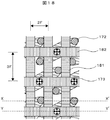
The layout of the memory cell formed by the above procedure is shown in FIGS.
FIG. 17 shows the
次に、図18には、ワード線181とソース線182が示されている。ソース線間隔はFを最小寸法とすると3Fである。また、ワード線間隔は2Fである。
さらに、図19には、ビット線191が示されている。ビット線間隔は3Fである。本実施例ではメモリセル面積を6F2にすることが出来る。下部電極BECのプラグ径は、例えば0.2F2〜2F2である。下部電極BECのプラグ径を1F2以下に加工する場合は、サイドウォールなどの段差をハードマスクとして利用し加工する方法などを用いることができる。
Next, FIG. 18 shows a
Further, FIG. 19 shows a
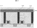
本実施例の要部断面模式図を図20と図21に示す。図20は図19中のX−X‘の断面模式図であり、図21は図19中のY−Y’の断面模式図である。図20では、サイドウォール201を利用して、ワード線202とBECの分離を行っていることが示されている。フィールド酸化膜203により、拡散層171は分離されている。
20 and 21 are schematic cross-sectional views of the relevant part of this example. 20 is a schematic cross-sectional view taken along line X-X ′ in FIG. 19, and FIG. 21 is a schematic cross-sectional view taken along line Y-Y ′ in FIG. 19. FIG. 20 shows that the
図21では、密着層214とプラグ材料213で形成された拡散層−ソース線接続部173がソース線182と拡散層171を接続していることが示されている。密着層214は例えばTiNであり、プラグ材料213は例えばWである。ともに、CVDで形成することが出来る。ソース線182はバリア層215と配線材料216により形成されている。バリア層としてはTa、配線材料としてはCuを用いることが出来る。
FIG. 21 shows that the diffusion layer-source
本実施例は、図13中のCu−Ta−O結晶化方法のうち、イオン閉じ込め層の結晶化をレーザー照射により行うことを特徴とする。
Cu−Ta−Oの成膜は以下のように行う。スパッタリング時の基盤温度はCu−Ta−Oが結晶化しない程度に低く制御し、アモルファスCu−Ta−Oを成膜する。次に、レーザー照射を用いたCu−Ta−Oの結晶化を行う。
This embodiment is characterized in that the ion confinement layer is crystallized by laser irradiation in the Cu-Ta-O crystallization method in FIG.
The film formation of Cu—Ta—O is performed as follows. The substrate temperature at the time of sputtering is controlled so low that Cu—Ta—O is not crystallized, and amorphous Cu—Ta—O is formed. Next, crystallization of Cu—Ta—O using laser irradiation is performed.
炉体を用いた熱処理ではなく、レーザー照射を行うことにより、シリコンウェハ基盤の温度の上昇を軽減することができる。これにより、拡散層中のドーパントが移動するため、トランジスタ特性が劣化する問題を回避することが出来るだけではなく、さらに、Low−k材料の劣化を防止することが出来るため、Low−k材料を層間絶縁膜に用いることが出来る。Low-k材料を用いることで、半導体回路の配線遅延を軽減することが可能になり、高速な動作を行うことが出来る。Low−k材料は一般的に耐熱性が低い。例えば、多孔性Low−k材料に400℃を超える熱負荷を与えると、内部の微細空隙が消滅し、誘電率kが上昇するため、配線遅延が増大したり、Low−k材料の変形により、配線ショートが生じたりする。Low−k材料が劣化する温度は、Low−k材料の種類により変化することは言うまでもない。 By performing laser irradiation instead of heat treatment using a furnace body, an increase in temperature of the silicon wafer substrate can be reduced. Thereby, since the dopant in the diffusion layer moves, not only the problem of deterioration of transistor characteristics can be avoided, but also the deterioration of the low-k material can be prevented. It can be used for an interlayer insulating film. By using the low-k material, it is possible to reduce the wiring delay of the semiconductor circuit and to perform high-speed operation. Low-k materials generally have low heat resistance. For example, when a thermal load exceeding 400 ° C. is applied to the porous Low-k material, the internal micro void disappears and the dielectric constant k increases, so that the wiring delay increases or the deformation of the Low-k material causes Wiring short circuit may occur. Needless to say, the temperature at which the low-k material deteriorates varies depending on the type of the low-k material.
レーザー照射方法を説明する。シリコンウェハ面と直行しウェハ中心を通る軸を中心にウェハを回転させ、レーザー照射部をウェハの半径方向に移動させる。また、レーザー照射部の位置により、回転速度を変化させ、レーザーの線速度を一定に保つ。上記により、均一な照射強度でのレーザー熱処理が可能である。 A laser irradiation method will be described. The wafer is rotated about an axis that is perpendicular to the silicon wafer surface and passes through the center of the wafer, and the laser irradiation unit is moved in the radial direction of the wafer. Further, the rotation speed is changed depending on the position of the laser irradiation unit, and the linear velocity of the laser is kept constant. By the above, laser heat treatment with uniform irradiation intensity is possible.
我々が測定したアモルファス状態のCu−Ta−Oの屈折率は、波長632.8nmにおいて、3.9であった。レーザー照射強度を16kW/mm2とし、レーザー照射部の移動速度を25mm/秒とし、レーザーの移動方向の照射長さを1μmとすることで、結晶化が可能であると考えられるが、Cu−Ta−O材料の組成により、屈折率や結晶化温度、結晶化に要する時間が変化するため、照射強度や照射部の移動速度を最適な値に制御することは言うまでもない。 The refractive index of amorphous Cu—Ta—O measured by us was 3.9 at a wavelength of 632.8 nm. It is considered that crystallization is possible by setting the laser irradiation intensity to 16 kW / mm 2 , the moving speed of the laser irradiation portion to 25 mm / second, and the irradiation length in the laser moving direction to 1 μm. Since the refractive index, the crystallization temperature, and the time required for crystallization change depending on the composition of the Ta—O material, it goes without saying that the irradiation intensity and the moving speed of the irradiated portion are controlled to optimum values.
また、レーザー照射によりCu−Ta−Oを選択的に加熱を行うことで結晶化させ、その下部に形成するCu−Ta−Sの温度上昇を抑えることが可能になる。その結果、Cu−Ta−Oの結晶化温度よりも耐熱性の低いCu−Ta−Sを用いて、Cu−Ta−SがCu−Ta−Oよりも下部にある構造を形成することが可能になる。 In addition, Cu—Ta—O is selectively heated by laser irradiation to be crystallized, and the temperature rise of Cu—Ta—S formed therebelow can be suppressed. As a result, it is possible to form a structure in which Cu-Ta-S is lower than Cu-Ta-O using Cu-Ta-S, which has lower heat resistance than the crystallization temperature of Cu-Ta-O. become.
本実施例は、図13中のCu−Ta−O結晶化方法のうち、アモルファスCu−Ta−O成膜後に電気炉もしくは赤外炉で熱処理を行い、Cu−Ta−Oを結晶化させることを特徴とする。時間をかけて結晶化を行うことにより、結晶成長の速度を抑え、相対的に結晶核生成の確率を高くすることが出来るため、微細な結晶構造が得られる。これにより、BEC上の粒界の数を均一化することができるため、粒界が書き換え動作に及ぼす影響を平均化することができる。その結果、ばらつきの少ない半導体回路装置を提供することが出来る。熱処理時間は例えば30分である。実施例1で述べたようにCu−Ta−Oの結晶化温度は600℃以上であるため、熱処理温度は600℃以上とするのが良い。 In this embodiment, among the Cu-Ta-O crystallization methods in FIG. 13, heat treatment is performed in an electric furnace or infrared furnace after amorphous Cu-Ta-O film formation to crystallize Cu-Ta-O. It is characterized by. By performing crystallization over time, the crystal growth rate can be suppressed and the probability of crystal nucleation can be relatively increased, so that a fine crystal structure can be obtained. Thereby, since the number of grain boundaries on the BEC can be made uniform, the influence of the grain boundaries on the rewriting operation can be averaged. As a result, a semiconductor circuit device with little variation can be provided. The heat treatment time is, for example, 30 minutes. As described in Example 1, since the crystallization temperature of Cu—Ta—O is 600 ° C. or higher, the heat treatment temperature is preferably 600 ° C. or higher.
本実施例は、記憶部の分離をCMPにより行うことを特徴とする。
本メモリの製造工程について、図22〜図24を用いて説明する。
まず、通常の半導体工程を用いてMISトランジスタ形成およびフィールド酸化膜による拡散層の分離を行う。次に層間絶縁膜形成後、上記トランジスタのドレインおよびソースに接続されたコンタクトホールを形成し、化学的気相成長法(CVD)により、密着層225および、プラグ材料224を形成する。その後、CMP(化学機械研磨)を行い、拡散層−1メタル線間接続部を形成する。次に、CVD成膜とダマシン加工を用いて、1メタル線223を形成する。1メタル線材料の例はWである。その後、エッチストッパ層221および層間絶縁膜226を形成し、さらに、CVDおよびドライエッチングを行い、段差部222を形成する。エッチストッパ層の材料の例はSiNであり、層間絶縁膜226の材料の例はPTEOSである。また、段差部222の材料の例はSiNである。結果として得られる断面の模式図を図22に示す。
This embodiment is characterized in that the storage unit is separated by CMP.
The manufacturing process of the memory will be described with reference to FIGS.
First, a MIS transistor is formed and a diffusion layer is separated by a field oxide film using a normal semiconductor process. Next, after forming an interlayer insulating film, contact holes connected to the drain and source of the transistor are formed, and an
さらに、イオン閉じ込め層11とイオン供給層12、上部電極15の成膜を行う。これらの成膜はすべてスパッタ法で行うことができる。但し、段差部の高さと開口部のアスペクト比が1を超える深穴を用いる場合は、CVD法を用いて各層の形成を行う。結果として得られる断面の模式図を図23に示す。
Further, the
次に、CMPを行うことで、図24に示される記憶部が分離された構造を形成することが出来る。本実施例を用いることで、特に微細なメモリセル構造を形成することが可能である。 Next, by performing CMP, a structure in which the memory portion shown in FIG. 24 is separated can be formed. By using this embodiment, a particularly fine memory cell structure can be formed.
以降、上部配線を形成することで、メモリ素子を製造する。なお、一般的な半導体プロセスを用いて本構造を形成するとCu−Ta−OもしくはCu−Ta−Sに10〜500nmの段差が生じる。
なお、本実施例では、ソース線がビット線の下部に配置されており、ソース線は1メタル線223を用いて配線されている。また、1メタル線と上部配線の接続部の形成を容易に行えるようにドライエッチストッパ層221を形成している。
Thereafter, the memory element is manufactured by forming the upper wiring. Note that when this structure is formed using a general semiconductor process, a step of 10 to 500 nm is formed in Cu—Ta—O or Cu—Ta—S.
In this embodiment, the source line is arranged below the bit line, and the source line is wired using one
11…イオン閉じ込め層、
12…イオン供給層、
13、213、224…プラグ材料、
14、214、225…密着層、
15、94…上部電極、
21…固体電解質層、
22…イオン供給源となる電極、
33…イオン、
34…金属、
51…ON動作、
52…OFF動作、
91、104…結晶Cu−Ta−O、
92…Cu−Ta−S、
93、103 PTEOS、
101…粒界、
102…粒内、
103…酸化シリコン、
121…層間絶縁膜、
141…ハードマスク、
142…レジスト、
171…拡散層、
172…下部電極、
173…ソース線−拡散層間接続部、
181…ワード線、
182…ソース線、
191…ビット線、
201…サイドウォール、
202…ワード線、
203…フィールド酸化膜、
215…バリア層、
216…配線材料、
221…エッチストッパ層、
222…段差部、
223…1メタル線、
RM…記憶部、
BEC…下部電極。
11 ... ion confinement layer,
12 ... Ion supply layer,
13, 213, 224 ... plug material,
14, 214, 225 ... adhesion layer,
15, 94 ... upper electrode,
21 ... Solid electrolyte layer,
22 ... Electrode serving as an ion source,
33 ... Ion,
34 ... metal,
51 ... ON operation,
52 ... OFF operation,
91, 104 ... Crystalline Cu-Ta-O,
92 ... Cu-Ta-S,
93, 103 PTEOS,
101 ... Grain boundary,
102 ... inside the grain,
103 ... silicon oxide,
121 ... interlayer insulating film,
141 ... Hard mask,
142 ... resist,
171 ... diffusion layer,
172 ... Lower electrode,
173 ... source line-diffusion interlayer connection,
181 ... Word line,
182 ... Source line,
191: Bit line,
201 ... sidewall,
202 ... word line,
203 ... Field oxide film,
215 ... barrier layer,
216 ... wiring material,
221 ... Etch stopper layer,
222 ... a step,
223 ... 1 metal wire,
RM ... storage unit,
BEC: Lower electrode.
Claims (20)
前記記録層の前記基盤側の一主面上に設けられた第1の電極と、
前記記録層の前記一主面に対向する他主面上に設けられた第2の電極とを備え、
前記記録層は、前記第1の電極に接する側に配置された第1層と前記第2の電極に接する側に配置された第2層との少なくとも2層より成り、
前記第1層は、Ag、Cu、Au、Znからなる群より選ばれた少なくとも1種類の元素と、Ta、W、Mo、Gdからなる群より選ばれた少なくとも1種類の元素と、酸素とを含んでなる結晶相であり、
前記第2層は、Ag、Cu、Au、Znからなる群より選ばれた少なくとも1種類の元素とS、Se、Teからなる群より選ばれた少なくとも1種類の元素を含むことを特徴とする半導体装置。 A recording layer for recording information by causing a change in electrical resistance provided on the substrate;
A first electrode provided on one principal surface of the base side of the recording layer;
A second electrode provided on the other main surface facing the one main surface of the recording layer,
The recording layer is composed of at least two layers of a first layer disposed on the side in contact with the first electrode and a second layer disposed on the side in contact with the second electrode,
The first layer includes at least one element selected from the group consisting of Ag, Cu, Au, and Zn, at least one element selected from the group consisting of Ta, W, Mo, and Gd, and oxygen. A crystal phase comprising
The second layer includes at least one element selected from the group consisting of Ag, Cu, Au, and Zn and at least one element selected from the group consisting of S, Se, and Te. Semiconductor device.
前記情報記憶部が前記請求項1に記載の半導体装置を有し、
前記情報記憶部へのパルス電圧印可により情報の書込み、または情報の読み取りを行うことを特徴とする半導体装置。 In a semiconductor memory device having a plurality of word lines and a plurality of memory cells including information storage units and selection elements provided at intersections of a plurality of bit lines intersecting the word lines via an insulating layer,
The information storage unit includes the semiconductor device according to claim 1,
A semiconductor device, wherein information is written or read by applying a pulse voltage to the information storage portion.
前記下部電極上に、Ag、Cu、Au、Znからなる群より選ばれた少なくとも1種類の元素と、Ta、W、Mo、Gdからなる群より選ばれた少なくとも1種類の元素と、酸素とを含む第1記憶層を形成し、さらに、前記第1記憶層上に、Ag、Cu、Au、Znからなる群より選ばれた少なくとも1種類の元素と、S、Se、Teからなる群より選ばれた少なくとも1種類の元素を含む第2記憶層を形成することにより前記第1記憶層および前記第2記憶層の少なくとも2層含んでなる記憶層を形成する工程と、
前記記録層上に上部電極を形成する工程と、を備え、
前記第1記憶層の形成後にアニールを行い、前記アニール後に前記第2記憶層を形成することを特徴とする半導体装置の製造方法。 Forming a lower electrode on the substrate;
On the lower electrode, at least one element selected from the group consisting of Ag, Cu, Au, Zn, at least one element selected from the group consisting of Ta, W, Mo, Gd, and oxygen A first memory layer including at least one element selected from the group consisting of Ag, Cu, Au, and Zn, and a group consisting of S, Se, and Te on the first memory layer. Forming a memory layer including at least two of the first memory layer and the second memory layer by forming a second memory layer containing at least one selected element;
Forming an upper electrode on the recording layer, and
A method of manufacturing a semiconductor device, wherein annealing is performed after the formation of the first memory layer, and the second memory layer is formed after the annealing.
前記アニール時の基盤温度が400℃以下であることを特徴とする請求項11に記載の半導体装置の製造方法。 Forming an interlayer insulating film on the substrate using a low-k material;
The method of manufacturing a semiconductor device according to claim 11, wherein a base temperature at the time of annealing is 400 ° C. or lower.
前記アニール時の基盤温度が400℃以下であることを特徴とする請求項17に記載の半導体装置の製造方法。 Forming an interlayer insulating film on the substrate using a low-k material;
The method of manufacturing a semiconductor device according to claim 17, wherein a base temperature at the time of annealing is 400 ° C. or lower.
前記下部電極上に、Ag、Cu、Au、Znからなる群より選ばれた少なくとも1種類の元素と、S、Se、Teからなる群より選ばれた少なくとも1種類の元素を含む第1記憶層を形成し、さらに、前記第1記憶層上に、Ag、Cu、Au、Znからなる群より選ばれた少なくとも1種類の元素と、Ta、W、Mo、Gdからなる群より選ばれた少なくとも1種類の元素と、酸素とを含む結晶相からなる第2記憶層とを形成することにより前記第1記憶層および前記第2記憶層の少なくとも2層含んでなる記憶層を形成する工程と、
前記記録層上に上部電極を形成する工程とを有すること特徴とする半導体装置の製造方法。 Forming a lower electrode on the substrate;
A first memory layer including at least one element selected from the group consisting of Ag, Cu, Au, and Zn and at least one element selected from the group consisting of S, Se, Te on the lower electrode. And at least one element selected from the group consisting of Ag, Cu, Au, Zn, and at least selected from the group consisting of Ta, W, Mo, Gd on the first memory layer Forming a memory layer including at least two of the first memory layer and the second memory layer by forming a second memory layer made of a crystal phase containing one kind of element and oxygen;
And a step of forming an upper electrode on the recording layer.
Priority Applications (4)
| Application Number | Priority Date | Filing Date | Title |
|---|---|---|---|
| JP2008089776A JP2009246085A (en) | 2008-03-31 | 2008-03-31 | Semiconductor device, and method of manufacturing the same |
| TW098101094A TW201001693A (en) | 2008-03-31 | 2009-01-13 | Semiconductor device and method of manufacturing the same |
| US12/370,417 US20090242868A1 (en) | 2008-03-31 | 2009-02-12 | Semiconductor device and method of manufacturing the same |
| CNA2009100071701A CN101552321A (en) | 2008-03-31 | 2009-02-13 | Semiconductor device and method of manufacturing the same |
Applications Claiming Priority (1)
| Application Number | Priority Date | Filing Date | Title |
|---|---|---|---|
| JP2008089776A JP2009246085A (en) | 2008-03-31 | 2008-03-31 | Semiconductor device, and method of manufacturing the same |
Publications (1)
| Publication Number | Publication Date |
|---|---|
| JP2009246085A true JP2009246085A (en) | 2009-10-22 |
Family
ID=41115710
Family Applications (1)
| Application Number | Title | Priority Date | Filing Date |
|---|---|---|---|
| JP2008089776A Withdrawn JP2009246085A (en) | 2008-03-31 | 2008-03-31 | Semiconductor device, and method of manufacturing the same |
Country Status (4)
| Country | Link |
|---|---|
| US (1) | US20090242868A1 (en) |
| JP (1) | JP2009246085A (en) |
| CN (1) | CN101552321A (en) |
| TW (1) | TW201001693A (en) |
Cited By (9)
| Publication number | Priority date | Publication date | Assignee | Title |
|---|---|---|---|---|
| JP2011096714A (en) * | 2009-10-27 | 2011-05-12 | Nara Institute Of Science & Technology | Resistive random access memory having metal nano particle |
| WO2011092993A1 (en) * | 2010-02-01 | 2011-08-04 | 学校法人 龍谷大学 | Oxide film, process for producing same, target, and process for producing sintered oxide |
| JP2012084706A (en) * | 2010-10-13 | 2012-04-26 | Sony Corp | Nonvolatile memory element, nonvolatile memory element group and manufacturing method of the same |
| JP2012084765A (en) * | 2010-10-14 | 2012-04-26 | Sony Corp | Nonvolatile memory element and method for manufacturing the same |
| WO2012074131A1 (en) * | 2010-12-03 | 2012-06-07 | 日本電気株式会社 | Semiconductor device and production method for same |
| WO2012105139A1 (en) * | 2011-02-02 | 2012-08-09 | 日本電気株式会社 | Switching element, semiconductor device, and methods for manufacturing switching element and semiconductor device |
| JP2013026514A (en) * | 2011-07-22 | 2013-02-04 | Sony Corp | Storage device and manufacturing method thereof |
| WO2014103691A1 (en) * | 2012-12-25 | 2014-07-03 | ソニー株式会社 | Storage element and storage device |
| JP2017034223A (en) * | 2015-08-03 | 2017-02-09 | 華邦電子股▲ふん▼有限公司 | Resistance change type memory |
Families Citing this family (10)
| Publication number | Priority date | Publication date | Assignee | Title |
|---|---|---|---|---|
| KR100983175B1 (en) * | 2008-07-03 | 2010-09-20 | 광주과학기술원 | Resistance RAM having oxide layer and solid electrolyte layer, and method for operating the same |
| KR20110008553A (en) * | 2009-07-20 | 2011-01-27 | 삼성전자주식회사 | Semiconductor memory device and method of forming the same |
| JP5692085B2 (en) * | 2009-11-11 | 2015-04-01 | 日本電気株式会社 | Resistance change element, semiconductor device, and method of forming resistance change element |
| JP5548170B2 (en) | 2011-08-09 | 2014-07-16 | 株式会社東芝 | Resistance change memory and manufacturing method thereof |
| JP5684104B2 (en) | 2011-12-27 | 2015-03-11 | 株式会社東芝 | Method for manufacturing metal bridge type memory device |
| WO2014087784A1 (en) * | 2012-12-03 | 2014-06-12 | ソニー株式会社 | Memory element and memory device |
| JP6213559B2 (en) * | 2013-03-18 | 2017-10-18 | 富士通株式会社 | Electronic device, manufacturing method thereof, and network system |
| US8981334B1 (en) * | 2013-11-01 | 2015-03-17 | Micron Technology, Inc. | Memory cells having regions containing one or both of carbon and boron |
| CN108950507B (en) * | 2018-08-15 | 2020-03-17 | 电子科技大学 | Memristive switching device based on a-TSC-O ceramic film and preparation method thereof |
| CN112002801B (en) * | 2020-07-20 | 2021-09-07 | 厦门半导体工业技术研发有限公司 | Semiconductor device and method for manufacturing semiconductor device |
Family Cites Families (8)
| Publication number | Priority date | Publication date | Assignee | Title |
|---|---|---|---|---|
| JP4119950B2 (en) * | 2000-09-01 | 2008-07-16 | 独立行政法人科学技術振興機構 | Electronic device capable of controlling conductance |
| JP4190238B2 (en) * | 2002-09-13 | 2008-12-03 | 株式会社ルネサステクノロジ | Nonvolatile semiconductor memory device |
| JP4792714B2 (en) * | 2003-11-28 | 2011-10-12 | ソニー株式会社 | Storage element and storage device |
| JP2006319028A (en) * | 2005-05-11 | 2006-11-24 | Nec Corp | Switching element, rewritable logic integrated circuit, and memory element |
| JP2009021436A (en) * | 2007-07-12 | 2009-01-29 | Hitachi Ltd | Semiconductor device |
| JP5227544B2 (en) * | 2007-07-12 | 2013-07-03 | 株式会社日立製作所 | Semiconductor device |
| TWI402980B (en) * | 2007-07-20 | 2013-07-21 | Macronix Int Co Ltd | Resistive memory structure with buffer layer |
| JP2009043905A (en) * | 2007-08-08 | 2009-02-26 | Hitachi Ltd | Semiconductor device |
-
2008
- 2008-03-31 JP JP2008089776A patent/JP2009246085A/en not_active Withdrawn
-
2009
- 2009-01-13 TW TW098101094A patent/TW201001693A/en unknown
- 2009-02-12 US US12/370,417 patent/US20090242868A1/en not_active Abandoned
- 2009-02-13 CN CNA2009100071701A patent/CN101552321A/en active Pending
Cited By (16)
| Publication number | Priority date | Publication date | Assignee | Title |
|---|---|---|---|---|
| JP2011096714A (en) * | 2009-10-27 | 2011-05-12 | Nara Institute Of Science & Technology | Resistive random access memory having metal nano particle |
| CN102741448A (en) * | 2010-02-01 | 2012-10-17 | 学校法人龙谷大学 | Oxide film, process for producing same, target, and process for producing sintered oxide |
| WO2011092993A1 (en) * | 2010-02-01 | 2011-08-04 | 学校法人 龍谷大学 | Oxide film, process for producing same, target, and process for producing sintered oxide |
| JP2012084706A (en) * | 2010-10-13 | 2012-04-26 | Sony Corp | Nonvolatile memory element, nonvolatile memory element group and manufacturing method of the same |
| US8952348B2 (en) | 2010-10-13 | 2015-02-10 | Sony Corporation | Nonvolatile memory device, nonvolatile memory device group, and manufacturing method thereof |
| JP2012084765A (en) * | 2010-10-14 | 2012-04-26 | Sony Corp | Nonvolatile memory element and method for manufacturing the same |
| JPWO2012074131A1 (en) * | 2010-12-03 | 2014-05-19 | 日本電気株式会社 | Semiconductor device and manufacturing method thereof |
| WO2012074131A1 (en) * | 2010-12-03 | 2012-06-07 | 日本電気株式会社 | Semiconductor device and production method for same |
| WO2012105139A1 (en) * | 2011-02-02 | 2012-08-09 | 日本電気株式会社 | Switching element, semiconductor device, and methods for manufacturing switching element and semiconductor device |
| JP5807789B2 (en) * | 2011-02-02 | 2015-11-10 | 日本電気株式会社 | Switching element, semiconductor device and manufacturing method thereof |
| JP2013026514A (en) * | 2011-07-22 | 2013-02-04 | Sony Corp | Storage device and manufacturing method thereof |
| WO2014103691A1 (en) * | 2012-12-25 | 2014-07-03 | ソニー株式会社 | Storage element and storage device |
| JPWO2014103691A1 (en) * | 2012-12-25 | 2017-01-12 | ソニー株式会社 | Storage element and storage device |
| US10418416B2 (en) | 2012-12-25 | 2019-09-17 | Sony Semiconductor Solutions Corporation | Memory device and memory unit |
| US10879312B2 (en) | 2012-12-25 | 2020-12-29 | Sony Corporation | Memory device and memory unit |
| JP2017034223A (en) * | 2015-08-03 | 2017-02-09 | 華邦電子股▲ふん▼有限公司 | Resistance change type memory |
Also Published As
| Publication number | Publication date |
|---|---|
| US20090242868A1 (en) | 2009-10-01 |
| CN101552321A (en) | 2009-10-07 |
| TW201001693A (en) | 2010-01-01 |
Similar Documents
| Publication | Publication Date | Title |
|---|---|---|
| JP2009246085A (en) | Semiconductor device, and method of manufacturing the same | |
| US7804083B2 (en) | Phase change memory cell including a thermal protect bottom electrode and manufacturing methods | |
| JP5688196B2 (en) | Ultra-thin multi-layer phase change memory device | |
| TWI331793B (en) | Method of manufacturing a pipe shaped phase change memory | |
| US7675053B2 (en) | Memory device comprising a memory layer and a metal chalcogenide ion-source layer | |
| TWI442518B (en) | Self aligning pillar memory cell device and method for making the same | |
| JP6062155B2 (en) | Ge-rich GST-212 phase change material | |
| US8084760B2 (en) | Ring-shaped electrode and manufacturing method for same | |
| US7569844B2 (en) | Memory cell sidewall contacting side electrode | |
| WO2011043448A1 (en) | Semiconductor device and method for manufacturing same | |
| JP4396621B2 (en) | Storage element and storage device | |
| TWI489591B (en) | Fill-in etching free pore device | |
| TWI385790B (en) | Polysilicon plug bipolar transistor for phase change memory | |
| JP4715320B2 (en) | Storage element and storage device | |
| JP2006173267A (en) | Storage element and storage device | |
| TW201011909A (en) | Storage element and storage device | |
| JP2009206418A (en) | Nonvolatile memory device and manufacturing method for the same | |
| JP4934276B2 (en) | Semiconductor memory and manufacturing method thereof | |
| JP4465969B2 (en) | Semiconductor memory element and semiconductor memory device using the same | |
| JPWO2010140210A1 (en) | Semiconductor memory device and manufacturing method thereof | |
| WO2014103691A1 (en) | Storage element and storage device | |
| US20230413696A1 (en) | Diffusion barrier layer in programmable metallization cell | |
| US7985693B2 (en) | Method of producing phase change memory device | |
| JP2010087008A (en) | Nonvolatile memory device and method of manufacturing the same | |
| KR20090104643A (en) | Semiconductor device and method thereof |
Legal Events
| Date | Code | Title | Description |
|---|---|---|---|
| A621 | Written request for application examination |
Free format text: JAPANESE INTERMEDIATE CODE: A621 Effective date: 20100729 |
|
| A761 | Written withdrawal of application |
Free format text: JAPANESE INTERMEDIATE CODE: A761 Effective date: 20110404 |