JP2009200321A - Light-emitting device and its manufacturing method - Google Patents
Light-emitting device and its manufacturing method Download PDFInfo
- Publication number
- JP2009200321A JP2009200321A JP2008041637A JP2008041637A JP2009200321A JP 2009200321 A JP2009200321 A JP 2009200321A JP 2008041637 A JP2008041637 A JP 2008041637A JP 2008041637 A JP2008041637 A JP 2008041637A JP 2009200321 A JP2009200321 A JP 2009200321A
- Authority
- JP
- Japan
- Prior art keywords
- light emitting
- inner lead
- light
- emitting device
- lead
- Prior art date
- Legal status (The legal status is an assumption and is not a legal conclusion. Google has not performed a legal analysis and makes no representation as to the accuracy of the status listed.)
- Pending
Links
Images


Classifications
-
- H—ELECTRICITY
- H01—ELECTRIC ELEMENTS
- H01L—SEMICONDUCTOR DEVICES NOT COVERED BY CLASS H10
- H01L2224/00—Indexing scheme for arrangements for connecting or disconnecting semiconductor or solid-state bodies and methods related thereto as covered by H01L24/00
- H01L2224/01—Means for bonding being attached to, or being formed on, the surface to be connected, e.g. chip-to-package, die-attach, "first-level" interconnects; Manufacturing methods related thereto
- H01L2224/26—Layer connectors, e.g. plate connectors, solder or adhesive layers; Manufacturing methods related thereto
- H01L2224/31—Structure, shape, material or disposition of the layer connectors after the connecting process
- H01L2224/32—Structure, shape, material or disposition of the layer connectors after the connecting process of an individual layer connector
- H01L2224/321—Disposition
- H01L2224/32151—Disposition the layer connector connecting between a semiconductor or solid-state body and an item not being a semiconductor or solid-state body, e.g. chip-to-substrate, chip-to-passive
- H01L2224/32221—Disposition the layer connector connecting between a semiconductor or solid-state body and an item not being a semiconductor or solid-state body, e.g. chip-to-substrate, chip-to-passive the body and the item being stacked
- H01L2224/32245—Disposition the layer connector connecting between a semiconductor or solid-state body and an item not being a semiconductor or solid-state body, e.g. chip-to-substrate, chip-to-passive the body and the item being stacked the item being metallic
-
- H—ELECTRICITY
- H01—ELECTRIC ELEMENTS
- H01L—SEMICONDUCTOR DEVICES NOT COVERED BY CLASS H10
- H01L2224/00—Indexing scheme for arrangements for connecting or disconnecting semiconductor or solid-state bodies and methods related thereto as covered by H01L24/00
- H01L2224/01—Means for bonding being attached to, or being formed on, the surface to be connected, e.g. chip-to-package, die-attach, "first-level" interconnects; Manufacturing methods related thereto
- H01L2224/42—Wire connectors; Manufacturing methods related thereto
- H01L2224/47—Structure, shape, material or disposition of the wire connectors after the connecting process
- H01L2224/48—Structure, shape, material or disposition of the wire connectors after the connecting process of an individual wire connector
- H01L2224/481—Disposition
- H01L2224/48151—Connecting between a semiconductor or solid-state body and an item not being a semiconductor or solid-state body, e.g. chip-to-substrate, chip-to-passive
- H01L2224/48221—Connecting between a semiconductor or solid-state body and an item not being a semiconductor or solid-state body, e.g. chip-to-substrate, chip-to-passive the body and the item being stacked
- H01L2224/48245—Connecting between a semiconductor or solid-state body and an item not being a semiconductor or solid-state body, e.g. chip-to-substrate, chip-to-passive the body and the item being stacked the item being metallic
- H01L2224/48247—Connecting between a semiconductor or solid-state body and an item not being a semiconductor or solid-state body, e.g. chip-to-substrate, chip-to-passive the body and the item being stacked the item being metallic connecting the wire to a bond pad of the item
-
- H—ELECTRICITY
- H01—ELECTRIC ELEMENTS
- H01L—SEMICONDUCTOR DEVICES NOT COVERED BY CLASS H10
- H01L2224/00—Indexing scheme for arrangements for connecting or disconnecting semiconductor or solid-state bodies and methods related thereto as covered by H01L24/00
- H01L2224/01—Means for bonding being attached to, or being formed on, the surface to be connected, e.g. chip-to-package, die-attach, "first-level" interconnects; Manufacturing methods related thereto
- H01L2224/42—Wire connectors; Manufacturing methods related thereto
- H01L2224/47—Structure, shape, material or disposition of the wire connectors after the connecting process
- H01L2224/48—Structure, shape, material or disposition of the wire connectors after the connecting process of an individual wire connector
- H01L2224/484—Connecting portions
- H01L2224/48463—Connecting portions the connecting portion on the bonding area of the semiconductor or solid-state body being a ball bond
- H01L2224/48465—Connecting portions the connecting portion on the bonding area of the semiconductor or solid-state body being a ball bond the other connecting portion not on the bonding area being a wedge bond, i.e. ball-to-wedge, regular stitch
-
- H—ELECTRICITY
- H01—ELECTRIC ELEMENTS
- H01L—SEMICONDUCTOR DEVICES NOT COVERED BY CLASS H10
- H01L2224/00—Indexing scheme for arrangements for connecting or disconnecting semiconductor or solid-state bodies and methods related thereto as covered by H01L24/00
- H01L2224/73—Means for bonding being of different types provided for in two or more of groups H01L2224/10, H01L2224/18, H01L2224/26, H01L2224/34, H01L2224/42, H01L2224/50, H01L2224/63, H01L2224/71
- H01L2224/732—Location after the connecting process
- H01L2224/73251—Location after the connecting process on different surfaces
- H01L2224/73265—Layer and wire connectors
-
- H—ELECTRICITY
- H01—ELECTRIC ELEMENTS
- H01L—SEMICONDUCTOR DEVICES NOT COVERED BY CLASS H10
- H01L2924/00—Indexing scheme for arrangements or methods for connecting or disconnecting semiconductor or solid-state bodies as covered by H01L24/00
- H01L2924/013—Alloys
- H01L2924/0132—Binary Alloys
- H01L2924/01322—Eutectic Alloys, i.e. obtained by a liquid transforming into two solid phases
Landscapes
- Led Device Packages (AREA)
Abstract
Description
本発明は、発光装置及びその製造方法に関する。 The present invention relates to a light emitting device and a method for manufacturing the same.
照明、車載、信号機などの用途における半導体発光装置は、高出力かつ小型であることが要求される。また、動作温度範囲が広いなど使用条件が厳しくなるに伴い高い機械的強度を有するパッケージが必要となる。さらに、ESD(electrostatic discharge:静電気放電)耐量高め信頼性を改善することが要求される。 Semiconductor light emitting devices for applications such as lighting, in-vehicle use, and traffic lights are required to have high output and small size. In addition, a package having high mechanical strength is required as usage conditions become severe, such as a wide operating temperature range. Furthermore, it is required to increase the ESD (electrostatic discharge) resistance and improve the reliability.
パッケージを構成する樹脂成型体に設けられた凹部の内側側壁を光反射面とし、発光素子の側方へ放出される光を上方に反射すると光出力を高めることが容易になる。しかし、樹脂成型体の凹部底面に発光素子及びESD耐量を高める保護素子を配置しようとすると、発光素子と光反射面との距離が長くなり、パッケージの平面サイズが大きくなり、かつ光取り出し効率が低下する。 If the inner side wall of the recess provided in the molded resin constituting the package is used as a light reflecting surface and the light emitted to the side of the light emitting element is reflected upward, the light output can be easily increased. However, if an attempt is made to arrange a light emitting element and a protective element for increasing ESD resistance on the bottom surface of the concave portion of the resin molded body, the distance between the light emitting element and the light reflecting surface becomes longer, the planar size of the package becomes larger, and the light extraction efficiency is improved. descend.
静電気放電衝撃に対する保護機能が内蔵された高輝度発光ダイオードに関する技術開示例がある(特許文献1)。この技術開示例では、リードフレームの上面にLEDチップを実装し、リードフレームの下面に静電気放電衝撃保護素子を備えている。
しかしながら、この技術開示例では、高出力を得ることが容易ではなく、またリードフレームの上面及び下面の両側にチップを配置するために、パッケージの薄型化が困難である。
However, in this technology disclosure example, it is not easy to obtain a high output, and it is difficult to reduce the thickness of the package because chips are arranged on both sides of the upper surface and the lower surface of the lead frame.
パッケージの小型化及び薄型化が容易で、高出力化が可能な保護素子内蔵型の発光装置及びその製造方法を提供する。 Provided are a light-emitting device with a built-in protection element, which can easily reduce the size and thickness of a package and can achieve high output, and a method for manufacturing the same.
本発明の一態様によれば、開口端に向かって拡開し内部側壁が光反射面である凹部を有し、樹脂からなる成型体と、前記成型体に埋め込まれ且つその一部が前記凹部の中に露出した第1のインナーリード部を有する、第1のリードと、前記凹部の中に露出した前記第1のインナーリード部の上面に接着された発光素子と、前記成型体に埋め込まれ且つその一部が前記凹部の中に露出した第2のインナーリード部を有し、前記第2のインナーリード部の先端部が前記第1のインナーリード部の先端部と対向する、第2のリードと、前記第1のインナーリード部の前記上面及び前記上面と同一の側である前記第2のインナーリード部の上面のいずれかに接着され、前記成型体に埋め込まれた保護素子と、を備えたことを特徴とする発光装置が提供される。 According to one aspect of the present invention, there is a concave portion that is widened toward the opening end and whose inner side wall is a light reflecting surface, and is formed of a resin, embedded in the molded body, and part of the concave portion. A first lead having a first inner lead portion exposed in the light emitting element, a light emitting element bonded to an upper surface of the first inner lead portion exposed in the concave portion, and embedded in the molded body. And a second inner lead portion that is partly exposed in the recess, and a tip portion of the second inner lead portion is opposed to a tip portion of the first inner lead portion. A lead and a protective element that is bonded to either the upper surface of the first inner lead portion or the upper surface of the second inner lead portion that is on the same side as the upper surface, and embedded in the molded body; Provided with a light-emitting device characterized by comprising It is.
また、本発明の他の一態様によれば、上記発光装置の製造方法であって、前記第1及び第2のリードを有するリードフレームの上面に前記保護素子を接着する工程と、前記第1のインナーリード部のうちの前記発光素子の接着領域が前記凹部の中に露出し、前記保護素子と、前記第1及び第2のインナーリード部の一部と、が埋め込まれるように、前記樹脂を用いて前記成型体を形成する工程と、を備えたことを特徴とする発光装置の製造方法が提供される。 According to another aspect of the present invention, in the method for manufacturing the light emitting device, the step of bonding the protective element to the upper surface of a lead frame having the first and second leads, and the first In the inner lead portion, the resin region is exposed so that the adhesive region of the light emitting element is exposed in the recess, and the protection element and a part of the first and second inner lead portions are embedded. And a step of forming the molded body by using a light emitting device.
また、本発明のさらに他の一態様によれば、上記発光装置の製造方法であって、前記第1及び第2のリードを有するリードフレームの上面に、前記樹脂として用いる熱可塑性樹脂のガラス転移温度よりも高い融点を有する第1の金属半田を用いて前記保護素子を接着する工程と、前記リードフレームの前記上面に、前記ガラス転移温度よりも高い融点を有する第2の金属半田を用いて前記発光素子を接着する工程と、前記発光素子が前記凹部の中に露出し、前記保護素子と、前記第1及び第2のインナーリード部の一部と、が埋め込まれるように、前記熱可塑性樹脂を用いて前記成型体を形成する工程と、を備えたことを特徴とする発光装置の製造方法が提供される。 According to yet another aspect of the present invention, there is provided a method for manufacturing the light emitting device, wherein a glass transition of a thermoplastic resin used as the resin on an upper surface of a lead frame having the first and second leads. Bonding the protective element using a first metal solder having a melting point higher than the temperature; and using a second metal solder having a melting point higher than the glass transition temperature on the upper surface of the lead frame. Bonding the light emitting element; and exposing the thermoplastic element so that the light emitting element is exposed in the recess and the protection element and part of the first and second inner lead portions are embedded. And a step of forming the molded body using a resin. A method of manufacturing a light emitting device is provided.
パッケージの小型化及び薄型化が容易で、高出力化が可能な保護素子内蔵型の発光装置及びその製造方法が提供される。 Provided are a light-emitting device with a built-in protection element, which can easily reduce the size and thickness of a package and can achieve high output, and a method for manufacturing the same.
以下、図面を参照しつつ本発明の実施の形態について説明する。
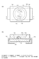
図1は、本発明の第1の実施形態にかかる発光装置を表す。すなわち、図1(a)は、模式平面図、図1(b)はA−A線に沿った模式断面図、図1(c)はB−B線に沿った模式断面図である。紫外〜可視光の波長を放出する発光素子10が、第1のリード22のインナーリード22a上に接着剤11を用いて接着(マウント)されている。
Hereinafter, embodiments of the present invention will be described with reference to the drawings.
FIG. 1 shows a light emitting device according to a first embodiment of the present invention. 1A is a schematic plan view, FIG. 1B is a schematic cross-sectional view along the line AA, and FIG. 1C is a schematic cross-sectional view along the line BB. The
第1のリード22は、樹脂に埋め込まれたインナーリード部22aと、樹脂から突出したアウターリード部22bと、を有している。また、第2のリード32は、樹脂に埋め込まれたインナーリード部32aと、樹脂から突出したアウターリード部32bと、を有しており、インナーリード部22aの先端部と、インナーリード部32bの先端部と、が熱可塑性樹脂からなる成型体40の内部で互いに対向している。発光素子10の上部の電極(図示せず)と、第2のリード32のインナーリード部32aと、がボンディングワイヤ15により接続されている。
The
第2のリード32のインナーリード部32aの上には保護素子12が、接着剤13を用いてマウントされており、保護素子12の上部電極(図示せず)と、第1のリード22のインナーリード部22aと、がボンディングワイヤ14により接続されている。保護素子12は、発光素子10がESDや逆方向印加電圧により破壊することを抑制するもので、ダイオードやバリスタなどを用いることができる。
The
例えば、保護素子12がダイオードの場合、発光素子10とはpn接合の方向が互いに逆方向となるように、発光素子10と保護素子12とを接続する。図1において、発光素子10と保護素子12とは基板側が同一の極性を有しているが、発光素子10の基板極性と保護素子12の基板極性が逆であれば、保護素子12を第1のリード22にマウントすればよい。発光素子10のpn接合に逆方向電圧が印加されると、保護素子12を介して電流が流れ、発光素子10に過大な逆方向電流が流れることを抑制し、発光素子10の破壊を防止できる。
For example, when the
さらに、保護素子12を定電圧ダイオード(ツェナーダイオイード)とすると、ESD及び誤動作による高電圧が印加されても、ツェナー電圧以上の電圧ではツェナーダイオードを介して電流が流れるので発光素子10の破壊を防止できより好ましい。
Furthermore, when the
他方、バリスタは半導体セラミックからなり、2つの電極間における非直線性抵抗特性を利用してESDによるサージ電圧を吸収し、発光素子10を保護できる。
On the other hand, the varistor is made of a semiconductor ceramic, and can absorb the surge voltage due to ESD using the non-linear resistance characteristic between the two electrodes to protect the
発光素子10は、AlGaAs系、GaAs系、InGaAlP系、InGaAlN系などからなる発光層を含み、紫外〜赤外光の波長帯の光を放出することができる。封止樹脂42に、蛍光体を分散して配置すると、発光素子10からの光の波長変換光を生成し、発光素子10からの放出光と、波長変換光と、を混合し、例えば白色光を得ることができる。
The
第1及び第2のリード22、32を有するリードフレームの材料には銅系または鉄系の合金を用いることができるが、銅系材料は高い熱伝導率であるのでより好ましい。第1及び第2のリード22、23の厚さは、例えば0.1〜2.0mmの間とすることができる。第1及び第2のリード22、23の表面にメッキなどによりコーティングを施すと、インナーリード22a、32aにおいて光反射率を高め、また、アウターリード22b、32bにおいて実装基板との間で半田の接合強度をあげることができる。コーティングとしては、例えば、銀、ニッケル/パラジウム/金をこの順序に積層したものなどとすることができる。銀の場合、例えば厚さを1〜10μmなどとする。
A copper-based or iron-based alloy can be used as the material of the lead frame having the first and second leads 22, 32, but a copper-based material is more preferable because of its high thermal conductivity. The thickness of the first and second leads 22 and 23 can be, for example, between 0.1 and 2.0 mm. When the surface of the first and second leads 22 and 23 is coated by plating or the like, the light reflectivity is increased in the
第1及び第2のリード22、32、及び保護素子12は、熱可塑性樹脂などの樹脂からなる成型体40に埋め込まれている。すなわち、インナーリード22a、32aは、発光素子10及び保護素子12のマウント領域、ボンディングワイヤの接続領域を除いて成型体40に埋め込まれている。なお、樹脂としては、エポキシからなる熱硬化性樹脂などを用いることもできる。
The first and second leads 22 and 32 and the
成型体40は、開口端に向かって拡開する凹部40aを有し、凹部40aの底面40cには発光素子10が配置される。また、凹部40の内部側壁40bは傾斜しており、発光素子10からの放出光を上方に向かって反射する光反射面となる。
The molded
なお、本明細書において、熱可塑性樹脂とは、加熱すると軟化さらには液状化し、冷却すると固化し、これを繰り返すことができる高分子物質をいう。図2は、熱可塑性樹脂のガラス転移温度を説明する図である。加熱によりガラス状からゴム状に軟化し弾性率が低下し始める温度Tg1をガラス転移温度と定義する。実線で表す非晶性樹脂の場合、ガラス転移温度Tg1よりも低い固化した状態においても、高分子配列が不規則となっている。非晶性樹脂では、ガラス転移温度が高い程、耐熱性に優れていると言える。 In this specification, a thermoplastic resin refers to a polymer substance that can be softened and liquefied when heated, solidified when cooled, and repeated. FIG. 2 is a view for explaining the glass transition temperature of the thermoplastic resin. The temperature Tg1 at which the elastic modulus begins to decrease due to softening from glass to rubber by heating is defined as the glass transition temperature. In the case of an amorphous resin represented by a solid line, the polymer arrangement is irregular even in a solidified state lower than the glass transition temperature Tg1. In an amorphous resin, it can be said that the higher the glass transition temperature, the better the heat resistance.
他方、鎖線で表す結晶性樹脂の場合、融点Tm1はガラス転移温度Tg2よりも高く、この融点Tm1よりも低い温度範囲において高分子配列が規則正しい。結晶性樹脂では、融点Tm1が高い程、耐熱性に優れていると言える。 On the other hand, in the case of a crystalline resin represented by a chain line, the melting point Tm1 is higher than the glass transition temperature Tg2, and the polymer arrangement is regular in a temperature range lower than the melting point Tm1. It can be said that the higher the melting point Tm1, the better the heat resistance of the crystalline resin.
熱可塑性樹脂の材料としては、ガラス転移温度が100℃以上であり、引っ張り強度が49MPa以上、曲げ弾性率が2.4GPa以上の特性を有するエンジニアリング樹脂などが好ましい。 As the thermoplastic resin material, an engineering resin having a glass transition temperature of 100 ° C. or higher, a tensile strength of 49 MPa or higher, and a flexural modulus of 2.4 GPa or higher is preferable.
エンジニアリング樹脂として、ポリアミド(PA)、ポリアセタール(POM)、ポリイミド(PI)、ポリアミドイミド(PAI)、ポリケトン(PK)、ポリカーボネート(PC)、ポリフェニレンサルファイド(PPS)、ポリフタルアミド(PPA)などの材料がある。なお、PA、POMなどは結晶性樹脂であり、PCは非晶性樹脂である。 Materials such as polyamide (PA), polyacetal (POM), polyimide (PI), polyamideimide (PAI), polyketone (PK), polycarbonate (PC), polyphenylene sulfide (PPS), polyphthalamide (PPA) as engineering resins There is. PA and POM are crystalline resins, and PC is an amorphous resin.
成型体40の材料としては、200℃以上の耐熱性を有するPPAなどの材料を用いることができる。これらの熱可塑性樹脂にガラス繊維を混合すると、機械的強度がさらに高められたパッケージとできるのでより好ましい。
As a material of the molded
また、熱可塑性樹脂には、例えばチタン酸カリウムの粉末などを混合しておくと、凹部40aの内部側壁40bを光反射面とし、光取り出し効率を改善することができる。
なお、内部側壁40bに、Ag、Al、Au、これらの合金などを、例えば蒸着法などを用いて形成し、光反射面とすることができる。
In addition, when the thermoplastic resin is mixed with, for example, potassium titanate powder, the
In addition, Ag, Al, Au, these alloys, etc. can be formed in the
図3は、第1の実施形態にかかる発光装置の製造方法を表すフローチャートである。また、図4はこの製造方法の工程断面図である。通常、リードフレームは数十〜数百個が連結された多数個取りとなっている。図4(a)のように、リードフレームを構成する第2のリード32の上面32cに、保護素子12を接着剤13を用いてマウントする。接着剤13には、例えば銀ペーストのような導電性接着剤を用いる。銀ペーストの場合、塗布後約200℃で熱硬化を行う。導電性接着剤を用いる場合、接着工程の接着温度は熱硬化温度と略同一である。接着剤13として、AuSn(融点約280℃)、AuSi(融点約370℃)のような金属半田を用いることもでき、この場合、接着温度は金属半田の融点と略同一である。さらに保護素子12の上部電極(図示せず)と、リードフレームを構成する第1のリード22と、をボンディングワイヤ14を用いて接続する(S100)。
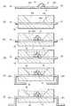
FIG. 3 is a flowchart showing a method for manufacturing the light emitting device according to the first embodiment. FIG. 4 is a process sectional view of this manufacturing method. Usually, a large number of lead frames are connected by connecting several tens to several hundreds. As shown in FIG. 4A, the
インナーリード部22a、32aは、発光素子10のマウント領域及びボンディングワイヤ15の接続領域を除き、金型を用いて樹脂のインサート成型により埋め込まれる。この場合、図4(b)のように、成型体40は、凹部40aを形成し、保護素子12を埋め込むような金型を用いて形成される(S102)。このインサート成型工程において、例えば金型温度を約150℃、樹脂温度を約300℃とする。
The
続いて、図4(c)のように、第1のリード22の上面22cに導電性接着剤及び金属半田などの接着剤11などを用いて発光素子10を接着し、ボンディングワイヤ15により第2のリード32の露出している領域と接続する(S104)。
Subsequently, as shown in FIG. 4C, the
続いて、図4(d)のように、液状の封止樹脂42を撹拌脱泡し、ポッティング法などを用い成型体40の凹部40aに充填し、約200℃で熱硬化する(S106)。封止樹脂42の材料としては、エポキシ、シリコーン、不飽和ポリエステルなどを用いることができる。エポキシ樹脂は紫外〜青色光照射により変色を生じることがあるので、紫外〜青色光波長範囲の波長光の場合、例えばシリコーン樹脂を用いることがより好ましい。
Subsequently, as shown in FIG. 4D, the
さらに、図4(e)または図4(f)などのように、リードカット及びアウターリード22b、32bのフォーミング(曲げ加工)を行い、実装基板への実装を容易とする(S108)。 Further, as shown in FIG. 4E or FIG. 4F, lead cutting and forming (bending) of the outer leads 22b and 32b are performed to facilitate mounting on the mounting substrate (S108).
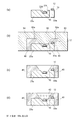
図5は、比較例にかかる発光装置であり、図5(a)は模式平面図、図5(b)はC−C線に沿った模式断面図である。本比較例において、発光素子110は第1のリード122にマウントされ、発光素子110の上部の電極(図示せず)と、第2のリード132と、がボンディングワイヤ115を用いて接続されている。また、保護素子112が第2のリード132にマウントされ、保護素子112と、第1のリード122と、がボンディングワイヤ114を用いて接続されている。
5A and 5B show a light emitting device according to a comparative example. FIG. 5A is a schematic plan view, and FIG. 5B is a schematic cross-sectional view taken along the line CC. In this comparative example, the
樹脂からなる成型体140には、光反射面となる内部側壁140bを有する凹部140aが形成されている。発光素子110及び保護素子112は、第1及び第2のリード122、132を含むリードフレームの同一の側に形成されるので、凹部140aの平面サイズは図5(a)のように大きくなり、発光素子110から内部側壁140bまでの距離が長くなり、側方に放出された光が内部側壁140bにおいて効果的に上方へ反射されない。このために光取り出し効率が低下し、高出力を得ることが困難になる。また、パッケージの平面サイズが大きくなる。
The molded
これに対して、本実施形態では、凹部40a内には発光素子10のみが配置され、保護素子12は成型体40に埋め込まれているのでパッケージの平面サイズが増大することはなく、発光素子10と光反射面との距離を短く保ち光取り出し効率を低下させることは無い。この場合、平面視で、保護素子12を内部側壁40bに重なるようにするとよい。すなわち、凹部40aの開口端の側からみて、保護素子12を内部側壁40bの下方に埋め込むようにすれば、成型体40の平面サイズを小型化でき、内部側壁40bの領域に完全に含まれるように配置すれば平面サイズの小型化がより容易となる。
On the other hand, in the present embodiment, only the
なお、リードフレームの一方の面に発光素子、他方の面に保護素子をマウントする構造とする場合、液状の導電性接着材を用いると、マウント→熱硬化工程を2回連続して行う必要があり組立時間短縮が困難であり、また薄型化が困難である。これに対して本実施形態では、保護素子12及び発光素子10はリードフレームの同一の面に設けられているので、成型体40を薄型化することが容易である。
In addition, when it is set as the structure which mounts a light emitting element on one side of a lead frame, and a protection element on the other side, when a liquid conductive adhesive is used, it is necessary to perform a mounting-> thermosetting process twice continuously. It is difficult to shorten the assembly time, and it is difficult to reduce the thickness. On the other hand, in this embodiment, since the
さらに、本実施形態において成型体40の材料を熱可塑性樹脂とすると、エポキシなどの熱硬化性からなる樹脂成型と比較して、加工がより容易でありかつ材料を繰り返し使用できるのでより経済的である。また、熱可塑性樹脂は、熱硬化性であるエポキシよりも熱膨張率が小さい。このため、熱膨張及び収縮に基づく応力を低減し、インナーリードと熱可塑性樹脂との間の接着強度が高いパッケージとでき、かつ保護素子12のチップ剥離を抑制することがより容易である。
Furthermore, if the material of the molded
図6は、本発明の第2の実施形態にかかる発光装置であり、図6(a)は模式平面図、図6(b)はA−A線に沿った模式断面図、図6(c)はB−B線に沿った模式断面図である。本実施形態において、第1のリード23は、厚いインナーリード部23aと、薄いアウターリード部23bと、を有する。また、第2のリード33は、厚いインナーリード部33aと、薄いアウターリード部33bと、を有する。インナーリード部23a、33aの厚さは、例えば0.5〜2mm、アウターリード部23b、33bの厚さは、例えば0.1〜0.5mmなどとできる。
6A and 6B show a light emitting device according to the second embodiment of the present invention. FIG. 6A is a schematic plan view, FIG. 6B is a schematic cross-sectional view along the line AA, and FIG. ) Is a schematic cross-sectional view along the line BB. In the present embodiment, the
インナーリード部23aは凹部23dを有し、発光素子10は凹部23dの底面に、接着剤11を用いてマウントされている。他方、保護素子12はインナーリード33aの上面に接着剤13を用いてマウントされている。
The
発光素子10が露出し、保護素子12と、インナーリード23a、33aと、が埋め込まれるように熱可塑性樹脂を用いて成型体40が形成されている。成型体40は凹部40aを有するが、凹部40の内部側壁40bは、インナーリード23aの内部側壁と共に光反射面である。また、インナーリード33aには発光素子10とボンディングワイヤ15を用いて接続するために成型体40に切り欠き部40dが設けられている。
The molded
本実施形態もパッケージの小型化及び薄型化、高出力化が容易である。また、発光素子10及び保護素子12のマウントにAuSnのような金属半田を用いると接着強度を高めることができ、信頼性が改善できる。さらに、図6のように、インナーリード23aにおいて、発光素子10のマウント領域の裏面側である底面23eを露出するように成型体40を形成すると、ヒートシンクなどの付設が容易となるので、動作温度を低減し信頼性改善及び高出力化が容易となる。
In this embodiment, the package can be easily reduced in size, thickness, and output. Further, when a metal solder such as AuSn is used for mounting the
図7は、第2の実施形態にかかる発光装置の製造方法を表すフローチャートであり、図8は、その工程断面図である。なお、図8に表す断面は、図6のB−B線に沿った断面図である。図8(a)のように、保護素子12をインナーリード33a上面に、AuSi(融点約370℃)またはAuSn(融点約280℃)のような共晶組成の金属半田13を用いてマウントする。マウント温度は、AuSiの場合に約400℃とし、AuSnの場合に約350℃とすると、より確実にマウントし接着強度を高めることができ、作業性も改善できる。さらに、発光素子10をインナーリード23aの凹部23dの底面にAuSnのような金属半田11を用いてマウントする(S200)。
FIG. 7 is a flowchart showing a method for manufacturing a light emitting device according to the second embodiment, and FIG. 8 is a process sectional view thereof. The cross section shown in FIG. 8 is a cross sectional view along the line BB in FIG. As shown in FIG. 8A, the
発光素子10をマウントした後に保護素子12をマウントしてもよい。いずれのマウント順序であっても、1番目のマウント工程は約400℃に昇温しAuSi半田を用い、2番目のマウント工程は約350℃に降温してAuSn半田を用いると、作業性がよく接着をより確実にできる。
The
続いて、保護素子12とインナーリード23aとをボンディングワイヤ14を用いて接続する(S202)。
Subsequently, the
発光素子10の上面が、インナーリード23aの上面よりも低くなるように凹部23dを設けると成型体40のインサート成型がより容易となる。この場合、図8(b)のように、凹部23dを覆い、インナーリード23aの上面に接触するような上金型50と、下金型(図示せず)と、の間にリードフレームを挟持し、注入口50aから熱可塑性樹脂を注入し、インサート成型を行う(S204)。インサート成型工程において、金型温度を約150℃、樹脂温度を約300℃などに設定する。
When the
フレーム温度と略同一である金型温度をAuSnなど半田材の融点よりも低くしてインサート成型ができる熱可塑性樹脂を用いると、金属半田11、13が再溶融することを抑制し、発光素子10とインナーリード23aとの間、及び保護素子12とインナーリード33aとの間において接着強度を高く保つことが容易となり、チップ剥離を抑制できる。図8(c)は金型から離型後を表す。
When a thermoplastic resin that can be insert-molded with a mold temperature that is substantially the same as the frame temperature lower than the melting point of the solder material such as AuSn, the metal solders 11 and 13 are prevented from remelting, and the
続いて、発光素子10と、インナーリード23aと、をボンディングワイヤ15を用いて接続する(S206)。
さらに、図8(d)のように成型体40の凹部40a及びインナーリード23dに液状の封止樹脂42をポッティング法などにより充填し、約200℃で熱硬化する(S208)。
Subsequently, the
Further, as shown in FIG. 8D, the
リードカット及びアウターリード23b、33bのフォーミングを行い、実装基板への実装を容易とする(S210)。 Lead cutting and forming of the outer leads 23b and 33b are performed to facilitate mounting on the mounting board (S210).
第2の実施形態にかかる発光装置の製造方法は、上記フローチャートに限定されない。例えば、接着剤11、13として導電性接着剤を用いることができ、保護素子12を成型体40に埋め込んだ後、発光素子10をマウントする工程順序とすることもできる。しかし、金属半田を用い、発光素子10及び保護素子12をマウントした後、熱可塑性樹脂を用いて成型体40を形成する製造方法を用いると、チップマウント工程を連続して行うことができるので、昇温及び降温に要する時間を短縮することが容易である。さらに、成型体40を熱硬化する必要がないので熱可塑性樹脂成型時間を短縮することができる。
The manufacturing method of the light emitting device according to the second embodiment is not limited to the above flowchart. For example, a conductive adhesive can be used as the
このようにして、本製造方法を用いると、リール・ツー・リール組立ラインでリードフレームを搬送するか、または短冊状リードフレームを搬送し、連続した組立工程の自動化が容易となる。このために、量産性に富む発光装置を提供することができる。 In this way, when this manufacturing method is used, the lead frame is transported on the reel-to-reel assembly line or the strip-shaped lead frame is transported, and automation of the continuous assembly process becomes easy. For this reason, a light-emitting device with high productivity can be provided.
以上のように、第1及び第2の実施形態にかかる発光装置によれば、ESDなどに対する保護素子12を内蔵しつつ、小型平面サイズかつ薄型の形状を有し、高光出力が可能で、機械的強度が改善された発光装置が提供される。この発光装置は、照明、車載、信号機などの用途における厳しい環境条件においても信頼性を確保することが容易である。
As described above, according to the light emitting devices according to the first and second embodiments, the
以上、図面を参照しつつ、本発明の実施の形態について説明した。しかしながら本発明はこれら実施形態に限定されない。本発明を構成する発光素子、リードフレーム、熱可塑性樹脂、封止樹脂、保護素子、接着剤、成型体の材質、形状、サイズ、配置、などに関して当業者が設計変更を行ったものであっても、本発明の主旨を逸脱しない限り本発明の範囲に包含される。 The embodiments of the present invention have been described above with reference to the drawings. However, the present invention is not limited to these embodiments. A person skilled in the art made a design change with respect to the light emitting element, lead frame, thermoplastic resin, sealing resin, protective element, adhesive, material of the molded body, shape, size, arrangement, etc. constituting the present invention. Are included in the scope of the present invention without departing from the gist of the present invention.
10 発光素子、12 保護素子、11、13 接着剤、22、23 第1のリード、32、33 第2のリード、40 成型体、40a 凹部、40b 内部側壁、Tg1、Tg2 ガラス転移温度
DESCRIPTION OF
Claims (5)
前記成型体に埋め込まれ且つその一部が前記凹部の中に露出した第1のインナーリード部を有する、第1のリードと、
前記凹部の中に露出した前記第1のインナーリード部の上面に接着された発光素子と、
前記成型体に埋め込まれ且つその一部が前記凹部の中に露出した第2のインナーリード部を有し、前記第2のインナーリード部の先端部が前記第1のインナーリード部の先端部と対向する、第2のリードと、
前記第1のインナーリード部の前記上面及び前記上面と同一の側である前記第2のインナーリード部の上面のいずれかに接着され、前記成型体に埋め込まれた保護素子と、
を備えたことを特徴とする発光装置。 A molded body made of a resin having a recess that is widened toward the opening end and whose inner side wall is a light reflecting surface;
A first lead embedded in the molded body and having a first inner lead part partially exposed in the recess;
A light emitting device bonded to the upper surface of the first inner lead exposed in the recess;
A second inner lead portion embedded in the molded body and a part of the second inner lead portion exposed in the concave portion; and a tip portion of the second inner lead portion and a tip portion of the first inner lead portion An opposing second lead;
A protective element that is bonded to any one of the upper surface of the first inner lead portion and the upper surface of the second inner lead portion that is on the same side as the upper surface, and embedded in the molded body;
A light-emitting device comprising:
前記樹脂は熱可塑性樹脂からなり、
前記第1の金属半田の融点は、前記熱可塑性樹脂のガラス転移温度よりも高いことを特徴とする請求項1または2に記載の発光装置。 The protective element is bonded using a first metal solder,
The resin is made of a thermoplastic resin,
The light emitting device according to claim 1, wherein the melting point of the first metal solder is higher than the glass transition temperature of the thermoplastic resin.
前記第1及び第2のリードを有するリードフレームの上面に前記保護素子を接着する工程と、
前記第1のインナーリード部のうちの前記発光素子の接着領域が前記凹部の中に露出し、前記保護素子と、前記第1及び第2のインナーリード部の一部と、が埋め込まれるように、前記樹脂を用いて前記成型体を形成する工程と、
を備えたことを特徴とする発光装置の製造方法。 A method for manufacturing a light emitting device according to claim 1 or 2,
Bonding the protective element to an upper surface of a lead frame having the first and second leads;
The adhesion region of the light emitting element in the first inner lead part is exposed in the recess, and the protection element and a part of the first and second inner lead parts are embedded. Forming the molded body using the resin;
A method for manufacturing a light emitting device, comprising:
前記第1及び第2のリードを有するリードフレームの上面に、前記樹脂として用いる熱可塑性樹脂のガラス転移温度よりも高い融点を有する第1の金属半田を用いて前記保護素子を接着する工程と、
前記リードフレームの前記上面に、前記ガラス転移温度よりも高い融点を有する第2の金属半田を用いて前記発光素子を接着する工程と、
前記発光素子が前記凹部の中に露出し、前記保護素子と、前記第1及び第2のインナーリード部の一部と、が埋め込まれるように、前記熱可塑性樹脂を用いて前記成型体を形成する工程と、
を備えたことを特徴とする発光装置の製造方法。
A method for manufacturing a light emitting device according to claim 1 or 2,
Adhering the protective element to the upper surface of the lead frame having the first and second leads using a first metal solder having a melting point higher than the glass transition temperature of the thermoplastic resin used as the resin;
Bonding the light emitting element to the upper surface of the lead frame using a second metal solder having a melting point higher than the glass transition temperature;
The molded body is formed using the thermoplastic resin so that the light emitting element is exposed in the recess and the protection element and a part of the first and second inner lead portions are embedded. And the process of
A method for manufacturing a light emitting device, comprising:
Priority Applications (1)
| Application Number | Priority Date | Filing Date | Title |
|---|---|---|---|
| JP2008041637A JP2009200321A (en) | 2008-02-22 | 2008-02-22 | Light-emitting device and its manufacturing method |
Applications Claiming Priority (1)
| Application Number | Priority Date | Filing Date | Title |
|---|---|---|---|
| JP2008041637A JP2009200321A (en) | 2008-02-22 | 2008-02-22 | Light-emitting device and its manufacturing method |
Publications (1)
| Publication Number | Publication Date |
|---|---|
| JP2009200321A true JP2009200321A (en) | 2009-09-03 |
Family
ID=41143494
Family Applications (1)
| Application Number | Title | Priority Date | Filing Date |
|---|---|---|---|
| JP2008041637A Pending JP2009200321A (en) | 2008-02-22 | 2008-02-22 | Light-emitting device and its manufacturing method |
Country Status (1)
| Country | Link |
|---|---|
| JP (1) | JP2009200321A (en) |
Cited By (12)
| Publication number | Priority date | Publication date | Assignee | Title |
|---|---|---|---|---|
| KR20110109222A (en) * | 2010-03-30 | 2011-10-06 | 엘지이노텍 주식회사 | Light emitting device package and fabrication method thereof |
| JP2012009530A (en) * | 2010-06-23 | 2012-01-12 | Hiroshi Ninomiya | Surface luminous body with bare chip mounted thereon and method for manufacturing the same |
| CN102751391A (en) * | 2011-04-18 | 2012-10-24 | 深圳市龙岗区横岗光台电子厂 | Light-emitting diode (LED) packaging body and manufacturing method thereof as well as LED |
| KR101649300B1 (en) * | 2015-04-13 | 2016-08-19 | 주식회사 루멘스 | Method for manufacturing light emitting device package and light emitting device package |
| KR101653926B1 (en) * | 2015-03-12 | 2016-09-02 | 조성은 | LED reflector and LED package having the same |
| KR101670951B1 (en) * | 2010-06-23 | 2016-10-31 | 서울반도체 주식회사 | Light emitting device |
| JP2017216368A (en) * | 2016-05-31 | 2017-12-07 | 日亜化学工業株式会社 | Light-emitting device |
| KR101824886B1 (en) * | 2011-03-25 | 2018-03-14 | 엘지이노텍 주식회사 | Light emitting device package |
| JP2018174355A (en) * | 2018-08-02 | 2018-11-08 | 日亜化学工業株式会社 | Light-emitting device |
| US10431572B2 (en) | 2017-05-12 | 2019-10-01 | Nichia Corporation | Light emitting device and method of manufacturing the light emitting device |
| US10756246B2 (en) | 2017-10-12 | 2020-08-25 | Nichia Corporation | Light emitting device |
| JP2021504938A (en) * | 2017-11-30 | 2021-02-15 | オスラム オーエルイーディー ゲゼルシャフト ミット ベシュレンクテル ハフツングOSRAM OLED GmbH | Manufacture of optoelectronic parts |
-
2008
- 2008-02-22 JP JP2008041637A patent/JP2009200321A/en active Pending
Cited By (16)
| Publication number | Priority date | Publication date | Assignee | Title |
|---|---|---|---|---|
| KR101693852B1 (en) * | 2010-03-30 | 2017-01-06 | 엘지이노텍 주식회사 | Light emitting device package and fabrication method thereof |
| KR20110109222A (en) * | 2010-03-30 | 2011-10-06 | 엘지이노텍 주식회사 | Light emitting device package and fabrication method thereof |
| JP2012009530A (en) * | 2010-06-23 | 2012-01-12 | Hiroshi Ninomiya | Surface luminous body with bare chip mounted thereon and method for manufacturing the same |
| KR101670951B1 (en) * | 2010-06-23 | 2016-10-31 | 서울반도체 주식회사 | Light emitting device |
| KR101824886B1 (en) * | 2011-03-25 | 2018-03-14 | 엘지이노텍 주식회사 | Light emitting device package |
| CN102751391A (en) * | 2011-04-18 | 2012-10-24 | 深圳市龙岗区横岗光台电子厂 | Light-emitting diode (LED) packaging body and manufacturing method thereof as well as LED |
| KR101653926B1 (en) * | 2015-03-12 | 2016-09-02 | 조성은 | LED reflector and LED package having the same |
| KR101649300B1 (en) * | 2015-04-13 | 2016-08-19 | 주식회사 루멘스 | Method for manufacturing light emitting device package and light emitting device package |
| JP2017216368A (en) * | 2016-05-31 | 2017-12-07 | 日亜化学工業株式会社 | Light-emitting device |
| US10431572B2 (en) | 2017-05-12 | 2019-10-01 | Nichia Corporation | Light emitting device and method of manufacturing the light emitting device |
| US11315913B2 (en) | 2017-05-12 | 2022-04-26 | Nichia Corporation | Light emitting device and method of manufacturing the light emitting device |
| US10756246B2 (en) | 2017-10-12 | 2020-08-25 | Nichia Corporation | Light emitting device |
| US11367821B2 (en) | 2017-10-12 | 2022-06-21 | Nichia Corporation | Light emitting device |
| JP2021504938A (en) * | 2017-11-30 | 2021-02-15 | オスラム オーエルイーディー ゲゼルシャフト ミット ベシュレンクテル ハフツングOSRAM OLED GmbH | Manufacture of optoelectronic parts |
| JP7152483B2 (en) | 2017-11-30 | 2022-10-12 | オスラム オーエルイーディー ゲゼルシャフト ミット ベシュレンクテル ハフツング | Manufacture of optoelectronic components |
| JP2018174355A (en) * | 2018-08-02 | 2018-11-08 | 日亜化学工業株式会社 | Light-emitting device |
Similar Documents
| Publication | Publication Date | Title |
|---|---|---|
| JP2009200321A (en) | Light-emitting device and its manufacturing method | |
| JP4013077B2 (en) | Light emitting device and manufacturing method thereof | |
| JP4359195B2 (en) | Semiconductor light emitting device, manufacturing method thereof, and semiconductor light emitting unit | |
| KR200373718Y1 (en) | High Brightness LED With Protective Function of Electrostatic Damage | |
| TWI484665B (en) | High powered light emitter packages with compact optics | |
| US7557384B2 (en) | Semiconductor light emitting device and semiconductor light emitting unit | |
| JP4826470B2 (en) | Light emitting device | |
| KR100927077B1 (en) | Optical semiconductor device and manufacturing method thereof | |
| US20060049423A1 (en) | Light-emitting device | |
| JP5819414B2 (en) | Surface mountable optoelectronic component and method for manufacturing surface mountable optoelectronic component | |
| JP2007165840A (en) | Light-emitting device | |
| TW201448290A (en) | Light emitting device and method of manufacturing the same | |
| JP2006237190A (en) | Semiconductor light emitting device | |
| JP6947995B2 (en) | Light emitting device | |
| JP6090680B2 (en) | Light emitting module | |
| JP2008108836A (en) | Semiconductor light emitting device and method for manufacturing the same | |
| KR102142715B1 (en) | Light emitting device and fabricating method | |
| JP5978631B2 (en) | Light emitting device | |
| US20070252133A1 (en) | Light emitting apparatus | |
| US9455383B2 (en) | Molded package for light emitting device and light emitting device using the same | |
| JP4797621B2 (en) | Semiconductor device and manufacturing method thereof | |
| JP4678392B2 (en) | Light emitting device and manufacturing method thereof | |
| JP5849691B2 (en) | Mounting method of light emitting element | |
| JP2007116126A (en) | Light emitting device | |
| JP2020092251A (en) | Light-emitting device and manufacturing method thereof |