JP2009199384A - Data processing apparatus - Google Patents
Data processing apparatus Download PDFInfo
- Publication number
- JP2009199384A JP2009199384A JP2008040883A JP2008040883A JP2009199384A JP 2009199384 A JP2009199384 A JP 2009199384A JP 2008040883 A JP2008040883 A JP 2008040883A JP 2008040883 A JP2008040883 A JP 2008040883A JP 2009199384 A JP2009199384 A JP 2009199384A
- Authority
- JP
- Japan
- Prior art keywords
- data
- register
- cache
- stored
- area
- Prior art date
- Legal status (The legal status is an assumption and is not a legal conclusion. Google has not performed a legal analysis and makes no representation as to the accuracy of the status listed.)
- Pending
Links
Images


Landscapes
- Executing Machine-Instructions (AREA)
Abstract
Description
本発明は、データ処理装置にかかり、特に、マイクロプロセッサに搭載されたレジスタに入出力されるデータを処理するデータ処理装置に関する。 The present invention relates to a data processing apparatus, and more particularly to a data processing apparatus that processes data input to and output from a register mounted on a microprocessor.
プロセッサは、データを保持するレジスタを備えており、当該マイクロプロセッサの実行時の性能を向上させるためには、レジスタの容量を増大することが有効である。ところが、プロセッサが複数のタスクを切り替えながら実行するマルチタスク環境下では、レジスタの状態をキャッシュメモリに記録するために要する時間が相対的に長くなる傾向にある。また、近年では、1つのCPUダイに複数のCPUコアを搭載するマルチコアプロセッサが増加している。しかしながら、このような場合には、コアを跨いだコンテキスト切り替えが発生した場合、レジスタに比べて低速なキャッシュメモリや外部メモリを経由して転送が行われるため、効率向上の阻害要因となっている。 The processor includes a register for holding data, and it is effective to increase the capacity of the register in order to improve the performance at the time of execution of the microprocessor. However, in a multitasking environment where the processor executes while switching between a plurality of tasks, the time required to record the register state in the cache memory tends to be relatively long. In recent years, there has been an increase in multi-core processors in which a plurality of CPU cores are mounted on one CPU die. However, in such a case, when context switching across cores occurs, transfer is performed via a cache memory or external memory that is slower than the register, which is an impediment to improving efficiency. .
これに対し、特許文献1では、上記アクセス時間に低減を図るべく、プロセッサにメモリよりも高速アクセス可能なメモリであるレジスタ退避用スタックを備えている。これにより、レジスタの内容の退避と復帰を高速に行っている。
On the other hand, in
一方で、タイムシェアリングシステムにおいては、特定タスクによるプロセッサ利用の独占(スタベーション)を避けるため、優先順位が高いタスクが存在している状況で、優先順位の低いタスクに対してプロセッサの割り当て時間(タイムクォンタム)を意図的に割り当てることがある(エージング)。ところが、上述したスタックメモリを用いた先入れ後出し(FILO/スタック)のコンテキスト切り替えでは、エージングを行うことができないため、選択的にコンテキスト切り替えを行うことができない。従って、結果として、処理の高速化を図ることができない、という問題があった。そして、このことは、マルチコアプロセッサにおいて、コアを跨いだコンテキスト切り替えが発生した場合には、処理の遅延が顕著である。 On the other hand, in a time-sharing system, in order to avoid the monopoly of the use of a processor by a specific task (starvation), the processor allocation time for a task with a low priority in the situation where a task with a high priority exists. (Time Quantum) may be assigned intentionally (aging). However, in the first-in last-out (FILO / stack) context switching using the stack memory described above, aging cannot be performed, and therefore context switching cannot be performed selectively. Therefore, as a result, there is a problem that the processing speed cannot be increased. This is significant in processing delay when context switching occurs across cores in a multi-core processor.
このため、本発明の目的は、上述した課題である、処理の高速化を図ることができるデータ処理装置を提供する、ことにある。 Therefore, an object of the present invention is to provide a data processing apparatus that can increase the processing speed, which is the problem described above.
そこで、本発明の一形態であるデータ処理装置は、
演算器と、当該演算器にて処理されるデータを格納するレジスタと、当該レジスタに格納されているデータの退避先となるキャッシュメモリよりもレジスタに対して高速にアクセス可能なレジスタキャッシュと、演算器がキャッシュメモリに対してアクセスしていないときにレジスタキャッシュに記憶されたデータをキャッシュメモリに記憶するメモリバスアービタと、レジスタに対するデータの入出力を制御する制御部と、を備え、
上記レジスタキャッシュは、レジスタに格納されているデータの書き出し要求に応じて当該レジスタから出力されたデータを記憶する機能を有すると共に、レジスタへのデータの復元要求に応じてレジスタキャッシュ内に記憶されたデータのうち当該復元要求されたデータを選択してレジスタに復元する機能を有する、という構成を採る。
Therefore, a data processing apparatus according to one aspect of the present invention is
An arithmetic unit, a register for storing data to be processed by the arithmetic unit, a register cache capable of accessing the register at a higher speed than a cache memory to which data stored in the register is saved, and an arithmetic operation A memory bus arbiter that stores data stored in the register cache when the device is not accessing the cache memory, and a control unit that controls input and output of data to and from the register;
The register cache has a function of storing data output from the register in response to a write request for data stored in the register, and is stored in the register cache in response to a data restoration request to the register. A configuration is adopted in which the data requested to be restored among the data is selected and restored to a register.
また、本発明の他の形態であるデータ処理方法は、
演算器と、当該演算器にて処理されるデータを格納するレジスタと、当該レジスタに格納されているデータの退避先となるキャッシュメモリよりもレジスタに対して高速にアクセス可能なレジスタキャッシュと、演算器がキャッシュメモリに対してアクセスしていないときにレジスタキャッシュに記憶されたデータをキャッシュメモリに記憶するメモリバスアービタと、レジスタに対するデータの入出力を制御する制御部と、を備えたデータ処理装置におけるデータ処理方法であって、
レジスタに格納されているデータの書き出し要求に応じて当該レジスタから出力されたデータをレジスタキャッシュに記憶し、レジスタへのデータの復元要求に応じてレジスタキャッシュ内に記憶されたデータのうち当該復元要求されたデータを選択してレジスタに復元する、
という構成を採る。
In addition, a data processing method according to another aspect of the present invention includes:
An arithmetic unit, a register for storing data to be processed by the arithmetic unit, a register cache capable of accessing the register at a higher speed than a cache memory to which data stored in the register is saved, and an arithmetic operation A data processing apparatus comprising: a memory bus arbiter that stores data stored in the register cache in the cache memory when the device is not accessing the cache memory; and a control unit that controls input / output of data to the register A data processing method in
The data output from the register is stored in the register cache in response to the data write request stored in the register, and the restoration request is stored out of the data stored in the register cache in response to the data restoration request to the register. Select the restored data and restore it to the register,
The structure is taken.
本発明は、以上のように構成されることにより、レジスタから出力されたデータを、キャッシュメモリよりも高速アクセス可能なレジスタキャッシュから所望のデータを復元させることができ、処理の高速化を図ることができる、という優れた効果を有する。 By configuring as described above, the present invention can restore desired data from a register cache that can be accessed at a higher speed than the cache memory for data output from the register, thereby speeding up the processing. It has an excellent effect of being able to.
本発明は、演算器とレジスタとを備えたマイクロプロセッサの処理をより高速にするものであり、特に、演算器及びレジスタにより構成されたコアを複数備えたマルチコアプロセッサに好適である。 The present invention increases the processing speed of a microprocessor including an arithmetic unit and a register, and is particularly suitable for a multi-core processor including a plurality of cores configured by an arithmetic unit and a register.
そして、本発明の一形態であるデータ処理装置は、
演算器と、当該演算器にて処理されるデータを格納するレジスタと、当該レジスタに格納されているデータの退避先となるキャッシュメモリよりもレジスタに対して高速にアクセス可能なレジスタキャッシュと、演算器がキャッシュメモリに対してアクセスしていないときにレジスタキャッシュに記憶されたデータをキャッシュメモリに記憶するメモリバスアービタと、レジスタに対するデータの入出力を制御する制御部と、を備え、
上記レジスタキャッシュは、レジスタに格納されているデータの書き出し要求に応じて当該レジスタから出力されたデータを記憶する機能を有すると共に、レジスタへのデータの復元要求に応じてレジスタキャッシュ内に記憶されたデータのうち当該復元要求されたデータを選択してレジスタに復元する機能を有する、
という構成を採っている。
And the data processor which is one form of the present invention,
An arithmetic unit, a register for storing data to be processed by the arithmetic unit, a register cache capable of accessing the register at a higher speed than a cache memory to which data stored in the register is saved, and an arithmetic operation A memory bus arbiter that stores data stored in the register cache when the device is not accessing the cache memory, and a control unit that controls input and output of data to and from the register;
The register cache has a function of storing data output from the register in response to a write request for data stored in the register, and is stored in the register cache in response to a data restoration request to the register. Select the data requested to be restored from the data and restore it to the register.
The structure is adopted.
上記発明によると、まず、演算器にて処理されるレジスタに格納されたデータは、メモリバスアービタを介してキャッシュメモリに退避されるか、あるいは、当該キャッシュメモリよりも高速にアクセス可能なレジスタキャッシュに記憶される。なお、レジスタキャッシュに記憶されたデータは、メモリバスアービタによって演算器がキャッシュメモリに対してアクセスしていないときに当該キャッシュメモリに記憶される。 According to the above invention, first, the data stored in the register processed by the arithmetic unit is saved in the cache memory via the memory bus arbiter, or can be accessed at a higher speed than the cache memory. Is remembered. Note that the data stored in the register cache is stored in the cache memory when the arithmetic unit is not accessing the cache memory by the memory bus arbiter.
そして、上記レジスタキャッシュは、レジスタに格納されているデータの書き出し要求があると、当該レジスタから出力されたデータを記憶する。その後、レジスタキャッシュは、レジスタへのデータの復元要求があると、当該復元要求されたデータがレジスタキャッシュ内に記憶されているか否かを検索し、該当するデータがあると、かかるデータを選択してレジスタに復元する。 When there is a write request for data stored in the register, the register cache stores the data output from the register. After that, when there is a data restoration request to the register, the register cache searches whether or not the data requested for restoration is stored in the register cache, and if there is such data, selects the data. To restore the register.
以上により、演算器は、レジスタから出力されたデータを、キャッシュメモリを介することなく、当該キャッシュメモリよりも高速アクセス可能なレジスタキャッシュから所望のデータを復元させることができる。従って、処理の高速化を図ることができる。特に、演算器とレジスタとによって構成されるコアを複数装備したマルチコアプロセッサに適用することで、コア間を跨ぐデータの移動がレジスタキャッシュを介して実行されるため、処理のさらなる高速化を実現できる。 As described above, the arithmetic unit can restore the desired data from the register cache that can be accessed at a higher speed than the cache memory without using the cache memory. Therefore, the processing speed can be increased. In particular, by applying it to a multi-core processor equipped with multiple cores composed of arithmetic units and registers, data movement across the cores is executed via a register cache, enabling further processing speedup. .
そして、具体的には、上記レジスタキャッシュは、レジスタから出力されたデータを記憶するキャッシュ領域と、当該各キャッシュ領域にそれぞれ対応するタグ領域と、を有しており、書き出し要求時に、レジスタから出力されたデータをキャッシュ領域に記憶すると共に、当該キャッシュ領域に対応するタグ領域に当該データを特定するデータ特定情報を記憶する機能と、復元要求時に、タグ領域に記憶されたデータ特定情報に基づいて当該復元要求されたデータが記憶されたキャッシュ領域を選択して、当該キャッシュ領域内のデータをレジスタに復元する機能を有する、という構成を採る。 Specifically, the register cache has a cache area for storing data output from the register and a tag area corresponding to each cache area, and is output from the register when a write request is made. Based on the function of storing the data specifying information for specifying the data in the tag area corresponding to the cache area and the data specifying information stored in the tag area at the time of the restoration request A configuration is adopted in which the cache area storing the data requested to be restored is selected and the data in the cache area is restored to the register.
また、上記レジスタキャッシュは、書き出し要求時に、指定された書き出し先アドレス情報をデータ特定情報としてタグ領域に記憶し、復元要求時に、指定された復元要求アドレス情報と一致する書き出し先アドレス情報が記憶されたタグ領域に対応するキャッシュ領域を選択して当該キャッシュ領域内のデータをレジスタに復元する、という構成を採る。 The register cache stores the specified write destination address information in the tag area as data specifying information at the time of the write request, and stores the write destination address information that matches the specified restore request address information at the time of the restore request. The cache area corresponding to the tag area is selected and the data in the cache area is restored to the register.
さらに、上記レジスタキャッシュは、書き出し要求時に、レジスタから出力されたデータを記憶したキャッシュ領域に対応するタグ領域にデータ記憶フラグを記憶し、復元要求時に、データ記憶フラグが設定されているタグ領域に記憶されたデータ特定情報に基づいて当該復元要求されたデータが記憶されたキャッシュ領域を選択する、という構成を採る。そして、上記タグ領域は、例えば、リングバッファである。 Further, the register cache stores a data storage flag in a tag area corresponding to a cache area that stores data output from the register at the time of a write request, and stores the data storage flag in a tag area in which the data storage flag is set at the time of a restoration request. A configuration is adopted in which a cache area in which the data requested to be restored is stored is selected based on the stored data specifying information. The tag area is, for example, a ring buffer.
このように、レジスタキャッシュ内に記憶するデータを、当該データを特定するデータ特定情報を格納するタグを用いて管理することで、スタックメモリ方式とは異なり、任意のデータを選択して復元することが容易となる。 In this way, the data stored in the register cache is managed using the tag for storing the data specifying information for specifying the data, so that any data can be selected and restored unlike the stack memory method. Becomes easy.
さらに、具体的には、上記レジスタキャッシュは、レジスタから出力されるデータを次に記憶するキャッシュ領域に対応するタグ領域を指定する出力先ポインタと、復元要求時に当該復元要求されたデータに対応するデータ特定情報が記憶されているか否かを検索する対象となるタグ領域を指定する検索対象ポインタと、を有し、復元要求時に、各タグ領域上を検索対象ポインタを走査させて、当該各タグ領域内に復元要求されたデータに対応するデータ特定情報が記憶されているか否かを検索する。 More specifically, the register cache corresponds to an output destination pointer that specifies a tag area corresponding to a cache area in which data output from the register is stored next, and to the data requested to be restored at the time of the restoration request. A search target pointer that designates a tag area to be searched for whether or not the data specifying information is stored, and scans the search target pointer over each tag area at the time of restoration request, It is searched whether data specifying information corresponding to the data requested to be restored is stored in the area.
そして、上記レジスタキャッシュは、復元要求時に、出力先ポインタが指定する次の前記タグ領域から検索対象ポインタを走査して、各タグ領域内に復元要求されたデータに対応するデータ特定情報が記憶されているか否かを検索する。あるいは、レジスタキャッシュは、タグ領域のうちデータ特定情報が最も早く記憶されたタグ領域を指定するデータ記憶ポインタを有しており、復元要求時に、データ記憶ポインタが指定するタグ領域から検索対象ポインタを走査して、各タグ領域内に復元要求されたデータに対応するデータ特定情報が記憶されているか否かを検索する、という構成を採る。 The register cache scans the search target pointer from the next tag area specified by the output destination pointer at the time of the restoration request, and data specifying information corresponding to the data requested to be restored is stored in each tag area. Search whether or not. Alternatively, the register cache has a data storage pointer that designates the tag area in which the data specifying information is stored earliest in the tag area, and when the restoration request is made, the search target pointer is extracted from the tag area designated by the data storage pointer. Scanning is performed to search whether or not the data specifying information corresponding to the data requested to be restored is stored in each tag area.
このとき、上記レジスタキャッシュは、出力先ポインタあるいはデータ記憶ポインタが指定するタグ領域を追い越すまで検索対象ポインタを走査して、各タグ領域内に復元要求されたデータに対応するデータ特定情報が記憶されているか否かを検索する、という構成を採る。このようにすることで、データの検索をさらに高速に実現できる。 At this time, the register cache scans the search target pointer until it passes the tag area specified by the output destination pointer or the data storage pointer, and data specifying information corresponding to the data requested to be restored is stored in each tag area. The configuration of searching for whether or not there is is adopted. By doing so, data search can be realized at higher speed.
以下、本発明の具体的な構成及び動作を、実施形態にて説明する。なお、実施形態では、本発明であるデータ処理装置が2つのコアを有するマルチコアプロセッサである場合を例示して説明するが、コアの数は2つに限定されず、それ以上であってもよく、あるいは、1つのコアのみのプロセッサに適用してもよい。また、実施形態では、レジスタに入出力されるデータの一例として、コンテキストを例示しているが、これに限定されず、いかなるデータであってもよい。 Hereinafter, specific configurations and operations of the present invention will be described in the embodiments. In the embodiment, the case where the data processing apparatus according to the present invention is a multi-core processor having two cores will be described as an example. However, the number of cores is not limited to two and may be more than that. Alternatively, it may be applied to a processor having only one core. In the embodiment, the context is illustrated as an example of data input to and output from the register. However, the present invention is not limited to this, and any data may be used.
<実施形態1>
本発明の第1の実施形態を、図1乃至図14を参照して説明する。図1は、データ処理装置の構成を示すブロック図である。図2乃至図4は、レジスタキャッシュバンクの構成を示す概略図である。図5乃至図8は、データ処理装置の動作を示すフローチャートである。図9乃至図14は、レジスタキャッシュバンクの具体的な構成及び動作を示す図である。
<
A first embodiment of the present invention will be described with reference to FIGS. FIG. 1 is a block diagram showing the configuration of the data processing apparatus. 2 to 4 are schematic diagrams showing the configuration of the register cache bank. 5 to 8 are flowcharts showing the operation of the data processing apparatus. 9 to 14 are diagrams showing a specific configuration and operation of the register cache bank.
[構成]
図1に示すように、本実施形態におけるデータ処理装置は、コアAとコアBとを備えたマルチコアプロセッサである。具体的に、データ処理装置は、発信器100と、制御回路101と、演算器102及びレジスタ103を有するCPUコアAと、演算器104及びレジスタ105を有するCPUコアBと、レジスタキャッシュバンク106と、メモリバスアービタ107と、を備えている。なお、上記発信器100は、本装置の外部に設けられていてもよい。また、本装置の外部に、メモリバスアービタ107を介してキャッシュメモリ108が接続されている。
[Constitution]
As shown in FIG. 1, the data processing apparatus according to the present embodiment is a multi-core processor including a core A and a core B. Specifically, the data processing apparatus includes a
そして、上記発信器101からの信号は、当該発信器101に設けられた出力端子1より出力され、制御回路101の入力端子2、CPUコアA,Bにそれぞれ内蔵されている各レジスタ103,105の各入力端子3,3’、レジスタキャッシュバンク106の入力端子8、メモリバスアービタ107の入力端子14、にそれぞれ供給される。これにより、上記各回路は、発信器100からのクロック信号に同期して動作する。
The signal from the
上記レジスタ103,105は、各レジスタが装備されているCPUコアA,Bの演算器102,104がそれぞれ演算を行うときに用いられるデータを保存する。
The
上記制御回路101(制御部)は、上記レジスタ103,104に対するデータの入出力を制御する。具体的には、レジスタ103,105のデータを、レジスタキャッシュバンク106またはキャッシュメモリ108のどちらに書き出すかを制御する書き出し先制御信号と、書き出し先アドレスを指定する書き出し先アドレス信号とを、出力端子5から出力する。すると、制御回路101の出力端子5より出力された書き出し先制御信号と、書き出し先アドレス信号とは、メモリバスアービタ107の入力端子13と、レジスタキャッシュバンク106の入力端子7と、にそれぞれ入力される。
The control circuit 101 (control unit) controls input / output of data to / from the
また、各レジスタ103,105に格納されているデータは、各出力端子6,6’より出力され、メモリバスアービタ107の入力端子12と、レジスタキャッシュバンク106の入力端子10と、に入力される。
Data stored in the
そして、上記レジスタキャッシュバンク106は、その入力端子7に、制御回路101からの書き出し先制御信号により、書き出し先がレジスタキャッシュバンクである旨の信号を入力されると、当該信号が入力されたタイミングで入力端子10に入力されているレジスタから出力されたデータを、レジスタキャッシュバンク106内に保存する。なお、レジスタ103,105とレジスタキャッシュバンク106とは、十分に高速なバス、つまり、キャッシュメモリ108にアクセスするよりも高速なバスで接続されている。
When the
また、レジスタキャッシュバンク106は、それ固有のアルゴリズムにより入力されたデータを管理し、レジスタ103,105からのデータが記録しきれなくなると、キャッシュメモリ108に出力していない未出力のデータをキャッシュメモリ108に出力するまで待機する。なお、上述したレジスタキャッシュバンク106の動作は、予め組み込まれた回路によって実現されたり、あるいは、プログラムが組み込まれることによって実現されてもよい。
Further, the
また、メモリバスアービタ107は、CPUコアA,Bとキャッシュメモリ108との帯域に余裕ができ次第、つまり、CPUコアA,Bがキャッシュメモリ108にアクセスしていないときに、レジスタキャッシュバンク106に記憶されている上記未出力データを、キャッシュメモリ108に出力する。
In addition, the
ここで、上記CPUコアA,Bは、現在の動作状況を保存・復元するために、全てのレジスタの内容をキャッシュメモリ108に出力する命令が実装される場合がある。この命令による処理に対して、上記レジスタキャッシュバンク106は、全てのレジスタ103,105の内容を一時的に記録する。そして、レジスタキャッシュバンク106は、記録した全てのレジスタ103,105からのデータを、制御回路101あるいはレジスタ103,105がメモリバスアービタ107にデータを出力していない間に、キャッシュメモリ108に出力する。
Here, the CPU cores A and B may be implemented with an instruction for outputting the contents of all the registers to the
また、上述したように、メモリバスアービタ107は、制御回路101あるいはレジスタ103,105からキャッシュメモリ108への入出力がある場合には、その動作を優先して実行する。一方で、それ以外の場合には、レジスタキャッシュバンク106に記憶されている未出力データを、キャッシュメモリ108に出力するよう作動する。
Further, as described above, when there is an input / output from the
このようにして、レジスタキャッシュバンク106に記憶されたレジスタ103,105から出力されたデータは、制御回路101、レジスタ103,105の動作とは独立して、キャッシュメモリ108に出力される。
In this way, the data output from the
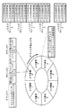
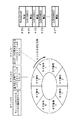
次に、上記レジスタキャッシュバンク106の構成について、図2乃至図4を参照して説明する。まず、図2に示すように、レジスタキャッシュバンク106は、レジスタから出力されたデータを保存する「レジスタキャッシュ」(0〜7)(キャッシュ領域)、各レジスタキャッシュに対応して用意され当該各レジスタキャッシュの有効/無効とキャッシュ先のアドレスを保持する「タグ」(0〜7)(タグ領域)、を有する。また、レジスタから出力されるデータを次に書き込むレジスタキャッシュに対応するタグをポイント(指定)する「カウンタ1」(出力先ポインタ)、キャッシュメモリ108またはメインメモリに書き出しが完了している最新のタグをポイントしている「カウンタ2」(書き出し完了ポインタ)、レジスタキャッシュバンク106からレジスタ103,105へ復元するデータを記憶しているレジスタキャッシュを検索するために走査するタグをポイントする「カウンタ3」(検索対象ポインタ)、を有する。ここで、上記タグは、リングバッファの形態を採っている。但し、タグは、必ずしもリングバッファ形態であることに限定されず、例えば、タグとレジスタキャッシュが関連付けられた構成であってもよく、さらには、必ずしもタグとレジスタキャッシュとを有していることにも限定されない。
Next, the configuration of the
そして、かかる構成のレジスタキャッシュバンク106は、以下のように作動するよう構成されている。ここで、上述したように、発信器100の出力端子1から出力されたクロックパルス信号に同期して、制御回路101の出力端子5からは、キャッシュメモリ108に書き出すデータの出力元を制御する信号が出力される。この出力端子5からの信号は、レジスタキャッシュバンク106の入力端子7とメモリバスアービタ107の入力端子13に入力されることで、キャッシュメモリ108に書き出されるデータの出力元が、レジスタ103,105かレジスタキャッシュバンク106かが決定される。つまり、レジスタ103,105から出力されるデータの書き出し先が、レジスタキャッシュバンク106であるか、キャッシュメモリ108であるか、を指定する書き出し要求が出力される。また、制御回路101の出力端子5から出力されているデータの書き出し先アドレス情報は、レジスタキャッシュバンク106の入力端子7とメモリバスアービタ107の入力端子13に入力され、その内容は、キャッシュメモリ108にデータを書き出す際に、書き出し先アドレス情報(データ特定情報)として利用される。
The
このように、制御回路101からレジスタキャッシュバンク106を書き出し先として指定する書き出し要求が出された場合には、レジスタキャッシュバンク106は、レジスタ103,105からのデータを所定のレジスタキャッシュに記憶すると共に、このレジスタキャッシュに対応するタグに、「書き出し先アドレス」とデータが記憶されている旨を表すフラグとなる「有効」を記憶する。このとき、具体的には、「カウンタ1」で指定されているタグに、上記「書き出し先アドレス」と「有効」を記憶し、当該タグに対応するレジスタキャッシュに、レジスタ103,105からのデータを記憶する。そして、「カウンタ1」を一つ先のタグに進める。
As described above, when a write request for designating the
また、レジスタキャッシュバンク106は、レジスタキャッシュに記憶されているデータがいっぱいになると、上述したようにメモリバスアービタ107によって、レジスタキャッシュに記憶されているデータをキャッシュメモリ108に書き出す。そして、「カウンタ2」に、書き出しが完了したレジスタキャッシュに対応するタグを指定するよう設定する。
In addition, when the data stored in the register cache is full, the
また、レジスタキャッシュバンク106は、制御回路101から、レジスタ103,105へのデータの復元要求があると、当該復元要求にかかるデータをレジスタキャッシュ106内から選択して、レジスタ103,105にロードして復元する機能を有する。具体的には、復元するデータを特定するアドレスとなる復元要求アドレスを受けると、「カウンタ3」を「カウンタ1」が指すタグの1つ先のタグを指定するよう設定し、このタグからタグ番号が増える順にタグを走査して、復元対象となるデータが格納されているレジスタキャッシュに対応するタグを検索する。なお、タグ番号7の次は、タグ番号0に戻って走査する。そして、各タグに対して、タグ内のフラグが「有効」であるか否かを調べ、「有効」であるタグ内に、復元要求アドレスと一致する書き出し先アドレスが存在するタグに対応するレジスタキャッシュに格納されたデータを選択する。そして、選択したデータを、レジスタ103,105に復元する。なお、「カウンタ3」にてタグを走査して検索する処理は、例えば、目的のデータが選択されるまで、あるいは、「カウンタ1」を指すタグを追い越すまで、順番にタグを走査して行われる。但し、上述した走査は、必ずしも上述したように「カウンタ1」の1つ先のタグから開始されることに限定されず、いかなるタグから行ってもよく、また、いかなる順番で検索を行ってもうよい。
Further, when there is a data restoration request from the
[動作]
次に、上述したデータ処理装置の動作を、図2乃至図8を参照して説明する。図2乃至図4は、レジスタキャッシュバンク106の動作を説明する図であり、図5乃至図8は、各構成の動作を示すフローチャートである。
[Operation]
Next, the operation of the above-described data processing apparatus will be described with reference to FIGS. 2 to 4 are diagrams for explaining the operation of the
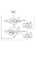
まず、図2は、レジスタキャッシュバンク106の初期状態を図示したものである。そして、上述したように、制御回路101からの書き出し要求があると、レジスタキャッシュバンク106のカウンタ1が指すタグが「無効」になっているレジスタキャッシュに(図6のステップS11でNo)、レジスタ103,105から出力されたデータを記憶する(図6のステップS12)。つまり、図2の例では、カウンタ1が指すタグ0に対応するレジスタキャッシュ0にデータを記憶し、そのタグのフラグを「有効」に更新する(図6のステップS13)。そして、その後、図3に示すように、カウンタ1を1つ先に進める(図6のステップS14)。一方、カウンタ1が指すタグのフラグが「有効」になっている場合には(図6のステップS11でYes)、レジスタキャッシュがいっぱいになっている可能性があるため、レジスタキャッシュの内容をキャッシュメモリ108に出力する(図6のステップS15)。
First, FIG. 2 illustrates the initial state of the
なお、上述したようにレジスタキャッシュバンク106からキャッシュメモリ108にデータを出力するときの動作は、例えば、図7のようになる。つまり、データがいっぱいになった場合には、カウンタ2が指すタグのフラグが「有効」であるかを調べ、「有効」であるタグに対応するレジスタキャッシュ内のデータを(図7のステップS21でYes)、キャッシュメモリ108に出力する(図7のステップS22)。そして、このレジスタキャッシュに対応するタグのフラグを「無効」に更新し(図7のステップS23)、図4に示すように、カウンタ2を1つ進める(図7のステップS24)。
As described above, the operation when data is output from the
また、上記レジスタキャッシュバンク106からキャッシュメモリ108へのデータの出力は、メモリバスアービタ107によって行われるが、このメモリバスアービタ107の動作を図5に示す。まず、上述した制御回路101からの指令により、レジスタ103,105からキャッシュメモリ108に書き出すデータがある場合には(図5のステップS1でYes)、当該レジスタ103,105からのデータをキャッシュメモリ108に出力する(図5のステップS2)。一方、レジスタ103,105からキャッシュメモリ108に書き出すデータがないときに(図5のステップS1でNo)、レジスタキャッシュバンク106からキャッシュメモリ108に出力するデータがある場合には(図5のステップS3でYes)、当該レジスタキャッシュバンク106からデータをキャッシュメモリ108に出力する(図5のステップS4)。
Data output from the
次に、制御回路101あるいはCPUコアA,Bから、データの復元要求があった場合について説明する。まず、レジスタキャッシュバンク106は、カウンタ3にカウンタ1の先のタグのデータをコピーする(図8のステップS31)。そして、カウンタ3が指すタグのフラグが「有効」であるか否かを調べ(図8のステップS32)、「有効」であるタグに対して(図8のステップS32でYes)、当該タグに記憶されている書き出し先アドレスと、復元要求にかかるデータを特定する復元要求アドレスとが一致するか否かを調べる(図8のステップS33)。このとき、一致しない場合には(図8のステップS33でNo)、カウンタ3を1つ進めて(図8のステップS34)、上述同様に、次のタグの内容を調べる。そして、アドレスが一致するタグがあると(図8のステップS33でYes)、そのタグに対応するレジスタキャッシュに記憶されているデータを、レジスタ103,105に出力して復元する(図8のステップS36)。一方、復元要求にかかるデータがレジスタキャッシュバンク106に存在しない場合には(図8のステップS32でNo)、キャッシュメモリ108あるいはメインメモリから復元要求にかかるデータを読み出して、レジスタ103,105に復元する(図8のステップS35)。
Next, a case where there is a data restoration request from the
[動作の具体例]
次に、CPUコアA,Bで実行されるコンテキストが切り替わるときの動作を、図9乃至図14を参照して説明する。
[Example of operation]
Next, the operation when the contexts executed by the CPU cores A and B are switched will be described with reference to FIGS.
まず、レジスタキャッシュバンク106の初期状態を図9に示す。この状態では、レジスタキャッシュは空であり、タグのフラグも全て「無効」となっている。
First, an initial state of the
そして、今、CPUコアAまたはCPUコアBで実行されているコンテキストがWであり、コンテキストの切り替えが発生したとする。具体的に、コンテキストがWからXに変化したとき、コンテキストXのレジスタ103,105のデータは、出力端子6または6’からレジスタキャッシュバンク106の入力端子10とメモリバスアービタ107の入力端子12に入力される。ここで、制御回路101の出力端子5から、レジスタ103,105のデータ出力先がレジスタキャッシュバンク106である旨と、書き出し先アドレスとが、レジスタキャッシュバンク106の入力端子7とメモリバスアービタ107の入力端子13に出力されていることとする。すると、レジスタ103,105のデータは、レジスタキャッシュバンク106のカウンタ1が指し示すタグに対応するレジスタキャッシュにコピーされ、タグに書き出し先アドレスを記録してタグが「有効」であるフラグをセットする。これにより、図10に示すように、タグ0には、上記レジスタ103,105から出力されたデータの書き出し先アドレスと、当該タグ0が「有効」である旨のフラグが記憶され、また、カウンタ1が次のタグであるタグ1に進む。
Now, assume that the context being executed by CPU core A or CPU core B is W, and context switching has occurred. Specifically, when the context changes from W to X, the data of the
その後、CPUコアA又はCPUコアBのコンテキストがXからさらにYに切り替わると、上述同様の処理が実行され、図11に示すように、タグ1に、「有効」のフラグと書き出し先アドレスが記憶される。そして、カウンタ1が次のタグであるタグ2に進む。さらに、CPUコアA又はCPUコアBのコンテキストがYからZに切り替わると、上述同様の処理が実行され、図12に示すように、タグ2に、「有効」のフラグと書き出し先アドレスが記憶される。そして、カウンタ1が次のタグであるタグ3に進む。このように、コンテキストが切り替わり、レジスタ103,105からデータの出力がある度に、上記動作を繰り返す。
Thereafter, when the context of the CPU core A or CPU core B is further switched from X to Y, the same processing as described above is executed, and the “valid” flag and the write destination address are stored in the
その後、CPUコアA又はCPUコアBのコンテキストがコンテキストYに切り替わり、データの復元要求があると、まず、図13に示すように、カウンタ3にカウンタ1の次のタグのデータがコピーされる。その後、カウンタ3の指し示すタグの有効・無効をチェックし、「有効」であれば、当該タグに格納されている書き出し先アドレスが復元要求されたコンテキストYの復元要求アドレスと一致するかどうかチェックする。このとき、タグ内の書き出し先アドレスが復元要求されたコンテキストYの復元要求アドレスと一致しない場合には、図14に示すように、カウンタ3を1つ進めて、再度タグの有効・無効とアドレスのチェックを行う。そして、タグが有効でアドレスが一致しているタグが見つかると、当該タグに対応するレジスタキャッシュのデータを選択して、出力端子9からレジスタ103,105の入力端子4または4’にロードする。なお、上記タグの走査は、タグとアドレスが一致するか、カウンタ3がカウンタ1を追い越すまで行われる。そして、アドレスが一致するタグが見つからなかった場合には、レジスタキャッシュバンク106上に復元要求にかかるコンテキストがキャッシュされていないものとして、キャッシュメモリ108やメインメモリからレジスタにデータをロードする。
Thereafter, when the context of CPU core A or CPU core B is switched to context Y and there is a data restoration request, first, the data of the tag next to counter 1 is copied to counter 3 as shown in FIG. Thereafter, the validity / invalidity of the tag indicated by the
以上のように、本発明によると、演算器102,104は、レジスタ103,105から出力されたデータを、キャッシュメモリ108を介することなく、当該キャッシュメモリ108よりも高速アクセス可能なレジスタキャッシュバンク106から所望のデータを復元させることができる。従って、処理の高速化を図ることができる。特に、上述したようなCPUコアを複数装備したマルチコアプロセッサに適用することで、コア間を跨ぐデータの移動が、高速アクセス可能なレジスタキャッシュバンク106を介して実行されるため、処理のさらなる高速化を実現できる。さらに、レジスタキャッシュバンク106内で、レジスタキャッシュに格納するデータをタグを用いて管理することで、スタックメモリ方式とは異なり、任意のデータを選択して復元することが容易となる。
As described above, according to the present invention, the
ここで、上述したレジスタキャッシュバンク106に、高速なメモリ、マルチポートRAM、非同期回路などを用いることで、より一層の高速化や低電力化を図ることができる。加えて、上記発信器100を外部に設置したり複数個設置したりすることでも、より一層の高速化や低電力化を図ることができる。
Here, by using a high-speed memory, a multi-port RAM, an asynchronous circuit, or the like for the above-described
また、上記では、「カウンタ3」にて「カウンタ1」の次のタグを指定して、このタグから走査を開始する場合を例示したが、これに限定されない。例えば、現在「有効」となっているタグのうち、最も早く「有効」となったタグを記憶する「カウンタ4」(データ記憶ポインタ)をレジスタキャッシュバンク106に実装し、当該「カウンタ4」に「カウンタ3」を当てて、タグの走査を開始してもよい。例えば、「カウンタ4」は、カウンタ2の一つ先のタグを指定することで、現在記憶しているもののうち、最も早く「有効」となったタグを記憶することができる。そして、この場合には、「カウンタ3」が「カウンタ4」を追い越すまで検索が実行される。
In the above description, the case where the next tag of “
本発明は、マルチコアプロセッサをはじめ、種々のプロセッサに利用することができ、産業上の利用可能性を有する。 The present invention can be used for various processors including a multi-core processor, and has industrial applicability.
100 発信器
101 制御回路
102,104 演算器
103,105 レジスタ
106 レジスタキャッシュバンク
107 メモリバスアービタ
108 キャッシュメモリ
A,B CPUコア
DESCRIPTION OF
Claims (12)
前記レジスタキャッシュは、前記レジスタに格納されているデータの書き出し要求に応じて当該レジスタから出力されたデータを記憶する機能を有すると共に、前記レジスタへのデータの復元要求に応じてレジスタキャッシュ内に記憶されたデータのうち当該復元要求されたデータを選択して前記レジスタに復元する機能を有する、
ことを特徴とするデータ処理装置。 An arithmetic unit, a register for storing data to be processed by the arithmetic unit, a register cache capable of accessing the register at a higher speed than a cache memory serving as a save destination of the data stored in the register, A memory bus arbiter that stores data stored in the register cache in the cache memory when the arithmetic unit is not accessing the cache memory; and a control unit that controls input and output of data to and from the register; With
The register cache has a function of storing data output from the register in response to a write request for data stored in the register, and is stored in the register cache in response to a data restoration request to the register. Having the function of selecting the data requested to be restored from among the received data and restoring it to the register,
A data processing apparatus.
前記書き出し要求時に、前記レジスタから出力されたデータを前記キャッシュ領域に記憶すると共に、当該キャッシュ領域に対応する前記タグ領域に当該データを特定するデータ特定情報を記憶する機能と、
前記復元要求時に、前記タグ領域に記憶された前記データ特定情報に基づいて当該復元要求されたデータが記憶された前記キャッシュ領域を選択して、当該キャッシュ領域内のデータを前記レジスタに復元する機能を有する、
ことを特徴とする請求項1記載のデータ処理装置。 The register cache has a cache area for storing data output from the register, and a tag area corresponding to each cache area,
A function of storing data output from the register in the cache area at the time of the write request, and storing data specifying information for specifying the data in the tag area corresponding to the cache area;
A function of selecting the cache area in which the data requested to be restored is stored based on the data specifying information stored in the tag area at the time of the restoration request, and restoring the data in the cache area to the register Having
The data processing apparatus according to claim 1.
ことを特徴とする請求項2記載のデータ処理装置。 The register cache stores the specified write destination address information in the tag area as the data specifying information at the time of the write request, and the write destination address information that matches the specified restore request address information at the time of the restore request Selecting the cache area corresponding to the tag area in which is stored, and restoring the data in the cache area to the register,
The data processing apparatus according to claim 2.
ことを特徴とする請求項2又は3記載のデータ処理装置。 The register cache stores a data storage flag in the tag area corresponding to the cache area storing the data output from the register at the time of the write request, and the data storage flag is set at the time of the restoration request. Selecting the cache area in which the data requested to be restored is stored based on the data specifying information stored in the tag area.
The data processing apparatus according to claim 2 or 3, wherein
ことを特徴とする請求項2,3又は4記載のデータ処理装置。 The tag area is a ring buffer.
5. A data processing apparatus according to claim 2, 3 or 4.
前記復元要求時に、前記各タグ領域上を前記検索対象ポインタを走査させて、当該各タグ領域内に復元要求されたデータに対応する前記データ特定情報が記憶されているか否かを検索する、
ことを特徴とする請求項2,3,4又は5記載のデータ処理装置。 The register cache includes an output destination pointer that specifies the tag area corresponding to the cache area in which data output from the register is stored next, and the data specification corresponding to the data requested to be restored at the time of the restoration request A search target pointer for designating the tag area to be searched for whether or not information is stored, and
At the time of the restoration request, the search target pointer is scanned on each tag area to search whether or not the data specifying information corresponding to the data requested to be restored is stored in each tag area.
6. A data processing apparatus according to claim 2, 3, 4 or 5.
ことを特徴とする請求項6記載のデータ処理装置。 The register cache scans the search target pointer from the next tag area specified by the output destination pointer at the time of the restoration request, and the data specifying information corresponding to the data requested to be restored in each tag area Search whether or not is stored,
The data processing apparatus according to claim 6.
ことを特徴とする請求項6記載のデータ処理装置。 The register cache has a data storage pointer that specifies the tag area in which the data specifying information is stored earliest in the tag area, and the tag area specified by the data storage pointer at the time of the restoration request The search target pointer is scanned from to search whether or not the data specifying information corresponding to the data requested to be restored is stored in each tag area.
The data processing apparatus according to claim 6.
ことを特徴とする請求項7又は8記載のデータ処理装置。 The register cache scans the search target pointer until it passes the tag area specified by the output destination pointer or the data storage pointer, and the data specifying information corresponding to the data requested to be restored in each tag area Search whether or not is stored,
9. The data processing apparatus according to claim 7, wherein the data processing apparatus is a data processing apparatus.
ことを請求項1,2,3,4,5,6,7,8又は9記載のデータ処理装置。 Provided with a plurality of cores constituted by the arithmetic unit and the register,
10. A data processing apparatus according to claim 1, 2, 3, 4, 5, 6, 7, 8 or 9.
前記レジスタに格納されているデータの書き出し要求に応じて当該レジスタから出力されたデータを前記レジスタキャッシュに記憶し、前記レジスタへのデータの復元要求に応じてレジスタキャッシュ内に記憶されたデータのうち当該復元要求されたデータを選択して前記レジスタに復元する、
ことを特徴とするデータ処理方法。 An arithmetic unit, a register for storing data to be processed by the arithmetic unit, a register cache capable of accessing the register at a higher speed than a cache memory serving as a save destination of the data stored in the register, A memory bus arbiter that stores data stored in the register cache in the cache memory when the arithmetic unit is not accessing the cache memory; and a control unit that controls input and output of data to and from the register; A data processing method in a data processing apparatus comprising:
The data output from the register is stored in the register cache in response to the data write request stored in the register, and the data stored in the register cache in response to the data restoration request to the register Select the data requested to be restored and restore it to the register;
A data processing method.
前記復元要求時に、前記タグ領域に記憶された前記データ特定情報に基づいて当該復元要求されたデータが記憶された前記キャッシュ領域を選択して、当該キャッシュ領域内のデータを前記レジスタに復元する、
ことを特徴とする請求項11記載のデータ処理方法。
At the time of the write request, the data output from the register is stored in a cache area provided in the register cache, and the data is stored in the tag area provided in the register cache corresponding to the cache area. Stores data identification information to be identified,
At the time of the restoration request, the cache area in which the data requested to be restored is stored based on the data specifying information stored in the tag area is selected, and the data in the cache area is restored to the register.
The data processing method according to claim 11.
Priority Applications (1)
| Application Number | Priority Date | Filing Date | Title |
|---|---|---|---|
| JP2008040883A JP2009199384A (en) | 2008-02-22 | 2008-02-22 | Data processing apparatus |
Applications Claiming Priority (1)
| Application Number | Priority Date | Filing Date | Title |
|---|---|---|---|
| JP2008040883A JP2009199384A (en) | 2008-02-22 | 2008-02-22 | Data processing apparatus |
Publications (1)
| Publication Number | Publication Date |
|---|---|
| JP2009199384A true JP2009199384A (en) | 2009-09-03 |
Family
ID=41142803
Family Applications (1)
| Application Number | Title | Priority Date | Filing Date |
|---|---|---|---|
| JP2008040883A Pending JP2009199384A (en) | 2008-02-22 | 2008-02-22 | Data processing apparatus |
Country Status (1)
| Country | Link |
|---|---|
| JP (1) | JP2009199384A (en) |
Cited By (3)
| Publication number | Priority date | Publication date | Assignee | Title |
|---|---|---|---|---|
| JP2013516006A (en) * | 2009-12-29 | 2013-05-09 | エンパイア テクノロジー ディベロップメント エルエルシー | Shared memory for energy efficient multi-core processors |
| JP2013532331A (en) * | 2010-06-29 | 2013-08-15 | インテル・コーポレーション | Apparatus, method and system for improving power performance efficiency by combining first core type and second core type |
| CN105677580A (en) * | 2015-12-30 | 2016-06-15 | 杭州华为数字技术有限公司 | Method and device for accessing cache |
Citations (8)
| Publication number | Priority date | Publication date | Assignee | Title |
|---|---|---|---|---|
| JPH08320825A (en) * | 1995-05-25 | 1996-12-03 | Hitachi Ltd | Data processor |
| JP2001209577A (en) * | 1999-11-16 | 2001-08-03 | Matsushita Electric Ind Co Ltd | Information recording and reproducing device |
| JP2003330797A (en) * | 2002-05-16 | 2003-11-21 | Sony Corp | Storage device, recording and/or reproduction device, information storage system, storage method, program and recording medium |
| JP2005129168A (en) * | 2003-10-24 | 2005-05-19 | Ricoh Co Ltd | Device and method for recording information, and program |
| JP2005284646A (en) * | 2004-03-29 | 2005-10-13 | Toshiba Corp | Microprocessor |
| JP2006099335A (en) * | 2004-09-29 | 2006-04-13 | Seiko Epson Corp | Context processor |
| JP2006139495A (en) * | 2004-11-11 | 2006-06-01 | Seiko Epson Corp | Arithmetic processing unit |
| JP2007213486A (en) * | 2006-02-13 | 2007-08-23 | Fujitsu Ltd | Timer management device and timer management method |
-
2008
- 2008-02-22 JP JP2008040883A patent/JP2009199384A/en active Pending
Patent Citations (8)
| Publication number | Priority date | Publication date | Assignee | Title |
|---|---|---|---|---|
| JPH08320825A (en) * | 1995-05-25 | 1996-12-03 | Hitachi Ltd | Data processor |
| JP2001209577A (en) * | 1999-11-16 | 2001-08-03 | Matsushita Electric Ind Co Ltd | Information recording and reproducing device |
| JP2003330797A (en) * | 2002-05-16 | 2003-11-21 | Sony Corp | Storage device, recording and/or reproduction device, information storage system, storage method, program and recording medium |
| JP2005129168A (en) * | 2003-10-24 | 2005-05-19 | Ricoh Co Ltd | Device and method for recording information, and program |
| JP2005284646A (en) * | 2004-03-29 | 2005-10-13 | Toshiba Corp | Microprocessor |
| JP2006099335A (en) * | 2004-09-29 | 2006-04-13 | Seiko Epson Corp | Context processor |
| JP2006139495A (en) * | 2004-11-11 | 2006-06-01 | Seiko Epson Corp | Arithmetic processing unit |
| JP2007213486A (en) * | 2006-02-13 | 2007-08-23 | Fujitsu Ltd | Timer management device and timer management method |
Cited By (5)
| Publication number | Priority date | Publication date | Assignee | Title |
|---|---|---|---|---|
| JP2013516006A (en) * | 2009-12-29 | 2013-05-09 | エンパイア テクノロジー ディベロップメント エルエルシー | Shared memory for energy efficient multi-core processors |
| US9367462B2 (en) | 2009-12-29 | 2016-06-14 | Empire Technology Development Llc | Shared memories for energy efficient multi-core processors |
| JP2013532331A (en) * | 2010-06-29 | 2013-08-15 | インテル・コーポレーション | Apparatus, method and system for improving power performance efficiency by combining first core type and second core type |
| CN105677580A (en) * | 2015-12-30 | 2016-06-15 | 杭州华为数字技术有限公司 | Method and device for accessing cache |
| CN105677580B (en) * | 2015-12-30 | 2019-04-12 | 杭州华为数字技术有限公司 | The method and apparatus of access cache |
Similar Documents
| Publication | Publication Date | Title |
|---|---|---|
| US10860326B2 (en) | Multi-threaded instruction buffer design | |
| US7953953B2 (en) | Method and apparatus for reducing page replacement time in system using demand paging technique | |
| KR100278328B1 (en) | Cache miss buffer | |
| US8683093B2 (en) | Memory system having high data transfer efficiency and host controller | |
| US9043806B2 (en) | Information processing device and task switching method | |
| KR100955433B1 (en) | Cache memory having pipeline structure and method for controlling the same | |
| EP0019358B1 (en) | Hierarchical data storage system | |
| JP2002287959A (en) | Load store queue | |
| US7913059B2 (en) | Information processing device, data transfer method, and information storage medium | |
| US10191846B2 (en) | Cache memory for particular data | |
| JP2009199384A (en) | Data processing apparatus | |
| JP2010061620A (en) | Dma device and dma transfer method | |
| EP3588319B1 (en) | Memory module | |
| KR102076248B1 (en) | Selective Delay Garbage Collection Method And Memory System Using The Same | |
| JP2004326175A (en) | Processor, cache system, and cache memory | |
| CN102385555A (en) | Caching system and method of data caching | |
| JP2007286990A (en) | Cache memory device, cache memory control method to be used for the same and program therefor | |
| JP2001022581A (en) | Data processor and computer readable storage medium | |
| US20080195805A1 (en) | Micro Controller Unit System Including Flash Memory and Method of Accessing the Flash Memory By the Micro Controller Unit | |
| JPH04266140A (en) | Address conversion buffer device | |
| JP2010205088A (en) | Vector processing apparatus and vector processing method | |
| JP2000066946A (en) | Memory controller | |
| JP2003330795A (en) | Cache memory control device | |
| JPH08123722A (en) | Method and device for controlling storage in information processing system | |
| JPH02178838A (en) | Data processor |
Legal Events
| Date | Code | Title | Description |
|---|---|---|---|
| RD03 | Notification of appointment of power of attorney |
Free format text: JAPANESE INTERMEDIATE CODE: A7423 Effective date: 20100618 |
|
| A977 | Report on retrieval |
Free format text: JAPANESE INTERMEDIATE CODE: A971007 Effective date: 20100809 |
|
| A131 | Notification of reasons for refusal |
Free format text: JAPANESE INTERMEDIATE CODE: A131 Effective date: 20100817 |
|
| A02 | Decision of refusal |
Free format text: JAPANESE INTERMEDIATE CODE: A02 Effective date: 20101214 |