JP2009193631A - Nonvolatile semiconductor memory device - Google Patents
Nonvolatile semiconductor memory device Download PDFInfo
- Publication number
- JP2009193631A JP2009193631A JP2008032820A JP2008032820A JP2009193631A JP 2009193631 A JP2009193631 A JP 2009193631A JP 2008032820 A JP2008032820 A JP 2008032820A JP 2008032820 A JP2008032820 A JP 2008032820A JP 2009193631 A JP2009193631 A JP 2009193631A
- Authority
- JP
- Japan
- Prior art keywords
- word line
- pass voltage
- line
- read pass
- selected word
- Prior art date
- Legal status (The legal status is an assumption and is not a legal conclusion. Google has not performed a legal analysis and makes no representation as to the accuracy of the status listed.)
- Pending
Links
- 239000004065 semiconductor Substances 0.000 title claims abstract description 14
- 238000009826 distribution Methods 0.000 description 20
- 230000008878 coupling Effects 0.000 description 8
- 238000010168 coupling process Methods 0.000 description 8
- 238000005859 coupling reaction Methods 0.000 description 8
- 238000000034 method Methods 0.000 description 6
- 238000010586 diagram Methods 0.000 description 5
- 239000003990 capacitor Substances 0.000 description 4
- 230000000694 effects Effects 0.000 description 3
- 238000013500 data storage Methods 0.000 description 1
Images


Classifications
-
- G—PHYSICS
- G11—INFORMATION STORAGE
- G11C—STATIC STORES
- G11C16/00—Erasable programmable read-only memories
- G11C16/02—Erasable programmable read-only memories electrically programmable
- G11C16/04—Erasable programmable read-only memories electrically programmable using variable threshold transistors, e.g. FAMOS
- G11C16/0483—Erasable programmable read-only memories electrically programmable using variable threshold transistors, e.g. FAMOS comprising cells having several storage transistors connected in series
-
- G—PHYSICS
- G11—INFORMATION STORAGE
- G11C—STATIC STORES
- G11C16/00—Erasable programmable read-only memories
- G11C16/02—Erasable programmable read-only memories electrically programmable
- G11C16/06—Auxiliary circuits, e.g. for writing into memory
- G11C16/26—Sensing or reading circuits; Data output circuits
-
- G—PHYSICS
- G11—INFORMATION STORAGE
- G11C—STATIC STORES
- G11C16/00—Erasable programmable read-only memories
- G11C16/02—Erasable programmable read-only memories electrically programmable
- G11C16/06—Auxiliary circuits, e.g. for writing into memory
- G11C16/34—Determination of programming status, e.g. threshold voltage, overprogramming or underprogramming, retention
- G11C16/3436—Arrangements for verifying correct programming or erasure
- G11C16/3454—Arrangements for verifying correct programming or for detecting overprogrammed cells
Landscapes
- Engineering & Computer Science (AREA)
- Microelectronics & Electronic Packaging (AREA)
- Read Only Memory (AREA)
Abstract
Description
この発明は、電気的書き換え可能な不揮発性半導体記憶装置(EEPROM)に係り、特にメモリセルを複数個直列接続してNANDストリングを構成するNAND型フラッシュメモリのデータ読み出し手法に関する。 The present invention relates to an electrically rewritable nonvolatile semiconductor memory device (EEPROM), and more particularly to a data read method of a NAND flash memory in which a plurality of memory cells are connected in series to form a NAND string.
NAND型フラッシュメモリは、大容量化が容易なEEPROMの一つとして知られている。NAND型フラッシュメモリのデータ読み出し動作では、NANDストリング内の非選択セルをパストランジスタとして動作させて、選択セルのオンオフ状態を検出する。即ち、選択セルには、そのしきい値分布を判定するに必要な読み出し電圧を与え、残りの非選択セルには、セルデータによらずオンする読み出しパス電圧を与えて、プリチャージしたビット線が放電されるか否かによりデータを判定する。 The NAND flash memory is known as one of EEPROMs that can be easily increased in capacity. In the data read operation of the NAND flash memory, the non-selected cell in the NAND string is operated as a pass transistor to detect the on / off state of the selected cell. That is, a read voltage necessary for determining the threshold distribution is applied to the selected cell, and a read pass voltage that is turned on regardless of the cell data is applied to the remaining non-selected cells, so that the precharged bit line The data is determined by whether or not the battery is discharged.
しかし、NAND型フラッシュメモリの微細化が進む中、データの読み出し時の信頼性が問題になっている。特に隣接セル間の容量結合が読み出し動作に影響を与える。例えば、選択セルに隣接する非選択セルが、フローティングゲート電位が十分に高くならず、従ってパストランジスタとして十分なセル電流を流せない、という事態が生じる。特に選択セルのセル電流下流側(ソース線コンタクト側)の非選択セルのチャネル抵抗は、負帰還効果によりセル電流を引き下げる方向に働くから、問題である。この読み出し時のセル電流の低下は、誤読み出しの原因やセンス時間の増大をもたらす。 However, with the progress of miniaturization of the NAND flash memory, reliability at the time of data reading has become a problem. In particular, capacitive coupling between adjacent cells affects the read operation. For example, a situation occurs in which a non-selected cell adjacent to a selected cell does not have a sufficiently high floating gate potential, and therefore a sufficient cell current cannot be passed as a pass transistor. In particular, the channel resistance of a non-selected cell on the cell current downstream side (source line contact side) of the selected cell is a problem because it works in a direction to lower the cell current due to the negative feedback effect. This decrease in cell current at the time of reading brings about a cause of erroneous reading and an increase in sensing time.
NAND型フラッシュメモリにおいて、微細化によるセル間容量結合の読み出し動作への影響を考慮した提案は、既にいくつかなされている。例えば、特許文献1には、書き込みベリファイの読み出し時、選択ワード線に隣接する非選択ワード線に対して、残りの非選択ワード線より低い読み出しパス電圧を与える例が開示されている。
この発明は、データ読み出しの信頼性向上を図った不揮発性半導体記憶装置を提供することを目的とする。 SUMMARY OF THE INVENTION An object of the present invention is to provide a nonvolatile semiconductor memory device that improves the reliability of data reading.
この発明の一態様による不揮発性半導体記憶装置は、
複数個直列接続された電気的書き換え可能な不揮発性メモリセルとその両端をそれぞれビット線及びソース線に接続するための第1及び第2の選択ゲートトランジスタとを有するNANDストリングと、
前記複数のメモリセルの制御ゲートがそれぞれ接続された複数のワード線と、
前記第1及び第2の選択ゲートトランジスタのゲートがそれぞれ接続された第1及び第2の選択ゲート線とを備え、
選択ワード線に読み出し電圧が与えられるデータ読み出し時、前記選択ワード線の前記第1の選択ゲート線側にある非選択ワード線のうち前記選択ワード線に隣接するものに第1の読み出しパス電圧が、その他の非選択ワード線に第1の読み出しパス電圧より低い第2の読み出しパス電圧が与えられ、前記選択ワード線の前記第2の選択ゲート線側にある非選択ワード線に前記第1の読み出しパス電圧より高い第3の読み出しパス電圧が与えられる。
A nonvolatile semiconductor memory device according to one aspect of the present invention is provided.
A NAND string having a plurality of electrically rewritable nonvolatile memory cells connected in series and first and second select gate transistors for connecting both ends of the nonvolatile memory cells to a bit line and a source line, respectively;
A plurality of word lines to which control gates of the plurality of memory cells are respectively connected;
First and second select gate lines to which the gates of the first and second select gate transistors are respectively connected;
At the time of data reading in which a read voltage is applied to a selected word line, a first read pass voltage is applied to an unselected word line adjacent to the selected word line on the first selected gate line side of the selected word line. A second read pass voltage lower than the first read pass voltage is applied to the other non-selected word lines, and the first non-selected word line on the second select gate line side of the selected word line is supplied with the first read pass voltage. A third read pass voltage higher than the read pass voltage is provided.
この発明の他の態様による不揮発性半導体記憶装置は、
複数個直列接続された電気的書き換え可能な不揮発性メモリセルとその両端をそれぞれビット線及びソース線に接続するための第1及び第2の選択ゲートトランジスタとを有するNANDストリングと、
前記複数のメモリセルの制御ゲートがそれぞれ接続された複数のワード線と、
前記第1及び第2の選択ゲートトランジスタのゲートがそれぞれ接続された第1及び第2の選択ゲート線とを備え、
選択ワード線に読み出し電圧が与えられるデータ読み出し時、前記選択ワード線の前記第1の選択ゲート線側にある非選択ワード線のうち前記選択ワード線に隣接するものに第1の読み出しパス電圧が、その他の非選択ワード線に第1の読み出しパス電圧より低い第2の読み出しパス電圧が与えられ、前記選択ワード線の前記第2の選択ゲート線側にある非選択ワード線に前記第1の読み出しパス電圧が与えられる。
A non-volatile semiconductor memory device according to another aspect of the present invention includes:
A NAND string having a plurality of electrically rewritable nonvolatile memory cells connected in series and first and second select gate transistors for connecting both ends of the nonvolatile memory cells to a bit line and a source line, respectively;
A plurality of word lines to which control gates of the plurality of memory cells are respectively connected;
First and second select gate lines to which the gates of the first and second select gate transistors are respectively connected;
At the time of data reading in which a read voltage is applied to a selected word line, a first read pass voltage is applied to an unselected word line adjacent to the selected word line on the first selected gate line side of the selected word line. A second read pass voltage lower than the first read pass voltage is applied to the other non-selected word lines, and the first non-selected word line on the second select gate line side of the selected word line is supplied with the first read pass voltage. A read pass voltage is provided.
この発明の更に他の態様による不揮発性半導体記憶装置は、
複数個直列接続された電気的書き換え可能な不揮発性メモリセルとその両端をそれぞれビット線及びソース線に接続するための第1及び第2の選択ゲートトランジスタとを有するNANDストリングと、
前記複数のメモリセルの制御ゲートがそれぞれ接続された複数のワード線と、
前記第1及び第2の選択ゲートトランジスタのゲートがそれぞれ接続された第1及び第2の選択ゲート線とを備え、
選択ワード線に読み出し電圧が与えられるデータ読み出し時、前記選択ワード線の前記第1の選択ゲート線側にある非選択ワード線のうち前記選択ワード線に隣接するものに第1の読み出しパス電圧が、その他の非選択ワード線に第1の読み出しパス電圧より低い第2の読み出しパス電圧が与えられ、前記選択ワード線の前記第2の選択ゲート線側にある非選択ワード線のうち前記選択ワード線に隣接するものに前記第1の読み出しパス電圧より高い第3の読み出しパス電圧が、その他の非選択ワード線に前記第1の読み出しパス電圧が与えられる。
A non-volatile semiconductor memory device according to still another aspect of the present invention provides:
A NAND string having a plurality of electrically rewritable nonvolatile memory cells connected in series and first and second select gate transistors for connecting both ends of the nonvolatile memory cells to a bit line and a source line, respectively;
A plurality of word lines to which control gates of the plurality of memory cells are respectively connected;
First and second select gate lines to which the gates of the first and second select gate transistors are respectively connected;
At the time of data reading in which a read voltage is applied to a selected word line, a first read pass voltage is applied to an unselected word line adjacent to the selected word line on the first selected gate line side of the selected word line. A second read pass voltage lower than the first read pass voltage is applied to the other non-selected word lines, and the selected word among the non-selected word lines on the second selection gate line side of the selected word line A third read pass voltage higher than the first read pass voltage is applied to the line adjacent to the line, and the first read pass voltage is applied to the other unselected word lines.
この発明によれば、データ読み出しの信頼性向上を図った不揮発性半導体記憶装置を提供することができる。 According to the present invention, it is possible to provide a nonvolatile semiconductor memory device in which the reliability of data reading is improved.
以下、図面を参照して、この発明の実施の形態を説明する。 Embodiments of the present invention will be described below with reference to the drawings.
図8は、一実施の形態によるNAND型フラッシュメモリのメモリコア部の等価回路を示している。メモリセルアレイ1は、複数のメモリセルが直列接続されたNANDストリング(NANDセルユニット)5を配列して構成されている。この例では、NANDストリング5は、32個のメモリセルM0−M31が直列接続され、その一端が選択ゲートトランジスタSG1を介してビット線BLに、他端が選択ゲートトランジスタSG2を介して共通ソース線CELSRCに接続されている。
FIG. 8 shows an equivalent circuit of the memory core part of the NAND flash memory according to the embodiment. The
メモリセルM0−M31の制御ゲートは、それぞれワード線WL0−WL31に接続され、選択ゲートトランジスタSG1,SG2のゲートはそれぞれ選択ゲート線SGD,SGSに接続されている。 The control gates of the memory cells M0 to M31 are connected to the word lines WL0 to WL31, respectively, and the gates of the selection gate transistors SG1 and SG2 are connected to the selection gate lines SGD and SGS, respectively.
ワード線WL0−WL31及び選択ゲート線SGS,SGDを選択駆動するのが、ロウデコーダ2である。ビット線BLは、ページバッフア3を構成する各センスアンプS/Aに接続される。ワード線を共有する複数のNANDストリングの集合は、消去の単位となるブロック4を構成し、ビット線BLの方向に複数ブロックが配列される。
The
図9は、通常のNAND型フラッシュメモリで行われている読み出し動作の電圧波形である。図10のようなしきい値分布の2値データ読み出しの場合であれば、選択ワード線に読み出し電圧Vcg(例えば0.4V)を、非選択ワード線には、読み出しパス電圧Vread(例えば5V)を、ビット線側の選択ゲート線SGDには選択ゲートトランジスタをオンさせる電圧Vsg(例えば4V)をそれぞれ与えた状態で、ビット線プリチャージを行い(タイミングT0)、所定のビット線電圧VBL(例えば1V)まで充電する。 FIG. 9 is a voltage waveform of a read operation performed in a normal NAND flash memory. In the case of binary data reading with a threshold distribution as shown in FIG. 10, a read voltage Vcg (eg, 0.4 V) is applied to the selected word line, and a read pass voltage Vread (eg, 5 V) is applied to the non-selected word line. A bit line precharge is performed (timing T0) in a state where a voltage Vsg (for example, 4V) for turning on the selection gate transistor is applied to the selection gate line SGD on the bit line side, and a predetermined bit line voltage VBL (for example, 1V) ).
図10に示すように、読み出し電圧Vcgは、データ“0”,“1”のしきい値分布の間に、即ち、データ“1”セル(消去セル)ではセル電流が流れ、データ“0”セル(書き込みセル)ではセル電流が流れないように設定される。読み出しパス電圧Vreadは、データ“0”,“1”に拘わらずセルをオンさせるに十分な電圧である。 As shown in FIG. 10, the read voltage Vcg is between the threshold distributions of the data “0” and “1”, that is, the cell current flows in the data “1” cell (erase cell), and the data “0”. The cell (write cell) is set so that no cell current flows. The read pass voltage Vread is a voltage sufficient to turn on the cell regardless of the data “0” and “1”.
ビット線プリチャージの後、ソース線側の選択ゲート線SGSに選択ゲートトランジスタをオンさせる電圧Vsgを与える(タイミングT1)。これにより、選択セルがデータ“1”であれば、NANDストリングは導通してビット線BLが放電され、データ“0”であれば、NANDストリングは導通せず、ビット線が放電されない。このビット線の放電の有無(または大小)を検出することにより、データを判別することができる。 After the bit line precharge, a voltage Vsg for turning on the selection gate transistor is applied to the selection gate line SGS on the source line side (timing T1). Thus, if the selected cell is data “1”, the NAND string is conductive and the bit line BL is discharged, and if data is “0”, the NAND string is not conductive and the bit line is not discharged. Data can be determined by detecting the presence or absence (or magnitude) of this bit line discharge.
このような通常の読み出し動作での問題を、具体的に説明する。微細化が進むに従い、ワード線間距離が近くなってくるが、ゲート絶縁膜の膜厚を薄くすることはセル特性の信頼性上制限がある。その結果、隣接セルのワード線間あるいはワード線とフローティングゲート間の容量結合が大きくなる。 A problem in such a normal read operation will be specifically described. As the miniaturization progresses, the distance between the word lines becomes shorter. However, reducing the thickness of the gate insulating film has a limitation on the reliability of the cell characteristics. As a result, the capacitive coupling between the word lines of adjacent cells or between the word line and the floating gate is increased.
図11は、NANDセルストリング内の隣接セル間の容量結合の様子を示している。フローティングゲート(FG)は、その上のワード線即ちコントロールゲート(CG)及びセルチャネルと容量C1及びC2で結合する他、隣接セルのフローティングゲート及びコントロールゲートとの間でそれぞれ容量C3及びC4で結合する。そして容量C3,C4が容量C1,C2に対して無視できない大きさになると、隣接セル間の容量結合が読み出し動作に影響を与える。 FIG. 11 shows a state of capacitive coupling between adjacent cells in the NAND cell string. The floating gate (FG) is coupled to the word line, that is, the control gate (CG) and the cell channel thereon by the capacitors C1 and C2, and is coupled to the floating gate and the control gate of adjacent cells by the capacitors C3 and C4, respectively. To do. When the capacitors C3 and C4 have a size that cannot be ignored with respect to the capacitors C1 and C2, capacitive coupling between adjacent cells affects the read operation.
図12は、非選択ワード線に一律に読み出しパス電圧Vreadを与えた場合のNANDストリング内のワード線WL(コントロールゲートCG)及びフローティングゲートFGの電圧分布を示している。 FIG. 12 shows the voltage distribution of the word line WL (control gate CG) and the floating gate FG in the NAND string when the read pass voltage Vread is uniformly applied to the unselected word lines.
フローティングゲートFGの電圧は、本来は直上のコントロールゲートCGとセルチャネルとの容量分割により決まり、非選択セルのフローティングゲートFGは、Vread’(<Vread)になる。しかし、非選択セルのうち選択セルに隣接するセルでは、図12に示すように、選択セルからの容量結合で、フローティングゲートFGの電圧は実質的に低くなる。逆に、選択セルのフローティングゲートの電圧は、隣接する非選択セルの影響で高くなる。従って、非選択セルが十分にオンせず、また選択セルもデータ“1”であっても十分にオンしない、という事態が生じる。 The voltage of the floating gate FG is originally determined by capacitive division between the control gate CG and the cell channel directly above, and the floating gate FG of the non-selected cell becomes Vread ′ (<Vread). However, in the non-selected cells adjacent to the selected cell, as shown in FIG. 12, the voltage of the floating gate FG is substantially lowered due to capacitive coupling from the selected cell. On the contrary, the voltage of the floating gate of the selected cell becomes higher due to the influence of the adjacent non-selected cell. Therefore, a situation occurs in which the unselected cell is not sufficiently turned on, and the selected cell is not sufficiently turned on even if the data is “1”.
この実施の形態では、非選択ワード線に与える読み出しパス電圧の最適化により、データ読み出しの信頼性向上を図る。以下、具体的に説明する。 In this embodiment, data read reliability is improved by optimizing the read pass voltage applied to the unselected word lines. This will be specifically described below.
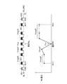
[実施態様1]
図1は、実施態様1によるデータ読み出し時のNANDセストリング内の電圧分布を示している。選択ワード線には、セルデータのしきい値分布の間に設定された読み出し電圧Vcgを、選択ワード線のビット線(BL)コンタクト側(選択ゲート線SGD側)にある非選択ワード線については、選択ワード線に隣接するものに読み出しパス電圧Vread1を、それ以外の非選択ワード線にVread1より低い読み出しパス電圧Vread2を与える。選択ワード線のソース線(CELSRC)コンタクト側(選択ゲート線SGS側)にある非選択ワード線については、Vread1より高い読み出しパス電圧Vread3を与える。
[Embodiment 1]
FIG. 1 shows a voltage distribution in the NAND cestell at the time of data reading according to the first embodiment. For the selected word line, the read voltage Vcg set during the threshold distribution of the cell data is applied to the unselected word line on the bit line (BL) contact side (selected gate line SGD side) of the selected word line. The read pass voltage Vread1 is applied to the one adjacent to the selected word line, and the read pass voltage Vread2 lower than Vread1 is applied to the other non-selected word lines. A read pass voltage Vread3 higher than Vread1 is applied to the unselected word line on the source line (CELSRC) contact side (selected gate line SGS side) of the selected word line.
これは、読み出しパス電圧Vread2を、図12で説明した通常用いられている一律の読み出しパス電圧Vreadであるとして、これより高い読み出しパス電圧Vread1を選択ゲート線SGD側の隣接選択ワード線に、また更にそれより高い読み出しパス電圧Vread3を選択ゲート線SGS側のすべての非選択ワード線に与えるものということができる。 This is because the read pass voltage Vread2 is assumed to be the normally used uniform read pass voltage Vread described in FIG. 12, and a higher read pass voltage Vread1 is applied to the adjacent selected word line on the selection gate line SGD side. Further, it can be said that a higher read pass voltage Vread3 is applied to all unselected word lines on the selected gate line SGS side.
これにより、選択ワード線に隣接する非選択ワード線下のフローティングゲートの選択セルからの容量結合による電圧低下が抑えられ、非選択セルを十分にオンさせることができる。特に、選択ゲート線SGS側の非選択ワード線には高い読み出しパス電圧Vread3を印加することにより、選択セルのソース側のチャネル抵抗によりソース電位が上がるバックゲート効果(負帰還効果)が抑えられ、NANDストリングに十分なセル電流を流すことが可能になる。 Thereby, a voltage drop due to capacitive coupling from the selected cell of the floating gate under the non-selected word line adjacent to the selected word line is suppressed, and the non-selected cell can be sufficiently turned on. In particular, by applying a high read pass voltage Vread3 to the unselected word line on the selected gate line SGS side, the back gate effect (negative feedback effect) in which the source potential is increased by the channel resistance on the source side of the selected cell is suppressed, A sufficient cell current can be passed through the NAND string.
以上により、読み出しマージンが増大し、またセンス時間を短縮することが可能になる。 As a result, the read margin increases and the sensing time can be shortened.
選択ゲート線SGDに最も近いワード線WL31が選択されたときは、図4に示すように、非選択ワード線すべてに、図1に示した読み出しパス電圧Vread3を与える。これにより、選択セルのソース側のチャネル抵抗を十分に低くして、セル電流を大きくすることができる。 When the word line WL31 closest to the selection gate line SGD is selected, as shown in FIG. 4, the read pass voltage Vread3 shown in FIG. 1 is applied to all unselected word lines. As a result, the channel resistance on the source side of the selected cell can be sufficiently lowered to increase the cell current.
選択ゲート線SGSに最も近いワード線WL0が選択されたときは、図5に示すように、隣接する非選択ワード線に読み出しパス電圧Vread1を、それ以外の非選択ワード線にそれより低い読み出しパス電圧Vread2を与える。この関係は、図1と同じである。これにより、選択セルに隣接する非選択セルについて、フローティングゲート電圧の低下を抑えて、十分なセル電流を流すことが可能になる。 When the word line WL0 closest to the selected gate line SGS is selected, as shown in FIG. 5, the read pass voltage Vread1 is applied to the adjacent non-selected word line, and the lower read pass is applied to the other non-selected word lines. A voltage Vread2 is applied. This relationship is the same as in FIG. This makes it possible to flow a sufficient cell current for a non-selected cell adjacent to the selected cell while suppressing a decrease in the floating gate voltage.
[実施態様2]
図2は、実施態様2によるデータ読み出し時のNANDセストリング内の電圧分布を示している。選択ワード線には、セルデータのしきい値分布の間に設定された読み出し電圧Vcgを、選択ワード線のビット線(BL)コンタクト側(選択ゲート線SGD側)にある非選択ワード線については、選択ワード線に隣接するものに読み出しパス電圧Vread1を、それ以外の非選択ワード線にVread1より低い読み出しパス電圧Vread2を与える。選択ワード線のソース線(CELSRC)コンタクト側(選択ゲート線SGS側)にある非選択ワード線については、すべて読み出しパス電圧Vread1を与える。
[Embodiment 2]
FIG. 2 shows a voltage distribution in the NAND cestell at the time of data reading according to the second embodiment. For the selected word line, the read voltage Vcg set during the threshold distribution of the cell data is applied to the unselected word line on the bit line (BL) contact side (selected gate line SGD side) of the selected word line. The read pass voltage Vread1 is applied to the one adjacent to the selected word line, and the read pass voltage Vread2 lower than Vread1 is applied to the other non-selected word lines. The read pass voltage Vread1 is applied to all non-selected word lines on the source line (CELSRC) contact side (selected gate line SGS side) of the selected word line.
これは、読み出しパス電圧Vread2を、図12で説明した通常用いられている一律の読み出しパス電圧Vreadであるとして、選択ゲート線SGD側の隣接選択ワード線及び選択ゲート線SGS側のすべての非選択ワード線に、それより高い読み出しパス電圧Vread1を与えるものということができる。 This assumes that the read pass voltage Vread2 is the uniform read pass voltage Vread that is normally used as described with reference to FIG. 12, and all non-selection on the adjacent selected word line on the selection gate line SGD side and on the selection gate line SGS side. It can be said that a higher read pass voltage Vread1 is applied to the word line.
これにより、実施態様1と同様に、十分なセル電流を確保して、読み出しの信頼性向上を図ることができる。また読み出しパス電圧の種類が実施態様1より少ないという利点がある。 As a result, as in the first embodiment, a sufficient cell current can be ensured and read reliability can be improved. Further, there is an advantage that the kind of read pass voltage is smaller than that in the first embodiment.
[実施態様3]
図3は、実施態様3によるデータ読み出し時のNANDセストリング内の電圧分布を示している。選択ワード線には、セルデータのしきい値分布の間に設定された読み出し電圧Vcgを、選択ワード線のビット線(BL)コンタクト側(選択ゲート線SGD側)にある非選択ワード線については、選択ワード線に隣接するものに読み出しパス電圧Vread1を、それ以外の非選択ワード線にVread1より低い読み出しパス電圧Vread2を与える。選択ワード線のソース線(CELSRC)コンタクト側(選択ゲート線SGS側)にある非選択ワード線については、選択ワード線に隣接するものにVread1より高い読み出しパス電圧Vread1を、それ以外の非選択ワード線に読み出しパス電圧Vread1を与える。
[Embodiment 3]
FIG. 3 shows a voltage distribution in the NAND cestell at the time of data reading according to the third embodiment. For the selected word line, the read voltage Vcg set during the threshold distribution of the cell data is applied to the unselected word line on the bit line (BL) contact side (selected gate line SGD side) of the selected word line. The read pass voltage Vread1 is applied to the one adjacent to the selected word line, and the read pass voltage Vread2 lower than Vread1 is applied to the other non-selected word lines. For a non-selected word line on the source line (CELSRC) contact side (selected gate line SGS side) of the selected word line, a read pass voltage Vread1 higher than Vread1 is applied to the one adjacent to the selected word line, and other non-selected words A read pass voltage Vread1 is applied to the line.
図1の実施態様1と異なる点は、選択ゲート線SGS側の非選択ワード線をすべて高い読み出し電圧Vread3とせず、選択ワード線に隣接するもののみに読み出しパス電圧Vread3を与える点である。選択ゲート線SGS側の非選択セルのうち、選択セルのソース抵抗に最も影響の高い隣接セルのチャネル抵抗低下を抑制することができるので、十分な読み出し特性改善が図られる。 1 is different from the first embodiment in FIG. 1 in that not all the unselected word lines on the selection gate line SGS side are set to the high read voltage Vread3 but the read pass voltage Vread3 is given only to those adjacent to the selected word line. Among the non-selected cells on the selection gate line SGS side, it is possible to suppress a decrease in channel resistance of an adjacent cell having the highest influence on the source resistance of the selected cell, so that sufficient reading characteristics can be improved.
[実施態様4]
図6は、NANDストリングの両端の選択ゲートトランジスタSG1,SG2に隣接してダミーセルDC1,DC2を配置した場合の例である。ここでは、NANDストリングが64個のメモリセルM0−M63を有するものとしている。ダミーセルDC1,DC2は他のメモリセルと同様に構成されるが、選択ゲートトランジスタに隣接するセルM63,M0の誤書き込み防止のために挿入されるもので、データ書き込みには利用されない。但し、読み出し時はパストランジスタとして動作させる必要があるので、それらの制御ゲートはワード線と並行するダミーワード線DWLD,DWLSに接続され、これらに読み出しパス電圧が与えられる。
[Embodiment 4]
FIG. 6 shows an example in which dummy cells DC1 and DC2 are arranged adjacent to the select gate transistors SG1 and SG2 at both ends of the NAND string. Here, it is assumed that the NAND string has 64 memory cells M0 to M63. The dummy cells DC1 and DC2 are configured in the same manner as other memory cells, but are inserted to prevent erroneous writing of the cells M63 and M0 adjacent to the selection gate transistor, and are not used for data writing. However, since it is necessary to operate as a pass transistor at the time of reading, their control gates are connected to dummy word lines DWLD and DWLS parallel to the word line, and a read pass voltage is applied to them.
図6の読み出しバイアス方式は、基本的に図1の実施態様1と同じであり、選択ゲート線SGS側のダミーワード線DWLSには、その隣の非選択ワード線WL0と同じ読み出しパス電圧Vread3を、選択ゲート線SGD側のダミーワード線DWLDには、その隣の非選択ワード線WL63と同じ読み出しパス電圧Vread2を与えている。 The read bias method of FIG. 6 is basically the same as that of the first embodiment of FIG. 1, and the same read pass voltage Vread3 as that of the adjacent non-selected word line WL0 is applied to the dummy word line DWLS on the selection gate line SGS side. The same read pass voltage Vread2 as that of the adjacent non-selected word line WL63 is applied to the dummy word line DWD on the selection gate line SGD side.
ダミーセルDC1,DC2は、データ書き込みには利用されず、消去状態で用いられるので、もともとチャネル抵抗は問題にならないが、これにより実施態様1と同様に十分なセル電流を確保して、読み出しの信頼性向上を図ることができる。 Since the dummy cells DC1 and DC2 are not used for data writing and are used in an erased state, the channel resistance is originally not a problem. However, as in the first embodiment, sufficient cell current is ensured, and read reliability is ensured. It is possible to improve the performance.
図2及び図3で説明した実施態様2,3の方式も同様に、ダミーセルを含むNANDストリングに適用できる。即ち図には示さないが、図2又は図3のバイアス方式を基本として、選択ゲート線SGSに隣接するダミーワード線DWLSに読み出しパス電圧Vread1を、選択ゲート線SGDに隣接するダミーワード線DWLDに読み出しパス電圧Vread2を与えればよい。 Similarly, the methods of the second and third embodiments described with reference to FIGS. 2 and 3 can be applied to a NAND string including dummy cells. That is, although not shown in the drawing, on the basis of the bias method of FIG. 2 or FIG. 3, the read pass voltage Vread1 is applied to the dummy word line DWLS adjacent to the selection gate line SGS, and the dummy word line DWLD adjacent to the selection gate line SGD is applied. A read pass voltage Vread2 may be given.
[実施態様5]
図7は、図6と同様に、NANDストリングの両端の選択ゲートトランジスタSG1,SG2に隣接してダミーセルDC1,DC2を配置した場合の他の例である。
[Embodiment 5]
FIG. 7 shows another example in which dummy cells DC1 and DC2 are arranged adjacent to the select gate transistors SG1 and SG2 at both ends of the NAND string, as in FIG.
前述のように、ダミーセルは消去された状態で動作させる。そのため、ゲート誘導ドレインリーク電流GIDL(Gate Induced Drain Leakage)により誤書き込みが生じたとしても、あまり高いしきい値にはならない。それゆえこれらのダミーワード線DWLD,DWLSには比較的低い読み出しパス電圧を用いてもよい。 As described above, the dummy cell is operated in the erased state. For this reason, even if erroneous writing occurs due to gate-induced drain leakage current GIDL (Gate Induced Drain Leakage), the threshold does not become very high. Therefore, a relatively low read pass voltage may be used for these dummy word lines DWLD and DWLS.
図7の例では、選択ゲート線SGS側のダミーワード線DWLSには、その隣の非選択ワード線WL0より低い読み出しパス電圧Vread1を、選択ゲート線SGD側のダミーワード線DWLDには、その隣の非選択ワード線WL63より低い読み出しパス電圧Vread4を与えている。 In the example of FIG. 7, the dummy word line DWLS on the selection gate line SGS side has a read pass voltage Vread1 lower than that of the adjacent non-selection word line WL0, and the dummy word line DWLD on the selection gate line SGD side has its neighbor. A read pass voltage Vread4 lower than that of the unselected word line WL63 is applied.
読み出しパス電圧の種類が増えるが、ダミーセルでの誤書き込みストレスを抑えて、読み出しの信頼性向上を図ることができる。 Although the number of read pass voltages increases, read reliability can be improved by suppressing erroneous write stress in the dummy cells.
図2及び図3で説明した実施態様2,3の方式も同様に、ダミーセルを含むNANDストリングに適用できる。即ち図には示さないが、図2又は図3のバイアス方式を基本として、選択ゲート線SGSに隣接するダミーワード線DWLSに読み出しパス電圧Vread1を、選択ゲート線SGDに隣接するダミーワード線DWLDに読み出しパス電圧Vread4を与えればよい。 Similarly, the methods of the second and third embodiments described with reference to FIGS. 2 and 3 can be applied to a NAND string including dummy cells. That is, although not shown in the drawing, on the basis of the bias method of FIG. 2 or FIG. 3, the read pass voltage Vread1 is applied to the dummy word line DWLS adjacent to the selection gate line SGS, and the dummy word line DWLD adjacent to the selection gate line SGD is applied. A read pass voltage Vread4 may be given.
ここまで、通常のデータ読み出し時のワード線バイアスについて説明したが、この発明はデータ書き込みの際のベリファイ読み出し動作にも同様に適用が可能である。 Up to this point, the word line bias at the time of normal data reading has been described. However, the present invention can be similarly applied to a verify read operation at the time of data writing.
ちなみに、データ書き込みシーケンスは、図13に示すようになる。即ち、1ページ分の書き込みデータをロードし(ステップS1)、書き込みパルス電圧を印加し(ステップS2)、ベリファイ読み出しを行い(ステップS3)、ベリファイチェックを行う(S4)。書き込み不十分なセルがあれば、書き込み電圧をステップアップして(ステップS5)、ベリファイパスするまで、書き込みを繰り返す。 Incidentally, the data write sequence is as shown in FIG. That is, write data for one page is loaded (step S1), a write pulse voltage is applied (step S2), verify read is performed (step S3), and a verify check is performed (S4). If there is an insufficiently written cell, the write voltage is stepped up (step S5), and the write is repeated until the verify pass.
このような書き込み時のベリファイ読み出しでは、図10に示すように、通常読み出し時の読み出し電圧Vcgとは異なり、データ“0”のしきい値分布の下限値を確認するためのベリファイ読み出し電圧Vvが用いられる。非選択ワード線に読み出しパス電圧を印加することは通常読み出し時と同様であり、従って先に説明した各実施態様は、読み出し電圧を変更するのみでそのまま書き込みベリファイ読み出しに適用することが可能である。 In such a verify read at the time of writing, as shown in FIG. 10, unlike the read voltage Vcg at the time of normal read, the verify read voltage Vv for confirming the lower limit value of the threshold distribution of data “0” is Used. The application of the read pass voltage to the non-selected word lines is the same as in the normal read operation. Therefore, each embodiment described above can be applied to the write verify read as it is only by changing the read voltage. .
またこの発明は、共通ソース線CELSRCにVddを与えてビット線BL側にセル電流を流してビット線の充電レベルを検出する、という読み出し方式にも適用できる。この場合、選択ワード線には例えばVddを与え、非選択ワード線には読み出しパス電圧Vreadを与えることになるので、その読み出しパス電圧Vreadに上記各実施態様と同様の考慮を払うことにより、同様の効果が期待できる。 The present invention can also be applied to a read system in which Vdd is applied to the common source line CELSRC and a cell current is supplied to the bit line BL side to detect the charge level of the bit line. In this case, for example, Vdd is given to the selected word line and the read pass voltage Vread is given to the non-selected word line, so that the same consideration can be given to the read pass voltage Vread by taking the same considerations as in the above embodiments. Can be expected.
更に各実施態様の方式は、読み出し電圧や読み出しパス電圧の絶対値を変更するのみで、多値データ記憶方式のNAND型フラッシュメモリに同様に適用することができる。 Further, the system of each embodiment can be similarly applied to a NAND flash memory of a multi-value data storage system by only changing the absolute values of the read voltage and the read pass voltage.
1…メモリセルアレイ、2…ロウデコーダ、3…ページバッファ、4…ブロック、5…NANDストリング、M0−M31…メモリセル、SG1,SG2…選択ゲートトランジスタ、DC1,DC2…ダミーセル、WL0−WL31…ワード線、SGS,SGD…選択ゲート線、DWLS,DWLD…ダミーワード線。
DESCRIPTION OF
Claims (5)
前記複数のメモリセルの制御ゲートがそれぞれ接続された複数のワード線と、
前記第1及び第2の選択ゲートトランジスタのゲートがそれぞれ接続された第1及び第2の選択ゲート線とを備え、
選択ワード線に読み出し電圧が与えられるデータ読み出し時、前記選択ワード線の前記第1の選択ゲート線側にある非選択ワード線のうち前記選択ワード線に隣接するものに第1の読み出しパス電圧が、その他の非選択ワード線に第1の読み出しパス電圧より低い第2の読み出しパス電圧が与えられ、前記選択ワード線の前記第2の選択ゲート線側にある非選択ワード線に前記第1の読み出しパス電圧より高い第3の読み出しパス電圧が与えられる
ことを特徴とする不揮発性半導体記憶装置。 A NAND string having a plurality of electrically rewritable nonvolatile memory cells connected in series and first and second select gate transistors for connecting both ends of the nonvolatile memory cells to a bit line and a source line, respectively;
A plurality of word lines to which control gates of the plurality of memory cells are respectively connected;
First and second select gate lines to which the gates of the first and second select gate transistors are respectively connected;
At the time of data reading in which a read voltage is applied to a selected word line, a first read pass voltage is applied to an unselected word line adjacent to the selected word line on the first selected gate line side of the selected word line. A second read pass voltage lower than the first read pass voltage is applied to the other non-selected word lines, and the first non-selected word line on the second select gate line side of the selected word line is supplied with the first read pass voltage. A non-volatile semiconductor memory device, wherein a third read pass voltage higher than the read pass voltage is applied.
前記複数のメモリセルの制御ゲートがそれぞれ接続された複数のワード線と、
前記第1及び第2の選択ゲートトランジスタのゲートがそれぞれ接続された第1及び第2の選択ゲート線とを備え、
選択ワード線に読み出し電圧が与えられるデータ読み出し時、前記選択ワード線の前記第1の選択ゲート線側にある非選択ワード線のうち前記選択ワード線に隣接するものに第1の読み出しパス電圧が、その他の非選択ワード線に第1の読み出しパス電圧より低い第2の読み出しパス電圧が与えられ、前記選択ワード線の前記第2の選択ゲート線側にある非選択ワード線に前記第1の読み出しパス電圧が与えられる
ことを特徴とする不揮発性半導体記憶装置。 A NAND string having a plurality of electrically rewritable nonvolatile memory cells connected in series and first and second select gate transistors for connecting both ends of the nonvolatile memory cells to a bit line and a source line, respectively;
A plurality of word lines to which control gates of the plurality of memory cells are respectively connected;
First and second select gate lines to which the gates of the first and second select gate transistors are respectively connected;
At the time of data reading in which a read voltage is applied to a selected word line, a first read pass voltage is applied to an unselected word line adjacent to the selected word line on the first selected gate line side of the selected word line. A second read pass voltage lower than the first read pass voltage is applied to the other non-selected word lines, and the first non-selected word line on the second select gate line side of the selected word line is supplied with the first read pass voltage. A nonvolatile semiconductor memory device, wherein a read pass voltage is applied.
前記複数のメモリセルの制御ゲートがそれぞれ接続された複数のワード線と、
前記第1及び第2の選択ゲートトランジスタのゲートがそれぞれ接続された第1及び第2の選択ゲート線とを備え、
選択ワード線に読み出し電圧が与えられるデータ読み出し時、前記選択ワード線の前記第1の選択ゲート線側にある非選択ワード線のうち前記選択ワード線に隣接するものに第1の読み出しパス電圧が、その他の非選択ワード線に第1の読み出しパス電圧より低い第2の読み出しパス電圧が与えられ、前記選択ワード線の前記第2の選択ゲート線側にある非選択ワード線のうち前記選択ワード線に隣接するものに前記第1の読み出しパス電圧より高い第3の読み出しパス電圧が、その他の非選択ワード線に前記第1の読み出しパス電圧が与えられる
ことを特徴とする不揮発性半導体記憶装置。 A NAND string having a plurality of electrically rewritable nonvolatile memory cells connected in series and first and second select gate transistors for connecting both ends of the nonvolatile memory cells to a bit line and a source line, respectively;
A plurality of word lines to which control gates of the plurality of memory cells are respectively connected;
First and second select gate lines to which the gates of the first and second select gate transistors are respectively connected;
At the time of data reading in which a read voltage is applied to the selected word line, a first read pass voltage is applied to a non-selected word line on the first select gate line side of the selected word line adjacent to the selected word line. A second read pass voltage lower than the first read pass voltage is applied to the other non-selected word lines, and the selected word among the non-selected word lines on the second selection gate line side of the selected word line A non-volatile semiconductor memory device, wherein a third read pass voltage higher than the first read pass voltage is applied to a line adjacent to the line, and the first read pass voltage is applied to other unselected word lines .
前記データ読み出し時、前記第1のダミーワード線に前記第2の読み出しパス電圧が与えられ、前記第2のダミーワード線に前記第3の読み出しパス電圧が与えられる
ことを特徴とする請求項1記載の不揮発性半導体記憶装置。 In the NAND string, first and second dummy cells are disposed between the first and second select gate transistors and the memory cell, respectively, and control gates of the first and second dummy cells are respectively first. And a second dummy word line,
2. The data read operation, wherein the second read pass voltage is applied to the first dummy word line, and the third read pass voltage is applied to the second dummy word line. The nonvolatile semiconductor memory device described.
前記データ読み出し時、前記第1のダミーワード線に前記第2の読み出しパス電圧より低い第4の読み出しパス電圧が与えられ、前記第2のダミーワード線に前記第1の読み出しパス電圧が与えられる
ことを特徴とする請求項1記載の不揮発性半導体記憶装置。 In the NAND string, first and second dummy cells are disposed between the first and second select gate transistors and the memory cell, respectively, and control gates of the first and second dummy cells are respectively first. And a second dummy word line,
At the time of data reading, a fourth read pass voltage lower than the second read pass voltage is applied to the first dummy word line, and the first read pass voltage is applied to the second dummy word line. The nonvolatile semiconductor memory device according to claim 1.
Priority Applications (3)
| Application Number | Priority Date | Filing Date | Title |
|---|---|---|---|
| JP2008032820A JP2009193631A (en) | 2008-02-14 | 2008-02-14 | Nonvolatile semiconductor memory device |
| US12/363,963 US7965555B2 (en) | 2008-02-14 | 2009-02-02 | Non-volatile semiconductor memory device |
| US13/161,147 US8374032B2 (en) | 2008-02-14 | 2011-06-15 | Non-volatile semiconductor memory device |
Applications Claiming Priority (1)
| Application Number | Priority Date | Filing Date | Title |
|---|---|---|---|
| JP2008032820A JP2009193631A (en) | 2008-02-14 | 2008-02-14 | Nonvolatile semiconductor memory device |
Publications (1)
| Publication Number | Publication Date |
|---|---|
| JP2009193631A true JP2009193631A (en) | 2009-08-27 |
Family
ID=41075514
Family Applications (1)
| Application Number | Title | Priority Date | Filing Date |
|---|---|---|---|
| JP2008032820A Pending JP2009193631A (en) | 2008-02-14 | 2008-02-14 | Nonvolatile semiconductor memory device |
Country Status (2)
| Country | Link |
|---|---|
| US (2) | US7965555B2 (en) |
| JP (1) | JP2009193631A (en) |
Cited By (7)
| Publication number | Priority date | Publication date | Assignee | Title |
|---|---|---|---|---|
| JP2012027988A (en) * | 2010-07-23 | 2012-02-09 | Toshiba Corp | Semiconductor storage device and control method for the same |
| JP2012142039A (en) * | 2010-12-28 | 2012-07-26 | Toshiba Corp | Nonvolatile semiconductor memory device |
| KR101199071B1 (en) | 2009-09-17 | 2012-11-07 | 가부시끼가이샤 도시바 | Non-volatile semiconductor storage device |
| JP2013246849A (en) * | 2012-05-25 | 2013-12-09 | Toshiba Corp | Memory system |
| US8913433B2 (en) | 2010-06-28 | 2014-12-16 | Samsung Electronics Co., Ltd. | Nonvolatile memory devices, read methods thereof and memory systems including the nonvolatile memory devices |
| KR20150014702A (en) * | 2013-07-30 | 2015-02-09 | 삼성전자주식회사 | Operating method for nonvolatile memory device and operating method for memory controller controlling nonvolatile memory device |
| KR101605381B1 (en) | 2009-09-28 | 2016-03-23 | 삼성전자주식회사 | Non-volatile memory device and non-volatile memory system having the same |
Families Citing this family (30)
| Publication number | Priority date | Publication date | Assignee | Title |
|---|---|---|---|---|
| JP2009193631A (en) * | 2008-02-14 | 2009-08-27 | Toshiba Corp | Nonvolatile semiconductor memory device |
| JP4856138B2 (en) | 2008-09-12 | 2012-01-18 | 株式会社東芝 | Nonvolatile semiconductor memory device |
| US8737129B2 (en) | 2008-11-14 | 2014-05-27 | Samsung Electronics Co., Ltd. | Nonvolatile memory device and read method thereof |
| KR101490426B1 (en) | 2008-11-14 | 2015-02-06 | 삼성전자주식회사 | Nonvolatile memory device and read method thereof |
| KR101527195B1 (en) | 2009-02-02 | 2015-06-10 | 삼성전자주식회사 | Nonvolatile memory device having vertical structure |
| US8488381B2 (en) * | 2009-02-02 | 2013-07-16 | Samsung Electronics Co., Ltd. | Non-volatile memory device having vertical structure and method of operating the same |
| JP2011086364A (en) * | 2009-09-17 | 2011-04-28 | Toshiba Corp | Non-volatile semiconductor storage device |
| US8009478B2 (en) * | 2009-10-05 | 2011-08-30 | Micron Technology, Inc. | Non-volatile memory apparatus and methods |
| KR20110096414A (en) * | 2010-02-22 | 2011-08-30 | 삼성전자주식회사 | Nonvolatile memory device and read method thereof |
| KR101692451B1 (en) * | 2010-05-24 | 2017-01-04 | 삼성전자주식회사 | Memory Semiconductor Device And Method Of Operating The Same |
| US8149624B1 (en) | 2010-09-09 | 2012-04-03 | Macronix International Co., Ltd. | Method and apparatus for reducing read disturb in memory |
| KR101784973B1 (en) * | 2010-11-11 | 2017-10-13 | 삼성전자주식회사 | Method for provideing operation voltage in memory device and memory controller |
| JP2012212483A (en) * | 2011-03-30 | 2012-11-01 | Toshiba Corp | Semiconductor memory device |
| KR101809222B1 (en) * | 2011-11-23 | 2017-12-19 | 에스케이하이닉스 주식회사 | Reading method of non-volatile memory device |
| US8937835B2 (en) | 2012-03-13 | 2015-01-20 | Sandisk Technologies Inc. | Non-volatile storage with read process that reduces disturb |
| US9171627B2 (en) | 2012-04-11 | 2015-10-27 | Aplus Flash Technology, Inc. | Non-boosting program inhibit scheme in NAND design |
| US9087595B2 (en) | 2012-04-20 | 2015-07-21 | Aplus Flash Technology, Inc. | Shielding 2-cycle half-page read and program schemes for advanced NAND flash design |
| KR102094336B1 (en) | 2013-02-13 | 2020-04-14 | 삼성전자주식회사 | Memory system and driving method thereof |
| KR102102233B1 (en) | 2013-02-22 | 2020-04-21 | 삼성전자주식회사 | Memory system and reading method thereof |
| KR102070724B1 (en) | 2013-03-29 | 2020-01-30 | 삼성전자주식회사 | Memory system and driving method thereof |
| US9391084B2 (en) | 2014-06-19 | 2016-07-12 | Macronix International Co., Ltd. | Bandgap-engineered memory with multiple charge trapping layers storing charge |
| KR102273185B1 (en) | 2014-07-09 | 2021-07-06 | 삼성전자주식회사 | Nonvolatle memory device, storage device having the same and operation method thereof |
| TWI588976B (en) * | 2015-03-10 | 2017-06-21 | Toshiba Kk | Non-volatile semiconductor memory device |
| KR102513505B1 (en) * | 2016-01-29 | 2023-03-24 | 에스케이하이닉스 주식회사 | Nonvolatile memory device, operating method of data storage device having the same |
| KR102663813B1 (en) * | 2017-01-13 | 2024-05-07 | 삼성전자주식회사 | Non-volatile memory device for reading operation with optimized read voltage |
| CN110610942B (en) * | 2018-06-15 | 2023-07-28 | 硅存储技术公司 | Method and apparatus for reducing coupling between word lines and control gate lines in a flash memory system |
| KR20210022262A (en) * | 2019-08-20 | 2021-03-03 | 삼성전자주식회사 | Nonvolatile memory device |
| US11189351B2 (en) | 2020-03-27 | 2021-11-30 | Sandisk Technologies Llc | Peak and average current reduction for sub block memory operation |
| CN114097082A (en) * | 2020-06-23 | 2022-02-25 | 汉阳大学校产学协力团 | Three-dimensional flash memory with back gate |
| US11636897B2 (en) * | 2021-03-03 | 2023-04-25 | Sandisk Technologies Llc | Peak current and program time optimization through loop dependent voltage ramp target and timing control |
Citations (13)
| Publication number | Priority date | Publication date | Assignee | Title |
|---|---|---|---|---|
| JPH0730000A (en) * | 1993-07-09 | 1995-01-31 | Toshiba Corp | Nonvolatile semiconductor memory device and its manufacturing method |
| JP2000285692A (en) * | 1999-04-01 | 2000-10-13 | Sony Corp | Non-volatile semiconductor memory, data write-in method, and data read-out method |
| JP2002358792A (en) * | 2001-03-29 | 2002-12-13 | Toshiba Corp | Semiconductor storage device |
| JP2004127346A (en) * | 2002-09-30 | 2004-04-22 | Toshiba Corp | Nonvolatile semiconductor memory device |
| JP2005100501A (en) * | 2003-09-22 | 2005-04-14 | Toshiba Corp | Nonvolatile semiconductor memory |
| JP2005235260A (en) * | 2004-02-17 | 2005-09-02 | Toshiba Corp | Nand type flash memory |
| JP2006059481A (en) * | 2004-08-23 | 2006-03-02 | Renesas Technology Corp | Semiconductor storage device |
| JP2006186359A (en) * | 2004-12-27 | 2006-07-13 | Hynix Semiconductor Inc | Flash memory element |
| JP2007080477A (en) * | 2005-09-09 | 2007-03-29 | Samsung Electronics Co Ltd | Nonvolatile semiconductor memory device having dummy cell arranged in cell string |
| US20070279995A1 (en) * | 2006-06-02 | 2007-12-06 | Nima Mokhlesi | System for performing data pattern sensitivity compensation using different voltage |
| US20070279994A1 (en) * | 2006-06-02 | 2007-12-06 | Nima Mokhlesi | Data pattern sensitivity compensation using different voltage |
| WO2007143398A2 (en) * | 2006-06-01 | 2007-12-13 | Sandisk Corporation | Verify operation for non-volatile storage using different voltages |
| JP2010525503A (en) * | 2007-04-25 | 2010-07-22 | サンディスク コーポレイション | Reduction of power consumption during read operation in non-volatile memory devices |
Family Cites Families (6)
| Publication number | Priority date | Publication date | Assignee | Title |
|---|---|---|---|---|
| JP3886673B2 (en) * | 1999-08-06 | 2007-02-28 | 株式会社東芝 | Nonvolatile semiconductor memory device |
| JP3961759B2 (en) | 2000-10-31 | 2007-08-22 | 株式会社東芝 | Nonvolatile semiconductor memory device |
| JP3884448B2 (en) * | 2004-05-17 | 2007-02-21 | 株式会社東芝 | Semiconductor memory device |
| KR101259792B1 (en) * | 2007-07-10 | 2013-05-02 | 삼성전자주식회사 | Method for reading of NAND flash memory device |
| JP4510060B2 (en) * | 2007-09-14 | 2010-07-21 | 株式会社東芝 | Read / write control method for nonvolatile semiconductor memory device |
| JP2009193631A (en) * | 2008-02-14 | 2009-08-27 | Toshiba Corp | Nonvolatile semiconductor memory device |
-
2008
- 2008-02-14 JP JP2008032820A patent/JP2009193631A/en active Pending
-
2009
- 2009-02-02 US US12/363,963 patent/US7965555B2/en active Active
-
2011
- 2011-06-15 US US13/161,147 patent/US8374032B2/en active Active
Patent Citations (14)
| Publication number | Priority date | Publication date | Assignee | Title |
|---|---|---|---|---|
| JPH0730000A (en) * | 1993-07-09 | 1995-01-31 | Toshiba Corp | Nonvolatile semiconductor memory device and its manufacturing method |
| JP2000285692A (en) * | 1999-04-01 | 2000-10-13 | Sony Corp | Non-volatile semiconductor memory, data write-in method, and data read-out method |
| JP2002358792A (en) * | 2001-03-29 | 2002-12-13 | Toshiba Corp | Semiconductor storage device |
| JP2004127346A (en) * | 2002-09-30 | 2004-04-22 | Toshiba Corp | Nonvolatile semiconductor memory device |
| JP2005100501A (en) * | 2003-09-22 | 2005-04-14 | Toshiba Corp | Nonvolatile semiconductor memory |
| JP2005235260A (en) * | 2004-02-17 | 2005-09-02 | Toshiba Corp | Nand type flash memory |
| JP2006059481A (en) * | 2004-08-23 | 2006-03-02 | Renesas Technology Corp | Semiconductor storage device |
| JP2006186359A (en) * | 2004-12-27 | 2006-07-13 | Hynix Semiconductor Inc | Flash memory element |
| JP2007080477A (en) * | 2005-09-09 | 2007-03-29 | Samsung Electronics Co Ltd | Nonvolatile semiconductor memory device having dummy cell arranged in cell string |
| WO2007143398A2 (en) * | 2006-06-01 | 2007-12-13 | Sandisk Corporation | Verify operation for non-volatile storage using different voltages |
| JP2009539203A (en) * | 2006-06-01 | 2009-11-12 | サンディスク コーポレイション | Verification operation for non-volatile storage devices using different voltages |
| US20070279995A1 (en) * | 2006-06-02 | 2007-12-06 | Nima Mokhlesi | System for performing data pattern sensitivity compensation using different voltage |
| US20070279994A1 (en) * | 2006-06-02 | 2007-12-06 | Nima Mokhlesi | Data pattern sensitivity compensation using different voltage |
| JP2010525503A (en) * | 2007-04-25 | 2010-07-22 | サンディスク コーポレイション | Reduction of power consumption during read operation in non-volatile memory devices |
Cited By (10)
| Publication number | Priority date | Publication date | Assignee | Title |
|---|---|---|---|---|
| KR101199071B1 (en) | 2009-09-17 | 2012-11-07 | 가부시끼가이샤 도시바 | Non-volatile semiconductor storage device |
| KR101605381B1 (en) | 2009-09-28 | 2016-03-23 | 삼성전자주식회사 | Non-volatile memory device and non-volatile memory system having the same |
| US8913433B2 (en) | 2010-06-28 | 2014-12-16 | Samsung Electronics Co., Ltd. | Nonvolatile memory devices, read methods thereof and memory systems including the nonvolatile memory devices |
| JP2012027988A (en) * | 2010-07-23 | 2012-02-09 | Toshiba Corp | Semiconductor storage device and control method for the same |
| US8427876B2 (en) | 2010-07-23 | 2013-04-23 | Kabushiki Kaisha Toshiba | Semiconductor storage device and control method thereof |
| JP2012142039A (en) * | 2010-12-28 | 2012-07-26 | Toshiba Corp | Nonvolatile semiconductor memory device |
| US8711634B2 (en) | 2010-12-28 | 2014-04-29 | Kabushiki Kaisha Toshiba | Nonvolatile semiconductor memory device and method for controlling the same |
| JP2013246849A (en) * | 2012-05-25 | 2013-12-09 | Toshiba Corp | Memory system |
| KR20150014702A (en) * | 2013-07-30 | 2015-02-09 | 삼성전자주식회사 | Operating method for nonvolatile memory device and operating method for memory controller controlling nonvolatile memory device |
| KR102085096B1 (en) | 2013-07-30 | 2020-03-05 | 삼성전자주식회사 | Operating method for nonvolatile memory device and operating method for memory controller controlling nonvolatile memory device |
Also Published As
| Publication number | Publication date |
|---|---|
| US20090238003A1 (en) | 2009-09-24 |
| US7965555B2 (en) | 2011-06-21 |
| US8374032B2 (en) | 2013-02-12 |
| US20110242892A1 (en) | 2011-10-06 |
Similar Documents
| Publication | Publication Date | Title |
|---|---|---|
| JP2009193631A (en) | Nonvolatile semiconductor memory device | |
| JP6400547B2 (en) | Memory device | |
| JP4856138B2 (en) | Nonvolatile semiconductor memory device | |
| JP4902002B1 (en) | Nonvolatile semiconductor memory device | |
| JP5268882B2 (en) | Nonvolatile semiconductor memory device | |
| US8514636B2 (en) | Semiconductor storage device | |
| US9042183B2 (en) | Non-volatile semiconductor memory device having non-volatile memory array | |
| KR101264019B1 (en) | Operating method of semiconductor device | |
| JP2008084471A (en) | Semiconductor memory device | |
| US9147481B2 (en) | Semiconductor memory apparatus | |
| JP2010009733A (en) | Nonvolatile semiconductor memory device | |
| US9941013B2 (en) | Memory device that performs sensing operation during a bit line pre-charge operation to determine adjustment to the bit line charging voltage | |
| JP2005235260A (en) | Nand type flash memory | |
| JP2012230753A (en) | Semiconductor device and operating method thereof | |
| US9007826B2 (en) | Non-volatile semiconductor memory device | |
| JP2007305204A (en) | Nonvolatile semiconductor memory device | |
| JP2009301607A (en) | Nonvolatile semiconductor memory device and method for controlling the same | |
| JP2009272026A (en) | Nonvolatile semiconductor memory device | |
| KR20120059035A (en) | Program method of a semiconductor memory device | |
| JP2009301599A (en) | Non-volatile semiconductor memory device | |
| JP2012123856A (en) | Nonvolatile semiconductor memory device | |
| US7907454B2 (en) | Method of verifying programming operation of flash memory device | |
| JP2013161512A (en) | Nonvolatile semiconductor memory device | |
| KR20130101858A (en) | Semiconductor memory device and operating method thereof | |
| JP2013069363A (en) | Nonvolatile semiconductor memory device |
Legal Events
| Date | Code | Title | Description |
|---|---|---|---|
| A621 | Written request for application examination |
Free format text: JAPANESE INTERMEDIATE CODE: A621 Effective date: 20100303 |
|
| A977 | Report on retrieval |
Free format text: JAPANESE INTERMEDIATE CODE: A971007 Effective date: 20120427 |
|
| A131 | Notification of reasons for refusal |
Free format text: JAPANESE INTERMEDIATE CODE: A131 Effective date: 20120515 |
|
| A02 | Decision of refusal |
Free format text: JAPANESE INTERMEDIATE CODE: A02 Effective date: 20120918 |