JP2009147068A - Semiconductor device manufacturing method and manufacturing apparatus - Google Patents
Semiconductor device manufacturing method and manufacturing apparatus Download PDFInfo
- Publication number
- JP2009147068A JP2009147068A JP2007322099A JP2007322099A JP2009147068A JP 2009147068 A JP2009147068 A JP 2009147068A JP 2007322099 A JP2007322099 A JP 2007322099A JP 2007322099 A JP2007322099 A JP 2007322099A JP 2009147068 A JP2009147068 A JP 2009147068A
- Authority
- JP
- Japan
- Prior art keywords
- semiconductor chip
- electrode
- suction
- semiconductor device
- substrate
- Prior art date
- Legal status (The legal status is an assumption and is not a legal conclusion. Google has not performed a legal analysis and makes no representation as to the accuracy of the status listed.)
- Pending
Links
Images


Classifications
-
- H—ELECTRICITY
- H01—ELECTRIC ELEMENTS
- H01L—SEMICONDUCTOR DEVICES NOT COVERED BY CLASS H10
- H01L24/00—Arrangements for connecting or disconnecting semiconductor or solid-state bodies; Methods or apparatus related thereto
- H01L24/74—Apparatus for manufacturing arrangements for connecting or disconnecting semiconductor or solid-state bodies
- H01L24/75—Apparatus for connecting with bump connectors or layer connectors
-
- H—ELECTRICITY
- H01—ELECTRIC ELEMENTS
- H01L—SEMICONDUCTOR DEVICES NOT COVERED BY CLASS H10
- H01L2224/00—Indexing scheme for arrangements for connecting or disconnecting semiconductor or solid-state bodies and methods related thereto as covered by H01L24/00
- H01L2224/01—Means for bonding being attached to, or being formed on, the surface to be connected, e.g. chip-to-package, die-attach, "first-level" interconnects; Manufacturing methods related thereto
- H01L2224/02—Bonding areas; Manufacturing methods related thereto
- H01L2224/04—Structure, shape, material or disposition of the bonding areas prior to the connecting process
- H01L2224/05—Structure, shape, material or disposition of the bonding areas prior to the connecting process of an individual bonding area
- H01L2224/0554—External layer
- H01L2224/05573—Single external layer
-
- H—ELECTRICITY
- H01—ELECTRIC ELEMENTS
- H01L—SEMICONDUCTOR DEVICES NOT COVERED BY CLASS H10
- H01L2224/00—Indexing scheme for arrangements for connecting or disconnecting semiconductor or solid-state bodies and methods related thereto as covered by H01L24/00
- H01L2224/01—Means for bonding being attached to, or being formed on, the surface to be connected, e.g. chip-to-package, die-attach, "first-level" interconnects; Manufacturing methods related thereto
- H01L2224/02—Bonding areas; Manufacturing methods related thereto
- H01L2224/04—Structure, shape, material or disposition of the bonding areas prior to the connecting process
- H01L2224/06—Structure, shape, material or disposition of the bonding areas prior to the connecting process of a plurality of bonding areas
- H01L2224/061—Disposition
- H01L2224/0612—Layout
- H01L2224/0615—Mirror array, i.e. array having only a reflection symmetry, i.e. bilateral symmetry
-
- H—ELECTRICITY
- H01—ELECTRIC ELEMENTS
- H01L—SEMICONDUCTOR DEVICES NOT COVERED BY CLASS H10
- H01L2224/00—Indexing scheme for arrangements for connecting or disconnecting semiconductor or solid-state bodies and methods related thereto as covered by H01L24/00
- H01L2224/01—Means for bonding being attached to, or being formed on, the surface to be connected, e.g. chip-to-package, die-attach, "first-level" interconnects; Manufacturing methods related thereto
- H01L2224/10—Bump connectors; Manufacturing methods related thereto
- H01L2224/12—Structure, shape, material or disposition of the bump connectors prior to the connecting process
- H01L2224/13—Structure, shape, material or disposition of the bump connectors prior to the connecting process of an individual bump connector
- H01L2224/13001—Core members of the bump connector
- H01L2224/1302—Disposition
- H01L2224/13025—Disposition the bump connector being disposed on a via connection of the semiconductor or solid-state body
-
- H—ELECTRICITY
- H01—ELECTRIC ELEMENTS
- H01L—SEMICONDUCTOR DEVICES NOT COVERED BY CLASS H10
- H01L2224/00—Indexing scheme for arrangements for connecting or disconnecting semiconductor or solid-state bodies and methods related thereto as covered by H01L24/00
- H01L2224/01—Means for bonding being attached to, or being formed on, the surface to be connected, e.g. chip-to-package, die-attach, "first-level" interconnects; Manufacturing methods related thereto
- H01L2224/10—Bump connectors; Manufacturing methods related thereto
- H01L2224/15—Structure, shape, material or disposition of the bump connectors after the connecting process
- H01L2224/16—Structure, shape, material or disposition of the bump connectors after the connecting process of an individual bump connector
-
- H—ELECTRICITY
- H01—ELECTRIC ELEMENTS
- H01L—SEMICONDUCTOR DEVICES NOT COVERED BY CLASS H10
- H01L2224/00—Indexing scheme for arrangements for connecting or disconnecting semiconductor or solid-state bodies and methods related thereto as covered by H01L24/00
- H01L2224/74—Apparatus for manufacturing arrangements for connecting or disconnecting semiconductor or solid-state bodies and for methods related thereto
- H01L2224/75—Apparatus for connecting with bump connectors or layer connectors
- H01L2224/7525—Means for applying energy, e.g. heating means
- H01L2224/753—Means for applying energy, e.g. heating means by means of pressure
- H01L2224/75301—Bonding head
-
- H—ELECTRICITY
- H01—ELECTRIC ELEMENTS
- H01L—SEMICONDUCTOR DEVICES NOT COVERED BY CLASS H10
- H01L2224/00—Indexing scheme for arrangements for connecting or disconnecting semiconductor or solid-state bodies and methods related thereto as covered by H01L24/00
- H01L2224/74—Apparatus for manufacturing arrangements for connecting or disconnecting semiconductor or solid-state bodies and for methods related thereto
- H01L2224/75—Apparatus for connecting with bump connectors or layer connectors
- H01L2224/757—Means for aligning
- H01L2224/75743—Suction holding means
- H01L2224/75745—Suction holding means in the upper part of the bonding apparatus, e.g. in the bonding head
-
- H—ELECTRICITY
- H01—ELECTRIC ELEMENTS
- H01L—SEMICONDUCTOR DEVICES NOT COVERED BY CLASS H10
- H01L2924/00—Indexing scheme for arrangements or methods for connecting or disconnecting semiconductor or solid-state bodies as covered by H01L24/00
- H01L2924/0001—Technical content checked by a classifier
- H01L2924/00014—Technical content checked by a classifier the subject-matter covered by the group, the symbol of which is combined with the symbol of this group, being disclosed without further technical details
-
- H—ELECTRICITY
- H01—ELECTRIC ELEMENTS
- H01L—SEMICONDUCTOR DEVICES NOT COVERED BY CLASS H10
- H01L2924/00—Indexing scheme for arrangements or methods for connecting or disconnecting semiconductor or solid-state bodies as covered by H01L24/00
- H01L2924/01—Chemical elements
- H01L2924/01005—Boron [B]
-
- H—ELECTRICITY
- H01—ELECTRIC ELEMENTS
- H01L—SEMICONDUCTOR DEVICES NOT COVERED BY CLASS H10
- H01L2924/00—Indexing scheme for arrangements or methods for connecting or disconnecting semiconductor or solid-state bodies as covered by H01L24/00
- H01L2924/01—Chemical elements
- H01L2924/01006—Carbon [C]
-
- H—ELECTRICITY
- H01—ELECTRIC ELEMENTS
- H01L—SEMICONDUCTOR DEVICES NOT COVERED BY CLASS H10
- H01L2924/00—Indexing scheme for arrangements or methods for connecting or disconnecting semiconductor or solid-state bodies as covered by H01L24/00
- H01L2924/01—Chemical elements
- H01L2924/01033—Arsenic [As]
-
- Y—GENERAL TAGGING OF NEW TECHNOLOGICAL DEVELOPMENTS; GENERAL TAGGING OF CROSS-SECTIONAL TECHNOLOGIES SPANNING OVER SEVERAL SECTIONS OF THE IPC; TECHNICAL SUBJECTS COVERED BY FORMER USPC CROSS-REFERENCE ART COLLECTIONS [XRACs] AND DIGESTS
- Y10—TECHNICAL SUBJECTS COVERED BY FORMER USPC
- Y10T—TECHNICAL SUBJECTS COVERED BY FORMER US CLASSIFICATION
- Y10T29/00—Metal working
- Y10T29/53—Means to assemble or disassemble
- Y10T29/5313—Means to assemble electrical device
- Y10T29/53174—Means to fasten electrical component to wiring board, base, or substrate
- Y10T29/53178—Chip component
-
- Y—GENERAL TAGGING OF NEW TECHNOLOGICAL DEVELOPMENTS; GENERAL TAGGING OF CROSS-SECTIONAL TECHNOLOGIES SPANNING OVER SEVERAL SECTIONS OF THE IPC; TECHNICAL SUBJECTS COVERED BY FORMER USPC CROSS-REFERENCE ART COLLECTIONS [XRACs] AND DIGESTS
- Y10—TECHNICAL SUBJECTS COVERED BY FORMER USPC
- Y10T—TECHNICAL SUBJECTS COVERED BY FORMER US CLASSIFICATION
- Y10T29/00—Metal working
- Y10T29/53—Means to assemble or disassemble
- Y10T29/53961—Means to assemble or disassemble with work-holder for assembly
Abstract
Description
本発明は、半導体装置の製造方法及び製造装置に係り、特に、半導体チップをピックアップして搬送すると共に、半導体チップの表面電極をパッケージ基板にフリップチップ接続する半導体装置の製造方法及び製造装置に関する。 The present invention relates to a manufacturing method and a manufacturing apparatus for a semiconductor device, and more particularly to a manufacturing method and a manufacturing apparatus for a semiconductor device in which a semiconductor chip is picked up and transferred, and a surface electrode of the semiconductor chip is flip-chip connected to a package substrate.
ウェハから個片化された半導体チップは、1個ずつピックアップされて、ボンディング装置へと搬送される。従来、フリップチップ接続でボンディングを行う場合には、一般にコレットと称されるボンディングヘッドを備えたボンディング装置が用いられる。ボンディングヘッドには、このボンディングヘッドを貫通する単一の吸引孔が設けられており、この吸引孔からの吸引により、ボンディングヘッドの吸着面に半導体チップの裏面が吸着される。半導体チップはボンディングヘッドに吸着されて、半導体チップの表面に設けられたバンプ電極とパッケージ基板のバンプ電極とが対向する位置まで搬送され、加圧下で加熱される等して、互いに対向するバンプ電極同士が接合される。 Semiconductor chips separated from the wafer are picked up one by one and conveyed to a bonding apparatus. Conventionally, when bonding is performed by flip chip connection, a bonding apparatus having a bonding head generally called a collet is used. The bonding head is provided with a single suction hole penetrating the bonding head, and the back surface of the semiconductor chip is sucked to the suction surface of the bonding head by suction from the suction hole. The semiconductor chip is attracted to the bonding head, and the bump electrode provided on the surface of the semiconductor chip and the bump electrode of the package substrate are transported to a position where they face each other, heated under pressure, etc. They are joined together.
ボンディングヘッドは、半導体チップの吸着装置・搬送装置としての役割を果すために、吸着面や吸着口の形状について種々の変形例が提案されている(特許文献1、特許文献2)。例えば、特許文献1には、吸着による保持状態の解除を容易化するために、吸着口の周囲に溝を設けることが提案されている。また、特許文献2には、接触禁止領域を避けて半導体チップに接触するチップ接触部を備えた吸着コレットを介して、半導体チップを吸着保持する吸着装置が提案されている。 In order for the bonding head to serve as a semiconductor chip suction device / transport device, various modifications have been proposed for the shape of the suction surface and suction port (Patent Documents 1 and 2). For example, Patent Document 1 proposes providing a groove around the suction port in order to facilitate the release of the held state by suction. Further, Patent Document 2 proposes an adsorption device that adsorbs and holds a semiconductor chip via an adsorption collet that includes a chip contact portion that contacts the semiconductor chip while avoiding the contact-prohibited area.
近時、チップオンチップ型やチップスタック型のように、半導体チップを複数段積層する構造技術が開発されている。これらの構造では、半導体チップを積層するために、半導体チップの表面側だけでなく、裏面側にもバンプ電極が設けられる。しかしながら、従来のボンディング装置は、表面及び裏面にバンプ電極が形成された両面電極型の半導体チップを搬送することを想定していなかった。このため種々の問題が生じている。 Recently, a structure technology for stacking a plurality of semiconductor chips, such as a chip-on-chip type and a chip stack type, has been developed. In these structures, in order to stack the semiconductor chips, bump electrodes are provided not only on the front surface side but also on the back surface side of the semiconductor chip. However, the conventional bonding apparatus does not assume that a double-sided electrode type semiconductor chip having bump electrodes formed on the front surface and the back surface is transported. This causes various problems.
例えば、図10(A)に示すように、両面電極型の半導体チップ30を、ボンディングヘッド100で吸着して搬送する場合について説明する。半導体チップ30には、表面側にバンプ電極32が設けられ、裏面側にバンプ電極34が設けられている。バンプ電極32とバンプ電極34とは、半導体チップ30の基板を貫通する貫通電極36により電気的に接続されている。
For example, as shown in FIG. 10A, a case where a double-sided electrode
図示した状況では、図10(B)に示すように、ボンディングヘッド100に設けられた貫通孔102の吸着口104により、矢印で示したように、半導体チップ30の裏面側のバンプ電極34が設けられた領域が直接吸引されることになる。また、対応する表面側のバンプ電極32が設けられた領域も、基板を介して同時に吸引されることになる。
In the illustrated situation, as shown in FIG. 10B, the
表面側のバンプ電極32が設けられた領域が吸引されることにより、バンプ電極32がパッケージ基板のバンプ電極と接触せず、対向するバンプ電極同士が上手く接合されないという不都合が生じる。また、接合されるはずのバンプ32が接合されない等により、半導体チップ30内に応力差が発生し、半導体チップ30が割れてボンディングを行えない場合もある。更に、吸着口104により半導体チップ30の裏面側が部分的に吸引されることにより、裏面側のバンプ電極34が変形したり、吸着口104の外周に沿った部分に応力が集中して半導体チップ30が割れ、ボンディングを行えない場合もある。
By sucking the area where the
特に、最近の高集積化に伴い、表面及び裏面にバンプ電極が形成された半導体チップであることに加え、(1)厚さ50μm等と半導体チップが薄型化したこと、(2)バンプ電極がチップ周辺のみならずチップ中央部にも配置されるようになったこと、等により、上記の問題点が顕著に現れるようになった。 In particular, along with recent high integration, in addition to semiconductor chips having bump electrodes formed on the front and back surfaces, (1) the thickness of the semiconductor chip has been reduced to 50 μm, etc. (2) Due to the fact that it is arranged not only at the periphery of the chip but also at the center of the chip, the above-mentioned problems have become prominent.
本発明は、上記課題に鑑み成されたものであり、表面及び裏面に電極が形成された半導体チップの表面電極をパッケージ基板にフリップチップ接続する場合に、バンプ電極の接合不良を防止することができる半導体装置の製造方法及び製造装置を提供することを目的とする。 The present invention has been made in view of the above problems, and can prevent a bonding failure of a bump electrode when a front surface electrode of a semiconductor chip having electrodes formed on the front and back surfaces is flip-chip connected to a package substrate. An object of the present invention is to provide a manufacturing method and a manufacturing apparatus for a semiconductor device.
上記目的を達成するために請求項1に記載の発明は、表面側に設けられた表面電極と、裏面側に前記表面電極と対向するように設けられ且つ前記表面電極と電気的に接続された裏面電極と、を備えた半導体チップを、基板上に搭載して半導体装置を製造する半導体装置の製造方法であって、前記基板の電極と接合される前記半導体チップの表面電極と接続された裏面電極が設けられた領域以外の前記裏面側の領域から選択された複数の吸着領域を、保持部材に吸着させて、前記半導体チップを裏面側から保持する工程と、前記保持部材を移動させて、保持された前記半導体チップの表面電極と前記基板の電極との位置を合わせ、前記半導体チップと基板とを接合する工程と、を含むことを特徴とする。 In order to achieve the above object, the invention according to claim 1 is provided with a surface electrode provided on the front surface side, and provided on the back surface side so as to face the surface electrode and electrically connected to the surface electrode. A semiconductor device manufacturing method for manufacturing a semiconductor device by mounting a semiconductor chip having a back electrode on a substrate, the back surface being connected to a surface electrode of the semiconductor chip to be joined to the electrode of the substrate A step of adsorbing a plurality of adsorption regions selected from the region on the back side other than the region where the electrodes are provided to a holding member and holding the semiconductor chip from the back side; and moving the holding member; And a step of aligning the position of the held surface electrode of the semiconductor chip and the electrode of the substrate and bonding the semiconductor chip and the substrate.
また、請求項2に記載の発明は、表面側に設けられた表面電極と、裏面側に前記表面電極と対向するように設けられ且つ前記表面電極と電気的に接続された裏面電極と、を備えた半導体チップを、基板上に搭載して半導体装置を製造する半導体装置の製造方法であって、前記基板の電極と接合される前記半導体チップの表面電極と接続された裏面電極が設けられた領域以外の前記裏面側の領域から、保持部材に吸着させる複数の吸着領域を選択する工程と、前記複数の吸着領域を保持部材に吸着させて、前記半導体チップを裏面側から保持する工程と、保持された前記半導体チップを前記基板上に載置して、前記半導体チップの表面電極と基板の電極とを接合する工程と、を含むことを特徴とする。 According to a second aspect of the present invention, there is provided a front surface electrode provided on the front surface side, and a rear surface electrode provided on the back surface side so as to face the front surface electrode and electrically connected to the front surface electrode. A semiconductor device manufacturing method for manufacturing a semiconductor device by mounting a provided semiconductor chip on a substrate, wherein a back electrode connected to a front electrode of the semiconductor chip to be bonded to an electrode of the substrate is provided A step of selecting a plurality of adsorption regions to be adsorbed by a holding member from the region on the back side other than the region, a step of adsorbing the plurality of adsorption regions to a holding member, and holding the semiconductor chip from the back side; Placing the held semiconductor chip on the substrate, and bonding the surface electrode of the semiconductor chip and the electrode of the substrate.
また、請求項3に記載の発明は、表面側に設けられた表面電極と、裏面側に前記表面電極と対向するように設けられ且つ前記表面電極と電気的に接続された裏面電極と、を備えた半導体チップを形成し、基板上に搭載して半導体装置を製造する半導体装置の製造方法であって、前記半導体チップを裏面側から保持する保持部材に吸着させる複数の吸着領域以外の前記裏面側の領域に、前記基板の電極と接合される前記半導体チップの表面電極と接続された裏面電極を形成する工程と、前記複数の吸着領域を保持部材に吸着させて、前記半導体チップを裏面側から保持する工程と、前記保持部材を移動させて、保持された前記半導体チップの表面電極と前記基板の電極との位置を合わせ、前記半導体チップと基板とを接合する工程と、を含むことを特徴とする。 According to a third aspect of the present invention, there is provided a front electrode provided on the front surface side, and a rear electrode provided on the rear surface side so as to face the front electrode and electrically connected to the front electrode. A semiconductor device manufacturing method for manufacturing a semiconductor device by forming a provided semiconductor chip and mounting the semiconductor chip on a substrate, wherein the back surface other than the plurality of suction regions for sucking the semiconductor chip from a back surface side Forming a back electrode connected to the surface electrode of the semiconductor chip to be bonded to the electrode of the substrate in a region on the side, and adsorbing the plurality of adsorption regions to a holding member, A step of moving the holding member, aligning the position of the held surface electrode of the semiconductor chip and the electrode of the substrate, and bonding the semiconductor chip and the substrate. The features.
上記の半導体装置の製造方法において、複数の吸着領域を、円形状、矩形状、又は帯状の吸着領域とすることができる。また、帯状の吸着領域の一部又は全部が、互いに連結されていてもよい。 In the above semiconductor device manufacturing method, the plurality of suction regions can be circular, rectangular, or belt-like suction regions. In addition, some or all of the belt-like adsorption regions may be connected to each other.
また、請求項6に記載の発明は、表面側に設けられた表面電極と、裏面側に前記表面電極と対向するように設けられ且つ前記表面電極と電気的に接続された裏面電極と、を備えた半導体チップを、基板上に搭載して半導体装置を製造する半導体装置の製造装置であって、前記基板の電極と接合される前記半導体チップの表面電極と接続された裏面電極が設けられた領域以外の前記裏面側の領域に存在する複数の吸着領域を吸着して、前記半導体チップを裏面側から保持するように、複数の吸着口が形成された保持部材と、保持された前記半導体チップの表面電極と前記基板の電極との位置を合わせし、前記半導体チップと基板とが接合されるように、前記保持部材を駆動する駆動手段と、を含むことを特徴とする。 According to a sixth aspect of the present invention, there is provided a front electrode provided on the front surface side, and a rear electrode provided on the rear surface side so as to face the front electrode and electrically connected to the front electrode. A semiconductor device manufacturing apparatus for manufacturing a semiconductor device by mounting a provided semiconductor chip on a substrate, wherein a back electrode connected to a surface electrode of the semiconductor chip to be bonded to an electrode of the substrate is provided A holding member having a plurality of suction ports formed so as to suck a plurality of suction regions existing in the region on the back surface side other than the region and hold the semiconductor chip from the back surface side, and the held semiconductor chip Driving means for driving the holding member so that the positions of the surface electrode and the electrode of the substrate are aligned and the semiconductor chip and the substrate are bonded to each other.
上記の半導体装置の製造装置において、前記保持部材は、該保持部材を貫通する複数の吸引孔を備えており、前記複数の吸着口を前記複数の吸引孔の開口として設けられていてもよい。又は、前記保持部材は、該保持部材を貫通する複数の吸引孔を備えていると共に、該複数の吸引孔の各々が該吸引孔と連通された溝部を備えており、前記複数の吸着口が前記複数の吸引口及び前記溝部の開口として設けられていてもよい。或いは、前記保持部材は、吸引口と前記半導体チップを吸着する吸着面側に設けられ前記吸引口と連通された複数の溝部を備えており、前記複数の吸着口が前記複数の溝部の開口として設けられていてもよい。 In the semiconductor device manufacturing apparatus, the holding member may include a plurality of suction holes penetrating the holding member, and the plurality of suction ports may be provided as openings of the plurality of suction holes. Alternatively, the holding member includes a plurality of suction holes penetrating the holding member, and each of the plurality of suction holes includes a groove portion that communicates with the suction hole. The plurality of suction ports and the openings of the groove portions may be provided. Alternatively, the holding member includes a plurality of groove portions provided on the suction surface side that sucks the suction port and the semiconductor chip and communicated with the suction port, and the plurality of suction ports serve as openings of the plurality of groove portions. It may be provided.
また、前記保持部材に形成された複数の吸着口は、円形状、矩形状、又は帯状に開口した吸着口とすることができる。また、帯状の吸着口の一部又は全部が、互いに連結されていてもよい。 The plurality of suction ports formed in the holding member may be suction ports that are opened in a circular shape, a rectangular shape, or a belt shape. Moreover, some or all of the strip-shaped suction ports may be connected to each other.
本発明によれば、表面及び裏面に電極が形成された半導体チップの表面電極をパッケージ基板にフリップチップ接続する場合に、バンプ電極の接合不良を防止することができる、という効果がある。 According to the present invention, when the front surface electrode of the semiconductor chip having the electrodes formed on the front surface and the back surface is flip-chip connected to the package substrate, it is possible to prevent the bonding failure of the bump electrode.
以下、図面を参照して本発明の実施の形態の一例を詳細に説明する。 Hereinafter, an example of an embodiment of the present invention will be described in detail with reference to the drawings.
(第1の実施の形態)
<ボンディング装置>
図1(A)は本発明の製造装置の第1の実施の形態に係るボンディング装置の構成を示す概略断面図であり、図1(B)はボンディングヘッドの吸着面の平面図である。図1(A)は図1(B)のB−B線断面図に相当する。このボンディング装置10には、移動可能に支持された直方体状のボンディングヘッド12と、基板電極として複数のバンプ電極22が形成されたパッケージ基板16を保持するステージ14とが設けられている。ボンディングヘッド12は、図示しない駆動装置により駆動され、ステージ14から所定範囲内で上下左右に移動することが可能である。
(First embodiment)
<Bonding equipment>
FIG. 1A is a schematic cross-sectional view showing the configuration of the bonding apparatus according to the first embodiment of the manufacturing apparatus of the present invention, and FIG. 1B is a plan view of the suction surface of the bonding head. FIG. 1A corresponds to a cross-sectional view taken along line BB in FIG. This
ボンディングヘッド12は、半導体チップを吸引保持する保持部材として機能する。ボンディングヘッド12には、ボンディングヘッド12を貫通する複数の吸引孔18が設けられている。複数の吸引孔18は、図示しない吸引装置に切離し可能に接続されている。即ち、吸引状態の保持及び解除が可能である。吸引孔18からの吸引により、ボンディングヘッド12の吸着面12aに、半導体チップ30の裏面が吸着される。ボンディングヘッド12の吸着面12aは、半導体チップ30より一回り大きな、平面視が矩形状の平面である。
The bonding
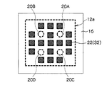
図1(A)に示す断面図には、吸引孔18A、18Bしか図示されていないが、図1(B)に示すように、略直方体状のボンディングヘッド12は4つの吸引孔18A〜18Dを備えている。これら吸引孔18A〜18Dの吸着面12a側の開口の各々が、吸着口20A〜20Dである。吸着口20A〜20Dの各々は、外周形状が略円形とされている。なお、吸引孔18A〜18Dを区別する必要が無い場合には吸引孔18と総称し、吸着口20A〜20Dを区別する必要が無い場合には吸着口20と総称する。
Although only the suction holes 18A and 18B are shown in the cross-sectional view shown in FIG. 1A, the substantially rectangular
半導体チップ30は、平面視が矩形状の小さな薄板である。半導体チップ30の表面側には、表面電極として複数のバンプ電極32が設けられている。一方、半導体チップ30の裏面側には、複数のバンプ電極32に対向する位置に、裏面電極として複数のバンプ電極34が設けられている。互いに対向するバンプ電極32とバンプ電極34とは、半導体チップ30の基板を貫通する貫通電極36により電気的に接続されている。ボンディングヘッド12の吸着口20A〜20Dの各々は、半導体チップ30のバンプ電極32がパッケージ基板16のバンプ電極22と接合される接合領域を避けるように配置されている。吸着口20の配置条件については後述する。
The
上記のボンディング装置10では、半導体チップ30は、ボンディングヘッド12の吸着口20A〜20Dからの吸引により吸着面12aに吸着される。この吸着状態で、半導体チップ30は、半導体チップ30のバンプ電極32とパッケージ基板16のバンプ電極22とが対向する位置まで搬送される。その後、ボンディングヘッド12を矢印方向に移動させて、バンプ電極32とバンプ電極22とを接触させる。このとき、ボンディングヘッド12及びステージ14の少なくとも一方に、加熱、荷重、超音波等を加えるなどして、バンプ電極32とバンプ電極22とが接合される。これによりパッケージ基板16に半導体チップ30が搭載された半導体装置が製造される。
In the
<吸着口の配置>
ここで、ボンディングヘッド12の吸着口20の配置条件を詳細に説明する。
まず、半導体チップのバンプ電極の配置について説明する。図2(A)は表面及び裏面にバンプ電極が形成された半導体チップの断面図であり、図2(B)は裏面側のバンプ電極の配置を示す平面図であり、図2(C)は表面側のバンプ電極の配置を示す平面図である。図2(A)は図2(B)及び(C)のC−C線断面図に相当する。なお、図面上は、裏面側のバンプ電極を四角で示し、表面側のバンプ電極を円で示して区別しているが、これらの標記はバンプ電極の形状を限定するものではない。
<Suction port arrangement>
Here, the arrangement conditions of the suction port 20 of the
First, the arrangement of the bump electrodes of the semiconductor chip will be described. 2A is a cross-sectional view of a semiconductor chip in which bump electrodes are formed on the front surface and the back surface, FIG. 2B is a plan view showing the arrangement of bump electrodes on the back surface side, and FIG. It is a top view which shows arrangement | positioning of the bump electrode of the surface side. 2A corresponds to a cross-sectional view taken along the line CC of FIGS. 2B and 2C. In the drawing, the bump electrodes on the back surface side are indicated by squares and the bump electrodes on the front surface side are indicated by circles to distinguish them, but these marks do not limit the shape of the bump electrodes.
図2(A)〜(C)は半導体チップのバンプ電極の配置を模式的に表すものである。実際には、半導体チップ30の表面に、さらに多数のバンプ電極が形成されている。図2(B)に示す例では、半導体チップ30の裏面側には、21個のバンプ電極34が形成されている。これらバンプ電極34は、2行2列目、2行4列目、4行2列目、4行4列目の4つを除いた、5行5列のマトリクス状に配列されている。
2A to 2C schematically show the arrangement of bump electrodes of a semiconductor chip. Actually, a larger number of bump electrodes are formed on the surface of the
また、図2(C)に示すように、半導体チップ30の表面側には、基板を介してバンプ電極34と対向する位置にバンプ電極32が設けられている。従って、基本的には、バンプ電極32の個数はバンプ電極34の個数と同数であり、バンプ電極32の配置はバンプ電極34の配置を反転させたものになる。
Further, as shown in FIG. 2C, a
次に、バンプ電極同士が接合される接合領域について説明する。図3(A)はパッケージ基板のバンプ電極の配置を模式的に示す平面図であり、図3(B)はバンプ電極同士が接合される接合領域を模式的に示す平面図である。図3(A)に示すように、パッケージ基板16の表面には、半導体チップ30に対向する領域24内に、17個のバンプ電極22が形成されている。これらバンプ電極22は、1行1列目、1行5列目、2行2列目、2行4列目、4行2列目、4行4列目、5行1列目、5行5列目の8つを除いた、5行5列のマトリクス状に配列されている。
Next, a bonding area where the bump electrodes are bonded will be described. FIG. 3A is a plan view schematically showing the arrangement of bump electrodes on the package substrate, and FIG. 3B is a plan view schematically showing a bonding region where the bump electrodes are bonded to each other. As shown in FIG. 3A, 17
ボンディングヘッド12により、半導体チップ30がパッケージ基板16上にフェイスダウンで配置されると、図3(B)に示すように、互いに対向するバンプ電極32とバンプ電極22とが接合される。このようにパッケージ基板16のバンプ電極22と半導体チップ30のバンプ電極32とが接合される領域が接合領域である。例えば、半導体チップ30の斜線で表示されたバンプ電極32は、パッケージ基板16の黒ベタで表示されたバンプ電極22と接合されるが、半導体チップ30の点線で表示されたバンプ電極32は、対向する位置にバンプ電極が存在しないため、接合領域から除外される。
When the
上記した半導体チップ30のバンプ電極32(表面電極)の配置情報や、パッケージ基板16のバンプ電極22(基板電極)の配置情報は、半導体装置の設計図等から容易に取得することができる。これらを比較して上述した接合領域を求め、吸着口20がこれら接合領域を避けて配置されるように、ボンディングヘッド12が設計されている。
The arrangement information of the bump electrode 32 (surface electrode) of the
図4は接合領域に応じた吸着口のレイアウトを示す図である。例えば、図4に示すように、パッケージ基板16上に配置された半導体チップ30の接合領域を予め想定し、ボンディングヘッド12の吸着面12aに半導体チップ30の裏面が吸着されたときに、複数の吸着口20がこれら接合領域の間隙に分散して配置されるように、ボンディングヘッド12の構造を設計することができる。なお、ボンディングヘッド12の吸着面12aにおける吸着口20のレイアウトは太い点線で図示した。図4では、吸着面12aを裏側から見ていることになる。
FIG. 4 is a view showing the layout of the suction ports corresponding to the joining regions. For example, as shown in FIG. 4, when a bonding region of the
図1(A)及び(B)に示したボンディングヘッド12は、図3(B)に示した接合領域に応じた吸着口20のレイアウト(図4)に基づいて設計されたものであり、各々が吸着面12aに開口した4つの吸引孔18A〜18Dを備えている。吸引孔18A〜18Dの開口の各々が、吸着口20A〜20Dである。従って、吸着口20A〜20Dは、接合領域と重なることがない。
The
半導体チップ30の裏面側には複数のバンプ電極34(裏面電極)が設けられる。接合領域では、これらバンプ電極34の一部が、バンプ電極32(表面電極)を介してパッケージ基板16のバンプ電極22(基板電極)と接続される。従って、バンプ電極22(基板電極)と接続されるバンプ電極34(裏面電極)が吸引されないように、ボンディングヘッド12で半導体チップ30の裏面側を吸引保持する。即ち、基板電極と接続される裏面電極が設けられる領域以外の裏面側の領域から「複数の吸着領域」が選択され、これらの吸着領域がボンディングヘッド12の吸着口20に吸着される。
A plurality of bump electrodes 34 (back surface electrodes) are provided on the back surface side of the
以上説明したように、本実施の形態では、パッケージ基板上の電極とフリップチップ接続される半導体チップの表面電極及び対応する裏面電極が、ボンディング時に吸引されることがないので、接合されるはずの電極が接合されない等の接合不良の発生を防止することができると共に、吸引による裏面電極の変形も防止することができる。また、本実施の形態では、複数の吸着口で半導体チップを吸着しているので、半導体チップ内に応力差が発生し難く、半導体チップが割れるのを防止することができる。 As described above, in this embodiment, the electrode on the package substrate and the front surface electrode of the semiconductor chip that is flip-chip connected and the corresponding back surface electrode are not attracted at the time of bonding. It is possible to prevent the occurrence of bonding failure such as the electrode not being bonded, and to prevent deformation of the back electrode due to suction. In the present embodiment, since the semiconductor chip is adsorbed by a plurality of adsorbing ports, a stress difference is hardly generated in the semiconductor chip, and the semiconductor chip can be prevented from cracking.
(第2の実施の形態)
第2の実施の形態に係るボンディング装置は、ボンディングヘッドの構造以外は第1の実施の形態と同様の構成を備えているので、全体構造の説明は省略し、以下ではボンディングヘッドの構造のみを説明する。図5(A)はボンディングヘッドの吸着面の平面図であり、図5(B)は図5(A)のD−D線断面図である。また、図5(C)は接合領域に応じた吸着口のレイアウトを示す図である。
(Second Embodiment)
Since the bonding apparatus according to the second embodiment has the same configuration as that of the first embodiment except for the structure of the bonding head, description of the overall structure is omitted, and only the structure of the bonding head is described below. explain. 5A is a plan view of the suction surface of the bonding head, and FIG. 5B is a cross-sectional view taken along the line DD of FIG. 5A. FIG. 5C is a diagram showing the layout of the suction ports corresponding to the bonding regions.
第2の実施の形態に係るボンディングヘッド40は、平面視が矩形状の吸着面40aを備えている。また、ボンディングヘッド40には、ボンディングヘッド40を貫通する複数の吸引孔42が設けられている。図5(B)に示す断面図には、吸引孔42A、42Bしか図示されていないが、図5(A)に示すように、ボンディングヘッド40は4つの吸引孔42A〜42Dを備えている。吸引孔42A〜42Dの各々は、断面形状が略円形の円柱状とされている。
The
一方、吸着面40a側には、吸着面40aから所定深さで切り欠かれた複数の溝44が設けられている。溝44の溝幅は、吸引孔42の孔径より大きく、バンプ電極の配置ピッチ(通常は50μm)の数倍程度(例えば200μm程度)が好適である。また、深さd2は、深さd1より大幅に小さくてもよい。例えば、深さd1は、直方体状のボンディングヘッド12の高さと略等しくすることができる。これに対し、深さd2は200μm程度が好適である。
On the other hand, on the
図5(B)に示す断面図には、溝44A、44Bしか図示されていないが、図5(A)に示すように、ボンディングヘッド40の吸着面40aには4つの吸引孔42A〜42Dが開口しており、各々の開口について溝44A〜44Dを備えている。溝44Aは吸引孔42Aと連通し、吸引孔42Aから外側に延在するように形成されている。この例では、吸着面40aの一端と平行に延びた溝44Aが形成されている。同様に、溝44Bは吸引孔42Bと連通し、吸引孔42Bから外側に延在するように形成されている。溝44Cは吸引孔42Cと連通し、吸引孔42Cから外側に延在するように形成されている。溝44Dは吸引孔42Dと連通し、吸引孔42Dから外側に延在するように形成されている。
5B, only the
吸引孔42A及び溝44Aの吸着面40a側の開口が、吸着口46Aである。同様に、吸引孔42B及び溝44Bの吸着面40a側の開口が、吸着口46Bである。吸引孔42C及び溝44Cの吸着面40a側の開口が、吸着口46Cである。吸引孔42D及び溝44Dの吸着面40a側の開口が、吸着口46Dである。吸着口46A〜46Dの各々の形状は、円に長方形を重ねた形になる。なお、吸引孔42A〜42Dを区別する必要が無い場合には吸引孔42と総称し、溝44A〜44Dを区別する必要が無い場合には溝44と総称し、吸着口46A〜46Dを区別する必要が無い場合には吸着口46と総称する。
An opening on the
上記のボンディング装置では、半導体チップ30は、ボンディングヘッド40の吸着口46A〜46Dからの吸引により吸着面40aに吸着される。この吸着状態で、半導体チップ30は、半導体チップ30のバンプ電極32とパッケージ基板16のバンプ電極22とが対向する位置まで搬送される。その後、ボンディングヘッド40を移動させて、バンプ電極32とバンプ電極22とを接触させる。ボンディングヘッドによる加圧、加熱等により、バンプ電極32とバンプ電極22とが接合される。
In the above bonding apparatus, the
本実施の形態では、第1の実施の形態と同様に、半導体チップ30がパッケージ基板16上にフェイスダウンで配置され、互いに対向するバンプ電極32とバンプ電極22とが接合される場合について、第1の実施の形態と同じ接合領域を想定して(図3(B)参照)、ボンディングヘッド40の吸着面40aに半導体チップ30の裏面が吸着されたときに、複数の吸着口46がこれら接合領域の間隙に分散して配置されるようにした、吸着口46のレイアウトの他の一例を示すものである。
In the present embodiment, as in the first embodiment, when the
なお、吸着口46のレイアウトは太い点線で図示した。図5(C)では、吸着面40aを裏側から見ていることになる。第2の実施の形態に係るボンディングヘッド40は、図3(B)に示した接合領域に応じた吸着口46のレイアウト(図5(C))に基づいて設計されたものであり、各々が吸着面40aに開口した4つの吸着口46A〜46Dを備えている。従って、吸着口46A〜46Dは、接合領域と重なることがない。
The layout of the suction port 46 is shown by a thick dotted line. In FIG. 5C, the
以上説明したように、本実施の形態では、パッケージ基板上の電極とフリップチップ接続される半導体チップの表面電極及び対応する裏面電極が、ボンディング時に吸引されることがないので、接合されるはずの電極が接合されない等の接合不良を防止することができると共に、吸引による裏面電極の変形も防止することができる。また、本実施の形態では、複数の吸着口で半導体チップを吸着しているので、半導体チップ内に応力差が発生し難く、半導体チップが割れるのを防止することができる。 As described above, in this embodiment, the electrode on the package substrate and the front surface electrode of the semiconductor chip that is flip-chip connected and the corresponding back surface electrode are not attracted at the time of bonding. It is possible to prevent bonding failure such as the electrode not being bonded, and to prevent deformation of the back electrode due to suction. In the present embodiment, since the semiconductor chip is adsorbed by a plurality of adsorbing ports, a stress difference is hardly generated in the semiconductor chip, and the semiconductor chip can be prevented from cracking.
加えて、本実施の形態では、吸着面側に吸引口に連結する溝を設け、吸着口の形状を円に長方形を重ねた形状として、吸着面積を増やすことにより吸着力を高めることが可能で、接合の最中に接合時に係る荷重で半導体チップの位置がずれるのを防止することができる。 In addition, in this embodiment, it is possible to increase the suction force by providing a groove connected to the suction port on the suction surface side and increasing the suction area by making the shape of the suction port a circle and a rectangle superimposed. Further, it is possible to prevent the position of the semiconductor chip from being shifted due to the load applied during bonding during the bonding.
(第3の実施の形態)
第3の実施の形態では、第1の実施の形態及び第2の実施の形態とは異なる接合領域を想定して、ボンディングヘッドを設計したものである。また、第3の実施の形態に係るボンディング装置は、ボンディングヘッドの構造以外は第1の実施の形態と同様の構成を備えているので、全体構造の説明は省略し、以下ではボンディングヘッドの構造のみを説明する。
(Third embodiment)
In the third embodiment, a bonding head is designed on the assumption of a bonding region different from that in the first and second embodiments. Since the bonding apparatus according to the third embodiment has the same configuration as that of the first embodiment except for the structure of the bonding head, description of the entire structure is omitted, and the structure of the bonding head is described below. I will explain only.
図6はバンプ電極同士が接合される接合領域を模式的に示す平面図である。図示された接合領域は、5行5列のマトリクスの中央に接合部を備えていない点で、図3(B)に示す接合領域とは相違している。第1の実施の形態と同様に、半導体チップ30がパッケージ基板16上にフェイスダウンで配置され、互いに対向するバンプ電極32とバンプ電極22とが接合される場合について、図6に示す接合領域を想定すると、吸着口の異なるレイアウトが可能になる。
FIG. 6 is a plan view schematically showing a bonding region where the bump electrodes are bonded to each other. The illustrated bonding region is different from the bonding region shown in FIG. 3B in that the bonding region is not provided at the center of the matrix of 5 rows and 5 columns. Similar to the first embodiment, when the
即ち、図6に示す接合領域を想定すると、ボンディングヘッドの設計の自由度が大きくなる。図8は接合領域に応じた吸着口のレイアウトを示す図である。例えば、図8に示すように、図6に示す接合領域を避けて、吸着面50aの対角線方向に延びた吸着口を設けることも可能である。以下に具体的に説明する。
That is, assuming the bonding region shown in FIG. 6, the degree of freedom in designing the bonding head is increased. FIG. 8 is a view showing a layout of the suction ports corresponding to the joining regions. For example, as shown in FIG. 8, it is possible to provide a suction port extending in the diagonal direction of the
図7(A)はボンディングヘッドの吸着面の平面図であり、図7(B)は図7(A)のE−E線断面図である。第3の実施の形態に係るボンディングヘッド50は、平面視が矩形状の吸着面50aを備えている。また、ボンディングヘッド50には、吸着面50aとは反対側の表面から深さd3で柱状に掘り下げられた吸引孔52が設けられている。図7(A)に示すように、吸引孔52は、断面形状が略円形の円柱状とされている。
FIG. 7A is a plan view of the suction surface of the bonding head, and FIG. 7B is a cross-sectional view taken along the line EE of FIG. The
一方、吸着面50a側には、吸着面50aから深さd4で切り欠かれた複数の溝54が設けられている。溝54の溝幅は、バンプ電極の配置ピッチ(通常は50μm)の数倍程度(例えば200μm程度)が好適である。また、深さd4は、深さd3より大幅に小さくてもよい。深さd3は、直方体状のボンディングヘッド12の高さと略等しくすることができる。これに対し、深さd4は200μm程度が好適である。図7(B)に示す断面図には、溝54Aしか図示されていないが、図7(A)に示すように、ボンディングヘッド50は2つの溝54Aと溝54Bを備えている。溝54A及び溝54Bの各々は、吸引孔52と連通するように形成されている。
On the other hand, on the
溝54Aと溝54Bの吸着面50a側の開口の各々が、吸着口56A、56Bである。吸着口56A及び吸着口56Bの各々は、外周形状が、長辺が吸着面50aの対角線方向に延びた帯状とされている。吸着口56Aと吸着口56Bとは、互いに交差(略直交)するように配置されている。なお、溝54A、溝54Bを区別する必要が無い場合には溝54と総称し、吸着口56A、吸着口56Bを区別する必要が無い場合には吸着口56と総称する。
The openings on the
上記のボンディング装置では、半導体チップ30は、ボンディングヘッド50の吸着口56A及び吸着口56Bからの吸引により吸着面50aに吸着される。この吸着状態で、半導体チップ30は、半導体チップ30のバンプ電極32とパッケージ基板16のバンプ電極22とが対向する位置まで搬送される。その後、ボンディングヘッド50を移動させて、バンプ電極32とバンプ電極22とを接触させる。ボンディングヘッドによる加圧、加熱等により、バンプ電極32とバンプ電極22とが接合される。
In the above bonding apparatus, the
以上説明したように、本実施の形態では、パッケージ基板上の電極とフリップチップ接続される半導体チップの表面電極及び対応する裏面電極が、ボンディング時に吸引されることがないので、接合されるはずの電極が接合されない等の接合不良を防止することができると共に、吸引による裏面電極の変形も防止することができる。また、本実施の形態では、複数の吸着口で半導体チップを吸着しているので、半導体チップ内に応力差が発生し難く、半導体チップが割れるのを防止することができる。 As described above, in this embodiment, the electrode on the package substrate and the front surface electrode of the semiconductor chip that is flip-chip connected and the corresponding back surface electrode are not attracted at the time of bonding. It is possible to prevent bonding failure such as the electrode not being bonded, and to prevent deformation of the back electrode due to suction. In the present embodiment, since the semiconductor chip is adsorbed by a plurality of adsorbing ports, a stress difference is hardly generated in the semiconductor chip, and the semiconductor chip can be prevented from cracking.
加えて、本実施の形態では、吸引孔を増やさずに、吸着面に設けた吸着溝で吸着領域を広げることが可能になり、ボンディングヘッドの熱分布も良好になる。また、接合の最中に接合時に係る荷重で半導体チップの位置がずれるのを防止することができる。 In addition, in the present embodiment, it is possible to widen the suction area with the suction grooves provided on the suction surface without increasing the suction holes, and the heat distribution of the bonding head is also improved. Further, it is possible to prevent the position of the semiconductor chip from being shifted due to the load applied during bonding during the bonding.
(第4の実施の形態)
第4の実施の形態では、第1〜第3の実施の形態とは逆に、ボンディングヘッドの吸着口のレイアウトに応じて、半導体チップの接合領域を設計したものである。また、第4の実施の形態で使用するボンディング装置は、ボンディングヘッドの構造以外は第1の実施の形態と同様の構成を備えているので、全体構造の説明は省略し、以下ではボンディングヘッドの構造と、接合領域の設計方法だけを説明する。
(Fourth embodiment)
In the fourth embodiment, contrary to the first to third embodiments, the bonding area of the semiconductor chip is designed according to the layout of the suction port of the bonding head. Since the bonding apparatus used in the fourth embodiment has the same configuration as that of the first embodiment except for the structure of the bonding head, description of the entire structure is omitted. Only the structure and the design method of the junction region will be described.
図9(A)はボンディングヘッドの吸着面の平面図であり、図9(B)は図9(A)の領域Aの部分拡大図である。第4の実施の形態に係るボンディングヘッド60は、平面視が矩形状の吸着面60aを備えている。また、ボンディングヘッド60には、吸着面60aとは反対側の表面から所定深さ柱状に掘り下げられた吸引孔62が設けられている。吸引孔62は、断面形状が略円形の円柱状とされている。
9A is a plan view of the suction surface of the bonding head, and FIG. 9B is a partially enlarged view of region A in FIG. 9A. The
一方、吸着面60a側には、吸着面60aから所定深さで切り欠かれた複数の溝64が設けられている。溝64の溝幅は、およそバンプ電極の配置ピッチの数倍程度である。例えば、200μm程度が好適である。溝64の溝深さは、例えば、200μm程度が好適である。この例では、図9(A)に示すように、ボンディングヘッド60は6つの溝64A〜溝64Fを備えている。溝64A〜溝64Fの各々は、吸引孔62と連通するように形成されている。
On the other hand, on the
溝64A〜溝64Fの吸着面60a側の開口の各々が、吸着口66A〜66Fである。吸着口66A及び吸着口66Bの各々は、外周形状が、長辺が吸着面60aの対角線方向に延びた帯状とされている。吸着口66Aと吸着口66Bとは、互いに交差(略直交)するように配置されている。
The openings on the
また、吸着口66C〜66Fの各々は、外周形状が、長辺が吸着面60aの対角線と平行な方向に延びた帯状とされている。吸着口66Cと吸着口66Dとは、吸着口66Aと交差(略直交)するように配置されている。また、吸着口66Eと吸着口66Fとは、吸着口66Bと交差(略直交)するように配置されている。なお、溝64A〜溝64Fを区別する必要が無い場合には溝64と総称し、吸着口66A〜66Fを区別する必要が無い場合には吸着口66と総称する。
Further, each of the
上述したとおり、半導体チップ30のバンプ電極32とパッケージ基板16のバンプ電極22とは、吸着口66A〜66Fが半導体チップ30に吸着する部分を避けて接合するように、予め設計され、配置されている。例えば、図9(B)に示すように、領域Aでは、バンプ電極32とバンプ電極22とが接合される接合領域が、吸着口66A及び吸着口66Cと重ならないように、その周囲に配置されている。従って、接合領域が吸着口66A〜66Fによって吸引されることはない。
As described above, the
即ち、ボンディングヘッド60の吸着口66に吸着させる半導体チップ30の裏面側の領域(吸着領域)が予め定められており、この吸着領域以外の裏面側の領域に、パッケージ基板16のバンプ電極22(基板電極)と接続されるバンプ電極34(裏面電極)を形成する。
That is, a region on the back side of the semiconductor chip 30 (suction region) to be attracted to the suction port 66 of the
上記のボンディング装置では、半導体チップ30は、ボンディングヘッド60の吸着口66A〜66Fからの吸引により吸着面60aに吸着される。この吸着状態で、半導体チップ30は、半導体チップ30のバンプ電極32とパッケージ基板16のバンプ電極22とが対向する位置まで搬送される。その後、ボンディングヘッド60を移動させて、バンプ電極32とバンプ電極22とを接触させる。ボンディングヘッドによる加圧、加熱等により、バンプ電極32とバンプ電極22とが接合される。
In the above bonding apparatus, the
以上説明したように、本実施の形態では、パッケージ基板上の電極とフリップチップ接続される半導体チップの表面電極及び対応する裏面電極が、ボンディング時に吸引されることがないので、接合されるはずの電極が接合されない等の接合不良を防止することができると共に、吸引による裏面電極の変形も防止することができる。また、本実施の形態では、複数の吸着口で半導体チップを吸着しているので、半導体チップ内に応力差が発生し難く、半導体チップが割れるのを防止することができる。 As described above, in this embodiment, the electrode on the package substrate and the front surface electrode of the semiconductor chip that is flip-chip connected and the corresponding back surface electrode are not attracted at the time of bonding. It is possible to prevent bonding failure such as the electrode not being bonded, and to prevent deformation of the back electrode due to suction. In the present embodiment, since the semiconductor chip is adsorbed by a plurality of adsorbing ports, a stress difference is hardly generated in the semiconductor chip, and the semiconductor chip can be prevented from cracking.
特に、本実施の形態では、ボンディングヘッドの吸着口のレイアウトに応じて、半導体チップの接合領域を設計するので、半導体チップの周辺まで吸着溝を広げることで、半導体チップの全体を吸着することが可能になる。これにより、半導体チップ内に応力差がより発生し難い。また、接合の最中に接合時に係る荷重で半導体チップの位置がずれるのを防止することができる。更に、吸引孔を増やさずに吸着領域を広げることが可能になり、ボンディングヘッドの熱分布も良好になる。 In particular, in the present embodiment, the bonding area of the semiconductor chip is designed according to the layout of the suction port of the bonding head, so that the entire semiconductor chip can be sucked by expanding the suction groove to the periphery of the semiconductor chip. It becomes possible. Thereby, a stress difference is less likely to occur in the semiconductor chip. Further, it is possible to prevent the position of the semiconductor chip from being shifted due to the load applied during bonding during the bonding. Furthermore, it is possible to widen the suction area without increasing the number of suction holes, and the heat distribution of the bonding head is also improved.
10 ボンディング装置
12 ボンディングヘッド
12a 吸着面
14 ステージ
16 パッケージ基板
18 吸引孔
20 吸着口
22 バンプ電極
24 領域
30 半導体チップ
32 バンプ電極
34 バンプ電極
36 貫通電極
40 ボンディングヘッド
40a 吸着面
42 吸引孔
44 溝
46 吸着口
50 ボンディングヘッド
50a 吸着面
52 吸引孔
54 溝
56 吸着口
60 ボンディングヘッド
60a 吸着面
62 吸引孔
64 溝
66 吸着口
100 ボンディングヘッド
102 貫通孔
104 吸着口
DESCRIPTION OF
Claims (11)
前記基板の電極と接合される前記半導体チップの表面電極と接続された裏面電極が設けられた領域以外の前記裏面側の領域から選択された複数の吸着領域を、保持部材に吸着させて、前記半導体チップを裏面側から保持する工程と、
前記保持部材を移動させて、保持された前記半導体チップの表面電極と前記基板の電極との位置を合わせ、前記半導体チップと基板とを接合する工程と、
を含むことを特徴とする半導体装置の製造方法。 A semiconductor chip comprising a front surface electrode provided on the front surface side and a back surface electrode provided on the back surface side so as to face the front surface electrode and electrically connected to the front surface electrode is mounted on a substrate. A semiconductor device manufacturing method for manufacturing a semiconductor device,
A plurality of adsorption regions selected from the region on the back surface side other than the region provided with the back electrode connected to the surface electrode of the semiconductor chip to be bonded to the electrode of the substrate are adsorbed to a holding member, and Holding the semiconductor chip from the back side;
Moving the holding member, aligning the position of the held surface electrode of the semiconductor chip and the electrode of the substrate, and bonding the semiconductor chip and the substrate;
A method for manufacturing a semiconductor device, comprising:
前記基板の電極と接合される前記半導体チップの表面電極と接続された裏面電極が設けられた領域以外の前記裏面側の領域から、保持部材に吸着させる複数の吸着領域を選択する工程と、
前記複数の吸着領域を保持部材に吸着させて、前記半導体チップを裏面側から保持する工程と、
保持された前記半導体チップを前記基板上に載置して、前記半導体チップの表面電極と基板の電極とを接合する工程と、
を含むことを特徴とする半導体装置の製造方法。 A semiconductor chip comprising a front surface electrode provided on the front surface side and a back surface electrode provided on the back surface side so as to face the front surface electrode and electrically connected to the front surface electrode is mounted on a substrate. A semiconductor device manufacturing method for manufacturing a semiconductor device,
Selecting a plurality of adsorption regions to be adsorbed to the holding member from the region on the back surface side other than the region provided with the back electrode connected to the surface electrode of the semiconductor chip to be bonded to the electrode of the substrate;
Adsorbing the plurality of adsorption regions to a holding member, and holding the semiconductor chip from the back side;
Placing the held semiconductor chip on the substrate and bonding the surface electrode of the semiconductor chip and the electrode of the substrate;
A method for manufacturing a semiconductor device, comprising:
前記半導体チップを裏面側から保持する保持部材に吸着させる複数の吸着領域以外の前記裏面側の領域に、前記基板の電極と接合される前記半導体チップの表面電極と接続された裏面電極を形成する工程と、
前記複数の吸着領域を保持部材に吸着させて、前記半導体チップを裏面側から保持する工程と、
前記保持部材を移動させて、保持された前記半導体チップの表面電極と前記基板の電極との位置を合わせ、前記半導体チップと基板とを接合する工程と、
を含むことを特徴とする半導体装置の製造方法。 Forming a semiconductor chip comprising a surface electrode provided on the front surface side and a back electrode provided on the back surface side so as to face the surface electrode and electrically connected to the surface electrode; A method of manufacturing a semiconductor device for mounting and manufacturing a semiconductor device,
A back electrode connected to the front surface electrode of the semiconductor chip to be bonded to the electrode of the substrate is formed in a region on the back surface other than the plurality of suction regions for adsorbing the holding member holding the semiconductor chip from the back surface side. Process,
Adsorbing the plurality of adsorption regions to a holding member, and holding the semiconductor chip from the back side;
Moving the holding member, aligning the position of the held surface electrode of the semiconductor chip and the electrode of the substrate, and bonding the semiconductor chip and the substrate;
A method for manufacturing a semiconductor device, comprising:
前記基板の電極と接合される前記半導体チップの表面電極と接続された裏面電極が設けられた領域以外の前記裏面側の領域に存在する複数の吸着領域を吸着して、前記半導体チップを裏面側から保持するように、複数の吸着口が形成された保持部材と、
保持された前記半導体チップの表面電極と前記基板の電極との位置を合わせし、前記半導体チップと基板とが接合されるように、前記保持部材を駆動する駆動手段と、
を含むことを特徴とする半導体装置の製造装置。 A semiconductor chip comprising a front surface electrode provided on the front surface side and a back surface electrode provided on the back surface side so as to face the front surface electrode and electrically connected to the front surface electrode is mounted on a substrate. A semiconductor device manufacturing apparatus for manufacturing a semiconductor device,
Adsorbing a plurality of adsorption regions existing in the region on the back side other than the region provided with the back electrode connected to the surface electrode of the semiconductor chip to be joined to the electrode of the substrate, the semiconductor chip is arranged on the back side A holding member formed with a plurality of suction ports so as to hold from,
Driving means for driving the holding member so that the positions of the held surface electrode of the semiconductor chip and the electrode of the substrate are aligned, and the semiconductor chip and the substrate are bonded;
An apparatus for manufacturing a semiconductor device, comprising:
Priority Applications (3)
| Application Number | Priority Date | Filing Date | Title |
|---|---|---|---|
| JP2007322099A JP2009147068A (en) | 2007-12-13 | 2007-12-13 | Semiconductor device manufacturing method and manufacturing apparatus |
| US12/314,117 US8003437B2 (en) | 2007-12-13 | 2008-12-04 | Semiconductor device fabricating method and fabricating apparatus |
| US13/067,804 US8484820B2 (en) | 2007-12-13 | 2011-06-28 | Semiconductor device fabricating method and fabricating apparatus |
Applications Claiming Priority (1)
| Application Number | Priority Date | Filing Date | Title |
|---|---|---|---|
| JP2007322099A JP2009147068A (en) | 2007-12-13 | 2007-12-13 | Semiconductor device manufacturing method and manufacturing apparatus |
Publications (1)
| Publication Number | Publication Date |
|---|---|
| JP2009147068A true JP2009147068A (en) | 2009-07-02 |
Family
ID=40753808
Family Applications (1)
| Application Number | Title | Priority Date | Filing Date |
|---|---|---|---|
| JP2007322099A Pending JP2009147068A (en) | 2007-12-13 | 2007-12-13 | Semiconductor device manufacturing method and manufacturing apparatus |
Country Status (2)
| Country | Link |
|---|---|
| US (2) | US8003437B2 (en) |
| JP (1) | JP2009147068A (en) |
Cited By (3)
| Publication number | Priority date | Publication date | Assignee | Title |
|---|---|---|---|---|
| JP2012221989A (en) * | 2011-04-04 | 2012-11-12 | Elpida Memory Inc | Semiconductor device manufacturing apparatus and semiconductor device manufacturing method |
| JP2014140032A (en) * | 2013-01-21 | 2014-07-31 | Vesi Switzerland Ag | Bonding head having suction member capable of heating and cooling |
| JP2019033188A (en) * | 2017-08-09 | 2019-02-28 | 東レエンジニアリング株式会社 | Mounting device and mounting method and manufacturing method of semiconductor device using the same |
Families Citing this family (9)
| Publication number | Priority date | Publication date | Assignee | Title |
|---|---|---|---|---|
| DE102012101581A1 (en) * | 2012-02-27 | 2013-08-29 | Optotech Optikmaschinen Gmbh | Apparatus and method for processing spectacle lens blanks |
| USD758372S1 (en) * | 2013-03-13 | 2016-06-07 | Nagrastar Llc | Smart card interface |
| USD759022S1 (en) * | 2013-03-13 | 2016-06-14 | Nagrastar Llc | Smart card interface |
| USD729808S1 (en) * | 2013-03-13 | 2015-05-19 | Nagrastar Llc | Smart card interface |
| DE102015102899B4 (en) | 2015-02-27 | 2018-02-01 | Optotech Optikmaschinen Gmbh | Milling device for the production of spectacle lenses with two milling stations |
| USD780763S1 (en) * | 2015-03-20 | 2017-03-07 | Nagrastar Llc | Smart card interface |
| USD864968S1 (en) * | 2015-04-30 | 2019-10-29 | Echostar Technologies L.L.C. | Smart card interface |
| KR20180087536A (en) * | 2017-01-24 | 2018-08-02 | 삼성디스플레이 주식회사 | Connecting device and circuit chip connecting method using connecting device |
| CN113097074B (en) * | 2021-04-06 | 2024-02-09 | 南京大学 | Two-dimensional material patterned electrode integration and surface passivation method |
Citations (6)
| Publication number | Priority date | Publication date | Assignee | Title |
|---|---|---|---|---|
| JPH08213427A (en) * | 1995-02-07 | 1996-08-20 | Sharp Corp | Semiconductor chip and multi-chip semiconductor module |
| JPH0936181A (en) * | 1995-07-21 | 1997-02-07 | Shibuya Kogyo Co Ltd | Bonding tool |
| JPH11307580A (en) * | 1998-04-17 | 1999-11-05 | Nec Corp | Tool for chucking semiconductor chip and manufacture of semiconductor device use the tool |
| JP2001068511A (en) * | 1999-06-22 | 2001-03-16 | Murata Mfg Co Ltd | Method of mounting electronic device element and manufacture of surface acoustic wave device |
| JP2002313843A (en) * | 2001-04-18 | 2002-10-25 | Sharp Corp | Connection device |
| JP2005347621A (en) * | 2004-06-04 | 2005-12-15 | Matsushita Electric Ind Co Ltd | Electronic component mounting tool |
Family Cites Families (6)
| Publication number | Priority date | Publication date | Assignee | Title |
|---|---|---|---|---|
| JPS6329539A (en) | 1986-07-23 | 1988-02-08 | Hitachi Ltd | Vacuum suction apparatus |
| JPH0766268A (en) | 1993-08-20 | 1995-03-10 | Sony Corp | Suction device of semiconductor chip |
| JP2000357711A (en) * | 1999-06-15 | 2000-12-26 | Sony Corp | Manufacturing jig and manufacturing method of semiconductor device |
| US20030001286A1 (en) * | 2000-01-28 | 2003-01-02 | Ryoichi Kajiwara | Semiconductor package and flip chip bonding method therein |
| US6617573B2 (en) * | 2001-10-25 | 2003-09-09 | Ushiodenki Kabushiki Kaisha | Carrier device having a carrier surface with an opening for connecting with grooves |
| JP2004039736A (en) * | 2002-07-01 | 2004-02-05 | Shinko Electric Ind Co Ltd | Device and method for mounting semiconductor chip |
-
2007
- 2007-12-13 JP JP2007322099A patent/JP2009147068A/en active Pending
-
2008
- 2008-12-04 US US12/314,117 patent/US8003437B2/en active Active
-
2011
- 2011-06-28 US US13/067,804 patent/US8484820B2/en active Active
Patent Citations (6)
| Publication number | Priority date | Publication date | Assignee | Title |
|---|---|---|---|---|
| JPH08213427A (en) * | 1995-02-07 | 1996-08-20 | Sharp Corp | Semiconductor chip and multi-chip semiconductor module |
| JPH0936181A (en) * | 1995-07-21 | 1997-02-07 | Shibuya Kogyo Co Ltd | Bonding tool |
| JPH11307580A (en) * | 1998-04-17 | 1999-11-05 | Nec Corp | Tool for chucking semiconductor chip and manufacture of semiconductor device use the tool |
| JP2001068511A (en) * | 1999-06-22 | 2001-03-16 | Murata Mfg Co Ltd | Method of mounting electronic device element and manufacture of surface acoustic wave device |
| JP2002313843A (en) * | 2001-04-18 | 2002-10-25 | Sharp Corp | Connection device |
| JP2005347621A (en) * | 2004-06-04 | 2005-12-15 | Matsushita Electric Ind Co Ltd | Electronic component mounting tool |
Cited By (3)
| Publication number | Priority date | Publication date | Assignee | Title |
|---|---|---|---|---|
| JP2012221989A (en) * | 2011-04-04 | 2012-11-12 | Elpida Memory Inc | Semiconductor device manufacturing apparatus and semiconductor device manufacturing method |
| JP2014140032A (en) * | 2013-01-21 | 2014-07-31 | Vesi Switzerland Ag | Bonding head having suction member capable of heating and cooling |
| JP2019033188A (en) * | 2017-08-09 | 2019-02-28 | 東レエンジニアリング株式会社 | Mounting device and mounting method and manufacturing method of semiconductor device using the same |
Also Published As
| Publication number | Publication date |
|---|---|
| US20090155953A1 (en) | 2009-06-18 |
| US8003437B2 (en) | 2011-08-23 |
| US20110258849A1 (en) | 2011-10-27 |
| US8484820B2 (en) | 2013-07-16 |
Similar Documents
| Publication | Publication Date | Title |
|---|---|---|
| JP2009147068A (en) | Semiconductor device manufacturing method and manufacturing apparatus | |
| KR100809696B1 (en) | A Multi chip package stacked a plurality of semiconductor chips having different size and method of manufacturing the same | |
| US8673686B2 (en) | Chip package structure and manufacturing method thereof | |
| JP6338555B2 (en) | Adsorption mechanism, adsorption method, production apparatus and production method | |
| JP5116615B2 (en) | Positioning jig unit and soldering method | |
| JP2009099922A (en) | Laminated semiconductor package, and manufacturing method thereof | |
| JP2010103195A (en) | Multilayer type semiconductor device and method of manufacturing the same | |
| JP5073599B2 (en) | Semiconductor chip inspection jig, inspection apparatus and inspection method, and semiconductor device manufacturing method | |
| JP2002141459A (en) | Semiconductor device and its manufacturing method | |
| US20150231723A1 (en) | Solder ball attaching apparatus, flux dotting apparatus, and method of manufacturing semiconductor package | |
| JP2011129821A (en) | Pickup device for semiconductor chip, and method of manufacturing semiconductor chip | |
| JP4637720B2 (en) | Semiconductor device and manufacturing method thereof | |
| WO2014167867A1 (en) | Laminated semiconductor device and laminated semiconductor manufacturing method | |
| JP5315913B2 (en) | Manufacturing method of laminated semiconductor device | |
| JP5953068B2 (en) | Electronic component placement table and die bonder equipped with the same table | |
| TWI501349B (en) | Wafer adsorption head | |
| KR20120005341A (en) | Semiconductor chip and package | |
| JP5187299B2 (en) | Manufacturing method of semiconductor device | |
| KR102056186B1 (en) | Pickup apparatus of semiconductor package | |
| JP2001244285A (en) | Fine ball arranged plate and device | |
| JP2007149735A (en) | Pickup jig for semiconductor element and its manufacturing process | |
| CN115939000A (en) | Chip bearing device and chip and wafer bonding method | |
| JP2014157904A (en) | Electronic component placing table and die bonder including the same | |
| KR100668847B1 (en) | Package stack | |
| JP2010192648A (en) | Debonding apparatus and debonding method |
Legal Events
| Date | Code | Title | Description |
|---|---|---|---|
| A977 | Report on retrieval |
Free format text: JAPANESE INTERMEDIATE CODE: A971007 Effective date: 20091111 |
|
| A131 | Notification of reasons for refusal |
Free format text: JAPANESE INTERMEDIATE CODE: A131 Effective date: 20091117 |
|
| A521 | Written amendment |
Free format text: JAPANESE INTERMEDIATE CODE: A523 Effective date: 20100115 |
|
| A02 | Decision of refusal |
Free format text: JAPANESE INTERMEDIATE CODE: A02 Effective date: 20100921 |