JP2009137776A - GaAs SEMICONDUCTOR SUBSTRATE AND ITS MANUFACTURING METHOD, AND GROUP III-V COMPOUND SEMICONDUCTOR DEVICE AND ITS MANUFACTURING METHOD - Google Patents
GaAs SEMICONDUCTOR SUBSTRATE AND ITS MANUFACTURING METHOD, AND GROUP III-V COMPOUND SEMICONDUCTOR DEVICE AND ITS MANUFACTURING METHOD Download PDFInfo
- Publication number
- JP2009137776A JP2009137776A JP2007313286A JP2007313286A JP2009137776A JP 2009137776 A JP2009137776 A JP 2009137776A JP 2007313286 A JP2007313286 A JP 2007313286A JP 2007313286 A JP2007313286 A JP 2007313286A JP 2009137776 A JP2009137776 A JP 2009137776A
- Authority
- JP
- Japan
- Prior art keywords
- gaas semiconductor
- semiconductor substrate
- main surface
- gaas
- cleaning
- Prior art date
- Legal status (The legal status is an assumption and is not a legal conclusion. Google has not performed a legal analysis and makes no representation as to the accuracy of the status listed.)
- Pending
Links
- 239000004065 semiconductor Substances 0.000 title claims abstract description 235
- 229910001218 Gallium arsenide Inorganic materials 0.000 title claims abstract description 153
- 239000000758 substrate Substances 0.000 title claims abstract description 114
- 150000001875 compounds Chemical class 0.000 title claims abstract description 61
- 238000004519 manufacturing process Methods 0.000 title claims abstract description 32
- 238000004140 cleaning Methods 0.000 claims abstract description 99
- 125000001309 chloro group Chemical group Cl* 0.000 claims abstract description 66
- 238000000034 method Methods 0.000 claims abstract description 61
- 230000008569 process Effects 0.000 claims abstract description 39
- VEXZGXHMUGYJMC-UHFFFAOYSA-N Hydrochloric acid Chemical compound Cl VEXZGXHMUGYJMC-UHFFFAOYSA-N 0.000 claims abstract description 34
- 238000007689 inspection Methods 0.000 claims abstract description 29
- 238000005498 polishing Methods 0.000 claims abstract description 21
- 239000002253 acid Substances 0.000 claims abstract description 11
- 229910052801 chlorine Inorganic materials 0.000 claims description 61
- XLYOFNOQVPJJNP-UHFFFAOYSA-N water Substances O XLYOFNOQVPJJNP-UHFFFAOYSA-N 0.000 claims description 20
- OKTJSMMVPCPJKN-UHFFFAOYSA-N Carbon Chemical compound [C] OKTJSMMVPCPJKN-UHFFFAOYSA-N 0.000 claims description 16
- 239000003595 mist Substances 0.000 claims description 9
- 150000007513 acids Chemical class 0.000 claims description 2
- 230000003746 surface roughness Effects 0.000 claims description 2
- 239000003513 alkali Substances 0.000 abstract description 11
- 238000007517 polishing process Methods 0.000 abstract description 9
- 230000000052 comparative effect Effects 0.000 description 20
- KFZMGEQAYNKOFK-UHFFFAOYSA-N Isopropanol Chemical compound CC(C)O KFZMGEQAYNKOFK-UHFFFAOYSA-N 0.000 description 12
- 238000001035 drying Methods 0.000 description 10
- QGZKDVFQNNGYKY-UHFFFAOYSA-N Ammonia Chemical compound N QGZKDVFQNNGYKY-UHFFFAOYSA-N 0.000 description 8
- ZAMOUSCENKQFHK-UHFFFAOYSA-N Chlorine atom Chemical compound [Cl] ZAMOUSCENKQFHK-UHFFFAOYSA-N 0.000 description 7
- 239000000460 chlorine Substances 0.000 description 7
- 239000011347 resin Substances 0.000 description 5
- 229920005989 resin Polymers 0.000 description 5
- MHAJPDPJQMAIIY-UHFFFAOYSA-N Hydrogen peroxide Chemical compound OO MHAJPDPJQMAIIY-UHFFFAOYSA-N 0.000 description 4
- 239000006061 abrasive grain Substances 0.000 description 4
- 229910021529 ammonia Inorganic materials 0.000 description 4
- 230000004888 barrier function Effects 0.000 description 4
- -1 nitride compound Chemical class 0.000 description 4
- WGTYBPLFGIVFAS-UHFFFAOYSA-M tetramethylammonium hydroxide Chemical compound [OH-].C[N+](C)(C)C WGTYBPLFGIVFAS-UHFFFAOYSA-M 0.000 description 4
- LFQSCWFLJHTTHZ-UHFFFAOYSA-N Ethanol Chemical compound CCO LFQSCWFLJHTTHZ-UHFFFAOYSA-N 0.000 description 3
- 229910052782 aluminium Inorganic materials 0.000 description 3
- QVGXLLKOCUKJST-UHFFFAOYSA-N atomic oxygen Chemical compound [O] QVGXLLKOCUKJST-UHFFFAOYSA-N 0.000 description 3
- 239000000919 ceramic Substances 0.000 description 3
- 238000005229 chemical vapour deposition Methods 0.000 description 3
- 229910052733 gallium Inorganic materials 0.000 description 3
- 229910052751 metal Inorganic materials 0.000 description 3
- 239000002184 metal Substances 0.000 description 3
- 238000002488 metal-organic chemical vapour deposition Methods 0.000 description 3
- 239000003960 organic solvent Substances 0.000 description 3
- 239000001301 oxygen Substances 0.000 description 3
- 229910052760 oxygen Inorganic materials 0.000 description 3
- 229910021642 ultra pure water Inorganic materials 0.000 description 3
- 239000012498 ultrapure water Substances 0.000 description 3
- 238000005406 washing Methods 0.000 description 3
- IJGRMHOSHXDMSA-UHFFFAOYSA-N Atomic nitrogen Chemical compound N#N IJGRMHOSHXDMSA-UHFFFAOYSA-N 0.000 description 2
- 229910017401 Au—Ge Inorganic materials 0.000 description 2
- VEXZGXHMUGYJMC-UHFFFAOYSA-M Chloride anion Chemical compound [Cl-] VEXZGXHMUGYJMC-UHFFFAOYSA-M 0.000 description 2
- 229940123973 Oxygen scavenger Drugs 0.000 description 2
- 239000004698 Polyethylene Substances 0.000 description 2
- 239000004743 Polypropylene Substances 0.000 description 2
- VYPSYNLAJGMNEJ-UHFFFAOYSA-N Silicium dioxide Chemical compound O=[Si]=O VYPSYNLAJGMNEJ-UHFFFAOYSA-N 0.000 description 2
- GWEVSGVZZGPLCZ-UHFFFAOYSA-N Titan oxide Chemical compound O=[Ti]=O GWEVSGVZZGPLCZ-UHFFFAOYSA-N 0.000 description 2
- 230000002378 acidificating effect Effects 0.000 description 2
- 229910052785 arsenic Inorganic materials 0.000 description 2
- 239000008119 colloidal silica Substances 0.000 description 2
- 239000013078 crystal Substances 0.000 description 2
- 229910001873 dinitrogen Inorganic materials 0.000 description 2
- 238000010348 incorporation Methods 0.000 description 2
- 229910052738 indium Inorganic materials 0.000 description 2
- 239000000463 material Substances 0.000 description 2
- 239000000203 mixture Substances 0.000 description 2
- TWNQGVIAIRXVLR-UHFFFAOYSA-N oxo(oxoalumanyloxy)alumane Chemical compound O=[Al]O[Al]=O TWNQGVIAIRXVLR-UHFFFAOYSA-N 0.000 description 2
- 239000002245 particle Substances 0.000 description 2
- 230000035699 permeability Effects 0.000 description 2
- 229910052698 phosphorus Inorganic materials 0.000 description 2
- 239000004417 polycarbonate Substances 0.000 description 2
- 239000000126 substance Substances 0.000 description 2
- VZSRBBMJRBPUNF-UHFFFAOYSA-N 2-(2,3-dihydro-1H-inden-2-ylamino)-N-[3-oxo-3-(2,4,6,7-tetrahydrotriazolo[4,5-c]pyridin-5-yl)propyl]pyrimidine-5-carboxamide Chemical compound C1C(CC2=CC=CC=C12)NC1=NC=C(C=N1)C(=O)NCCC(N1CC2=C(CC1)NN=N2)=O VZSRBBMJRBPUNF-UHFFFAOYSA-N 0.000 description 1
- XEEYBQQBJWHFJM-UHFFFAOYSA-N Iron Chemical compound [Fe] XEEYBQQBJWHFJM-UHFFFAOYSA-N 0.000 description 1
- GRYLNZFGIOXLOG-UHFFFAOYSA-N Nitric acid Chemical compound O[N+]([O-])=O GRYLNZFGIOXLOG-UHFFFAOYSA-N 0.000 description 1
- 238000002441 X-ray diffraction Methods 0.000 description 1
- 230000009471 action Effects 0.000 description 1
- XAGFODPZIPBFFR-UHFFFAOYSA-N aluminium Chemical compound [Al] XAGFODPZIPBFFR-UHFFFAOYSA-N 0.000 description 1
- 239000007864 aqueous solution Substances 0.000 description 1
- 239000012298 atmosphere Substances 0.000 description 1
- 125000004429 atom Chemical group 0.000 description 1
- 230000015556 catabolic process Effects 0.000 description 1
- 229910000420 cerium oxide Inorganic materials 0.000 description 1
- 239000012459 cleaning agent Substances 0.000 description 1
- 238000001816 cooling Methods 0.000 description 1
- 230000007547 defect Effects 0.000 description 1
- 238000006731 degradation reaction Methods 0.000 description 1
- 238000007791 dehumidification Methods 0.000 description 1
- 229910003460 diamond Inorganic materials 0.000 description 1
- 239000010432 diamond Substances 0.000 description 1
- 238000005530 etching Methods 0.000 description 1
- 230000005284 excitation Effects 0.000 description 1
- 239000011888 foil Substances 0.000 description 1
- 238000000227 grinding Methods 0.000 description 1
- 229910021478 group 5 element Inorganic materials 0.000 description 1
- 239000012535 impurity Substances 0.000 description 1
- 239000007788 liquid Substances 0.000 description 1
- 238000012986 modification Methods 0.000 description 1
- 230000004048 modification Effects 0.000 description 1
- 229910017604 nitric acid Inorganic materials 0.000 description 1
- BMMGVYCKOGBVEV-UHFFFAOYSA-N oxo(oxoceriooxy)cerium Chemical compound [Ce]=O.O=[Ce]=O BMMGVYCKOGBVEV-UHFFFAOYSA-N 0.000 description 1
- 238000005424 photoluminescence Methods 0.000 description 1
- 229920000515 polycarbonate Polymers 0.000 description 1
- 229920000573 polyethylene Polymers 0.000 description 1
- 229920001155 polypropylene Polymers 0.000 description 1
- 239000000843 powder Substances 0.000 description 1
- 238000002360 preparation method Methods 0.000 description 1
- 238000004611 spectroscopical analysis Methods 0.000 description 1
- KKEYFWRCBNTPAC-UHFFFAOYSA-L terephthalate(2-) Chemical compound [O-]C(=O)C1=CC=C(C([O-])=O)C=C1 KKEYFWRCBNTPAC-UHFFFAOYSA-L 0.000 description 1
- 239000004408 titanium dioxide Substances 0.000 description 1
- 238000001771 vacuum deposition Methods 0.000 description 1
- 238000007738 vacuum evaporation Methods 0.000 description 1
Images


Classifications
-
- H—ELECTRICITY
- H01—ELECTRIC ELEMENTS
- H01L—SEMICONDUCTOR DEVICES NOT COVERED BY CLASS H10
- H01L29/00—Semiconductor devices specially adapted for rectifying, amplifying, oscillating or switching and having potential barriers; Capacitors or resistors having potential barriers, e.g. a PN-junction depletion layer or carrier concentration layer; Details of semiconductor bodies or of electrodes thereof ; Multistep manufacturing processes therefor
- H01L29/02—Semiconductor bodies ; Multistep manufacturing processes therefor
- H01L29/06—Semiconductor bodies ; Multistep manufacturing processes therefor characterised by their shape; characterised by the shapes, relative sizes, or dispositions of the semiconductor regions ; characterised by the concentration or distribution of impurities within semiconductor regions
- H01L29/0657—Semiconductor bodies ; Multistep manufacturing processes therefor characterised by their shape; characterised by the shapes, relative sizes, or dispositions of the semiconductor regions ; characterised by the concentration or distribution of impurities within semiconductor regions characterised by the shape of the body
-
- H—ELECTRICITY
- H01—ELECTRIC ELEMENTS
- H01L—SEMICONDUCTOR DEVICES NOT COVERED BY CLASS H10
- H01L29/00—Semiconductor devices specially adapted for rectifying, amplifying, oscillating or switching and having potential barriers; Capacitors or resistors having potential barriers, e.g. a PN-junction depletion layer or carrier concentration layer; Details of semiconductor bodies or of electrodes thereof ; Multistep manufacturing processes therefor
- H01L29/02—Semiconductor bodies ; Multistep manufacturing processes therefor
- H01L29/04—Semiconductor bodies ; Multistep manufacturing processes therefor characterised by their crystalline structure, e.g. polycrystalline, cubic or particular orientation of crystalline planes
- H01L29/045—Semiconductor bodies ; Multistep manufacturing processes therefor characterised by their crystalline structure, e.g. polycrystalline, cubic or particular orientation of crystalline planes by their particular orientation of crystalline planes
-
- H—ELECTRICITY
- H01—ELECTRIC ELEMENTS
- H01L—SEMICONDUCTOR DEVICES NOT COVERED BY CLASS H10
- H01L21/00—Processes or apparatus adapted for the manufacture or treatment of semiconductor or solid state devices or of parts thereof
- H01L21/02—Manufacture or treatment of semiconductor devices or of parts thereof
- H01L21/02104—Forming layers
- H01L21/02365—Forming inorganic semiconducting materials on a substrate
- H01L21/02367—Substrates
- H01L21/0237—Materials
- H01L21/02387—Group 13/15 materials
- H01L21/02395—Arsenides
-
- H—ELECTRICITY
- H01—ELECTRIC ELEMENTS
- H01L—SEMICONDUCTOR DEVICES NOT COVERED BY CLASS H10
- H01L21/00—Processes or apparatus adapted for the manufacture or treatment of semiconductor or solid state devices or of parts thereof
- H01L21/02—Manufacture or treatment of semiconductor devices or of parts thereof
- H01L21/02104—Forming layers
- H01L21/02365—Forming inorganic semiconducting materials on a substrate
- H01L21/02367—Substrates
- H01L21/02433—Crystal orientation
-
- H—ELECTRICITY
- H01—ELECTRIC ELEMENTS
- H01L—SEMICONDUCTOR DEVICES NOT COVERED BY CLASS H10
- H01L21/00—Processes or apparatus adapted for the manufacture or treatment of semiconductor or solid state devices or of parts thereof
- H01L21/02—Manufacture or treatment of semiconductor devices or of parts thereof
- H01L21/02104—Forming layers
- H01L21/02365—Forming inorganic semiconducting materials on a substrate
- H01L21/02518—Deposited layers
- H01L21/02521—Materials
- H01L21/02538—Group 13/15 materials
- H01L21/02543—Phosphides
-
- H—ELECTRICITY
- H01—ELECTRIC ELEMENTS
- H01L—SEMICONDUCTOR DEVICES NOT COVERED BY CLASS H10
- H01L21/00—Processes or apparatus adapted for the manufacture or treatment of semiconductor or solid state devices or of parts thereof
- H01L21/02—Manufacture or treatment of semiconductor devices or of parts thereof
- H01L21/02104—Forming layers
- H01L21/02365—Forming inorganic semiconducting materials on a substrate
- H01L21/02656—Special treatments
- H01L21/02658—Pretreatments
Landscapes
- Microelectronics & Electronic Packaging (AREA)
- Engineering & Computer Science (AREA)
- Power Engineering (AREA)
- Condensed Matter Physics & Semiconductors (AREA)
- General Physics & Mathematics (AREA)
- Physics & Mathematics (AREA)
- Ceramic Engineering (AREA)
- Computer Hardware Design (AREA)
- Chemical & Material Sciences (AREA)
- Crystallography & Structural Chemistry (AREA)
- Cleaning Or Drying Semiconductors (AREA)
- Crystals, And After-Treatments Of Crystals (AREA)
- Led Devices (AREA)
- Chemical Vapour Deposition (AREA)
- Testing Or Measuring Of Semiconductors Or The Like (AREA)
Abstract
Description
本発明は、III−V族化合物半導体デバイスの基板として好適に用いられるGaAs半導体基板およびその製造方法、ならびにそのGaAs半導体基板を含むIII−V族化合物半導体デバイスおよびその製造方法に関する。 The present invention relates to a GaAs semiconductor substrate suitably used as a substrate of a III-V compound semiconductor device and a method for manufacturing the same, and a III-V compound semiconductor device including the GaAs semiconductor substrate and a method for manufacturing the same.
GaAs半導体基板は、LED(発光ダイオード)、LD(レーザダイオード)などに用いられるIII−V族化合物半導体デバイスの基板として広く用いられている。ここで、III−V族化合物半導体デバイスは、GaAs半導体基板の主表面上に1層以上のIII−V族化合物半導体層を形成することにより得られる。 GaAs semiconductor substrates are widely used as substrates for III-V group compound semiconductor devices used in LEDs (light emitting diodes), LDs (laser diodes), and the like. Here, the III-V group compound semiconductor device is obtained by forming one or more III-V group compound semiconductor layers on the main surface of the GaAs semiconductor substrate.
GaAs半導体基板の主表面に不純物たる酸性物質が多く存在すると、その主表面が荒れる。このGaAs半導体基板の荒れた主表面上に形成されるIII−V族化合物半導体層には形状欠陥が発生する。このため、III−V族化合物半導体デバイスの歩留まりが低下する。 If there are many acidic substances as impurities on the main surface of the GaAs semiconductor substrate, the main surface becomes rough. A shape defect occurs in the III-V group compound semiconductor layer formed on the rough main surface of the GaAs semiconductor substrate. For this reason, the yield of a III-V group compound semiconductor device falls.
このため、III−V族化合物半導体デバイスの歩留まりを高めるため、たとえば、研磨および洗浄後の表面において1cm2当たりの酸性物質の原子の個数が5×10¹²以下であるIII−V族化合物半導体ウエハおよびその製造方法が提案されている(特許文献1を参照)。
しかし、主表面における塩素原子濃度が高いGaAs半導体基板のその主表面上に少なくとも1層のIII−V族化合物半導体層を成長させてIII−V族化合物半導体デバイスを作製すると、半導体デバイスの歩留まりの低下だけでなく、半導体デバイスの特性が低下することが見出された。特に、3種類以上の元素を含むIII−V族化合物半導体層を成長させる場合に得られる半導体デバイスについて、その特性の低下が大きいことが見出された。 However, when a group III-V compound semiconductor layer is produced by growing at least one group III-V compound semiconductor layer on the main surface of a GaAs semiconductor substrate having a high chlorine atom concentration on the main surface, the yield of the semiconductor device is increased. It has been found that not only the degradation, but also the characteristics of the semiconductor device are degraded. In particular, it has been found that the characteristics of a semiconductor device obtained when growing a III-V group compound semiconductor layer containing three or more kinds of elements are greatly reduced.
そこで、本発明は、その主表面上に少なくとも1層の3種類以上の元素を含むIII−V族化合物半導体層を成長させても高い特性を有するIII−V族化合物半導体デバイスが得られるGaAs半導体基板およびその製造方法を提案することを目的とする。 Accordingly, the present invention provides a GaAs semiconductor capable of obtaining a III-V group compound semiconductor device having high characteristics even when a group III-V group compound semiconductor layer containing at least one layer of three or more elements is grown on its main surface. An object is to propose a substrate and a method for manufacturing the same.
本発明は、主表面が(100)面に対して6〜16°の傾斜角を有し、主表面における塩素原子濃度が1×1013cm-2以下であるGaAs半導体基板である。ここで、主表面における塩素原子濃度は3×1012cm-2以下が好ましい。 The present invention is a GaAs semiconductor substrate in which the main surface has an inclination angle of 6 to 16 ° with respect to the (100) plane and the chlorine atom concentration on the main surface is 1 × 10 13 cm −2 or less. Here, the chlorine atom concentration on the main surface is preferably 3 × 10 12 cm −2 or less.
また、本発明は、上記のGaAs半導体基板の製造方法であって、GaAs半導体ウエハを研磨する研磨工程と、研磨されたGaAs半導体ウエハを洗浄する1次洗浄工程と、1次洗浄後のGaAs半導体ウエハの厚さおよび主表面の粗さを検査する検査工程と、検査後のGaAs半導体ウエハを塩酸以外の酸およびアルカリのいずれかにより洗浄する2次洗浄工程と、を備えるGaAs半導体基板の製造方法である。 The present invention is also a method of manufacturing the above GaAs semiconductor substrate, comprising a polishing step for polishing a GaAs semiconductor wafer, a primary cleaning step for cleaning the polished GaAs semiconductor wafer, and a GaAs semiconductor after the primary cleaning. A method of manufacturing a GaAs semiconductor substrate, comprising: an inspection process for inspecting the thickness of the wafer and the roughness of the main surface; and a secondary cleaning process for cleaning the inspected GaAs semiconductor wafer with an acid other than hydrochloric acid or an alkali. It is.
本発明にかかるGaAs半導体基板の製造方法において、1次洗浄工程は、研磨されたGaAs半導体ウエハを塩酸で洗浄する塩酸洗浄サブ工程を含むことができる。 In the method for manufacturing a GaAs semiconductor substrate according to the present invention, the primary cleaning step may include a hydrochloric acid cleaning sub-step of cleaning the polished GaAs semiconductor wafer with hydrochloric acid.
また、本発明にかかるGaAs半導体基板の製造方法において、1次洗浄工程、検査工程および2次洗浄工程はクリーン室内で行われ、クリーン室内では、室外から純水の霧中を通過して空気が導入され、導入された前記空気は前記活性炭を含んだフィルタを通過して循環され得る。ここで、2次洗浄後におけるクリーン室内の塩素原子含有濃度を、1500ng・m-3以下、さらに、400ng・m-3以下とすることができる。 Further, in the method for manufacturing a GaAs semiconductor substrate according to the present invention, the primary cleaning process, the inspection process and the secondary cleaning process are performed in a clean room, and air is introduced from outside the room through a mist of pure water. The introduced air can then be circulated through a filter containing the activated carbon. Here, the chlorine atom-containing concentration in the clean chamber after the secondary cleaning can be 1500 ng · m −3 or less, and further 400 ng · m −3 or less.
また、本発明は、上記のGaAs半導体基板と、GaAs半導体基板の主表面上に形成されている少なくとも1層の3種類以上の元素を含むIII−V族化合物半導体層と、を備えるIII−V族化合物半導体デバイスである。 According to another aspect of the present invention, there is provided a III-V compound semiconductor layer including the above-described GaAs semiconductor substrate and a III-V group compound semiconductor layer including at least one layer of three or more elements formed on the main surface of the GaAs semiconductor substrate. Group semiconductor device.
また、本発明は、上記のIII−V族化合物半導体デバイスの製造方法であって、GaAs半導体基板を準備する工程と、GaAs半導体基板の主表面上に少なくとも1層の3種類以上の元素を含むIII−V族化合物半導体層を成長させる工程と、を備えるIII−V族化合物半導体デバイスの製造方法である。 The present invention is also a method for manufacturing the above-mentioned III-V group compound semiconductor device, comprising a step of preparing a GaAs semiconductor substrate, and at least one layer of three or more elements on the main surface of the GaAs semiconductor substrate. And a step of growing a group III-V compound semiconductor layer. A method for manufacturing a group III-V compound semiconductor device.
本発明によれば、その主表面上に少なくとも1層の3種類以上の元素を含むIII−V族化合物半導体層を成長させても高い特性を有するIII−V族化合物半導体デバイスが得られるGaAs半導体基板およびその製造方法が提供される。 According to the present invention, a GaAs semiconductor capable of obtaining a group III-V compound semiconductor device having high characteristics even when a group III-V compound semiconductor layer containing at least one layer of three or more elements is grown on its main surface. A substrate and a method for manufacturing the same are provided.
(実施形態1)
本発明にかかるGaAs半導体基板の一実施形態は、図1を参照して、主表面10mが(100)面10aに対して6〜16°の傾斜角θを有し、主表面10mにおける塩素原子濃度が1×1013cm-2以下である。かかるGaAs半導体基板の主表面上に少なくとも1層の3種類以上の元素を含むIII−V族化合物半導体層を成長させても高い特性を有するIII−V族化合物半導体デバイスが得られる。
(Embodiment 1)
Referring to FIG. 1, an embodiment of a GaAs semiconductor substrate according to the present invention has a
本実施形態のGaAs半導体基板10は、その主表面10mが(100)面10aに対して有する傾斜角θが6〜16°であることから、この主表面上に3種類以上の元素を含むIII−V族化合物半導体層を結晶性よくかつ容易に成長させることができる。傾斜角θが6°より小さいと、または、傾斜角θが16°より大きいと、半導体層の結晶性が低下し、III−V族化合物半導体デバイスの特性が低下する。
The GaAs
また、本実施形態のGaAs半導体基板10は、その主表面10mにおける塩素原子濃度が1×1013cm-2以下であることから、その主表面10m上に3種類以上の元素を含むIII−V族化合物半導体層を1層以上成長させても高い特性を有するIII−V族化合物半導体デバイスが得られる。
Further, since the GaAs
ここで、3種類以上の元素を含むIII−V族窒化物化合物半導体層とは、III−V族化合物半導体層であって、III族元素およびV族元素から3種類以上の元素を含む層(III−V族多元素化合物半導体層)をいい、特に制限はないが、たとえば、Al、GaおよびAsの3種類の元素を含むAlxGa1-xAs(0<x<1)半導体層、Al、Ga、InおよびPの4種類の元素を含むAlxGayIn1-x-yP(0<x、0<y、x+y<1)半導体層などが挙げられる。 Here, the group III-V nitride compound semiconductor layer containing three or more kinds of elements is a group III-V compound semiconductor layer, and is a layer containing three or more kinds of elements from group III elements and group V elements ( Group III-V multi-element compound semiconductor layer), and there is no particular limitation. For example, an Al x Ga 1-x As (0 <x <1) semiconductor layer containing three kinds of elements of Al, Ga, and As, An Al x Ga y In 1-xy P (0 <x, 0 <y, x + y <1) semiconductor layer containing four types of elements of Al, Ga, In, and P can be given.
主表面10mにおける塩素原子濃度が1×1013cm-2より高いと、3種類以上の元素を含むIII−V族窒化物化合物半導体層に塩素原子が取り込まれやすくなり、III−V族化合物半導体デバイスの特性が低下する。ここで、GaAs半導体基板10の主表面10mにおける塩素原子濃度は、TXRF(全反射蛍光X線分析)によって測定することができる。さらに、本実施形態において、主表面10mにおける塩素原子濃度は、3×1013cm-2であることが、特性の高いIII−V族化合物半導体デバイスが得られる観点から好ましい。
When the chlorine atom concentration on the
(実施形態2)
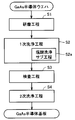
本発明にかかるGaAs半導体基板の製造方法の一実施形態は、図2を参照して、実施形態1のGaAs半導体基板の製造方法であって、GaAs半導体ウエハを研磨する研磨工程S1と、研磨されたGaAs半導体ウエハを洗浄する1次洗浄工程S2と、1次洗浄後のGaAs半導体ウエハの厚さおよび主表面の粗さを検査する検査工程S3と、検査後のGaAs半導体ウエハを塩酸以外の酸およびアルカリのいずれかにより洗浄する2次洗浄工程S4とを備える。かかる製造方法によって、実施形態1のGaAs半導体基板を製造することが可能となる。
(Embodiment 2)
One embodiment of a method for producing a GaAs semiconductor substrate according to the present invention is a method for producing a GaAs semiconductor substrate according to
本実施形態のGaAs半導体基板は、図2を参照して、具体的には以下のようにして製造される。まず、GaAs半導体ウエハを準備する。GaAs半導体ウエハは、GaAs半導体結晶インゴットを(100)面に対して6〜16°の傾斜角を有する互いに平行な面でスライスして、その外周を研削して外形を整え、その表面部の加工変質層をエッチングにより除去することにより得られる。ここで、GaAs半導体結晶インゴットを成長させる方法には、特に制限はなく、HB(水平ブリッジマン)法、LEC(液体封止型チョクラルスキー)法、VB(垂直ブリッジマン)法などの各種方法によって成長させることができる。 The GaAs semiconductor substrate of the present embodiment is specifically manufactured as follows with reference to FIG. First, a GaAs semiconductor wafer is prepared. A GaAs semiconductor wafer is formed by slicing a GaAs semiconductor crystal ingot with parallel planes having an inclination angle of 6 to 16 ° with respect to the (100) plane, grinding the outer periphery thereof, adjusting the outer shape, and processing the surface portion. It is obtained by removing the altered layer by etching. Here, the method for growing the GaAs semiconductor crystal ingot is not particularly limited, and various methods such as an HB (horizontal Bridgman) method, an LEC (liquid sealed Czochralski) method, and a VB (vertical Bridgman) method. Can be grown by.
次に、上記のようにして得られたGaAs半導体ウエハを研磨する(研磨工程S1)。研磨工程には、1以上のサブ工程が含まれ得る。ウエハの研磨効率を高めるため、ラッピング、粗(ラフ)ポリシング、微細(ファイン)ポリシングの3つのサブ工程が含まれることが好ましい。ここで、ラッピングにおいては、平均粒径が2μm〜10μm程度の酸化セリウム砥粒または酸化アルミニウム砥粒が好ましく用いられる。また、粗ポリシングにおいては、コロイダルシリカと塩素系研磨剤との混合物が好ましく用いられる。また、微細ポリシングにおいては、塩素系研磨剤が好ましく用いられる。 Next, the GaAs semiconductor wafer obtained as described above is polished (polishing step S1). The polishing process can include one or more sub-processes. In order to increase the polishing efficiency of the wafer, it is preferable to include three sub-steps of lapping, rough (rough) polishing, and fine (fine) polishing. Here, in the lapping, cerium oxide abrasive grains or aluminum oxide abrasive grains having an average particle diameter of about 2 μm to 10 μm are preferably used. In rough polishing, a mixture of colloidal silica and a chlorine-based abrasive is preferably used. In the fine polishing, a chlorine-based abrasive is preferably used.
次に、研磨されたGaAs半導体ウエハを1次洗浄する(1次洗浄工程S2)。1次洗浄工程には、1以上のサブ洗浄工程が含まれ得る。ウエハの洗浄効率を高めるために、有機溶剤洗浄、酸およびアルカリのいずれかによる洗浄、純水洗浄などのサブ工程が含まれることが好ましい。また、洗浄剤を除去するために、1次洗浄工程の最終サブ工程として、純水洗浄が好ましく行なわれる。 Next, the polished GaAs semiconductor wafer is subjected to primary cleaning (primary cleaning step S2). The primary cleaning process may include one or more sub-cleaning processes. In order to increase the cleaning efficiency of the wafer, it is preferable to include sub-steps such as organic solvent cleaning, cleaning with one of acid and alkali, and pure water cleaning. In order to remove the cleaning agent, pure water cleaning is preferably performed as the final sub-step of the primary cleaning step.
ここで、GaAs半導体ウエハの主表面の粗さを低減する観点から、1次洗浄工程S2はGaAs半導体ウエハを塩酸で洗浄する塩酸洗浄サブ工程S2aを含むことが好ましい。しかし、塩酸洗浄サブ工程S2a後のGaAs半導体ウエハの主表面には5×1012cm-2程度の濃度の塩素原子が残存するため、そのサブ工程後のGaAs半導体ウエハを塩酸以外の酸およびアルカリのいずれかにより洗浄することが好ましい。 Here, from the viewpoint of reducing the roughness of the main surface of the GaAs semiconductor wafer, the primary cleaning step S2 preferably includes a hydrochloric acid cleaning sub-step S2a for cleaning the GaAs semiconductor wafer with hydrochloric acid. However, since chlorine atoms having a concentration of about 5 × 10 12 cm −2 remain on the main surface of the GaAs semiconductor wafer after the hydrochloric acid cleaning sub-step S2a, the GaAs semiconductor wafer after the sub-step is treated with acids and alkalis other than hydrochloric acid. It is preferable to wash by any of the above.
次いで、1次洗浄されたGaAs半導体ウエハを乾燥させる。かかる乾燥工程には、1以上のサブ工程が含まれ得る。ウエハの乾燥効率を高めるために、アルコール蒸気乾燥(たとえばイソプロピルアルコール蒸気乾燥)、スピン乾燥、マランゴニ乾燥、ロタゴニ乾燥などのサブ工程が含まれることが好ましい。 Next, the first cleaned GaAs semiconductor wafer is dried. Such a drying step can include one or more sub-steps. In order to increase the drying efficiency of the wafer, it is preferable to include sub-steps such as alcohol vapor drying (eg, isopropyl alcohol vapor drying), spin drying, Marangoni drying, and rotagoni drying.
次に、1次洗浄後のGaAs半導体ウエハの厚さおよび主表面の平坦度を検査する(検査工程S3)。ここで、主表面の平坦度とは、ウエハの厚さバラツキ(TTV:Total Thickness Variation)、そり(Warp)などウエハ全面に渡る平面の形状精度をいい、フィゾー干渉計などにより測定される。ウエハの厚さはウエハの機械的強度に関わる。また、ウエハの主表面の平坦度は、その主表面上に形成されるIII−V族化合物半導体層上にパターンを形成してIII−V族化合物半導体デバイスを製造する場合に、そのパターンの精度を左右する。したがって、半導体ウエハの厚さおよび主表面の平坦度は、III−V族化合物半導体デバイスの特性に関わる重要な検査項目である。 Next, the thickness of the GaAs semiconductor wafer after the primary cleaning and the flatness of the main surface are inspected (inspection step S3). Here, the flatness of the main surface refers to the shape accuracy of a plane over the entire surface of the wafer, such as wafer thickness variation (TTV) and warp, and is measured by a Fizeau interferometer or the like. The thickness of the wafer is related to the mechanical strength of the wafer. The flatness of the main surface of the wafer is determined by the accuracy of the pattern when a III-V compound semiconductor device is manufactured by forming a pattern on the III-V compound semiconductor layer formed on the main surface. Influences. Therefore, the thickness of the semiconductor wafer and the flatness of the main surface are important inspection items related to the characteristics of the III-V compound semiconductor device.
次に、検査後のGaAs半導体ウエハを塩酸以外の酸およびアルカリのいずれかにより洗浄する(2次洗浄工程S4)。上記の検査工程S3においても、ウエハの主表面に塩素原子が付着する場合があるからである。ウエハの主表面に存在する塩素原子は、Ga、In、As、Pまたは主表面上に存在するアンモニアなどのアルカリと反応して塩化物を形成する。かかる塩化物は、塩酸以外の酸およびアルカリのいずれかによる洗浄により容易に除去される。塩酸以外の酸およびアルカリのいずれかにより洗浄されたGaAs半導体ウエハは、その後、純水洗浄され、次いで乾燥される。ここで、乾燥方法は、1次洗浄後の乾燥と同様の方法が行なわれる。 Next, the inspected GaAs semiconductor wafer is cleaned with either acid or alkali other than hydrochloric acid (secondary cleaning step S4). This is because chlorine atoms may adhere to the main surface of the wafer also in the inspection step S3. Chlorine atoms present on the main surface of the wafer react with Ga, In, As, P, or alkali such as ammonia present on the main surface to form chloride. Such chloride is easily removed by washing with either an acid other than hydrochloric acid or an alkali. The GaAs semiconductor wafer cleaned with either acid or alkali other than hydrochloric acid is then cleaned with pure water and then dried. Here, the drying method is the same as the drying after the primary cleaning.
次に、2次洗浄されたGaAs半導体ウエハ(これをGaAs半導体基板いう)を、必要最小限の表面検査を行なった後、PP(ポリプロピレン)、PC(ポリカーボネート)、PBT(ポリブチルテレフタレート)などの材質で形成された容器に入れ、その容器を酸素バリア性の高いアルミニウム箔をラミネートしたPE(ポリエチレン)などの材質で形成された袋に入れて、その袋内を665Pa(5Torr)以下の真空とした後、窒素ガスを入れて、その袋をシールすることにより、ウエハを窒素ガス雰囲気内に封入する。 Next, after the secondary cleaned GaAs semiconductor wafer (referred to as a GaAs semiconductor substrate) is subjected to the minimum surface inspection, PP (polypropylene), PC (polycarbonate), PBT (polybutyl terephthalate), etc. Put the container in a container made of a material, put the container in a bag made of a material such as PE (polyethylene) laminated with aluminum foil having a high oxygen barrier property, and evacuate the bag with a vacuum of 665 Pa (5 Torr) or less. After that, nitrogen gas is introduced and the bag is sealed to enclose the wafer in a nitrogen gas atmosphere.
または、上記表面検査後のGaAs半導体基板を入れた上記容器を酸素透過度が0.5ml・m-2・day-1・atm-1以上の第1の樹脂袋に入れて、第1の樹脂袋をシール(1次シール)する。次いで、1次シールされた第1の樹脂袋を、脱酸素剤とともに、酸素透過度が0.5ml・m-2・day-1・atm-1未満の第2の樹脂袋に入れて、第2の樹脂袋をシールする。ここで、脱酸素剤として脱水作用をも有するもの(たとえば、鉄粉末、二酸化チタン粉末など)を用いることにより、上記容器内部の水分も低減することができる。 Alternatively, the container containing the GaAs semiconductor substrate after the surface inspection is put in a first resin bag having an oxygen permeability of 0.5 ml · m −2 · day −1 · atm −1 or more, and the first resin Seal the bag (primary seal). Next, the first sealed first resin bag is put together with an oxygen scavenger into a second resin bag having an oxygen permeability of less than 0.5 ml · m −2 · day −1 · atm −1 , 2 resin bags are sealed. Here, by using an oxygen scavenger that also has a dehydrating action (for example, iron powder, titanium dioxide powder, etc.), the moisture inside the container can also be reduced.
ここで、図3を参照して、本実施形態のGaAs半導体基板の製造方法において、1次洗浄工程、検査工程および2次洗浄工程はクリーン室1内で行われ、クリーン室1内では、室外から純水の霧2w中を通過して空気が導入され、導入された空気は活性炭を含んだフィルタ4fを通過して循環されることが好ましい。クリーン室1内の空気が循環の際にフィルタ4fを通過することに加えて、室外の空気がクリーン室1内に導入される際に純水の霧2w中を通過することにより、クリーン室1内の塩素原子含有濃度を効率よく低減し、低く維持することができる。このクリーン室内で、GaAs半導体ウエハの1次洗浄工程、検査工程および2次洗浄工程を行なうことにより、2次洗浄工程後のGaAs半導体基板の主表面における塩素原子濃度を低く維持することができる。
Here, referring to FIG. 3, in the method of manufacturing a GaAs semiconductor substrate of the present embodiment, the primary cleaning step, the inspection step, and the secondary cleaning step are performed in the
図3を参照して、室外からクリーン室内への空気の導入は、たとえば以下のようにして行なわれる。ここで、図3の矢印は空気ライン6における空気の流れを示す。まず、室外の空気は空気ライン6aを通して純水スクラバ室2内に導入される。純水スクラバ室2内では純水の霧2wが形成されており、空気は純水の霧2w中を通過することにより、空気中の塩素原子含有濃度が低減される。純水の霧2w中を通過した空気は、空気ライン6bを通して除湿室3に導入され、空気中の湿度が低減される。除湿室3内を通過した空気は、空気ライン6cを通してフィルタ室4に導入される。フィルタ室4には活性炭を含んだフィルタ4fが配置されており、空気は活性炭を含んだフィルタ4fを通過することにより、空気中の塩素原子含有濃度がさらに低減される。こうして、空気は活性炭を含んだフィルタ4fを通過した塩素原子含有濃度が極めて低減した空気が、空気ライン6dを通してクリーン室1内に導入される。
Referring to FIG. 3, the introduction of air from the outside into the clean room is performed, for example, as follows. Here, the arrows in FIG. 3 indicate the flow of air in the
また、クリーン室内の空気の循環は、たとえば空気ライン6eに設置された空気循環装置7により、以下のようにして行なわれる。クリーン室1内の空気は、負圧バッファ室5を経由して空気ライン6eおよび6fを通してフィルタ室4内に流れる。空気はフィルタ4室内の活性炭を含んだフィルタ4fを通過することにより、クリーン室1の微小な隙間などからクリーン室1内に侵入した塩素原子、室内で発生した塩素原子などが効率的に除去され、空気中の塩素原子含有濃度がさらに低減され低く維持される。この塩素原子含有濃度がさらに低減され低く維持された空気が、空気ライン6dを通してクリーン室1内に戻る。ここで、空気循環装置7としては、循環ファン、循環ポンプなどが用いられる。
Further, the circulation of the air in the clean room is performed, for example, by the air circulation device 7 installed in the
このようにして、塩素原子含有濃度が低減かつ維持されたクリーン室1が得られ、かかるクリーン室1内でGaAs半導体ウエハの1次洗浄工程、検査工程および2次洗浄工程を行なうことにより、主表面における塩素原子濃度が低減したGaAs半導体基板が得られる。ここで、主表面における塩素原子濃度が1×1013cm-2以下のGaAs半導体基板を得る観点から、2次洗浄後におけるクリーン室内の塩素原子含有濃度は、1500ng・m-3以下であることが好ましい。また、主表面における塩素原子濃度が3×1012cm-2以下のGaAs半導体基板を得る観点から、2次洗浄後におけるクリーン室内の塩素原子含有濃度は、400ng・m-3以下であることがより好ましい。
In this way, a
(実施形態3)
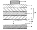
本発明にかかるIII−V族化合物半導体デバイスの一実施形態は、図4を参照して、主表面10mが(100)面10aに対して6〜16°の傾斜角θを有し主表面10mにおける塩素原子濃度が1×1013cm-2以下であるGaAs半導体基板10と、GaAs半導体基板10の主表面10m上に形成されている少なくとも1層の3種類以上の元素を含むIII−V族化合物半導体層20と、を備える。かかる半導体デバイスは、GaAs半導体基板の主表面における塩素原子濃度が1×1013cm-2以下であるため、III−V族化合物半導体層への塩素原子の取り込みが少なく、半導体デバイスの特性が高くなる。
(Embodiment 3)
Referring to FIG. 4, one embodiment of a III-V group compound semiconductor device according to the present invention has a
本実施形態のIII−V族化合物半導体デバイスは、たとえば、図4を参照して、GaAs半導体基板10であるn型GaAs半導体基板と、GaAs半導体基板10の主表面10m上に形成されている少なくとも1層の3種類以上の元素を含むIII−V族化合物半導体層20としてn型Alx1Gay1In1-x1-y1P(0<x1、0<y1、x1+y1<1)半導体層21、5対の井戸層(Gay3In1-y3P(0<y3<1)層)と障壁層(Alx4Gay4In1-x4-y4P(0<x4、0<y4、x4+y4<1)層)で形成される多重量子井戸構造の発光層22およびp型Alx2Gay2In1-x2-y2P(0<x2、0<y2、x2+y2<1)半導体層23とを備えるLEDである。
For example, referring to FIG. 4, the III-V group compound semiconductor device of the present embodiment includes at least an n-type GaAs semiconductor substrate which is a
また、本実施形態のLEDは、3種類以上の元素を含むIII−V族化合物半導体層20の最上層であるp型Alx2Gay2In1-x2-y2P(0<x2、0<y2、x2+y2<1)半導体層23上にp型GaAsコンタクト層25が形成され、このp型GaAsコンタクト層25上にp側電極30としてAu−Zn電極を備え、n型GaAs半導体基板(GaAs半導体基板10)のIII−V族化合物半導体層20が形成されていない主表面上にn側電極40としてAu−Ge電極を備える。
In addition, the LED of this embodiment is p-type Al x2 Ga y2 In 1-x2-y2 P (0 < x2, 0 < y2), which is the uppermost layer of the III-V
本実施形態のLEDは、GaAs半導体基板10の主表面10mにおける塩素原子濃度が1×1013cm-2以下であるため、III−V族化合物半導体層20への塩素原子の取り込みが少ないため、発光層22からの発光が阻害されないため、高い発光強度が得られる。
In the LED of this embodiment, since the chlorine atom concentration on the
(実施形態4)
本発明にかかるIII−V族化合物半導体デバイスの製造方法の一実施形態は、図4を参照して、実施形態3のIII−V族化合物半導体デバイスの製造方法であって、GaAs半導体基板10を準備する工程と、GaAs半導体基板10の主表面10m上に少なくとも1層の3種類以上の元素を含むIII−V族化合物半導体層20を成長させる工程とを備える。かかる製造方法により、高い特性を有するIII−V族化合物半導体デバイスが容易に得られる。
(Embodiment 4)
An embodiment of a method for manufacturing a group III-V compound semiconductor device according to the present invention is a method for manufacturing a group III-V compound semiconductor device according to the third embodiment with reference to FIG. A step of preparing, and a step of growing a group III-V
ここで、GaAs半導体基板10を準備する工程において、たとえば、実施形態2の製造方法により得られるGaAs半導体基板を準備することができる。
Here, in the step of preparing the
また、図4を参照して、GaAs半導体基板10の主表面10m上に少なくとも1層の3種類以上の元素を含むIII−V族化合物半導体層20を成長させる工程において、たとえば、GaAs半導体基板10であるn型GaAs半導体基板の主表面上に、MOVPE(有機金属気相成長)法により、少なくとも1層の3種類以上の元素を含むIII−V族化合物半導体層20として、n型Alx1Gay1In1-x1-y11P(0<x1、0<y1、x1+y1<1)半導体層21、5対の井戸層(Gay3In1-y3P(0<y3<1)層)と障壁層(Alx4Gay4In1-x4-y4P(0<x4、0<y4、x4+y4<1)層)で形成される多重量子井戸構造の発光層22およびp型Alx2Gay2In1-x2-y2P(0<x2、0<y2、x2+y2<1)半導体層23を順次成長させる。
Referring to FIG. 4, in the step of growing group III-V
次に、III−V族化合物半導体層20の最上層であるp型Alx2Gay2In1-x2-y2P(0<x2、0<y2、x2+y2<1)半導体層23上に、MOVPE(有機金属気相成長)法により、p型GaAsコンタクト層25を成長させる。
Next, on the p-type Al x2 Ga y2 In 1 -x2 -y2 P (0 <x2, 0 <y2, x2 + y2 <1)
次に、p型GaAsコンタクト層25上に、真空蒸着法により、p側電極30としてAu−Zn電極を形成し、n型GaAs半導体基板(GaAs半導体基板10)のIII−V族化合物半導体層20が形成されていない主表面上に、真空蒸着法により、n側電極40としてAu−Ge電極を形成する。
Next, an Au—Zn electrode is formed as the p-
(実施例1)
1.GaAs半導体ウエハの準備
縦型ボート(垂直ブリッジマン)法により成長させたGaAs半導体インゴットを、(100)面から[011]方向に15°傾いた面に平行にワイヤーソーでスライスして、GaAs半導体ウエハを得た。このGaAs半導体ウエハの主表面は、(100)面から[011]方向に15°傾いた面に対して0.1°以下の面である。このGaAs半導体ウエハの外周部分をダイヤモンド砥石で研削し、外形を整えた。外形を整えたGaAs半導体ウエハの加工変質層を除去するため、その主表面をアンモニアおよび過酸化水素を含む水溶液(アンモニア濃度4質量%、過酸化水素濃度4質量%)でエッチングした。
Example 1
1. Preparation of GaAs semiconductor wafer A GaAs semiconductor ingot grown by the vertical boat (vertical Bridgman) method is sliced with a wire saw parallel to a plane inclined by 15 ° in the [011] direction from the (100) plane, and the GaAs semiconductor A wafer was obtained. The main surface of the GaAs semiconductor wafer is a surface of 0.1 ° or less with respect to a surface inclined by 15 ° in the [011] direction from the (100) surface. The outer periphery of the GaAs semiconductor wafer was ground with a diamond grindstone to adjust the outer shape. In order to remove the work-affected layer of the GaAs semiconductor wafer having a trimmed outer shape, the main surface was etched with an aqueous solution containing ammonia and hydrogen peroxide (
2.研磨工程(S1)
GaAs半導体ウエハの研磨する主表面と反対側の主表面(主裏面)にワックスを塗布して加熱したセラミック板に接着した。このセラミック板を冷却した後、以下の手順でGaAs半導体ウエハの主表面のラッピング、粗ポリッシュ、微細ポリッシュを実施した。まず、平均粒径が6μmのSiC砥粒あるいは酸化アルミニウム砥粒を用いて、ラッピングを実施した。次いで、平均粒径0.03μmのコロイダルシリカと塩素系研磨剤(フジミインコーポレーテッド社製INSEC NIB)の混合物を用いて、粗ポリシングを実施した。次いで、塩素系研磨剤(フジミ研磨剤社製INSEC NIB)を用いて、微細ポリッシュを実施した。
2. Polishing process (S1)
Wax was applied to the main surface (main back surface) opposite to the main surface to be polished of the GaAs semiconductor wafer and bonded to a heated ceramic plate. After cooling the ceramic plate, lapping, rough polishing, and fine polishing of the main surface of the GaAs semiconductor wafer were performed in the following procedure. First, lapping was performed using SiC abrasive grains or aluminum oxide abrasive grains having an average grain diameter of 6 μm. Next, rough polishing was performed using a mixture of colloidal silica having an average particle size of 0.03 μm and a chlorine-based abrasive (INSEC NIB manufactured by Fujimi Incorporated). Next, fine polishing was performed using a chlorine-based abrasive (INSEC NIB manufactured by Fujimi Abrasive Co., Ltd.).
3.1次洗浄工程(S2)
上記研磨後に、GaAS半導体ウエハを超純水(本願においては、比抵抗10MΩ・cm以上に精製された純水をいう。以下同じ。)で洗浄して、ウエハをセラミックス板から分離した。次に、上記研磨後のGaAs半導体ウエハを、クリーン室内に移動して、クリーン室内において以下の有機溶剤洗浄、酸およびアルカリのいずれかによる洗浄、純水洗浄を実施した。まず、ウエハの主裏面のワックスをイソプロピルアルコールで有機溶剤洗浄を実施した。次いで、1質量%の塩酸および0.5質量%のTMAH(テトラメチルアンモニウムハイドロオキシド)のいずれかによる洗浄を実施した。次いで、超純水で純水洗浄した。次いで、クリーン室内で、1次洗浄後のGaAs半導体ウエハをイソプロピルアルコールでアルコール蒸気乾燥を行なった。
3. Primary cleaning process (S2)
After the polishing, the GaAS semiconductor wafer was washed with ultrapure water (in this application, pure water purified to a specific resistance of 10 MΩ · cm or more; the same applies hereinafter) to separate the wafer from the ceramic plate. Next, the polished GaAs semiconductor wafer was moved into a clean chamber, and the following organic solvent cleaning, cleaning with one of acid and alkali, and pure water cleaning were performed in the clean chamber. First, the wax on the main back surface of the wafer was cleaned with an organic solvent with isopropyl alcohol. Next, washing with either 1% by mass hydrochloric acid or 0.5% by mass TMAH (tetramethylammonium hydroxide) was performed. Next, pure water was washed with ultrapure water. Subsequently, the GaAs semiconductor wafer after the primary cleaning was dried with alcohol vapor with isopropyl alcohol in a clean room.
4.検査工程(S3)
次に、クリーン室内で、乾燥後のGaAs半導体ウエハの厚さおよび主表面の粗さを検査した。検査方法には、特に制限はないが、ウエハの厚さは非接触厚さ計などにより検査し、主表面の平坦度はフィゾー干渉計などにより検査した。
4). Inspection process (S3)
Next, the thickness of the dried GaAs semiconductor wafer and the roughness of the main surface were inspected in a clean room. There are no particular restrictions on the inspection method, but the wafer thickness was inspected with a non-contact thickness meter, etc., and the flatness of the main surface was inspected with a Fizeau interferometer.
5.2次洗浄工程(S4)
次に、クリーン室内で、検査後のGaAs半導体ウエハについて、以下の手順で塩酸以外の酸およびアルカリのいずれかによる洗浄、純水洗浄を実施した。まず、1質量%の硝酸および0.5質量%のアンモニアのいずれかによる洗浄を実施した。次いで、超純水で純水洗浄を実施した。次いで、2次洗浄後のGaAs半導体ウエハをイソプロピルアルコールでアルコール蒸気乾燥を実施した。
5. Secondary cleaning step (S4)
Next, in the clean room, the GaAs semiconductor wafer after the inspection was cleaned with either acid or alkali other than hydrochloric acid and pure water according to the following procedure. First, cleaning with either 1% by mass of nitric acid or 0.5% by mass of ammonia was performed. Next, pure water cleaning was performed with ultrapure water. Next, the GaAs semiconductor wafer after the secondary cleaning was subjected to alcohol vapor drying with isopropyl alcohol.
図3を参照して、上記1次洗浄工程、検査工程および2次洗浄工程が行なわれるクリーン室1は、室外から純水の霧2w中を通過して空気が導入され、導入された空気は活性炭を含んだフィルタ4fを通過して循環させた。このため、クリーン室内の塩素原子含有濃度は低く維持されており、上記2次洗浄後のクリーン室内の塩素原子含有濃度は120ng・cm-3であった。
Referring to FIG. 3, in the
上記の工程を経た後のGaAs半導体ウエハ(すなわちGaAs半導体基板)を、表面検査をして、クリーン室内に2時間置いた。このときのGaAs半導体基板の主表面における塩素原子濃度は、TXRFにより測定したところ、167×1010cm-2であった。結果を表1にまとめた。 The GaAs semiconductor wafer (that is, the GaAs semiconductor substrate) after the above steps was subjected to surface inspection and placed in a clean room for 2 hours. The chlorine atom concentration on the main surface of the GaAs semiconductor substrate at this time was 167 × 10 10 cm −2 as measured by TXRF. The results are summarized in Table 1.
6.AlxGayIn1-x-yP(0≦x、0≦y、x+y≦1)エピタキシャル層の成長
次に、図GaAs半導体基板の主表面上に、少なくとも1層の3種類以上の元素を含むIII−V族化合物半導体層20として、OMVPE(有機金属気相成長)法により、厚さ1μmのn型Alx1Gay1In1-x1-y1P(x1=0.25、y1=0.25)半導体層21、5対の厚さ10nmの井戸層(Gay3In1-y3P(y3=0.5)半導体層)と厚さ10nmの障壁層(Alx4Gay4In1-x4-y4P(x4=0.25、y4=0.25)半導体層)で形成される多重量子井戸構造の発光層22およびp型Gay3In1-y3P(y3=0.5)半導体層23を順にエピタキシャル成長させた。こうして得られる複数のエピタキシャル成長層をAlGaInPエピタキシャル層と呼ぶ。
6). Growth of epitaxial layer of Al x Ga y In 1-xy P (0 ≦ x, 0 ≦ y, x + y ≦ 1) Next, at least one layer of three or more elements is included on the main surface of the GaAs semiconductor substrate. As the group III-V
こうして得られたAlGaInPエピタキシャル層のPL(フォトルミネッセンス)強度を以下のようにして測定した。励起光としてArレーザをAlGaInPエピタキシャル層に照射して、AlGaInPエピタキシャル層から放出されるPL光として波長が600nm以上700nm以下の範囲の光を分光して、フォトマルで検出してPL強度を算出した。本実施例におけるAlGaInPエピタキシャル層のPL強度は、70AU(任意単位)であった。結果を表1にまとめた。 The PL (photoluminescence) intensity of the AlGaInP epitaxial layer thus obtained was measured as follows. Ar laser was irradiated to the AlGaInP epitaxial layer as excitation light, and PL light emitted from the AlGaInP epitaxial layer was subjected to spectroscopy of light having a wavelength in the range of 600 nm to 700 nm and detected by photomultiplier to calculate the PL intensity. . The PL intensity of the AlGaInP epitaxial layer in this example was 70 AU (arbitrary unit). The results are summarized in Table 1.
(実施例2)
2次洗浄後のクリーン室内の塩素原子含有濃度Xが750ng・cm-3であること以外は、実施例1と同様にして、GaAs半導体ウエハについて、研磨工程、1次洗浄工程、検査工程および2次洗浄工程を実施してGaAs半導体基板を得た。本実施例で得られたGaAs半導体基板の主表面における塩素原子濃度Yは、668×1010cm-2であった。次に、実施例1と同様にして、このGaAs半導体基板の主表面上にAlGaInPエピタキシャル層を形成した。本実施例におけるAlGaInPエピタキシャル層のPL強度Zは、64AUであった。結果を表1にまとめた。
(Example 2)
Except that the chlorine atom containing concentration X in the clean chamber after the secondary cleaning is 750 ng · cm −3 , the polishing process, the primary cleaning process, the inspection process, and 2 are performed on the GaAs semiconductor wafer in the same manner as in Example 1. A next cleaning step was performed to obtain a GaAs semiconductor substrate. The chlorine atom concentration Y on the main surface of the GaAs semiconductor substrate obtained in this example was 668 × 10 10 cm −2 . Next, in the same manner as in Example 1, an AlGaInP epitaxial layer was formed on the main surface of the GaAs semiconductor substrate. The PL intensity Z of the AlGaInP epitaxial layer in this example was 64 AU. The results are summarized in Table 1.
(比較例1)
1次洗浄工程、検査工程および2次洗浄工程を上記クリーン室で行なうことなく、2次洗浄後の基板の周りの雰囲気塩素原子濃度Xが1514ng・cm-3であること以外は、実施例1と同様にして、GaAs半導体ウエハについて、研磨工程、1次洗浄工程、検査工程および2次洗浄工程を実施してGaAs半導体基板を得た。本比較例で得られたGaAs半導体基板の主表面における塩素原子濃度Yは、1302×1010cm-2であった。次に、実施例1と同様にして、このGaAs半導体基板の主表面上にAlGaInPエピタキシャル層を形成した。本比較例におけるAlGaInPエピタキシャル層のPL強度Zは、60AUであった。結果を表1にまとめた。
(Comparative Example 1)
Example 1 except that the ambient chlorine atom concentration X around the substrate after the secondary cleaning is 1514 ng · cm −3 without performing the primary cleaning step, the inspection step and the secondary cleaning step in the clean room. In the same manner as described above, a polishing process, a primary cleaning process, an inspection process, and a secondary cleaning process were performed on the GaAs semiconductor wafer to obtain a GaAs semiconductor substrate. The chlorine atom concentration Y on the main surface of the GaAs semiconductor substrate obtained in this comparative example was 1302 × 10 10 cm −2 . Next, in the same manner as in Example 1, an AlGaInP epitaxial layer was formed on the main surface of the GaAs semiconductor substrate. The PL intensity Z of the AlGaInP epitaxial layer in this comparative example was 60 AU. The results are summarized in Table 1.
(比較例2)
2次洗浄後の基板の周りの雰囲気塩素原子濃度Xが5387ng・cm-3であること以外は、比較例1と同様にして、GaAs半導体ウエハについて、研磨工程、1次洗浄工程、検査工程および2次洗浄工程を実施してGaAs半導体基板を得た。本比較例で得られたGaAs半導体基板の主表面における塩素原子濃度Yは、2299×1010cm-2であった。次に、実施例1と同様にして、このGaAs半導体基板の主表面上にAlGaInPエピタキシャル層を形成した。本比較例におけるAlGaInPエピタキシャル層のPL強度Zは、53AUであった。
(Comparative Example 2)
A GaAs semiconductor wafer is subjected to a polishing process, a primary cleaning process, an inspection process, and the like in the same manner as in Comparative Example 1 except that the atmospheric chlorine atom concentration X around the substrate after the secondary cleaning is 5387 ng · cm −3. A secondary cleaning process was performed to obtain a GaAs semiconductor substrate. The chlorine atom concentration Y on the main surface of the GaAs semiconductor substrate obtained in this comparative example was 2299 × 10 10 cm −2 . Next, in the same manner as in Example 1, an AlGaInP epitaxial layer was formed on the main surface of the GaAs semiconductor substrate. The PL intensity Z of the AlGaInP epitaxial layer in this comparative example was 53 AU.
(比較例3)
2次洗浄後の基板の周りの雰囲気塩素原子濃度Xが2471ng・cm-3であること以外は、比較例1と同様にして、GaAs半導体ウエハについて、研磨工程、1次洗浄工程、検査工程および2次洗浄工程を実施してGaAs半導体基板を得た。本比較例で得られたGaAs半導体基板の主表面における塩素原子濃度Yは、2413×1010cm-2であった。次に、実施例1と同様にして、このGaAs半導体基板の主表面上にAlGaInPエピタキシャル層を形成した。本比較例におけるAlGaInPエピタキシャル層のPL強度Zは、51AUであった。
(Comparative Example 3)
A GaAs semiconductor wafer is subjected to a polishing process, a primary cleaning process, an inspection process, and the like in the same manner as in Comparative Example 1 except that the atmospheric chlorine atom concentration X around the substrate after the secondary cleaning is 2471 ng · cm −3. A secondary cleaning process was performed to obtain a GaAs semiconductor substrate. The chlorine atom concentration Y on the main surface of the GaAs semiconductor substrate obtained in this comparative example was 2413 × 10 10 cm −2 . Next, in the same manner as in Example 1, an AlGaInP epitaxial layer was formed on the main surface of the GaAs semiconductor substrate. The PL intensity Z of the AlGaInP epitaxial layer in this comparative example was 51 AU.
(比較例4)
2次洗浄後の基板の周りの雰囲気塩素原子濃度Xが5700ng・cm-3であること以外は、比較例1と同様にして、GaAs半導体ウエハについて、研磨工程、1次洗浄工程、検査工程および2次洗浄工程を実施してGaAs半導体基板を得た。本比較例で得られたGaAs半導体基板の主表面における塩素原子濃度Yは、4421×1010cm-2であった。次に、実施例1と同様にして、このGaAs半導体基板の主表面上にAlGaInPエピタキシャル層を形成した。本比較例におけるAlGaInPエピタキシャル層のPL強度Zは、38AUであった。
(Comparative Example 4)
Except that the ambient chlorine atom concentration X around the substrate after the secondary cleaning is 5700 ng · cm −3 , the polishing process, the primary cleaning process, the inspection process, and the A secondary cleaning process was performed to obtain a GaAs semiconductor substrate. The chlorine atom concentration Y on the main surface of the GaAs semiconductor substrate obtained in this comparative example was 4421 × 10 10 cm −2 . Next, in the same manner as in Example 1, an AlGaInP epitaxial layer was formed on the main surface of the GaAs semiconductor substrate. The PL intensity Z of the AlGaInP epitaxial layer in this comparative example was 38 AU.
(比較例5)
2次洗浄後の基板の周りの雰囲気塩素原子濃度Xが6800ng・cm-3であること以外は、比較例1と同様にして、GaAs半導体ウエハについて、研磨工程、1次洗浄工程、検査工程および2次洗浄工程を実施してGaAs半導体基板を得た。本比較例で得られたGaAs半導体基板の主表面における塩素原子濃度Yは、4895×1010cm-2であった。次に、実施例1と同様にして、このGaAs半導体基板の主表面上にAlGaInPエピタキシャル層を形成した。本比較例におけるAlGaInPエピタキシャル層のPL強度Zは、32AUであった。結果を表1にまとめた。
(Comparative Example 5)
Except that the ambient chlorine atom concentration X around the substrate after the secondary cleaning is 6800 ng · cm −3 , the polishing process, the primary cleaning process, the inspection process, and the A secondary cleaning process was performed to obtain a GaAs semiconductor substrate. The chlorine atom concentration Y on the main surface of the GaAs semiconductor substrate obtained in this comparative example was 4895 × 10 10 cm −2 . Next, in the same manner as in Example 1, an AlGaInP epitaxial layer was formed on the main surface of the GaAs semiconductor substrate. The PL intensity Z of the AlGaInP epitaxial layer in this comparative example was 32 AU. The results are summarized in Table 1.
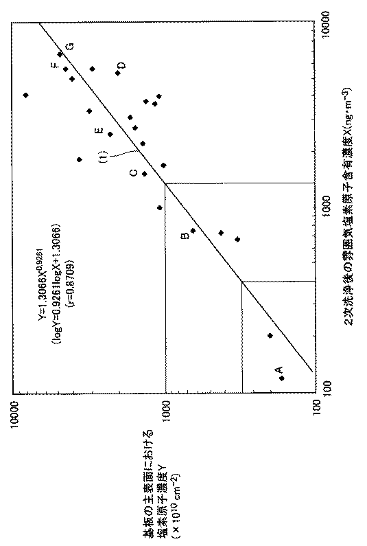
ここで、実施例1,2および比較例1〜5のそれぞれにおける2次洗浄後の基板の周りの雰囲気塩素原子含有濃度(実施例1,2においては、クリーン室内の塩素原子含有濃度X(単位:ng・m-3)と基板の主表面における塩素原子濃度Y(単位:×1010cm-2)との関係を、それぞれA点〜G点として、図6のグラフにプロットした。さらに、他の実施例および比較例における上記関係を図6のグラフにプロットした。 Here, in each of Examples 1 and 2 and Comparative Examples 1 to 5, the ambient chlorine atom-containing concentration around the substrate after the secondary cleaning (in Examples 1 and 2, the chlorine atom-containing concentration X (unit in the clean chamber) : Ng · m −3 ) and the chlorine atom concentration Y (unit: × 10 10 cm −2 ) on the main surface of the substrate, plotted as points A to G, respectively, in the graph of FIG. The above relationships in other examples and comparative examples are plotted in the graph of FIG.
図6から明らかなように、2次洗浄後の基板の周りの雰囲気塩素原子含有濃度X(単位:ng・m-3)と基板の主表面における塩素原子濃度Y(単位:×1010cm-2)との間には、相関係数r=0.8709の強さで、式(1)
Y=1.3066X0.9261 (1)
の相関関係が認められる。なお、両対数目盛りである図6において、(1)式は、logY=0.9261logX+1.3066と表わされる。
As apparent from FIG. 6, the ambient chlorine atom-containing concentration X (unit: ng · m −3 ) around the substrate after the secondary cleaning and the chlorine atom concentration Y (unit: × 10 10 cm − ) on the main surface of the substrate. 2 ) with a correlation coefficient r = 0.8709,
Y = 1.3066X 0.9261 (1)
The correlation is recognized. In FIG. 6, which is a logarithmic scale, the equation (1) is expressed as logY = 0.9261logX + 1.3066.
式(1)から、2次洗浄後のクリーン室内の塩素含有濃度Xを1500ng・m-3以下とすることにより主表面における塩素原子濃度Yが1×1013cm-2以下のGaAs半導体基板が得られ、2次洗浄後のクリーン室内の塩素含有濃度Xを400ng・m-3以下とすることにより主表面における塩素原子濃度Yが3×1012cm-2以下のGaAs半導体基板が得られることがわかる。 From formula (1), the chlorine content concentration X in the clean chamber after the secondary cleaning is set to 1500 ng · m −3 or less, whereby a GaAs semiconductor substrate having a chlorine atom concentration Y on the main surface of 1 × 10 13 cm −2 or less is obtained. A GaAs semiconductor substrate having a chlorine atom concentration Y on the main surface of 3 × 10 12 cm −2 or less can be obtained by setting the chlorine content concentration X in the clean chamber after the secondary cleaning to 400 ng · m −3 or less. I understand.
また、実施例1,2および比較例1〜5のそれぞれにおける基板の主表面における塩素原子濃度Y(単位:×1010cm-2)とその基板の主表面上に形成したAlGaInNエピタキシャル層のPL強度Z(単位:AU(任意単位))との関係を、それぞれA点〜G点として、図7のグラフにプロットした。 Further, the chlorine atom concentration Y (unit: × 10 10 cm −2 ) on the main surface of the substrate in each of Examples 1 and 2 and Comparative Examples 1 to 5 and the PL of the AlGaInN epitaxial layer formed on the main surface of the substrate The relationship with intensity Z (unit: AU (arbitrary unit)) was plotted in the graph of FIG.
図7から明らかなように、基板の主表面における塩素原子濃度Y(単位:×1010cm-2)と基板の主表面上に形成されたAlGaInPエピタキシャル層のPL強度Z(単位:AU)との間には、相関係数r=0.9972の強さで、式(2)
Z=−0.0075Y+69.792 (2)
の相関関係が認められる。
As is clear from FIG. 7, the chlorine atom concentration Y (unit: × 10 10 cm −2 ) on the main surface of the substrate and the PL intensity Z (unit: AU) of the AlGaInP epitaxial layer formed on the main surface of the substrate In the meantime, the correlation coefficient r = 0.9972 is strong, and the equation (2)
Z = −0.0075Y + 69.792 (2)
The correlation is recognized.
式(2)から、主表面における塩素原子濃度Yが1×1013cm-2以下のGaAs半導体基板の主表面上に62AU以上の高いPL強度を有するAlGaInPエピタキシャル層が形成され、主表面における塩素原子濃度Yが3×1012cm-2以下のGaAs半導体基板の主表面上に69AU以上のさらに高いPL強度を有するAlGaInPエピタキシャル層が形成されることがわかる。ここで、PL強度が高いAlGaInPエピタキシャル層を有する半導体デバイスほど発光が強く閾値が下がり高性能となる。 From formula (2), an AlGaInP epitaxial layer having a high PL intensity of 62 AU or more is formed on the main surface of a GaAs semiconductor substrate having a chlorine atom concentration Y of 1 × 10 13 cm −2 or less on the main surface, and chlorine on the main surface It can be seen that an AlGaInP epitaxial layer having a higher PL intensity of 69 AU or more is formed on the main surface of the GaAs semiconductor substrate having an atomic concentration Y of 3 × 10 12 cm −2 or less. Here, a semiconductor device having an AlGaInP epitaxial layer having a high PL intensity emits light more strongly and has a lower threshold value, resulting in higher performance.
今回開示された実施の形態および実施例はすべての点で例示であって制限的なものではないと考えられるべきである。本発明の範囲は、上記した説明でなくて特許請求の範囲によって示され、特許請求の範囲と均等の意味および範囲内のすべての変更が含まれることが意図される。 It should be understood that the embodiments and examples disclosed herein are illustrative and non-restrictive in every respect. The scope of the present invention is defined by the terms of the claims, rather than the description above, and is intended to include any modifications within the scope and meaning equivalent to the terms of the claims.
1 クリーン室、2 純水スクラバ室、2w 純水の霧、3 除湿室、4 フィルタ室、4f フィルタ4、5 負圧バッファ室、5d ダンパー、6,6a,6b,6c,6d,6e,6f 空気ライン、7 空気循環装置、10 GaAs半導体基板、10a (100)面、10m 主表面、20 III−V族化合物半導体層、21 n型Alx1Gay1In1-x1-y1P半導体層、22 発光層、23 p型Alx2Gay2In1-x2-y2P半導体層、25 p型GaAsコンタクト層、30 p側電極、40 n側電極、S1 研磨工程、S2 1次洗浄工程、S3 検査工程、S4 2次洗浄工程。
1 clean room, 2 pure water scrubber room, 2w mist of pure water, 3 dehumidification room, 4 filter room, 4f
Claims (9)
GaAs半導体ウエハを研磨する研磨工程と、研磨された前記GaAs半導体ウエハを洗浄する1次洗浄工程と、1次洗浄後の前記GaAs半導体ウエハの厚さおよび主表面の粗さを検査する検査工程と、検査後の前記GaAs半導体ウエハを塩酸以外の酸およびアルカリのいずれかにより洗浄する2次洗浄工程と、を備えるGaAs半導体基板の製造方法。 A method for producing a GaAs semiconductor substrate according to claim 1 or 2, comprising:
A polishing step for polishing a GaAs semiconductor wafer, a primary cleaning step for cleaning the polished GaAs semiconductor wafer, and an inspection step for inspecting the thickness and main surface roughness of the GaAs semiconductor wafer after the primary cleaning; And a secondary cleaning step of cleaning the GaAs semiconductor wafer after inspection with one of acids and alkalis other than hydrochloric acid.
前記クリーン室内では、室外から純水の霧中を通過して空気が導入され、導入された前記空気は前記活性炭を含んだフィルタを通過して循環される請求項3または請求項4に記載のGaAs半導体基板の製造方法。 The primary cleaning process, the inspection process and the secondary cleaning process are performed in a clean room,
5. The GaAs according to claim 3, wherein in the clean room, air is introduced from outside the room through a mist of pure water, and the introduced air is circulated through the filter containing the activated carbon. A method for manufacturing a semiconductor substrate.
前記GaAs半導体基板を準備する工程と、前記GaAs半導体基板の前記主表面上に少なくとも1層の3種類以上の元素を含むIII−V族化合物半導体層を成長させる工程と、を備えるIII−V族化合物半導体デバイスの製造方法。 A method for producing a group III-V compound semiconductor device according to claim 8, comprising:
A step of preparing the GaAs semiconductor substrate, and a step of growing a group III-V compound semiconductor layer including at least one layer of three or more elements on the main surface of the GaAs semiconductor substrate. A method of manufacturing a compound semiconductor device.
Priority Applications (6)
| Application Number | Priority Date | Filing Date | Title |
|---|---|---|---|
| JP2007313286A JP2009137776A (en) | 2007-12-04 | 2007-12-04 | GaAs SEMICONDUCTOR SUBSTRATE AND ITS MANUFACTURING METHOD, AND GROUP III-V COMPOUND SEMICONDUCTOR DEVICE AND ITS MANUFACTURING METHOD |
| TW101100847A TWI634623B (en) | 2007-12-04 | 2008-11-27 | GaAs SEMICONDUCTOR SUBSTRATE AND METHOD OF MANUFACTURING THE SAME, AND GROUP III-V COMPOUND SEMICONDUCTOR DEVICE AND METHOD OF MANUFACTURING THE SAME |
| TW104117543A TWI634624B (en) | 2007-12-04 | 2008-11-27 | GaAs SEMICONDUCTOR SUBSTRATE AND METHOD OF MANUFACTURING THE SAME, AND GROUP III-V COMPOUND SEMICONDUCTOR DEVICE AND METHOD OF MANUFACTURING THE SAME |
| TW097146001A TW200940757A (en) | 2007-12-04 | 2008-11-27 | GaAs semiconductor substrate and method of manufacturing the same, and group III-V compound semiconductor device and method of manufacturing the same |
| US12/326,452 US8044493B2 (en) | 2007-12-04 | 2008-12-02 | GaAs semiconductor substrate for group III-V compound semiconductor device |
| CNA2008101788825A CN101452894A (en) | 2007-12-04 | 2008-12-04 | Gaas semiconductor substrate , group III-v compound semiconductor device and method of manufacturing the same |
Applications Claiming Priority (1)
| Application Number | Priority Date | Filing Date | Title |
|---|---|---|---|
| JP2007313286A JP2009137776A (en) | 2007-12-04 | 2007-12-04 | GaAs SEMICONDUCTOR SUBSTRATE AND ITS MANUFACTURING METHOD, AND GROUP III-V COMPOUND SEMICONDUCTOR DEVICE AND ITS MANUFACTURING METHOD |
Publications (1)
| Publication Number | Publication Date |
|---|---|
| JP2009137776A true JP2009137776A (en) | 2009-06-25 |
Family
ID=40674884
Family Applications (1)
| Application Number | Title | Priority Date | Filing Date |
|---|---|---|---|
| JP2007313286A Pending JP2009137776A (en) | 2007-12-04 | 2007-12-04 | GaAs SEMICONDUCTOR SUBSTRATE AND ITS MANUFACTURING METHOD, AND GROUP III-V COMPOUND SEMICONDUCTOR DEVICE AND ITS MANUFACTURING METHOD |
Country Status (4)
| Country | Link |
|---|---|
| US (1) | US8044493B2 (en) |
| JP (1) | JP2009137776A (en) |
| CN (1) | CN101452894A (en) |
| TW (3) | TW200940757A (en) |
Families Citing this family (8)
| Publication number | Priority date | Publication date | Assignee | Title |
|---|---|---|---|---|
| JP5365454B2 (en) * | 2009-09-30 | 2013-12-11 | 住友電気工業株式会社 | Group III nitride semiconductor substrate, epitaxial substrate, and semiconductor device |
| JP4513927B1 (en) | 2009-09-30 | 2010-07-28 | 住友電気工業株式会社 | Group III nitride semiconductor substrate, epitaxial substrate, and semiconductor device |
| DE102013002637A1 (en) | 2013-02-15 | 2014-08-21 | Freiberger Compound Materials Gmbh | A method of making a gallium arsenide substrate, gallium arsenide substrate and use thereof |
| JP6310263B2 (en) * | 2014-01-30 | 2018-04-11 | 株式会社ニューフレアテクノロジー | Inspection device |
| CN103847032B (en) * | 2014-03-20 | 2016-01-06 | 德清晶辉光电科技有限公司 | The production technology of the ultra-thin quartz wafer of a kind of major diameter |
| JP2017032457A (en) * | 2015-08-04 | 2017-02-09 | 株式会社ニューフレアテクノロジー | Pattern inspection device |
| US10964786B2 (en) * | 2017-05-26 | 2021-03-30 | Sumitomo Electric Industries, Ltd. | Group III-V compound semiconductor substrate and group III-V compound semiconductor substrate with epitaxial layer |
| CN111376169A (en) * | 2018-12-28 | 2020-07-07 | 安集微电子科技(上海)股份有限公司 | Method for cleaning polished wafer |
Citations (6)
| Publication number | Priority date | Publication date | Assignee | Title |
|---|---|---|---|---|
| JPH0738194A (en) * | 1993-07-20 | 1995-02-07 | Mitsubishi Electric Corp | Semiconductor laser and manufacture thereof |
| JPH09278595A (en) * | 1996-04-10 | 1997-10-28 | Sumitomo Electric Ind Ltd | Iii-v compound semiconductor wafer and its production |
| JPH1192297A (en) * | 1997-09-11 | 1999-04-06 | Nec Corp | Production of disordered crystal structure, production of semiconductor laser and production of semiconductor laser having window structure |
| JP2001196333A (en) * | 2000-01-11 | 2001-07-19 | Hitachi Cable Ltd | Semiconductor wafer with off-angle |
| JP2001223191A (en) * | 2000-02-10 | 2001-08-17 | Sumitomo Electric Ind Ltd | Iii-v family compound semiconductor wafer and its manufacturing method |
| JP2002293686A (en) * | 2001-04-03 | 2002-10-09 | Hitachi Cable Ltd | Method of growing compound semiconductor signal crystal and substrate cut out of the same |
Family Cites Families (5)
| Publication number | Priority date | Publication date | Assignee | Title |
|---|---|---|---|---|
| JP2905667B2 (en) * | 1992-12-17 | 1999-06-14 | シャープ株式会社 | Method for manufacturing II-VI compound semiconductor thin film and II-VI compound semiconductor device |
| JPH08130337A (en) * | 1994-09-09 | 1996-05-21 | Sanyo Electric Co Ltd | Magnetoresistive element and manufacture thereof |
| US6639926B1 (en) * | 1998-03-25 | 2003-10-28 | Mitsubishi Chemical Corporation | Semiconductor light-emitting device |
| JP4282173B2 (en) * | 1999-09-03 | 2009-06-17 | シャープ株式会社 | Nitrogen compound semiconductor light emitting device and method of manufacturing the same |
| KR100382481B1 (en) * | 2000-06-09 | 2003-05-01 | 엘지전자 주식회사 | White Light Emitting Diode and Fabricating Method for the same |
-
2007
- 2007-12-04 JP JP2007313286A patent/JP2009137776A/en active Pending
-
2008
- 2008-11-27 TW TW097146001A patent/TW200940757A/en unknown
- 2008-11-27 TW TW101100847A patent/TWI634623B/en active
- 2008-11-27 TW TW104117543A patent/TWI634624B/en active
- 2008-12-02 US US12/326,452 patent/US8044493B2/en active Active
- 2008-12-04 CN CNA2008101788825A patent/CN101452894A/en active Pending
Patent Citations (6)
| Publication number | Priority date | Publication date | Assignee | Title |
|---|---|---|---|---|
| JPH0738194A (en) * | 1993-07-20 | 1995-02-07 | Mitsubishi Electric Corp | Semiconductor laser and manufacture thereof |
| JPH09278595A (en) * | 1996-04-10 | 1997-10-28 | Sumitomo Electric Ind Ltd | Iii-v compound semiconductor wafer and its production |
| JPH1192297A (en) * | 1997-09-11 | 1999-04-06 | Nec Corp | Production of disordered crystal structure, production of semiconductor laser and production of semiconductor laser having window structure |
| JP2001196333A (en) * | 2000-01-11 | 2001-07-19 | Hitachi Cable Ltd | Semiconductor wafer with off-angle |
| JP2001223191A (en) * | 2000-02-10 | 2001-08-17 | Sumitomo Electric Ind Ltd | Iii-v family compound semiconductor wafer and its manufacturing method |
| JP2002293686A (en) * | 2001-04-03 | 2002-10-09 | Hitachi Cable Ltd | Method of growing compound semiconductor signal crystal and substrate cut out of the same |
Also Published As
| Publication number | Publication date |
|---|---|
| TWI634623B (en) | 2018-09-01 |
| CN101452894A (en) | 2009-06-10 |
| TW201533853A (en) | 2015-09-01 |
| US20090140390A1 (en) | 2009-06-04 |
| TW201220439A (en) | 2012-05-16 |
| TWI634624B (en) | 2018-09-01 |
| TW200940757A (en) | 2009-10-01 |
| US8044493B2 (en) | 2011-10-25 |
Similar Documents
| Publication | Publication Date | Title |
|---|---|---|
| TWI634624B (en) | GaAs SEMICONDUCTOR SUBSTRATE AND METHOD OF MANUFACTURING THE SAME, AND GROUP III-V COMPOUND SEMICONDUCTOR DEVICE AND METHOD OF MANUFACTURING THE SAME | |
| TWI412637B (en) | A substrate III nitride substrate, a substrate with an epitaxial layer, a manufacturing method of the same, and a method for manufacturing the semiconductor element | |
| TWI462165B (en) | Production method of indium phosphide substrate, manufacturing method of epitaxial wafer, indium phosphide substrate and epitaxial wafer | |
| JP5365454B2 (en) | Group III nitride semiconductor substrate, epitaxial substrate, and semiconductor device | |
| TWI487005B (en) | A group III nitride semiconductor substrate, an epitaxial substrate, and a semiconductor device | |
| TWI415288B (en) | Free standing substrate, method for manufacturing the same, and semiconductor light emitting element | |
| JP2006339605A (en) | Method of evaluating damage of compound semiconductor member, method of manufacturing compound semiconductor member, gallium nitride based compound semiconductor member and gallium nitride based compound semiconductor film | |
| JP2007103457A (en) | Polishing slurry, surface treatment method of group iii nitride crystal, group iii nitride crystal substrate, group iii nitride crystal substrate with epitaxial layer, semiconductor device and its fabrication process | |
| JP6721816B2 (en) | Nitride semiconductor template and UV LED | |
| US8283694B2 (en) | GaN substrate, epitaxial layer-provided substrate, methods of manufacturing the same, and method of manufacturing semiconductor device | |
| JP2009182341A (en) | PRESERVATION METHOD OF GaN SUBSTRATE, PRESERVED SUBSTRATE, SEMICONDUCTOR DEVICE, AND MANUFACTURING METHOD FOR THEM | |
| EP2204478A2 (en) | AlGaInN and AlN substrates and method for cleaning them | |
| WO2008023617A1 (en) | Semiconductor device manufacturing method | |
| JP2007335583A (en) | METHOD FOR PRESERVING GaN SUBSTRATE, PRESERVED SUBSTRATE, SEMICONDUCTOR DEVICE AND MANUFACTURING METHOD FOR SEMICONDUCTOR DEVICE | |
| JP7160815B2 (en) | Gallium nitride substrates, free-standing substrates and functional devices | |
| JP2010118668A (en) | Damage evaluation method of compound semiconductor element member, production method of compound semiconductor element member, gallium nitride based compound semiconductor member, and gallium nitride based compound semiconductor film | |
| JP2011071546A (en) | Method of manufacturing compound semiconductor wafer | |
| JP2009140965A (en) | Epitaxial wafer, and method of fabricating epitaxial wafer | |
| JP5648726B2 (en) | GaN substrate and manufacturing method thereof, epitaxial substrate, and semiconductor device | |
| EP2980862A1 (en) | Manufacturing method for semiconductor light-emitting element, and semiconductor light-emitting element |
Legal Events
| Date | Code | Title | Description |
|---|---|---|---|
| A131 | Notification of reasons for refusal |
Free format text: JAPANESE INTERMEDIATE CODE: A131 Effective date: 20100126 |
|
| A02 | Decision of refusal |
Free format text: JAPANESE INTERMEDIATE CODE: A02 Effective date: 20100601 |