JP2009104687A - Storage device and control circuit - Google Patents
Storage device and control circuit Download PDFInfo
- Publication number
- JP2009104687A JP2009104687A JP2007273674A JP2007273674A JP2009104687A JP 2009104687 A JP2009104687 A JP 2009104687A JP 2007273674 A JP2007273674 A JP 2007273674A JP 2007273674 A JP2007273674 A JP 2007273674A JP 2009104687 A JP2009104687 A JP 2009104687A
- Authority
- JP
- Japan
- Prior art keywords
- memory
- cache area
- write
- read
- unit
- Prior art date
- Legal status (The legal status is an assumption and is not a legal conclusion. Google has not performed a legal analysis and makes no representation as to the accuracy of the status listed.)
- Pending
Links
Images


Classifications
-
- G—PHYSICS
- G11—INFORMATION STORAGE
- G11B—INFORMATION STORAGE BASED ON RELATIVE MOVEMENT BETWEEN RECORD CARRIER AND TRANSDUCER
- G11B5/00—Recording by magnetisation or demagnetisation of a record carrier; Reproducing by magnetic means; Record carriers therefor
- G11B5/02—Recording, reproducing, or erasing methods; Read, write or erase circuits therefor
- G11B5/09—Digital recording
-
- G—PHYSICS
- G06—COMPUTING; CALCULATING OR COUNTING
- G06F—ELECTRIC DIGITAL DATA PROCESSING
- G06F12/00—Accessing, addressing or allocating within memory systems or architectures
- G06F12/02—Addressing or allocation; Relocation
- G06F12/08—Addressing or allocation; Relocation in hierarchically structured memory systems, e.g. virtual memory systems
- G06F12/0802—Addressing of a memory level in which the access to the desired data or data block requires associative addressing means, e.g. caches
- G06F12/0866—Addressing of a memory level in which the access to the desired data or data block requires associative addressing means, e.g. caches for peripheral storage systems, e.g. disk cache
- G06F12/0871—Allocation or management of cache space
-
- G—PHYSICS
- G06—COMPUTING; CALCULATING OR COUNTING
- G06F—ELECTRIC DIGITAL DATA PROCESSING
- G06F12/00—Accessing, addressing or allocating within memory systems or architectures
- G06F12/02—Addressing or allocation; Relocation
- G06F12/0223—User address space allocation, e.g. contiguous or non contiguous base addressing
- G06F12/023—Free address space management
- G06F12/0238—Memory management in non-volatile memory, e.g. resistive RAM or ferroelectric memory
- G06F12/0246—Memory management in non-volatile memory, e.g. resistive RAM or ferroelectric memory in block erasable memory, e.g. flash memory
-
- G—PHYSICS
- G06—COMPUTING; CALCULATING OR COUNTING
- G06F—ELECTRIC DIGITAL DATA PROCESSING
- G06F12/00—Accessing, addressing or allocating within memory systems or architectures
- G06F12/02—Addressing or allocation; Relocation
- G06F12/08—Addressing or allocation; Relocation in hierarchically structured memory systems, e.g. virtual memory systems
- G06F12/0802—Addressing of a memory level in which the access to the desired data or data block requires associative addressing means, e.g. caches
- G06F12/0804—Addressing of a memory level in which the access to the desired data or data block requires associative addressing means, e.g. caches with main memory updating
-
- G—PHYSICS
- G06—COMPUTING; CALCULATING OR COUNTING
- G06F—ELECTRIC DIGITAL DATA PROCESSING
- G06F2212/00—Indexing scheme relating to accessing, addressing or allocation within memory systems or architectures
- G06F2212/10—Providing a specific technical effect
- G06F2212/1032—Reliability improvement, data loss prevention, degraded operation etc
- G06F2212/1036—Life time enhancement
-
- G—PHYSICS
- G06—COMPUTING; CALCULATING OR COUNTING
- G06F—ELECTRIC DIGITAL DATA PROCESSING
- G06F2212/00—Indexing scheme relating to accessing, addressing or allocation within memory systems or architectures
- G06F2212/21—Employing a record carrier using a specific recording technology
- G06F2212/217—Hybrid disk, e.g. using both magnetic and solid state storage devices
-
- G—PHYSICS
- G06—COMPUTING; CALCULATING OR COUNTING
- G06F—ELECTRIC DIGITAL DATA PROCESSING
- G06F2212/00—Indexing scheme relating to accessing, addressing or allocation within memory systems or architectures
- G06F2212/22—Employing cache memory using specific memory technology
- G06F2212/222—Non-volatile memory
-
- G—PHYSICS
- G06—COMPUTING; CALCULATING OR COUNTING
- G06F—ELECTRIC DIGITAL DATA PROCESSING
- G06F2212/00—Indexing scheme relating to accessing, addressing or allocation within memory systems or architectures
- G06F2212/72—Details relating to flash memory management
- G06F2212/7211—Wear leveling
Landscapes
- Engineering & Computer Science (AREA)
- Theoretical Computer Science (AREA)
- Physics & Mathematics (AREA)
- General Engineering & Computer Science (AREA)
- General Physics & Mathematics (AREA)
- Memory System Of A Hierarchy Structure (AREA)
- Signal Processing For Digital Recording And Reproducing (AREA)
- Debugging And Monitoring (AREA)
- Memory System (AREA)
- Read Only Memory (AREA)
- Techniques For Improving Reliability Of Storages (AREA)
Abstract
Description
本発明は、記憶媒体としてディスク媒体と不揮発メモリを使用するハイブリッド型の記憶装置及び制御回路に関し、特に、キャッシュ領域としてフラッシュメモリなどの書き換え回数に制限を持つ不揮発メモリを使用する記憶装置及び制御回路に関する。
The present invention relates to a hybrid storage device and a control circuit that use a disk medium and a nonvolatile memory as a storage medium, and in particular, a storage device and a control circuit that use a nonvolatile memory having a limited number of rewrites such as a flash memory as a cache area. About.
従来、磁気ディスク装置にあっては、記憶媒体としてヘッドによりデータを記録して再生する磁気ディスクを使用しているが、これに加え不揮発メモリであるフラッシュメモリを組み合わせたハイブリッド型の磁気ディスク装置が実用化されている。 Conventionally, in a magnetic disk device, a magnetic disk that records and reproduces data by a head is used as a storage medium. In addition, a hybrid magnetic disk device that combines a flash memory that is a nonvolatile memory is used. It has been put into practical use.
バイブリッド型の磁気ディスク装置は、例えばホストからのライトコマンドにより受領したライトデータをフラッシュメモリに一時的に保存し、フラッシュメモリにライトデータが保持しきれなくなったときに、ディスク媒体上にデータを書き込むようにするライトキャッシュ機能を持つようにしている。 For example, a hybrid magnetic disk device temporarily stores write data received by a write command from a host in a flash memory, and stores data on a disk medium when the write data cannot be held in the flash memory. It has a write cache function that allows writing.
また、ホストからリードコマンドを受領した時は、その対象データがフラッシュメモリ内に存在する場合には、フラッシュメモリからデータを読出してホストに対して転送するリードキャッシュ機能を持つようにしている。 Further, when a read command is received from the host, if the target data exists in the flash memory, a read cache function for reading the data from the flash memory and transferring it to the host is provided.
このようにフラッシュメモリに対しデータを書き込んだり読み出したりしている間、磁気ディスクを回転させるスピンドルモータを停止させておくことが可能であり、これにより磁気ディスク装置の消費電力を抑えることができ、主にモバイル型のパーソナルコンピュータなどで有効となる。 Thus, while writing data to or reading data from the flash memory, it is possible to stop the spindle motor that rotates the magnetic disk, thereby reducing the power consumption of the magnetic disk device, Effective mainly for mobile personal computers.
一方、ハイブリッド型の磁気ディスク装置に不揮発メモリとして使用しているフラッシュメモリは、書き換え動作より素子劣化が進行する特徴があり、書き換えおよび消去回数に制限がある。現状では、約十万回程度までの書き換えが可能とされている。 On the other hand, a flash memory used as a non-volatile memory in a hybrid type magnetic disk device has a feature that element deterioration progresses more than a rewrite operation, and the number of times of rewrite and erase is limited. At present, rewriting is possible up to about 100,000 times.
このような状況において、フラッシュメモリをメモリ全域に渡って、均等に満遍なく使用するようにすれば、その結果、それぞれのセルあたりの使用頻度としては下がるため、フラッシュメモリの書き換え寿命は結果的に数十倍以上に延びると言われている。 In such a situation, if the flash memory is used evenly and evenly over the entire memory, the frequency of use per cell will be reduced as a result, and the rewrite life of the flash memory will eventually be several. It is said to extend more than ten times.
この手法は、一般的にウエアレベリングと呼ばれており、フラッシュメモリなどの書き換え回数に制限を持つ不揮発メモリを用いた装置では、フラッシュメモリ上で特定のメモリエリアに偏らずに均等に書き込みアクセスが生じるように工夫を施すようにしている。 This method is generally called wear leveling. In a device using a non-volatile memory such as a flash memory that has a limited number of rewrites, write access can be performed evenly on the flash memory without being biased to a specific memory area. I try to make it happen.
例えばソリッドステートドライブ(SSD)と呼ばれる記憶媒体に、不揮発メモリのみを使用したディスク媒体を使用していないメモリディスク装置では、不揮発メモリ内のデータの配置を変更し、均等に使用するためのウエアレベリングの手法として、フラッシュメモリを16キロバイト、32キロバイト或いは64キロバイトといった消去サイズ毎に区分し、使用頻度のもっとも少ない区分から使用するようにしている。さらに、不揮発メモリのデータ領域の割り当てを示すメモリ管理情報も不揮発メモリ内に配置しておく必要があり、メモリ管理情報自身の更新回数も考慮して均等に使用する必要がある。 For example, in a memory disk device that does not use a disk medium that uses only a non-volatile memory as a storage medium called a solid-state drive (SSD), the data level in the non-volatile memory is changed and wear leveling is used for even use As a technique, the flash memory is divided into erase sizes such as 16 kilobytes, 32 kilobytes, or 64 kilobytes, and used from the least frequently used division. Furthermore, the memory management information indicating the allocation of the data area of the nonvolatile memory needs to be arranged in the nonvolatile memory, and it is necessary to use the memory management information evenly in consideration of the number of times of updating the memory management information itself.
しかしながら、メモリ管理情報の位置を変更することは難しい。なぜなら、不揮発メモリ内の情報の配置を示すメモリ管理情報そのものが移動してしまっては、その情報を取得することができなくなってしまうからである。 However, it is difficult to change the location of the memory management information. This is because if the memory management information itself indicating the arrangement of information in the nonvolatile memory is moved, the information cannot be acquired.
そのため、メモリ管理情報の持ち方については、さまざまな工夫が行われている。例えば、メモリ管理情報の領域を多重に用意して、ある程度の使用回数に達すると、使用領域を切り替えるといった手法である。これにより、メモリ管理情報の位置を把握できるようにすることができる。 For this reason, various devices have been devised for holding the memory management information. For example, there is a technique in which multiple areas of memory management information are prepared, and the used areas are switched when a certain number of times of use is reached. Thereby, the position of the memory management information can be grasped.
このようなウエアレベリングの手法はハイブリッド型の磁気ディスク装置に組み込むことも可能であるが、磁気ディスク装置は機械的な動作を伴うために、フラッシュメモリの書き換え寿命と磁気ディスク装置の寿命はほぼ同等といわれており、現在のところウエアレベリングについては重要視されていない。 Such wear leveling techniques can be incorporated into a hybrid type magnetic disk device. However, since the magnetic disk device involves a mechanical operation, the flash memory rewrite life and the magnetic disk device life are almost equal. Currently, wear leveling is not considered important.
しかし、磁気ディスク装置にあっても、機械的な改良に伴って年々寿命が延びる傾向にあり、フラッシュメモリの書き換え寿命を越える場合には、フラッシュメモリの書換え寿命により制約されることとなり、ハイブリッド型の磁気ディスク装置についても、フラッシュメモリに対するウエアレベリングの手法が重要になる。
しかしながら、従来のハイブリッド型の磁気ディスク装置に搭載しているフラッシュメモリにウエアレベリングの手法を適用した場合には次の問題がある。 However, when a wear leveling technique is applied to a flash memory mounted on a conventional hybrid magnetic disk device, there are the following problems.
不揮発メモリにキャッシュ領域を配置して使用する場合、一般に、キャッシュデータは、一定のサイズ毎に区分してキャッシュ領域に保管される。例えば、ホストから受け取るライトデータは、32セクタあるいは16セクタ毎に区分されたページと名付けられたキャッシュ領域に格納される。 When a cache area is arranged and used in a non-volatile memory, the cache data is generally stored in the cache area after being divided into fixed sizes. For example, write data received from the host is stored in a cache area named as a page divided into 32 sectors or 16 sectors.
このようなページ区分は、キャッシュデータの取り扱いによるCPUの時間的なオーバヘッド削減を考慮したものである。即ち、キャッシュデータの取り扱いのアルゴリズム上、キャッシュ領域を一定のサイズ毎に区分して取り扱うようにすると、アルゴリズム構成を比較的簡易に出来るため、アルゴリズム処理時間のオーバヘッド削減分がホストに対する応答の性能向上として見込めるからである。 Such page classification takes into consideration the reduction in CPU overhead due to the handling of cache data. In other words, if the cache area is divided into fixed sizes according to the algorithm for handling cache data, the algorithm configuration can be made relatively simple, so the overhead reduction in algorithm processing time improves response performance to the host. Because it can be expected.
しかしながら、ページ区分したキャッシュデータの取扱いは、フラッシュメモリの使用回数の平均化の観点から考えると、ページ内で使用回数を平均化ができない箇所を生じさせている。 However, handling of cache data divided into pages gives rise to a place where the number of times of use cannot be averaged within a page from the viewpoint of averaging the number of times of use of the flash memory.
例えば、キャッシュ領域のページサイズが16セクタであり、ライトコマンドによるライトデータが1セクタサイズ程度であり、このサイズのライトデータがいくつも続けて発行された場合、キャッシュ領域のページ区分内では、先頭の1セクタ分の領域しか使用されないことになる。これは残りの15セクタ分が使用されないことを意味する。 For example, if the page size of the cache area is 16 sectors, the write data by the write command is about one sector size, and if several pieces of write data of this size are issued in succession, in the page section of the cache area, the top Only one sector area is used. This means that the remaining 15 sectors are not used.
このようにキャッシュ領域としてフラッシュメモリを使用した場合には、キャッシュのページ区分内で書換えが頻繁に発生する箇所とそうではない箇所の書き換え頻度に大きな差が生じている。 When the flash memory is used as the cache area in this way, there is a large difference in the rewrite frequency between the portion where rewriting occurs frequently and the portion where it does not occur within the page section of the cache.
しかし、キャッシュ領域における書き換え頻度のばらつきは、従来から行われているようなウエアレベリングでは解決できない。即ち、従来のウエアレベリングの手法は、フラッシュメモリの消去単位、例えば16セクタのページサイズ(1セクタ=1024バイト)に一致する16キロバイトの消去単位ずつ、使用割り当てのアドレスを巡回するようにずらしていく。 However, the variation in the rewrite frequency in the cache area cannot be solved by wear leveling as conventionally performed. In other words, the conventional wear leveling method shifts the addresses assigned for use in cycles by erase units of flash memory, for example, 16 kilobytes of erase units that match the page size of 16 sectors (1 sector = 1024 bytes). Go.
このようなウエアレベリングの場合、キャッシュデータのページサイズと、ウエアレベリングのずらしのサイズが同期してしまい、キャッシュ領域として使用する際のページ区分内の使用されていない後方セクタ部分が、いつまでたっても後方セクタのままになるからである。 In the case of such wear leveling, the cache data page size and the wear leveling shift size are synchronized, and the unused sector in the page section when used as a cache area will always remain. This is because the rear sector remains.
このように、フラッシュメモリの消去サイズ単位でキャッシュ領域を巡回するようにずらす方法は、 キャッシュのページ区分内部でのよく使われる箇所とあまり使われない箇所の平均化には基本的には役立たないという問題がある。 In this way, the method of shifting the cache area so that it circulates in units of the erase size of flash memory is basically useless for averaging frequently used locations and less used locations within the cache page section. There is a problem.
本発明は、ディスク媒体の特徴を活かしてキャッシュ領域として使用する不揮発メモリの書き換えの制限回数を増大させる記憶装置及び制御回路を提供することを目的とする。
It is an object of the present invention to provide a storage device and a control circuit that increase the number of times of rewriting of a nonvolatile memory used as a cache area by making use of the characteristics of a disk medium.
(ライトキャッシュ機能を持つ記憶装置)
本発明はライトキャッシュ機能をもつ記憶装置を提供する。本発明の記憶装置は、
ヘッドによりデータを記録して再生するディスク媒体と、
ライトキャッシュ領域が配置される不揮発メモリと、
上位装置のライト要求によりディスク媒体に記録するライトデータをライトキャッシュ領域に一時的に格納するキャッシュ制御部と、
不揮発メモリにおけるライトキャッシュ領域の配置位置を示すメモリ管理情報をディスク媒体に格納して管理するメモリ配置管理部と、
不揮発メモリに配置したライトキャッシュ領域のライトキャッシュデータを全てディスク媒体に書き込んで空にする毎に、不揮発メモリの消去単位より小さい所定のアドレスサイズ単位ずつライトキャッシュ領域を巡回させるようにメモリ管理情報を変更するメモリ配置変更部と、
を備えたことを特徴とする。
(Storage device with write cache function)
The present invention provides a storage device having a write cache function. The storage device of the present invention
A disk medium for recording and reproducing data by a head;
A non-volatile memory in which the write cache area is arranged;
A cache control unit that temporarily stores write data to be recorded on a disk medium in response to a write request from a host device in a write cache area;
A memory placement management unit for storing and managing memory management information indicating a placement position of a write cache area in a nonvolatile memory in a disk medium;
Each time the write cache data in the write cache area arranged in the nonvolatile memory is written to the disk medium and emptied, the memory management information is set so that the write cache area is circulated by a predetermined address size unit smaller than the erase unit of the nonvolatile memory. A memory allocation changing section to be changed;
It is provided with.
ここで、メモリ配置管理部は、メモリ管理情報にライトキャッシュ領域の領域先頭アドレスを登録して管理し、メモリ配置変更部は、メモリ管理情報に登録している領域先頭アドレスを所定のアドレス単位だけずらす。 Here, the memory allocation management unit registers and manages the area start address of the write cache area in the memory management information, and the memory allocation change unit registers the area start address registered in the memory management information by a predetermined address unit. Shift.
メモリ配置管理部は、電源投入時にメモリ管理情報をディスク媒体上から読み出して揮発メモリに配置する。 The memory arrangement management unit reads memory management information from the disk medium and places it in the volatile memory when the power is turned on.
メモリ配置管理部は、揮発メモリ上でメモリ管理情報を変更した時、変更したメモリ管理情報をディスク媒体に書込み、ディスク媒体への書込み成功を条件に、変更後のメモリ管理情報を使用して管理する。 When the memory management information is changed on the volatile memory, the memory allocation management unit writes the changed memory management information to the disk medium, and manages using the changed memory management information on condition that the writing to the disk medium is successful. To do.
メモリ配置変更部は、メモリ管理情報をディスク媒体の1セクタサイズ単位ずつ巡回させるように変更する。 The memory arrangement changing unit changes the memory management information so that it is circulated for each sector size unit of the disk medium.
メモリ配置変更部は、メモリ管理情報をディスク媒体の1ワード単位ずつ巡回させる。 The memory arrangement changing unit circulates the memory management information for each word unit of the disk medium.
キャッシュ制御部は、上位装置から所定のコマンドの受信時、及び、ライトキャッシュ領域がライトキャッシュデータで一杯となった時または空き容量が所定値以下となった時、ライトキャッシュ領域の全てのライトキャッシュデータをディスク媒体に書き込んで空とすることを特徴とする記憶装置。 When the cache control unit receives a predetermined command from the host device, and when the write cache area is full of write cache data or when the free space becomes less than a predetermined value, all the write caches in the write cache area A storage device, wherein data is written on a disk medium to be emptied.
メモリ配置変更部は、不揮発メモリに配置したライトキャッシュ領域のライトキャッシュデータが所定時間を経過しても空にならない時、及び所定のライト要求発行回数に達しても空にならない時、強制的に、ライトキャッシュ領域の全てのライトキャッシュデータをディスク媒体に書き込んで空とする。
(リードキャッシュ機能を持つ記憶装置)
本発明はリードキャッシュ機能を持つ記憶装置を提供する。本発明の記憶装置は、
ヘッドによりデータを記録して再生するディスク媒体と、
リードキャッシュ領域が配置される不揮発メモリと、
上位装置のリード要求によりディスク媒体から再生したリードデータをリードキャッシュ領域に一時的に格納するキャッシュ制御部と、
不揮発メモリにおけるリードキャッシュ領域の配置位置を示すメモリ管理情報をディスク媒体に格納して管理するメモリ配置管理部と、
不揮発メモリに配置したリードキャッシュ領域のリードキャッシュデータの一部または全て無効化して空にする毎に、不揮発メモリの消去単位より小さい所定のアドレスサイズ単位だけリードキャッシュ領域を巡回させるようにメモリ管理情報を変更するメモリ配置変更部と、
を備えたことを特徴とする。
The memory allocation changing unit forcibly applies when the write cache data in the write cache area arranged in the non-volatile memory does not become empty even after a predetermined time elapses, and does not become empty even when the predetermined number of write requests is issued. All the write cache data in the write cache area is written to the disk medium to be emptied.
(Storage device with read cache function)
The present invention provides a storage device having a read cache function. The storage device of the present invention
A disk medium for recording and reproducing data by a head;
A nonvolatile memory in which a read cache area is arranged;
A cache control unit for temporarily storing read data reproduced from a disk medium in response to a read request from a host device in a read cache area;
A memory placement management unit that stores and manages memory management information indicating a placement position of a read cache area in a nonvolatile memory in a disk medium;
Memory management information so that every time part or all of the read cache data in the read cache area arranged in the nonvolatile memory is invalidated and emptied, the read cache area is circulated by a predetermined address size unit smaller than the erase unit of the nonvolatile memory. A memory arrangement changing unit for changing
It is provided with.
ここで、メモリ配置管理部は、メモリ管理情報にリードキャッシュ領域の領域先頭アドレスを登録して管理し、メモリ配置変更部は、メモリ管理情報に登録している前記領域先頭アドレスを所定のアドレス単位だけずらす。 Here, the memory arrangement management unit registers and manages the area start address of the read cache area in the memory management information, and the memory arrangement change unit uses the area start address registered in the memory management information as a predetermined address unit. Just shift.
メモリ配置管理部は、電源投入時にメモリ管理情報をディスク媒体上から読み出して揮発メモリに配置する。 The memory arrangement management unit reads memory management information from the disk medium and places it in the volatile memory when the power is turned on.
メモリ配置管理部は、揮発メモリ上でメモリ管理情報を変更した時、変更したメモリ管理情報をディスク媒体に書込み、ディスク媒体への書込み成功を条件に、変更後のメモリ管理情報を使用して管理する。 When the memory management information is changed on the volatile memory, the memory allocation management unit writes the changed memory management information to the disk medium, and manages using the changed memory management information on condition that the writing to the disk medium is successful. To do.
メモリ配置変更部は、メモリ管理情報を前記ディスク媒体の1セクタサイズ単位ずつ巡回させるように変更する。メモリ配置変更部は、メモリ管理情報をディスク媒体の1ワード単位ずつ巡回させるように変更する。 The memory arrangement changing unit changes the memory management information so as to circulate in units of one sector size of the disk medium. The memory arrangement changing unit changes the memory management information so as to circulate in units of one word unit of the disk medium.
キャッシュ制御部は、上位装置から所定のコマンドの受信時、リードキャッシュ領域の全てのリードキャッシュデータを無効化して空にする。
(記憶装置の制御回路)
本発明は記憶装置の制御回路を提供する。本発明は、ヘッドによりデータを記録して再生するディスク媒体と、ライトキャッシュ領域及びリードキャッシュ領域が配置される不揮発メモリとを備えた記憶装置の制御回路に於いて、
上位装置のライト要求によりディスク媒体に記録するライトデータをライトキャッシュ領域に一時的に格納すると共に、上位装置のリード要求によりディスク媒体から再生したリードデータをリードキャッシュ領域に一時的に格納するキャッシュ制御部と、
不揮発メモリにおけるライトキャッシュ領域及びリードキャッシュ領域の配置位置を示すメモリ管理情報をディスク媒体に格納して管理するメモリ配置管理部と、
不揮発メモリに配置したライトキャッシュ領域のライトキャッシュデータを全てディスク媒体に書き込んで空にする毎に、不揮発メモリの消去単位より小さい所定のアドレスサイズ単位だけライトキャッシュ領域を巡回させるようにメモリ管理情報を変更する第1メモリ配置変更部と、
不揮発メモリに配置したリードキャッシュ領域のリードキャッシュデータを全て無効化して空にする毎に、不揮発メモリの消去単位より小さい所定のアドレスサイズ単位だけリードキャッシュ領域を巡回させるようにメモリ管理情報を変更する第2メモリ配置変更部と、
を備えたことを特徴とする。
When a predetermined command is received from the host device, the cache control unit invalidates and empties all read cache data in the read cache area.
(Storage device control circuit)
The present invention provides a control circuit for a storage device. The present invention relates to a control circuit for a storage device including a disk medium for recording and reproducing data by a head, and a nonvolatile memory in which a write cache area and a read cache area are arranged.
Cache control that temporarily stores write data to be recorded on the disk medium in response to a write request from the host device in the write cache area, and temporarily stores read data reproduced from the disk medium in response to a read request from the host device in the read cache area And
A memory placement management unit that stores and manages memory management information indicating a placement position of a write cache area and a read cache area in a nonvolatile memory in a disk medium;
Each time the write cache data in the write cache area arranged in the nonvolatile memory is written to the disk medium and emptied, the memory management information is set so that the write cache area is circulated by a predetermined address size unit smaller than the erase unit of the nonvolatile memory. A first memory arrangement changing unit to be changed;
The memory management information is changed so that every time the read cache data in the read cache area arranged in the nonvolatile memory is invalidated and emptied, the read cache area is circulated by a predetermined address size unit smaller than the erase unit of the nonvolatile memory. A second memory arrangement changing unit;
It is provided with.
本発明によれば、不揮発メモリ上のキャッシュ領域の配置位置を示すメモリ管理情報を不揮発メモリではなくディスク媒体に保持し、これによって不揮発メモリ上のキャッシュ領域を空にしたタイミングで、不揮発メモリ上のキャッシュ領域全体を、不揮発メモリの消去単位より小さな例えばセクタサイズ単位或いはワード単位といった最小の単位で領域全体の配置を巡回するようにずらすことができ、キャッシュのページ区分内部によく使われる箇所とあまり使われない箇所があっても効率よく平均化することができ、書換え回数に制限のあるフラッシュメモリなどの不揮発メモリを使用した場合の書換え回数を延ばすことができる。 According to the present invention, the memory management information indicating the location of the cache area on the non-volatile memory is held in the disk medium instead of the non-volatile memory, and the cache area on the non-volatile memory is thereby emptied. The entire cache area can be shifted so that the entire area is circulated in a minimum unit smaller than the erase unit of the non-volatile memory, for example, a sector size unit or a word unit. Even if there is a portion that is not used, it can be averaged efficiently, and the number of times of rewriting can be increased when a non-volatile memory such as a flash memory with a limited number of times of rewriting is used.
また、不揮発メモリ上のキャッシュ領域の配置位置を示すメモリ管理情報がディスク媒体上に記録されているため、不揮発メモリ上にメモリ管理情報を配置して管理する際のメモリ管理情報自身の書換え回数を考慮したウエアレベリングの難しさが解消され、簡便で効率的なウエアレベリングの手法を実現することができる。
In addition, since the memory management information indicating the location of the cache area on the nonvolatile memory is recorded on the disk medium, the number of times the memory management information itself is rewritten when managing the memory management information on the nonvolatile memory is recorded. The difficulty of wear leveling in consideration is eliminated, and a simple and efficient wear leveling technique can be realized.
図1は本発明による記憶装置の一実施形態として磁気ディスクに加えて不揮発メモリを持たせたハイブリッド型の磁気ディスク装置を示したブロック図である。 FIG. 1 is a block diagram showing a hybrid type magnetic disk apparatus having a nonvolatile memory in addition to a magnetic disk as an embodiment of a storage apparatus according to the present invention.
図1において、ハードディスクドライブ(HDD)として知られた磁気ディスク装置10は、ディスクエンクロージャ12と制御ボード14で構成される。ディスクエンクロージャ12にはスピンドルモータ(SPM)16が設けられ、その回転軸に磁気ディスク22−1,22−2を装着し、例えば4200rpmの一定速度で回転している。
In FIG. 1, a magnetic disk device 10 known as a hard disk drive (HDD) includes a
またディスクエンクロージャ12にはボイスコイルモータ(VCM)18が設けられ、ボイスコイルモータ18は先端にヘッド24−1〜24−4を搭載したロータリアクチュエータ20を駆動して、磁気ディスク22−1〜22−2の記録面に対するヘッド位置決めを行う。
The
ヘッド24−1〜24−4は記録素子と読出素子が一体化された複合型のヘッドである。記録素子には面内磁気記録型の記録素子または垂直磁気記録型の記録素子が使用される。垂直磁気記録型の記録素子の場合、磁気ディスク22−1,22−2には記録層と軟磁性体裏磁層を備えた垂直記憶媒体を使用する。読出素子にはGMR素子やTMR素子を使用する。 The heads 24-1 to 24-4 are composite heads in which a recording element and a reading element are integrated. As the recording element, an in-plane magnetic recording type recording element or a perpendicular magnetic recording type recording element is used. In the case of a perpendicular magnetic recording type recording element, a perpendicular storage medium having a recording layer and a soft magnetic back magnetic layer is used for the magnetic disks 22-1 and 22-2. A GMR element or a TMR element is used as the reading element.
ヘッド24−1〜24−4はヘッドIC26に対し信号線接続されており、ヘッドIC26は上位装置となるホスト11からのライトコマンドまたはリードコマンドに基づくヘッドセレクト信号で1つのヘッドを選択し、書込みまたは読出しを行う。またヘッドIC26には、ライト系についてはライトドライバが設けられ、リード系についてはプリアンプが設けられている。
The heads 24-1 to 24-4 are connected to the
制御ボード14にはMPU28が設けられ、MPU28のバス30に対し、RAMを用いた制御プログラム及び制御データを含むファームウェアをロードする揮発メモリ32、フラッシュROMとRAMなどを用いたファームウェア及び制御に必要なパラメータを格納するプログラムメモリ34が設けられる。
The control board 14 is provided with an
またMPU28のバス30には、モータ駆動制御部36、ホストインタフェース制御部38、バッファメモリ40、フラッシュメモリを用いた不揮発メモリ42、バッファメモリ40及び不揮発メモリ42を制御するバッファ制御部44、ハードディスクコントローラとして機能するフォーマット制御部46、ライト変調部、リード変調部として機能するリードチャネル48が設けられている。
The
ここで、制御ボード14に設けたMPU28、揮発メモリ32、プログラムメモリ34、ホストインタフェース制御部38、バッファ制御部44、フォーマット制御部46及びリードチャネル48は、1つのLSIに実装された記憶制御回路として実現される。
Here, the
なお記憶制御回路は、これらの回路部を1つのLSIにした実施形態以外に、フォーマット制御部46やリードチャネル48などを別のLSIとしてもよく、このため制御ユニットとしては、MPU28などのコントローラを含む制御回路部で構成するようにしてもよい。
In addition to the embodiment in which these circuit units are integrated into one LSI, the storage control circuit may have the
磁気ディスク装置10は、ホスト11からのコマンドに基づき書込処理及び読出処理を行う。ここで磁気ディスク装置10におけるキャッシュ制御を伴わない通常の動作を説明すると次のようになる。
The magnetic disk device 10 performs write processing and read processing based on commands from the
ホスト11からのライトコマンドとライトデータをホストインタフェース制御部38で受信すると、ライトコマンドをMPU28で解読し、受信したライトデータを必要に応じてバッファメモリ40に格納した後、フォーマット制御部46で所定のデータ形式に変換すると共に、ECC符号化処理によりECC符号を付加し、リードチャネル48におけるライト変調系で、スクランブルRLL符号変換、更に書込補償を行った後、ライトアンプからヘッドIC26を介して、選択した例えばヘッド24−1の記録素子から磁気ディスク22−1の記録面に書き込む。
When the host
このときMPU28からモータ駆動制御部36に対しヘッド位置決め信号が与えられており、ボイスコイルモータ(VCM)18によりヘッドをコマンドで指示された目標ドライブにシークした後、オントラックして、トラック通常制御を行っている。
At this time, a head positioning signal is given from the
一方、ホスト11からのリードコマンドをホストインタフェース制御部38で受信すると、リードコマンドをMPU28で解読し、ヘッドIC26のヘッドセレクトで選択したヘッドの読出素子から読み出された読出信号をプリアンプで増幅した後、リードチャネル48のリード復調系に入力し、自動利得増幅、ローパスフィルタによるノイズカット、AD変換、FIRフィルタによる自動等化を行った後、パーシャルレスポンス最尤検出(PRML)などによりリードデータを復調し、RLL符号逆変換及びデスクランブルを行ってフォーマット制御部46に出力し、フォーマット制御部46でECC復号処理を行ってエラー訂正をした後、バッファメモリ40にバッファリングし、ホストインタフェース制御部38からリードデータをホスト11に転送する。
MPU28にはファームウェアの実行により実現される機能としてキャッシュ制御部50、メモリ配置管理部52及びメモリ配置変更部54が設けられている。また揮発メモリ32にはメモリ管理情報56が配置され、フラッシュメモリを使用した不揮発メモリ42にはライトキャッシュ領域58とリードキャッシュ領域60が割当配置されている。
On the other hand, when the host
The
キャッシュ制御部50はホスト11からのライトコマンドを受けたときに磁気ディスク側に記録するライトデータを不揮発メモリ42のライトキャッシュ領域58に格納する。
The cache control unit 50 stores write data to be recorded on the magnetic disk side in the
即ち、キャッシュ制御部50はホスト11からのライトコマンドを受信するとライトデータをホストインタフェース制御部38及びバッファ制御部44を介してバッファメモリ40に格納したあと、ライトキャッシュ領域58に該当するキャッシュデータが存在するか否かチェックし、存在してキャッシュヒットとなった場合には、存在したライトキャッシュデータにライトデータを書き込み、存在せずにミスヒットとなった場合にはライトキャッシュ領域58に新たなページと呼ばれる領域を確保してライトデータを格納する。
That is, when the cache control unit 50 receives a write command from the
またキャッシュ制御部50はホスト11からリードコマンドを受けた際には、磁気ディスク側から該当するリードデータを読み出してリードキャッシュ領域60に一次的に格納する。
When the cache control unit 50 receives a read command from the
即ち、キャッシュ制御部50は、ホスト11からのリードコマンドを受けると、まず不揮発メモリ42のリードキャッシュ領域60に該当するリードデータが存在するか否か調べ、リードキャッシュ領域60に該当するリードデータが存在してキャッシュヒットとなれば、リードキャッシュ領域60からリードデータを読み出して、バッファメモリ40に格納した後、ホスト11に応答する。
That is, when receiving a read command from the
リードキャッシュ領域60に該当するリードデータが存在しないミスヒットとなった場合には、磁気ディスク側から該当するリードデータを読出し、リードチャネル48、フォーマット制御部46を介して復調した後、バッファ制御部44からバッファメモリ40に格納し、格納後にホストインタフェース制御部38からホスト11にリードデータを応答する。
In the case of a miss hit in which the corresponding read data does not exist in the read cache area 60, the corresponding read data is read from the magnetic disk side, demodulated through the
リードデータのホスト11に対する応答が済むと、リードキャッシュ領域60に新たなページと呼ばれる領域を確保し、バッファメモリ40から不揮発メモリ42のリードキャッシュ領域60にリードデータを格納する。
When the response of the read data to the
MPU28に設けたメモリ配置管理部52は不揮発メモリ42上のライトキャッシュ領域58及びリードキャッシュ領域60の配置位置を示すメモリ管理情報56を管理する。
The memory
揮発メモリ32に読出し配置されているメモリ管理情報56は、例えば磁気ディスク22−1における一方の記録面のシステム領域に保存されている。このため磁気ディスク装置10の電源を投入した初期化処理の際に、磁気ディスク22−1のシステム領域から例えばヘッド24−1によりメモリ管理情報が読み出され、揮発メモリ32にメモリ管理情報56として配置され、このメモリ管理情報56をメモリ配置管理部52が参照し、不揮発メモリ42にライトキャッシュ領域58とリードキャッシュ領域60を配置する。
The
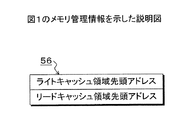
図2は図1の揮発メモリ32に展開されているメモリ管理情報56を示した説明図である。図2において、メモリ管理情報56にはライトキャッシュ領域先頭アドレスとリードキャッシュ領域先頭アドレスが格納されている。
FIG. 2 is an explanatory diagram showing the
このようにライトキャッシュ領域58とリードキャッシュ領域60の先頭アドレスが決まると、ホスト11からのライトコマンドまたはリードコマンドに伴うライトデータ及びリードデータの記憶の際には、予め定めた例えば16セクタのページと呼ばれるキャッシュデータ格納領域を確保しながら、ページ区分内にライトデータ又はリードデータをキャッシュデータとして格納する。
When the start addresses of the
図1のMPU28に設けたメモリ配置変更部54は、不揮発メモリ42に配置しているライトキャッシュ領域58のライトキャッシュデータを全て磁気ディスク側に書き込んで空にするタイミング毎に、フラッシュメモリを用いた不揮発メモリ42のセクタ単位より小さい所定のアドレスサイズ単位、具体的には本実施形態にあっては磁気ディスクの1セクタサイズ単位または磁気ディスクの1ワード単位(1ワードは例えば8バイト)ずつライトキャッシュ領域58を巡回させるようにメモリ管理情報56を変更する。即ちメモリ管理情報に登録している図2に示すライトキャッシュ領域先頭アドレスを変更する。
The memory arrangement changing unit 54 provided in the
メモリ配置管理部52の処理はリードキャッシュ領域60についても基本的に同様であり、不揮発メモリ42に配置したリードキャッシュ領域60のリードキャッシュデータを全て無効化して空にするタイミング毎に、フラッシュメモリを用いた不揮発メモリ42の消去単位より小さい所定のアドレスサイズ単位、例えば1セクタサイズ単位または1ワード単位ずつリードキャッシュ領域60を巡回させるようにメモリ管理情報56を変更する。即ち、メモリ管理情報に登録している図2に示すリードキャッシュ領域先頭アドレスを変更する。
The processing of the memory
ここでMPU28に設けたメモリ配置変更部54において、ライトキャッシュ領域58を巡回させるようにメモリ管理情報を変更するタイミングは、ライトキャッシュ領域58のライトキャッシュデータを全て磁気ディスク側に書き込んだタイミングとなるが、このタイミングとしては次のものがある。
(1)ホスト11からフラッシュキャッシュコマンドを受信してライトキャッシュ領域58のライトキャッシュデータを磁気ディスクに書き込んだタイミング。
(2)ライトキャッシュ領域58が一杯となって全てのライトキャッシュデータを磁気ディスク側に書き込んだタイミング。
(3)予め定めた一定時間経過時に前記(1)あるいは(2)によりライトキャッシュ領域58を一度も空にすることがなかった時に、強制的にライトキャッシュ領域の全てのライトキャッシュデータを磁気ディスク側に書き込んで空とするタイミング。
(4)所定のライトコマンド発行回数に達しても一度もライトキャッシュ領域58を空にすることがなかった時に、強制的にライトキャッシュ領域58の全てのライトキャッシュデータを磁気ディスク側に書き込んで空としたタイミング。
Here, in the memory arrangement changing unit 54 provided in the
(1) Timing at which the flash cache command is received from the
(2) Timing when the
(3) When the
(4) If the
このような(1)〜(4)に示すタイミングが発生する毎に、メモリ配置変更部54はライトキャッシュ領域58のメモリ管理情報56に登録している領域先頭アドレスを1セクタサイズ単位または1ワード単位にずらすことによって、ライトキャッシュ領域58を巡回させるように変更して再配置する処理を繰り返す。
Each time the timings shown in (1) to (4) occur, the memory arrangement changing unit 54 sets the area start address registered in the
メモリ配置変更部54によるリードキャッシュ領域60を巡回させるようにメモリ管理情報56を変更するタイミングは、本実施形態にあっては、ホスト11からリードキャッシュ入れ替えコマンドを受けたタイミングとする。
In this embodiment, the timing at which the
しかし、リードキャッシュ入れ替えコマンドを受けたタイミングで、リードキャッシュ領域60の場合には、リードキャッシュ領域60を空にするためにリードキャッシュ領域60に格納しているリードデータを磁気ディスク側に書き込む必要ななく、リードキャッシュ領域60に格納している全リードデータを無効化するだけでよい。リードデータの無効化は図示しないキャッシュ管理情報における有効データを示す有効フラグをリセットして無効化すればよい。 However, in the case of the read cache area 60 at the timing of receiving the read cache replacement command, it is necessary to write the read data stored in the read cache area 60 to the magnetic disk side in order to make the read cache area 60 empty. Instead, all the read data stored in the read cache area 60 need only be invalidated. The invalidation of the read data may be invalidated by resetting a valid flag indicating valid data in cache management information (not shown).
図3は本実施形態におけるライトキャッシュ領域のページ区分と不揮発メモリ消去単位のウエアレベリングを示した説明図である。 FIG. 3 is an explanatory diagram showing the page classification of the write cache area and the wear leveling of the nonvolatile memory erasing unit in the present embodiment.
図3(A)においてライトキャッシュ領域58はページP1〜Pnという区分に分割されており、ページP1〜Pnのページサイズ66は例えば磁気ディスクの16セクタサイズである。ここで磁気ディスクの1セクタを1024バイトとすると、ページサイズ66の16セクタは16KBに相当する。
In FIG. 3A, the
一方、ライトキャッシュ領域58が配置された本実施形態で不揮発メモリ42として使用するフラッシュメモリは、例えばページサイズ66に一致した16KBを消去単位として動作する。即ちライトキャッシュ領域58はページP1〜Pn単位に書き換えることができる。
On the other hand, the flash memory used as the
このようなフラッシュメモリの消去単位に一致するページサイズ66を持つライトキャッシュ領域58の構成について、従来は消去単位に一致するページサイズ66単位にライトキャッシュデータを巡回させるようにずらすウエアレベリングを行っている。
With respect to the configuration of the
図3(B)は図3(A)のライトキャッシュ領域58につきキャッシュデータを消去単位である1ページサイズだけずらした状態の説明図である。図3(B)において、ずらす前の図3(A)のページP1のライトキャッシュデータが次のページP2に移動し、以下残りのページP3〜Pnについてもひとつ後ろのページそのままライトキャッシュデータが移動している。
FIG. 3B is an explanatory diagram of a state in which the cache data is shifted by one page size which is an erasing unit for the
このためページP1〜Pnの区分内をみると、各ページの先頭側のセクタについてキャッシュデータが書き込まれ、ページ区分の後半の空き領域はウエアレベリングを行ってもそのまま空き領域となっている。その結果、ページ区分内において書き込み回数の多い部分と書き込み回数の少ない部分がそのまま残存し、ページ区分内で書き込み回数が均一化するためのウエアレベリングの処理効果はほとんど期待できない。 For this reason, in the section of pages P1 to Pn, cache data is written in the sector on the head side of each page, and the free area in the second half of the page section remains as it is even if wear leveling is performed. As a result, a portion with a large number of writes and a portion with a small number of writes remain as they are in the page section, and a wear leveling processing effect for making the number of writes uniform in the page section is hardly expected.
このような問題に対し本実施形態にあっては、図4に示すような不揮発メモリの消去単位より小さい単位ずつライトキャッシュ領域を巡回させることで、ページ区分内における書き込み回数の多い部分と少ない部分を均一化する効率的なウエアレベリングを実現することができる。 In this embodiment, for such a problem, the write cache area is cycled in units smaller than the erase unit of the nonvolatile memory as shown in FIG. It is possible to realize efficient wear leveling that equalizes.
図4(A)はウエアレベリング前のライトキャッシュ領域58である。これは図3(A)と同じである。ページP1〜Pnのサイズは不揮発メモリ42で使用するフラッシュメモリの消去単位と同じ16KBとなっている。
FIG. 4A shows the
ここで、例えば図4(A)のライトキャッシュ領域58におけるメモリ管理情報56に登録されているライトキャッシュ領域先頭アドレスがページP1の先頭を示す領域先頭アドレス72−1であったとする。
Here, for example, it is assumed that the write cache area start address registered in the
この状態で本実施形態の磁気ディスクの1セクタサイズ単位だけ領域先頭アドレス72−1を後方にずらすメモリ管理情報56の変更を行うと、変更後のメモリ管理情報56に基づき、図4(B)のように、最後のページPnの後ろ側に領域先頭アドレス72−2が設定され、領域先頭アドレス72−2を起点に図4(A)と同じライトデータがもし格納されたとすると、図示のように1セクタサイズ単位ずつずれてページ区分内に格納する。
In this state, when the
更に図4(C)のように1セクタサイズずれて領域先頭アドレス72−3となると各ページ内で更に1セクタサイズ分ライトキャッシュデータが後方側にずれることになる。 Further, as shown in FIG. 4C, when the sector start address 72-3 is shifted by one sector size, the write cache data is further shifted backward by one sector size within each page.
このようなページ区分に分割されたライトキャッシュ領域58につき、図3(B)に示したようなフラッシュメモリのページサイズに位置する消去単位でずらす場合に比べ、消去単位より小さなセクタサイズ単位もしくは更に小さな1ワード単位ずつキャッシュ領域先頭アドレスを巡回するようにずらすことで、ページ内をライトキャッシュデータが1セクタサイズ単位ずつまたは1ワード単位ずつ移動しながら巡回的に格納されることになり、ページ区分内における書き込み回数の多い部分と書き込み回数の少ない部分は効率的に均一化され、ウエアレベリングによる十分な効果が得られ、その結果、ライトキャッシュ領域58を配置している不揮発メモリ42の書替え処理を大幅にのばすことができる。
Compared with the case where the
このような図4に示す1セクタサイズ単位もしくは1ワード単位に巡回的に領域先頭アドレスをずらすようにメモリ管理情報を変更する処理は、図1のリードキャッシュ領域60についても同様である。 The process for changing the memory management information so as to shift the area head address cyclically in units of one sector size or in units of words shown in FIG. 4 is the same for the read cache area 60 of FIG.
図5は本実施形態の不揮発メモリ42における消去単位のデータの書き込み処理を示して説明図である。
FIG. 5 is an explanatory diagram showing a process of writing data in erase units in the
図5(A)において、不揮発メモリ42は消去単位となる領域70−1〜70−nに分割されている。消去単位となる70−1〜70−nは、図3に示したようにページサイズ66と同じ16KBである。
In FIG. 5A, the
ここで領域70−2に含まれるデータを書き変える場合には、領域70−2をバッファメモリ40に読み出して領域70−21として配置する。この状態で領域70−21の中に例えばライトコマンドに基づいて受信したライトデータ74を書き込む。
Here, when the data included in the area 70-2 is rewritten, the area 70-2 is read into the buffer memory 40 and arranged as the area 70-21. In this state, the
バッファメモリ40におけるライトデータ74の書込みが済むと、書き込みの済んだ領域70−21のデータを不揮発メモリ42の領域70−2に書き込み、これによってライトデータ74がライトデータ74−1として不揮発メモリ42に書き込まれることになる。
When the
図6は本実施形態によるライトキャッシュ領域に対するウエアレベリング処理の手順を詳細に示した説明図である。図6(A)は図3または図4に示したライトキャッシュ領域58を直線的に並べたひとつの領域として示しており、上側に示す数値0〜n−1がページ番号である。
FIG. 6 is an explanatory diagram showing in detail the procedure of the wear leveling process for the write cache area according to the present embodiment. FIG. 6A shows the
このライトキャッシュ領域58−1にはライトキャッシュデータ62−1〜62−4が格納されており、白地の部分が空き領域64−1〜64−3となっている。 Write cache data 62-1 to 62-4 is stored in the write cache area 58-1, and white areas are empty areas 64-1 to 64-3.
この状態でメモリ管理情報56−1の同期内容はライトキャッシュ領域58−1の先頭位置を示す領域先頭アドレス66−1となっている。 In this state, the synchronization content of the memory management information 56-1 is an area head address 66-1 indicating the head position of the write cache area 58-1.
図6(A)のようなライトキャッシュデータのライトキャッシュ領域58−1に対する格納領域で、全てのキャッシュデータ62−1〜62−4は例えばホストからのフラッシュコマンドを受領した際に、全て磁気ディスク22に書き込まれ、図6(B)のライトキャッシュ領域58−2に示すように空になる。 In the storage area for the write cache area 58-1 of the write cache data as shown in FIG. 6A, all the cache data 62-1 to 62-4 are all magnetic disks when a flush command is received from the host, for example. 22 and is emptied as shown in the write cache area 58-2 in FIG.
このようにライトキャッシュ領域58−2が空となったタイミングで、図1のMPU28に設けたメモリ配置変更部54がメモリ管理情報56−1の領域先頭アドレス66−1を例えば1セクタサイズ単位だけ後方にずらす管理情報更新処理62を実行する。
As described above, at the timing when the write cache area 58-2 becomes empty, the memory arrangement changing unit 54 provided in the
メモリ管理情報56−1の更新が行われたならば、この情報はメモリ構成を示す重要な情報であるため、磁気ディスク22にメモリ管理情報56−02として書き込みを行い、磁気ディスク22に対する書込みが成功した後に、図6(C)に示すように不揮発メモリに展開しているメモリ管理情報56−1を管理情報更新処理64によって変更した新たなメモリ管理情報56−2に書き換える。
If the memory management information 56-1 is updated, this information is important information indicating the memory configuration. Therefore, the memory management information 56-02 is written to the
このメモリ管理情報56−2への書替により、図6(C)のライトキャッシュ領域58−3に示すように、それまで0ページの先頭にセットされていた領域先頭アドレス62−1が、ライトキャッシュ領域58−4に示すように、1セクタサイズ単位だけ後方にずれた領域先頭アドレス62−2となり、ここを起点にページ番号0〜n−1で示すページ区分が行われる。
By rewriting to this memory management information 56-2, as shown in the write cache area 58-3 in FIG. 6C, the area head address 62-1 that has been set at the head of
即ち、ライトキャッシュ領域58−3の状態からライトキャッシュデータはライトキャッシュ領域58−4に示すように1セクタサイズ単位後方にずれた配置となる。 That is, the write cache data is shifted from the state of the write cache area 58-3 by one sector size unit as shown in the write cache area 58-4.
続いて図6(D)に示すように、変更後のメモリ管理情報56−2に基づくライトキャッシュ領域58−5に配置について、図6(A)に示すと同じライトキャッシュデータ62−1〜62−4の格納が仮に行われたとすると、図6(A)の先頭ページとなる0ページ側のライトキャッシュデータ62−1は、図6(D)の変更後にあっては、後方側のライトキャッシュデータ62−31と前方側のライトキャッシュデータ62−32に分かれ、またその間のライトキャッシュデータについては後方に1セクタサイズ単位ずれた位置にライトキャッシュデータ62−1〜62−4として格納されている。 Subsequently, as shown in FIG. 6D, the same write cache data 62-1 to 62-62 as shown in FIG. 6A is arranged in the write cache area 58-5 based on the memory management information 56-2 after the change. -4 is temporarily stored, the write cache data 62-1 on the 0 page side, which is the first page in FIG. 6A, is stored in the write cache on the rear side after the change in FIG. 6D. It is divided into data 62-31 and write cache data 62-32 on the front side, and the write cache data between them is stored as write cache data 62-1 to 62-4 at positions shifted backward by one sector size unit. .
このようにして本発明はライトキャッシュ領域のライトキャッシュデータが全て磁気ディスク装置に格納されて空となるタイミング毎に、例えば1セクタサイズ後方に領域先頭アドレスを巡回的にずらすメモリ管理情報の変更が行われ、ライトキャッシュ領域に格納されているライトキャッシュデータはもしライトキャッシュデータに変更がなければ、順次キャッシュ領域をセクタサイズずつずれながら巡回することになり、領域内にランダムに空き領域を生じていても1セクタサイズ単位の巡回を繰り返すことで、書き込み回数の多い部分と少ない部分が均一化され、不揮発メモリ42として使用しているフラッシュメモリの寿命を延ばすことができる。
Thus, according to the present invention, at every timing when all the write cache data in the write cache area is stored in the magnetic disk device and becomes empty, for example, the memory management information is changed by cyclically shifting the area start address backward by one sector size. If the write cache data stored in the write cache area is not changed, if the write cache data is not changed, the cache area is sequentially cycled while shifting by the sector size, and a free area is randomly generated in the area. However, by repeating the cycle in units of one sector size, a portion with a large number of writes and a portion with a small number of writes are made uniform, and the life of the flash memory used as the
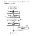
図7及び図8はウエアレベリングを含む本実施形態のハードウェア型磁気装置の制御処理を示したフローチャートである。図7において、ホスト11の起動に伴って磁気ディスク装置10に電源が投入されるとステップS1で初期化起動処理が行われる。
7 and 8 are flowcharts showing control processing of the hardware type magnetic apparatus of this embodiment including wear leveling. In FIG. 7, when the power is turned on to the magnetic disk device 10 as the
初期化自動処理は不揮発メモリ34のフラッシュROMなどに格納されているブートプログラムの実行によりOSとして機能するファームウエアを例えば磁気ディスク22−1、22−2側の記録面のシステム領域から揮発メモリ32に読出し配置し、MPU28により実行する。
In the initialization automatic processing, firmware that functions as an OS by executing a boot program stored in a flash ROM or the like of the
続いてステップS2で磁気ディスクの例えばシステム領域に格納しているメモリ管理情報を読出し、揮発メモリ32に図1に示すようにメモリ管理情報56として配置する。
Subsequently, in step S2, the memory management information stored in, for example, the system area of the magnetic disk is read and arranged in the
続いてステップS3でホスト11からのコマンド受信を判別すると、ステップS4でライトコマンドか否か判別する。ライトコマンドであった場合にはホスト11側から転送されたライトデータはホストインタフェース制御部38、バッファ制御部44を介して、一端バッファメモリ40に保持する。
Subsequently, when it is determined in step S3 that a command is received from the
この状態でキャッシュ制御部50は不揮発メモリ42のライトキャッシュ領域58に該当するデータが存在するか否かのライトキャッシュヒットの有無をチェックする。ライトキャッシュヒットとなった場合には、ステップS6でライトキャッシュ領域58のデータを更新し、磁気ディスク側にライトキャッシュデータを書き込むことなくホスト11に対しライトコマンドの正常終了を応答する。
In this state, the cache control unit 50 checks whether or not there is a write cache hit as to whether or not the corresponding data exists in the
ステップS5でライトキャッシュがミスヒットとなった場合には、ステップS7でライトキャッシュ領域に新たにページを確保し、このページ内にライトデータを格納し、この場合にも磁気ディスク側にライトデータを書き込むことなくホスト11に対しライトコマンドの正常終了を応答する。
If the write cache becomes a miss hit in step S5, a new page is secured in the write cache area in step S7, write data is stored in this page, and in this case also write data is stored on the magnetic disk side. A normal end of write command is returned to the
一方、ステップS8でリードコマンドであることが判別されると、ステップS9で不揮発メモリ42のリードキャッシュ領域60を調べ、該当するリードデータが存在するか否かのリードキャッシュヒットの有無を判別する。
On the other hand, if it is determined in step S8 that the command is a read command, the read cache area 60 of the
リードキャッシュヒットとなった場合にはステップS10でリードキャッシュ領域60から該当するデータをバッファメモリ40に読出した後にホスト11にリードデータを転送する。
If a read cache hit occurs, the corresponding data is read from the read cache area 60 to the buffer memory 40 in step S10, and then the read data is transferred to the
ステップS9でリードキャッシュがミスヒットとなった場合には、ステップS11で磁気ディスク側からヘッドIC26、リードチャネル48、フォーマット制御部46を介してデータを読出し、バッファ制御部44でバッファメモリ40に格納した後、ホストインタフェース制御部38を介してリードデータをホスト11に転送する。続いてステップS12でバッファメモリ40に格納しているリードデータをリードキャッシュ領域60に格納する。
If the read cache results in a miss hit in step S9, data is read from the magnetic disk side via the
次に図8のステップS13でホスト11からのフラッシュキャッシュコマンドの受信の有無をチェックしており、フラッシュキャッシュコマンドを判別するとステップS14に進み、不揮発メモリ42上のライトキャッシュ領域58の全てのキャッシュデータを磁気ディスク側に書き込んで空にする。
Next, in step S13 of FIG. 8, it is checked whether or not a flash cache command is received from the
続いてステップS15でホスト11からのリードキャッシュ入れ替えコマンドの受信の有無をチェックしており、リードキャッシュ入れ替えコマンドの受信を判別するとステップS16に進み、不揮発メモリ42上のリードキャッシュ領域60の全てのリードキャッシュデータを無効化して空にする。
In step S15, it is checked whether or not a read cache replacement command is received from the
次にステップS17に進み、ライトキャッシュ領域58が空か否か判別し、空であった場合にはステップS18に進み、ライトキャッシュのウエアレベリングを実行する。
In step S17, it is determined whether or not the
続いてステップS19でリードキャッシュ領域60が空であることが判別されるとステップS20に進み、リードキャッシュ領域60のウエアレベリングを実行する。 Subsequently, when it is determined in step S19 that the read cache area 60 is empty, the process proceeds to step S20, and wear leveling of the read cache area 60 is executed.
続いてステップS21で停止指示の有無をチェックしており、停止指示があるまでステップS13からの指示を繰り返し、停止指示を判別するとステップS22で揮発メモリ32上のメモリ管理情報56を磁気ディスク側に格納した後に処理を終了する。
Subsequently, in step S21, the presence or absence of a stop instruction is checked. The instruction from step S13 is repeated until the stop instruction is issued. When the stop instruction is determined, the
一方、図7のステップS3でホスト11からのコマンド受信のないアイドル状態にあってはステップS23においてアイドルでのウエアレベリングを実行する。
On the other hand, in the idle state in which no command is received from the
図9は図8のステップS18に示したライトキャッシュウエアレベリングの詳細を示したフローチャートである。図9において、ライトキャッシュウエアレベリングは、ステップS1で揮発メモリ32上のメモリ管理情報56における図2に示したライトキャッシュ先頭アドレスを例えば磁気ディスクの1セクタサイズ分だけ減少させることにより、磁気ディスク装置上におけるライトキャッシュ領域を1セクタサイズだけずらした新配置に更新する。
FIG. 9 is a flowchart showing details of the write cache wear leveling shown in step S18 of FIG. In FIG. 9, write cache wear leveling is performed by reducing the write cache head address shown in FIG. 2 in the
続いてステップS2で更新済みメモリ管理情報56を磁気ディスク装置側のシステム領域に書き込む。即ちメモリ管理情報は不揮発メモリ42におけるメモリ構成を示す重要な情報であるため、揮発メモリ32上で更新したメモリ管理情報56を一端磁気ディスク側に書き込んで保存し、障害などによる磁気ディスク装置の電源遮断などにより揮発メモリ32上の更新済みのメモリ管理情報56が失われないようにしている。
In step S2, the updated
続いてステップS3で更新済みメモリ管理情報の磁気ディスク側の書き込みの成功を判別するとステップS4に進み、新配置となる更新済みメモリ管理情報を有効化し、更新済みメモリ管理情報を使用して現在空となっているライトキャッシュ領域58に対するライトコマンドに伴うライトデータの書き込みを開始することになる。
Subsequently, when it is determined in step S3 that writing of the updated memory management information on the magnetic disk side is successful, the process proceeds to step S4, where the updated memory management information to be newly arranged is validated, and the current memory is empty using the updated memory management information. Writing of the write data accompanying the write command to the
一方、ステップS3で磁気ディスク側の書込みが不成功であった場合には、ステップS5でメモリ管理情報の更新を無効化し、更新前メモリ管理情報によるライトキャッシュ領域58の配置を維持する。
On the other hand, if the writing on the magnetic disk side is unsuccessful in step S3, the update of the memory management information is invalidated in step S5, and the arrangement of the
図10は図8のステップS20に示したリードキャッシュウエアレベリングの詳細を示したフローチャートである。図10において、リードキャッシュウエアレベリングはステップS1でリードキャッシュ領域60が空となっていることが条件に揮発メモリ32上のメモリ管理情報56における図2に示したリードキャッシュ先頭アドレスを例えば磁気ディスクの1セクタサイズだけ減少させることによりずらし、これにより不揮発メモリ42上のリードキャッシュ領域60を新配置に更新する。
FIG. 10 is a flowchart showing details of the read cache wear leveling shown in step S20 of FIG. In FIG. 10, the read cache wear leveling uses the read cache head address shown in FIG. 2 in the
続いてステップS2で更新済みメモリ管理情報56を揮発メモリ32から磁気ディスクのシステム領域に書き込んで保存し、ステップS3で磁気ディスク側の書き込み成功が判別されるとステップS4で新配置となった更新済みメモリ管理情報を有効化する。
Subsequently, in step S2, the updated
これにより不揮発メモリ42上のリードキャッシュ領域60はウエアレベリング前に対し1セクタサイズだけアドレスを減少する方向にずれた位置を領域先頭位置として配置されてホストからのリードコマンドに伴うリードデータを格納する。
As a result, the read cache area 60 on the
またステップS3で磁気ディスクに対する書込みが不成功であった場合にはステップS5でメモリ管理情報の更新を無効化し、ウエアレベリング前のメモリ管理情報を維持する。 If writing to the magnetic disk is unsuccessful in step S3, the update of the memory management information is invalidated in step S5, and the memory management information before wear leveling is maintained.
図11は図7のステップS23に示したアイドルウエアレベリング処理の詳細を示したフローチャートである。図11において、アイドルウエアレベリング処理は、ステップS1で不揮発メモリ42上のライトキャッシュ領域56が一杯か否か判別し、一杯であればステップS4に進み、全ライトキャッシュデータを磁気ディスク側に書き込んでライトキャッシュ領域58をウエアレベリングのために空にする。
FIG. 11 is a flowchart showing details of the idle wear leveling process shown in step S23 of FIG. In FIG. 11, in the idle wear leveling process, it is determined in step S1 whether or not the
ステップS1でライトキャッシュが一杯でなかった場合にはステップS2に進み、前回のライトキャッシュデータが空となってウエアレベリングした時から一定時間経過したか否かチェックする。一定時間を経過した場合にはステップS3に進み、ライトキャッシュ領域が一回でも空になったことがあるか否かチェックし、空になったことがなければステップS5でライトキャッシュ領域58の全ライトキャッシュデータを磁気ディスク装置に強制的に書き込んで空にする。 If the write cache is not full in step S1, the process proceeds to step S2, and it is checked whether or not a predetermined time has elapsed since the previous write cache data became empty and wear leveling was performed. If the fixed time has elapsed, the process proceeds to step S3, where it is checked whether the write cache area has been emptied at least once. Write cache data is forcibly written to the magnetic disk device to be emptied.
ステップS1で一定時間を経過していない場合にはステップS4に進み、前回のライトキャッシュ領域を空にしてウエアレベリングした時から現在までのライトコマンド発行数を取得し、ライトコマンド発行数が閾値に達成したか否か判別する。 If the predetermined time has not elapsed in step S1, the process proceeds to step S4, where the previous write cache area is emptied and wear leveling is performed until the current write command issuance number is acquired. Determine whether it has been achieved.
ライトコマンド発行数が閾値に達成していた場合にはステップS3に進み、ライトキャッシュ領域が一回でも空になったことがあるか否か判別し、空になったことがなければステップS5でライトキャッシュ領域58の全ライトキャッシュデータを磁気ディスク側に強制的に書き込んで空にする。
If the write command issuance number has reached the threshold value, the process proceeds to step S3 to determine whether or not the write cache area has been emptied even once. All write cache data in the
続いてステップS6でライトキャッシュ領域58が空であるか否かチェックし、空であった場合にはステップS7でライトキャッシュのウエアレベリングを実行する。このステップS7のライトキャッシュのウエアレベリングは図9のフローチャートに示した内容と同じになる。
In step S6, it is checked whether the
またステップS8でリードキャッシュ領域60が空であることが判別されると図9に進み、図10に示したと同じリードキャッシュ領域のウエアレベリングを実行する。 If it is determined in step S8 that the read cache area 60 is empty, the process proceeds to FIG. 9, and the same wear leveling of the read cache area as shown in FIG. 10 is executed.
このように本実施形態の磁気ディスクにおける不揮発メモリ42上に配置したライトキャッシュ領域58とリードキャッシュ領域60の場所による書き込み回数を平均化するウエアレベリングは、図7のステップS13、S15に示したホスト11からのフラッシュキャッシュコマンドやリードキャッシュ入れ替えコマンドに基づくライトキャッシュ領域58を空としたタイミングで行う以外に、図11のアイドルウエアレベリングに示したように、ホスト11からのコマンドに依存せず、磁気ディスク装置10側における装置自身の処理として例えばライトキャッシュについてはライトキャッシュ領域58が一杯になったとき、前回のウエアレベリングから一定時間を経過した後に一回もライトキャッシュが空にならなかったとき、あるいはライトコマンド発行数が閾値に達した時に同じくライトキャッシュが一回も空にならなかったとき、強制的にライトキャッシュ領域58の全ライトキャッシュデータを磁気ディスク側に書きこんで空として、このタイミングでライトキャッシュ領域のウエアレベリングを行えるようにしている。
As described above, the wear leveling that averages the number of times of writing depending on the locations of the
また本発明は図1の磁気ディスク10に設けたMPU28により実行するプログラムを提供するものであり、このプログラムは図7〜図11のフローチャートに示した内容を持つ。
Further, the present invention provides a program executed by the
尚、上記の実施形態にあってはホストからフラッシュキャッシュコマンドを受けた際に、ライトキャッシュ領域58の全てのライトキャッシュデータを磁気ディスク側に書き込んで空にするようにしているが、ライトキャッシュ領域58を複数領域に分割し、フラッシュキャッシュコマンドを受ける事に順次分割したライトキャッシュ領域のライトキャッシュデータを磁気ディスク装置に書き込んで空とし、分割したライトキャッシュ領域ごとにウエアレベリングを実行するようにしてもよい。
In the above embodiment, when the flash cache command is received from the host, all the write cache data in the
この点はリードキャッシュ領域60についても同様であり、リードキャッシュ領域60を複数領域に分割してホストからのリードキャッシュ入れ替えコマンドを受けた際に順次分割したリードキャッシュ領域を無効化して空にすることで、リードキャッシュのウエアレベリングを実行するようにしてもよい。 This also applies to the read cache area 60. When the read cache area 60 is divided into a plurality of areas and the read cache replacement command is received from the host, the sequentially divided read cache areas are invalidated and made empty. Thus, wear leveling of the read cache may be executed.
このようにライトキャッシュ領域58及びリードキャッシュ領域60を複数領域に分割してキャッシュ領域を空にした状態でウエアレベリングを行うことで、ウエアレベリングの際にも対象外となる領域のキャッシュデータを残すことができ、全てのキャッシュデータを除いて空にした場合と比べ、キャッシュデータが一部残ることでホスト11に対するキャッシュ利用による入出力性能の低下を最小限に抑えることができる。
In this way, by performing the wear leveling in a state where the
また上記の実施形態にあっては図3(A)のように、ページサイズ66とフラッシュメモリの消去単位を同じとした場合を例にとっているが、フラッシュメモリの消去単位としてはそれ以外にページサイズの整数倍となる32KB、64KBなど適宜の消去単位をもつフラッシュメモリが使用できる。
In the above embodiment, as shown in FIG. 3A, the case where the
また、不揮発メモリの書き換えにおいて、消去処理が不要となった場合であっても、書き換え回数に制限がある限り,本方式は有効である。なぜなら、キャッシュの管理をページ単位でおこなうことによる使用頻度の偏りを解消する必要があるからである。 In addition, even when the erasing process is not necessary in the rewriting of the nonvolatile memory, this method is effective as long as the number of rewritings is limited. This is because it is necessary to eliminate the uneven usage frequency caused by managing the cache in units of pages.
また本発明はその目的と利点を損なうことのない適宜の変形を含み、また上記の実施形態に示した数値による限定は受けない。 The present invention includes appropriate modifications that do not impair the object and advantages thereof, and is not limited by the numerical values shown in the above embodiments.
ここで本発明の特徴をまとめて列挙すると次の付記のようになる。
(付記)
(付記1)(装置:ライトキャッシュ)
ヘッドによりデータを記録して再生するディスク媒体と、
ライトキャッシュ領域が配置される不揮発メモリと、
上位装置のライト要求により前記ディスク媒体に記録するライトデータを前記ライトキャッシュ領域に一時的に格納するキャッシュ制御部と、
前記不揮発メモリにおける前記ライトキャッシュ領域の配置位置を示すメモリ管理情報を前記ディスク媒体に格納して管理するメモリ配置管理部と、
前記不揮発メモリに配置したライトキャッシュ領域のライトキャッシュデータを全て前記ディスク媒体に書き込んで空にする毎に、前記不揮発メモリの消去単位より小さい所定のアドレスサイズ単位ずつ前記ライトキャッシュ領域を巡回させるように前記メモリ管理情報を変更するメモリ配置変更部と、
を備えたことを特徴とする記憶装置。(1)
(付記2)(追加:先頭アドレス)
付記1記載の記憶装置に於いて、
前記メモリ配置管理部は前記メモリ管理情報に前記ライトキャッシュ領域の領域先頭アドレスを登録して管理し、
前記メモリ配置変更部は、前記メモリ管理情報に登録している前記領域先頭アドレスを前記所定のアドレス単位だけずらすことを特徴とする記憶装置。(2)
(付記3)(オリジナル2:電源投入時の読出配置)
付記1記載の記憶装置に於いて、前記メモリ配置管理部は、電源投入時に前記メモリ管理情報を前記ディスク媒体上から読み出して揮発メモリに配置することを特徴とする記憶装置。
Here, the features of the present invention are enumerated as follows.
(Appendix)
(Appendix 1) (Device: Write cache)
A disk medium for recording and reproducing data by a head;
A non-volatile memory in which the write cache area is arranged;
A cache control unit for temporarily storing write data to be recorded on the disk medium in response to a write request from a host device in the write cache area;
A memory arrangement management unit that stores and manages memory management information indicating an arrangement position of the write cache area in the nonvolatile memory in the disk medium;
Each time the write cache data in the write cache area arranged in the non-volatile memory is all written to the disk medium and emptied, the write cache area is circulated by a predetermined address size unit smaller than the erase unit of the non-volatile memory. A memory arrangement changing unit for changing the memory management information;
A storage device comprising: (1)
(Appendix 2) (Addition: Start address)
In the storage device according to
The memory arrangement management unit registers and manages the area start address of the write cache area in the memory management information,
The memory arrangement changing unit shifts the area start address registered in the memory management information by the predetermined address unit. (2)
(Supplementary note 3) (Original 2: Reading arrangement at power-on)
The storage device according to
(付記4)(追加:メモリ管理情報の媒体書込)
付記3記載の記憶装置に於いて、前記メモリ配置管理部は、前記揮発メモリ上で前記メモリ管理情報を変更した時、変更したメモリ管理情報を前記ディスク媒体に書込み、前記ディスク媒体への書込み成功を条件に、変更後のメモリ管理情報を使用して管理することを特徴とする記憶装置。
(Appendix 4) (Addition: Memory management information writing to medium)
The storage device according to
(付記5)(オリジナル3:1セクタ巡回)
付記1記載の記憶装置に於いて、前記メモリ配置変更部は、前記メモリ管理情報を前記ディスク媒体の1セクタサイズ単位ずつ巡回させるように変更することを特徴とする記憶装置。
(Appendix 5) (Original 3: 1 sector patrol)
The storage device according to
(付記6)(オリジナル4:1ワード巡回)
付記1記載の記憶装置に於いて、前記メモリ配置変更部は、前記メモリ管理情報を前記ディスク媒体の1ワード単位ずつ巡回させるように変更することを特徴とする記憶装置。
(Appendix 6) (Original 4: 1 word patrol)
The storage device according to
(付記7)(追加:コマンド等による書込み)
付記1記載の記憶装置に於いて、前記キャッシュ制御部は、前記上位装置から所定のコマンドを受信した時、及び、前記ライトキャッシュ領域がライトキャッシュデータで一杯となった時または空き容量が所定値以下となった時に、前記ライトキャッシュ領域の全てのライトキャッシュデータを前記ディスク媒体に書き込んで空とすることを特徴とする記憶装置。
(Appendix 7) (Add: Write by command etc.)
The storage device according to
(付記8)(オリジナル5、6:強制書込み)
付記1記載の記憶装置に於いて、前記メモリ配置変更部は、前記不揮発メモリに配置したライトキャッシュ領域のライトキャッシュデータが所定時間を経過しても空にならない時、及び所定のライト要求発行回数に達しても空にならない時、強制的に、前記ライトキャッシュ領域の全てのライトキャッシュデータを前記ディスク媒体に書き込んで空にすることを特徴とする記憶装置。
(Appendix 8) (
In the storage device according to
(付記9)(装置:リードキャッシュ)
ヘッドによりデータを記録して再生するディスク媒体と、
リードキャッシュ領域が配置される不揮発メモリと、
上位装置のリード要求により前記ディスク媒体から再生したリードデータを前記リードキャッシュ領域に一時的に格納するキャッシュ制御部と、
前記不揮発メモリにおける前記リードキャッシュ領域の配置位置を示すメモリ管理情報を前記ディスク媒体に格納して管理するメモリ配置管理部と、
前記不揮発メモリに配置したリードキャッシュ領域のリードキャッシュデータの一部または全て無効化して空にする毎に、前記不揮発メモリの消去単位より小さい所定のアドレスサイズ単位だけ前記リードキャッシュ領域を巡回させるように前記メモリ管理情報を変更するメモリ配置変更部と、
を備えたことを特徴とする記憶装置。(3)
(付記10)(追加:先頭アドレス)
付記9記載の記憶装置に於いて、
前記メモリ配置管理部は前記メモリ管理情報に前記リードキャッシュ領域の領域先頭アドレスを登録して管理し、
前記メモリ配置変更部は、前記メモリ管理情報に登録している前記領域先頭アドレスを前記所定のアドレス単位だけずらすことを特徴とするディスク装置。(4)
(付記11)(オリジナル2:電源投入時の読出配置)
付記9記載の記憶装置に於いて、前記メモリ配置管理部は、電源投入時に前記メモリ管理情報を前記ディスク媒体上から読み出して揮発メモリに配置することを特徴とするディスク装置。
(Appendix 9) (Device: Read Cash)
A disk medium for recording and reproducing data by a head;
A nonvolatile memory in which a read cache area is arranged;
A cache controller that temporarily stores read data reproduced from the disk medium in response to a read request from a host device in the read cache area;
A memory arrangement management unit that stores and manages memory management information indicating an arrangement position of the read cache area in the nonvolatile memory in the disk medium;
Each time the read cache data in the read cache area arranged in the nonvolatile memory is partially or completely invalidated and emptied, the read cache area is circulated by a predetermined address size unit smaller than the erase unit of the nonvolatile memory. A memory arrangement changing unit for changing the memory management information;
A storage device comprising: (3)
(Appendix 10) (Addition: Start address)
In the storage device according to appendix 9,
The memory arrangement management unit registers and manages the area start address of the read cache area in the memory management information,
The disk device, wherein the memory arrangement changing unit shifts the area head address registered in the memory management information by the predetermined address unit. (4)
(Appendix 11) (Original 2: Readout layout at power-on)
The storage device according to appendix 9, wherein the memory placement management unit reads the memory management information from the disk medium and places it in a volatile memory when power is turned on.
(付記12)(追加:メモリ管理情報の媒体書込)
付記11記載の記憶装置に於いて、前記メモリ配置管理部は、前記揮発メモリ上で前記メモリ管理情報を変更した時、変更したメモリ管理情報を前記ディスク媒体に書込み、前記ディスク媒体への書込み成功を条件に、変更後のメモリ管理情報を使用して管理することを特徴とするディスク装置。
(Supplementary note 12) (Addition: writing of memory management information to the medium)
The storage device according to
(付記13)(オリジナル3:1セクタ巡回)
付記9記載の記憶装置に於いて、前記メモリ配置変更部は、前記メモリ管理情報を前記ディスク媒体の1セクタサイズ単位ずつ巡回させるように変更することを特徴とする記憶装置。
(Appendix 13) (Original 3: 1 sector patrol)
The storage device according to appendix 9, wherein the memory arrangement changing unit changes the memory management information so as to circulate in units of one sector size of the disk medium.
(付記14)(オリジナル4:1ワード巡回)
付記9記載の記憶装置に於いて、前記メモリ配置変更部は、前記メモリ管理情報を前記ディスク媒体の1ワード単位ずつ巡回させるように変更することを特徴とする記憶装置。
(Appendix 14) (Original 4: 1 word patrol)
The storage device according to appendix 9, wherein the memory arrangement changing unit changes the memory management information so as to circulate one word unit at a time in the disk medium.
(付記15)(追加:コマンド等による書込み)
付記9記載の記憶装置に於いて、前記キャッシュ制御部は、前記上位装置から所定のコマンドの受信時、前記リードキャッシュ領域の全てのリードキャッシュデータを無効化して空にすることを特徴とする記憶装置。
(Appendix 15) (Add: Write by command etc.)
The storage device according to appendix 9, wherein the cache control unit invalidates and empties all read cache data in the read cache area when a predetermined command is received from the host device. apparatus.
(付記16)(制御回路:ライト及びリードキャッシュ)
ヘッドによりデータを記録して再生するディスク媒体と、ライトキャッシュ領域及びリードトキャッシュ領域が配置される不揮発メモリとを備えた記憶装置の制御回路に於いて、
上位装置のライト要求により前記ディスク媒体に記録するライトデータを前記ライトキャッシュ領域に一時的に格納すると共に、上位装置のリード要求により前記ディスク媒体から再生したリードデータを前記リードキャッシュ領域に一時的に格納するキャッシュ制御部と、
前記不揮発メモリにおける前記ライトキャッシュ領域及びリードキャッシュ領域の配置位置を示すメモリ管理情報を前記ディスク媒体に格納して管理するメモリ配置管理部と、
前記不揮発メモリに配置したライトキャッシュ領域のライトキャッシュデータを全て前記ディスク媒体に書き込んで空にする毎に、前記不揮発メモリの消去単位より小さい所定のアドレスサイズ単位だけ前記ライトキャッシュ領域を巡回させるように前記メモリ管理情報を変更する第1メモリ配置変更部と、
前記不揮発メモリに配置したリードキャッシュ領域のリードキャッシュデータを全て無効化して空にする毎に、前記不揮発メモリの消去単位より小さい所定のアドレスサイズ単位だけ前記リードキャッシュ領域を巡回させるように前記メモリ管理情報を変更する第2メモリ配置変更部と、
を備えたことを特徴とする制御回路。(5)
(付記17)(追加:先頭アドレス)
付記16記載の制御回路に於いて、
前記メモリ配置管理部は前記メモリ管理情報に前記ライトキャッシュ領域及びリードキャッシュ領域の領域先頭アドレスを登録して管理し、
前記メモリ配置変更部は、前記メモリ管理情報に登録して前記領域先頭アドレスを前記所定のアドレス単位だけずらすことを特徴とする制御回路。(4)
(付記18)(オリジナル2:電源投入時の読出配置)
付記16記載の制御回路に於いて、前記メモリ配置管理部は、電源投入時に前記メモリ管理情報を前記ディスク媒体上から読み出して揮発メモリに配置することを特徴とする制御回路。
(Supplementary Note 16) (Control Circuit: Write and Read Cache)
In a control circuit of a storage device comprising a disk medium for recording and reproducing data by a head, and a nonvolatile memory in which a write cache area and a read cache area are arranged,
Write data to be recorded on the disk medium in response to a write request from the host device is temporarily stored in the write cache area, and read data reproduced from the disk medium is temporarily stored in the read cache area in response to a read request from the host apparatus. A cache control unit to store;
A memory arrangement management unit that stores and manages memory management information indicating the arrangement positions of the write cache area and the read cache area in the nonvolatile memory in the disk medium;
Each time the write cache data in the write cache area arranged in the non-volatile memory is all written to the disk medium and emptied, the write cache area is circulated by a predetermined address size unit smaller than the erase unit of the non-volatile memory. A first memory arrangement changing unit for changing the memory management information;
The memory management so that every time the read cache data in the read cache area arranged in the nonvolatile memory is invalidated and emptied, the read cache area is circulated by a predetermined address size unit smaller than the erase unit of the nonvolatile memory. A second memory arrangement changing unit for changing information;
A control circuit comprising: (5)
(Appendix 17) (Addition: Start address)
In the control circuit according to
The memory allocation management unit registers and manages area start addresses of the write cache area and the read cache area in the memory management information,
The memory arrangement changing unit registers in the memory management information and shifts the area head address by the predetermined address unit. (4)
(Supplementary note 18) (Original 2: Reading arrangement at power-on)
The control circuit according to
(付記19)(追加:メモリ管理情報の媒体書込)
付記18記載の制御回路に於いて、前記メモリ配置管理部は、前記揮発メモリ上で前記メモリ管理情報を変更した時、変更したメモリ管理情報を前記ディスク媒体に書込み、前記ディスク媒体への書込み成功を条件に、変更後のメモリ管理情報を使用して管理することを特徴とする制御回路。
(Supplementary Note 19) (Addition: Memory management information medium writing)
The control circuit according to
(付記20)(オリジナル3:1セクタ巡回又は1ワード巡回)
付記16記載の制御回路に於いて、前記第1メモリ配置変更部及び第2メモリ歯位置変更部は、前記メモリ管理情報を前記ディスク媒体の1セクタサイズ単位または1ワード単位ずつ巡回させるように変更することを特徴とする制御回路。
(Supplementary note 20) (Original 3: 1 sector cycle or 1 word cycle)
The control circuit according to
10:磁気ディスク装置
11:ホスト
12:ディスクエンクロージャ
14:制御ボード
16:スピンドルモータ
18:ボイスコイルモータ
20:ロータリアクチュエータ
22−1,22−2:磁気ディスク
24,24−1〜24−4:ヘッド
26:ヘッドIC
28:MPU
30:バス
32:揮発メモリ
34:プログラムメモリ
36:モータ駆動制御部
38:ホストインタフェース制御部
40:バッファメモリ
42:不揮発メモリ
44:バッファ制御部
46:フォーマット制御部
48:リードチャネル
50:キャッシュ制御部
52:メモリ配置管理部
54:メモリ配置変更部
56:メモリ管理情報
58,58−1〜58−5:ライトキャッシュ領域
60:リードキャッシュ領域
66:ページサイズ
68−1〜68−m:消去単位
70−1〜70−n:領域
72−1〜72−3:領域先頭アドレス
10: Magnetic disk device 11: Host 12: Disk enclosure 14: Control board 16: Spindle motor 18: Voice coil motor 20: Rotary actuators 22-1, 22-2: Magnetic disks 24, 24-1-24-4: Head 26: Head IC
28: MPU
30: Bus 32: Volatile memory 34: Program memory 36: Motor drive controller 38: Host interface controller 40: Buffer memory 42: Non-volatile memory 44: Buffer controller 46: Format controller 48: Read channel 50: Cache controller 52: Memory allocation management unit 54: Memory allocation change unit 56:
Claims (5)
ライトキャッシュ領域が配置される不揮発メモリと、
上位装置のライト要求により前記ディスク媒体に記録するライトデータを前記ライトキャッシュ領域に一時的に格納するキャッシュ制御部と、
前記不揮発メモリにおける前記ライトキャッシュ領域の配置位置を示すメモリ管理情報を前記ディスク媒体に格納して管理するメモリ配置管理部と、
前記不揮発メモリに配置したライトキャッシュ領域のライトキャッシュデータを全て前記ディスク媒体に書き込んで空にする毎に、前記不揮発メモリの消去単位より小さい所定のアドレスサイズ単位ずつ前記ライトキャッシュ領域を巡回させるように前記メモリ管理情報を変更するメモリ配置変更部と、
を備えたことを特徴とする記憶装置。
A disk medium for recording and reproducing data by a head;
A non-volatile memory in which the write cache area is arranged;
A cache control unit for temporarily storing write data to be recorded on the disk medium in response to a write request from a host device in the write cache area;
A memory arrangement management unit that stores and manages memory management information indicating an arrangement position of the write cache area in the nonvolatile memory in the disk medium;
Each time the write cache data in the write cache area arranged in the non-volatile memory is all written to the disk medium and emptied, the write cache area is circulated by a predetermined address size unit smaller than the erase unit of the non-volatile memory. A memory arrangement changing unit for changing the memory management information;
A storage device comprising:
前記メモリ配置管理部は前記メモリ管理情報に前記ライトキャッシュ領域の領域先頭アドレスを登録して管理し、
前記メモリ配置変更部は、前記メモリ管理情報に登録している前記領域先頭アドレスを前記所定のアドレス単位だけずらすことを特徴とする記憶装置。
The storage device according to claim 1,
The memory arrangement management unit registers and manages the area start address of the write cache area in the memory management information,
The memory arrangement changing unit shifts the area start address registered in the memory management information by the predetermined address unit.
リードキャッシュ領域が配置される不揮発メモリと、
上位装置のリード要求により前記ディスク媒体から再生したリードデータを前記リードキャッシュ領域に一時的に格納するキャッシュ制御部と、
前記不揮発メモリにおける前記リードキャッシュ領域の配置位置を示すメモリ管理情報を前記ディスク媒体に格納して管理するメモリ配置管理部と、
前記不揮発メモリに配置したリードキャッシュ領域のリードキャッシュデータの一部または全て無効化して空にする毎に、前記不揮発メモリの消去単位より小さい所定のアドレスサイズ単位だけ前記リードキャッシュ領域を巡回させるように前記メモリ管理情報を変更するメモリ配置変更部と、
を備えたことを特徴とする記憶装置。
A disk medium for recording and reproducing data by a head;
A nonvolatile memory in which a read cache area is arranged;
A cache controller that temporarily stores read data reproduced from the disk medium in response to a read request from a host device in the read cache area;
A memory arrangement management unit that stores and manages memory management information indicating an arrangement position of the read cache area in the nonvolatile memory in the disk medium;
Each time the read cache data in the read cache area arranged in the nonvolatile memory is partially or completely invalidated and emptied, the read cache area is circulated by a predetermined address size unit smaller than the erase unit of the nonvolatile memory. A memory arrangement changing unit for changing the memory management information;
A storage device comprising:
前記メモリ配置管理部は前記メモリ管理情報に前記リードキャッシュ領域の領域先頭アドレスを登録して管理し、
前記メモリ配置変更部は、前記メモリ管理情報に登録している前記領域先頭アドレスを前記所定のアドレス単位だけずらすことを特徴とするディスク装置。
The storage device according to claim 3, wherein
The memory arrangement management unit registers and manages the area start address of the read cache area in the memory management information,
The disk device, wherein the memory arrangement changing unit shifts the area head address registered in the memory management information by the predetermined address unit.
上位装置のライト要求により前記ディスク媒体に記録するライトデータを前記ライトキャッシュ領域に一時的に格納すると共に、上位装置のリード要求により前記ディスク媒体から再生したリードデータを前記リードキャッシュ領域に一時的に格納するキャッシュ制御部と、
前記不揮発メモリにおける前記ライトキャッシュ領域及びリードキャッシュ領域の配置位置を示すメモリ管理情報を前記ディスク媒体に格納して管理するメモリ配置管理部と、
前記不揮発メモリに配置したライトキャッシュ領域のライトキャッシュデータを全て前記ディスク媒体に書き込んで空にする毎に、前記不揮発メモリの消去単位より小さい所定のアドレスサイズ単位だけ前記ライトキャッシュ領域を巡回させるように前記メモリ管理情報を変更する第1メモリ配置変更部と、
前記不揮発メモリに配置したリードキャッシュ領域のリードキャッシュデータを全て無効化して空にする毎に、前記不揮発メモリの消去単位より小さい所定のアドレスサイズ単位だけ前記リードキャッシュ領域を巡回させるように前記メモリ管理情報を変更する第2メモリ配置変更部と、
を備えたことを特徴とする制御回路。 In a control circuit of a storage device comprising a disk medium for recording and reproducing data by a head, and a nonvolatile memory in which a write cache area and a read cache area are arranged,
Write data to be recorded on the disk medium in response to a write request from the host device is temporarily stored in the write cache area, and read data reproduced from the disk medium is temporarily stored in the read cache area in response to a read request from the host apparatus. A cache control unit to store;
A memory arrangement management unit that stores and manages memory management information indicating the arrangement positions of the write cache area and the read cache area in the nonvolatile memory in the disk medium;
Each time the write cache data in the write cache area arranged in the non-volatile memory is all written to the disk medium and emptied, the write cache area is circulated by a predetermined address size unit smaller than the erase unit of the non-volatile memory. A first memory arrangement changing unit for changing the memory management information;
The memory management so that every time the read cache data in the read cache area arranged in the nonvolatile memory is invalidated and emptied, the read cache area is circulated by a predetermined address size unit smaller than the erase unit of the nonvolatile memory. A second memory arrangement changing unit for changing information;
A control circuit comprising:
Priority Applications (2)
| Application Number | Priority Date | Filing Date | Title |
|---|---|---|---|
| JP2007273674A JP2009104687A (en) | 2007-10-22 | 2007-10-22 | Storage device and control circuit |
| US12/208,041 US20090103203A1 (en) | 2007-10-22 | 2008-09-10 | Recording apparatus and control circuit |
Applications Claiming Priority (1)
| Application Number | Priority Date | Filing Date | Title |
|---|---|---|---|
| JP2007273674A JP2009104687A (en) | 2007-10-22 | 2007-10-22 | Storage device and control circuit |
Publications (1)
| Publication Number | Publication Date |
|---|---|
| JP2009104687A true JP2009104687A (en) | 2009-05-14 |
Family
ID=40563237
Family Applications (1)
| Application Number | Title | Priority Date | Filing Date |
|---|---|---|---|
| JP2007273674A Pending JP2009104687A (en) | 2007-10-22 | 2007-10-22 | Storage device and control circuit |
Country Status (2)
| Country | Link |
|---|---|
| US (1) | US20090103203A1 (en) |
| JP (1) | JP2009104687A (en) |
Cited By (9)
| Publication number | Priority date | Publication date | Assignee | Title |
|---|---|---|---|---|
| US20130198453A1 (en) * | 2012-01-26 | 2013-08-01 | Korea Electronics Technology Institute | Hybrid storage device inclucing non-volatile memory cache having ring structure |
| KR101353968B1 (en) * | 2012-01-26 | 2014-01-23 | 전자부품연구원 | Data process method for replacement and garbage collection data in non-volatile memory cache having ring structure |
| KR101353967B1 (en) * | 2012-01-26 | 2014-01-23 | 전자부품연구원 | Data process method for reading/writing data in non-volatile memory cache having ring structure |
| KR101373613B1 (en) * | 2012-01-26 | 2014-03-13 | 전자부품연구원 | Hybrid storage device including non-volatile memory cache having ring structure |
| JP2014160527A (en) * | 2013-02-20 | 2014-09-04 | Toshiba Corp | Data storage device |
| JP2014167798A (en) * | 2014-03-24 | 2014-09-11 | ▲ホア▼▲ウェイ▼技術有限公司 | Method for controlling buffer mapping and buffer system |
| JP2014530422A (en) * | 2011-10-27 | 2014-11-17 | ▲ホア▼▲ウェイ▼技術有限公司 | Method and buffer system for controlling buffer mapping |
| JP2016507847A (en) * | 2013-02-21 | 2016-03-10 | クアルコム,インコーポレイテッド | Inter-set wear leveling for caches with limited write endurance |
| JP2016523411A (en) * | 2013-06-27 | 2016-08-08 | インテル・コーポレーション | Hybrid memory device |
Families Citing this family (40)
| Publication number | Priority date | Publication date | Assignee | Title |
|---|---|---|---|---|
| JP5058111B2 (en) * | 2008-09-26 | 2012-10-24 | 株式会社東芝 | Magnetic disk apparatus and information reproducing method |
| US9727473B2 (en) | 2008-09-30 | 2017-08-08 | Intel Corporation | Methods to communicate a timestamp to a storage system |
| US9785561B2 (en) * | 2010-02-17 | 2017-10-10 | International Business Machines Corporation | Integrating a flash cache into large storage systems |
| USRE49818E1 (en) * | 2010-05-13 | 2024-01-30 | Kioxia Corporation | Information processing method in a multi-level hierarchical memory system |
| US8341339B1 (en) | 2010-06-14 | 2012-12-25 | Western Digital Technologies, Inc. | Hybrid drive garbage collecting a non-volatile semiconductor memory by migrating valid data to a disk |
| US8959284B1 (en) | 2010-06-28 | 2015-02-17 | Western Digital Technologies, Inc. | Disk drive steering write data to write cache based on workload |
| US9146875B1 (en) | 2010-08-09 | 2015-09-29 | Western Digital Technologies, Inc. | Hybrid drive converting non-volatile semiconductor memory to read only based on life remaining |
| US9058280B1 (en) | 2010-08-13 | 2015-06-16 | Western Digital Technologies, Inc. | Hybrid drive migrating data from disk to non-volatile semiconductor memory based on accumulated access time |
| US9268499B1 (en) | 2010-08-13 | 2016-02-23 | Western Digital Technologies, Inc. | Hybrid drive migrating high workload data from disk to non-volatile semiconductor memory |
| US8639872B1 (en) | 2010-08-13 | 2014-01-28 | Western Digital Technologies, Inc. | Hybrid drive comprising write cache spanning non-volatile semiconductor memory and disk |
| US8775720B1 (en) | 2010-08-31 | 2014-07-08 | Western Digital Technologies, Inc. | Hybrid drive balancing execution times for non-volatile semiconductor memory and disk |
| US8683295B1 (en) | 2010-08-31 | 2014-03-25 | Western Digital Technologies, Inc. | Hybrid drive writing extended error correction code symbols to disk for data sectors stored in non-volatile semiconductor memory |
| US8782334B1 (en) | 2010-09-10 | 2014-07-15 | Western Digital Technologies, Inc. | Hybrid drive copying disk cache to non-volatile semiconductor memory |
| US8825977B1 (en) | 2010-09-28 | 2014-09-02 | Western Digital Technologies, Inc. | Hybrid drive writing copy of data to disk when non-volatile semiconductor memory nears end of life |
| US8825976B1 (en) | 2010-09-28 | 2014-09-02 | Western Digital Technologies, Inc. | Hybrid drive executing biased migration policy during host boot to migrate data to a non-volatile semiconductor memory |
| US8670205B1 (en) | 2010-09-29 | 2014-03-11 | Western Digital Technologies, Inc. | Hybrid drive changing power mode of disk channel when frequency of write data exceeds a threshold |
| US8699171B1 (en) | 2010-09-30 | 2014-04-15 | Western Digital Technologies, Inc. | Disk drive selecting head for write operation based on environmental condition |
| US8612798B1 (en) | 2010-10-21 | 2013-12-17 | Western Digital Technologies, Inc. | Hybrid drive storing write data in non-volatile semiconductor memory if write verify of disk fails |
| US8427771B1 (en) | 2010-10-21 | 2013-04-23 | Western Digital Technologies, Inc. | Hybrid drive storing copy of data in non-volatile semiconductor memory for suspect disk data sectors |
| US8429343B1 (en) | 2010-10-21 | 2013-04-23 | Western Digital Technologies, Inc. | Hybrid drive employing non-volatile semiconductor memory to facilitate refreshing disk |
| US8560759B1 (en) | 2010-10-25 | 2013-10-15 | Western Digital Technologies, Inc. | Hybrid drive storing redundant copies of data on disk and in non-volatile semiconductor memory based on read frequency |
| US9069475B1 (en) | 2010-10-26 | 2015-06-30 | Western Digital Technologies, Inc. | Hybrid drive selectively spinning up disk when powered on |
| JP5175953B2 (en) | 2011-06-02 | 2013-04-03 | 株式会社東芝 | Information processing apparatus and cache control method |
| US8630056B1 (en) | 2011-09-12 | 2014-01-14 | Western Digital Technologies, Inc. | Hybrid drive adjusting spin-up profile based on cache status of non-volatile semiconductor memory |
| US8909889B1 (en) | 2011-10-10 | 2014-12-09 | Western Digital Technologies, Inc. | Method and apparatus for servicing host commands by a disk drive |
| US9268701B1 (en) | 2011-11-21 | 2016-02-23 | Western Digital Technologies, Inc. | Caching of data in data storage systems by managing the size of read and write cache based on a measurement of cache reliability |
| US8977803B2 (en) | 2011-11-21 | 2015-03-10 | Western Digital Technologies, Inc. | Disk drive data caching using a multi-tiered memory |
| US8977804B1 (en) | 2011-11-21 | 2015-03-10 | Western Digital Technologies, Inc. | Varying data redundancy in storage systems |
| US8904091B1 (en) | 2011-12-22 | 2014-12-02 | Western Digital Technologies, Inc. | High performance media transport manager architecture for data storage systems |
| US8959281B1 (en) | 2012-11-09 | 2015-02-17 | Western Digital Technologies, Inc. | Data management for a storage device |
| US9842053B2 (en) * | 2013-03-15 | 2017-12-12 | Sandisk Technologies Llc | Systems and methods for persistent cache logging |
| US9141176B1 (en) | 2013-07-29 | 2015-09-22 | Western Digital Technologies, Inc. | Power management for data storage device |
| US9070379B2 (en) | 2013-08-28 | 2015-06-30 | Western Digital Technologies, Inc. | Data migration for data storage device |
| US9323467B2 (en) | 2013-10-29 | 2016-04-26 | Western Digital Technologies, Inc. | Data storage device startup |
| US8917471B1 (en) | 2013-10-29 | 2014-12-23 | Western Digital Technologies, Inc. | Power management for data storage device |
| US9448742B2 (en) * | 2014-03-27 | 2016-09-20 | Western Digital Technologies, Inc. | Communication between a host and a secondary storage device |
| KR102126760B1 (en) | 2014-04-07 | 2020-06-25 | 삼성전자 주식회사 | Method for driving nonvolatile memory device using resistive element |
| US20170031601A1 (en) * | 2015-07-30 | 2017-02-02 | Kabushiki Kaisha Toshiba | Memory system and storage system |
| US10503649B2 (en) | 2016-11-28 | 2019-12-10 | Taiwan Semiconductor Manufacturing Co., Ltd. | Integrated circuit and address mapping method for cache memory |
| US10541010B2 (en) * | 2018-03-19 | 2020-01-21 | Micron Technology, Inc. | Memory device with configurable input/output interface |
Family Cites Families (6)
| Publication number | Priority date | Publication date | Assignee | Title |
|---|---|---|---|---|
| US5636355A (en) * | 1993-06-30 | 1997-06-03 | Digital Equipment Corporation | Disk cache management techniques using non-volatile storage |
| JP3855390B2 (en) * | 1997-09-16 | 2006-12-06 | ソニー株式会社 | Recording apparatus, recording method, and disk-shaped recording medium |
| US6928521B1 (en) * | 2000-08-01 | 2005-08-09 | International Business Machines Corporation | Method, system, and data structures for using metadata in updating data in a storage device |
| US6895464B2 (en) * | 2002-06-03 | 2005-05-17 | Honeywell International Inc. | Flash memory management system and method utilizing multiple block list windows |
| US7082495B2 (en) * | 2002-06-27 | 2006-07-25 | Microsoft Corporation | Method and apparatus to reduce power consumption and improve read/write performance of hard disk drives using non-volatile memory |
| US7093101B2 (en) * | 2002-11-21 | 2006-08-15 | Microsoft Corporation | Dynamic data structures for tracking file system free space in a flash memory device |
-
2007
- 2007-10-22 JP JP2007273674A patent/JP2009104687A/en active Pending
-
2008
- 2008-09-10 US US12/208,041 patent/US20090103203A1/en not_active Abandoned
Cited By (9)
| Publication number | Priority date | Publication date | Assignee | Title |
|---|---|---|---|---|
| JP2014530422A (en) * | 2011-10-27 | 2014-11-17 | ▲ホア▼▲ウェイ▼技術有限公司 | Method and buffer system for controlling buffer mapping |
| US20130198453A1 (en) * | 2012-01-26 | 2013-08-01 | Korea Electronics Technology Institute | Hybrid storage device inclucing non-volatile memory cache having ring structure |
| KR101353968B1 (en) * | 2012-01-26 | 2014-01-23 | 전자부품연구원 | Data process method for replacement and garbage collection data in non-volatile memory cache having ring structure |
| KR101353967B1 (en) * | 2012-01-26 | 2014-01-23 | 전자부품연구원 | Data process method for reading/writing data in non-volatile memory cache having ring structure |
| KR101373613B1 (en) * | 2012-01-26 | 2014-03-13 | 전자부품연구원 | Hybrid storage device including non-volatile memory cache having ring structure |
| JP2014160527A (en) * | 2013-02-20 | 2014-09-04 | Toshiba Corp | Data storage device |
| JP2016507847A (en) * | 2013-02-21 | 2016-03-10 | クアルコム,インコーポレイテッド | Inter-set wear leveling for caches with limited write endurance |
| JP2016523411A (en) * | 2013-06-27 | 2016-08-08 | インテル・コーポレーション | Hybrid memory device |
| JP2014167798A (en) * | 2014-03-24 | 2014-09-11 | ▲ホア▼▲ウェイ▼技術有限公司 | Method for controlling buffer mapping and buffer system |
Also Published As
| Publication number | Publication date |
|---|---|
| US20090103203A1 (en) | 2009-04-23 |
Similar Documents
| Publication | Publication Date | Title |
|---|---|---|
| JP2009104687A (en) | Storage device and control circuit | |
| JP4886877B2 (en) | Recording medium control apparatus and method | |
| JP4736593B2 (en) | Data storage device, data recording method, recording and / or reproducing system, and electronic device | |
| US7965465B2 (en) | Techniques for storing shingle blocks in a cache memory using a data storage device | |
| US9514055B2 (en) | Distributed media cache for data storage systems | |
| JP5951472B2 (en) | Disk storage device and method | |
| US20190243679A1 (en) | Information processing device system capable of preventing loss of user data | |
| JP2013196755A (en) | Method of write reordering in hybrid disk drive | |
| JP2012533112A (en) | System and method for tiered non-volatile storage | |
| JP2008033788A (en) | Nonvolatile storage device, data storage system, and data storage method | |
| KR20050057006A (en) | Storage system with non volatile memory for storing data | |
| JP2009146500A (en) | Disk storage device and data writing method | |
| JP5570406B2 (en) | Memory controller and data recording apparatus | |
| JP2017010602A (en) | Disk storage device and data processing method | |
| JP4012791B2 (en) | Sector rearrangement method of information recording medium and information storage device | |
| JP4604806B2 (en) | Recording device | |
| JP2007193439A (en) | Storage device using nonvolatile cache memory and control method thereof | |
| US9146875B1 (en) | Hybrid drive converting non-volatile semiconductor memory to read only based on life remaining | |
| JP4130808B2 (en) | Formatting method | |
| US20170090768A1 (en) | Storage device that performs error-rate-based data backup | |
| US11275684B1 (en) | Media read cache | |
| JP6077703B2 (en) | Disk storage device and method | |
| JP2015135620A (en) | Storage device and data storage method | |
| JP2006338731A (en) | Data write method | |
| JP2011086324A (en) | Storage device |
Legal Events
| Date | Code | Title | Description |
|---|---|---|---|
| A711 | Notification of change in applicant |
Free format text: JAPANESE INTERMEDIATE CODE: A712 Effective date: 20091022 |
|
| A621 | Written request for application examination |
Free format text: JAPANESE INTERMEDIATE CODE: A621 Effective date: 20100218 |
|
| A977 | Report on retrieval |
Free format text: JAPANESE INTERMEDIATE CODE: A971007 Effective date: 20110330 |
|
| A131 | Notification of reasons for refusal |
Free format text: JAPANESE INTERMEDIATE CODE: A131 Effective date: 20110712 |
|
| A02 | Decision of refusal |
Free format text: JAPANESE INTERMEDIATE CODE: A02 Effective date: 20111108 |