JP2009088531A - Light source - Google Patents
Light source Download PDFInfo
- Publication number
- JP2009088531A JP2009088531A JP2008250988A JP2008250988A JP2009088531A JP 2009088531 A JP2009088531 A JP 2009088531A JP 2008250988 A JP2008250988 A JP 2008250988A JP 2008250988 A JP2008250988 A JP 2008250988A JP 2009088531 A JP2009088531 A JP 2009088531A
- Authority
- JP
- Japan
- Prior art keywords
- light source
- optical waveguide
- conversion element
- source according
- conducting layer
- Prior art date
- Legal status (The legal status is an assumption and is not a legal conclusion. Google has not performed a legal analysis and makes no representation as to the accuracy of the status listed.)
- Pending
Links
Images


Classifications
-
- G—PHYSICS
- G02—OPTICS
- G02B—OPTICAL ELEMENTS, SYSTEMS OR APPARATUS
- G02B6/00—Light guides; Structural details of arrangements comprising light guides and other optical elements, e.g. couplings
- G02B6/0001—Light guides; Structural details of arrangements comprising light guides and other optical elements, e.g. couplings specially adapted for lighting devices or systems
- G02B6/0003—Light guides; Structural details of arrangements comprising light guides and other optical elements, e.g. couplings specially adapted for lighting devices or systems the light guides being doped with fluorescent agents
-
- G—PHYSICS
- G02—OPTICS
- G02B—OPTICAL ELEMENTS, SYSTEMS OR APPARATUS
- G02B6/00—Light guides; Structural details of arrangements comprising light guides and other optical elements, e.g. couplings
- G02B6/0001—Light guides; Structural details of arrangements comprising light guides and other optical elements, e.g. couplings specially adapted for lighting devices or systems
- G02B6/0005—Light guides; Structural details of arrangements comprising light guides and other optical elements, e.g. couplings specially adapted for lighting devices or systems the light guides being of the fibre type
- G02B6/0008—Light guides; Structural details of arrangements comprising light guides and other optical elements, e.g. couplings specially adapted for lighting devices or systems the light guides being of the fibre type the light being emitted at the end of the fibre
Landscapes
- Physics & Mathematics (AREA)
- General Physics & Mathematics (AREA)
- Optics & Photonics (AREA)
- Optical Couplings Of Light Guides (AREA)
- Semiconductor Lasers (AREA)
Abstract
Description
本発明は、半導体光源から放射される1次放射のうち少なくとも一部の放射の波長を変換する変換素子を備えた光源に関する。また本発明は、光導波体に関する。さらに本発明は、光源の製造方法および光源の使用に関する。 The present invention relates to a light source including a conversion element that converts the wavelength of at least part of radiation emitted from a semiconductor light source. The present invention also relates to an optical waveguide. The invention further relates to a method of manufacturing a light source and the use of the light source.
変換素子を備えたモジュールは例えば国際公開第97/50132号明細書から公知である。当該のモジュールは、駆動によって1次放射を放出する半導体チップと、ルミネセンスに基づいて1次放射の一部の波長を他の波長へ変換する変換素子とを有している。このモジュールで形成される光学的に認識可能な放射は、1次放射と2次放射または変換された放射との重畳により生じる。こうして特に白色光を放出する光源が形成される。変換素子において行われる光変換はルミネセンスまたはフルオレセンスに基づく。
本発明の基礎とする課題は、変換素子および光導波体を備えた新たな光源を提供することである。また、本発明はこうした光源の製造方法ならびに光源の使用を提供することも目的とする。 The problem underlying the present invention is to provide a new light source comprising a conversion element and an optical waveguide. Another object of the present invention is to provide a method for producing such a light source and the use of the light source.
この課題は、半導体光源と少なくとも1つの光導波体とを有しており、該少なくとも1つの光導波体の一方の端部に変換素子が配置されており、該少なくとも1つの光導波体の他方の端部に前記半導体光源が配置されている光源により解決される。 The subject includes a semiconductor light source and at least one optical waveguide, a conversion element is disposed at one end of the at least one optical waveguide, and the other of the at least one optical waveguide. This is solved by a light source in which the semiconductor light source is arranged at the end of the substrate.
光導波体の一方の端部に変換素子を備え、他方の端部に半導体光源を備えた光源により、半導体光源からの1次放射と変換素子を通った2次放射とを重畳して混合放射を形成し、僅かなコストで設定された位置へ放出することができる。当該の光源は、光を案内する光導波体の直径ないしコア径のみに基づくほぼ点状の光を形成することもできる。光導波体(光ファイバ)の端部はファセット面と称される。 Mixed radiation by superimposing primary radiation from a semiconductor light source and secondary radiation passing through the conversion element by a light source having a conversion element at one end of the optical waveguide and a semiconductor light source at the other end. And can be discharged to a set position at a small cost. The light source can also form substantially point-like light based only on the diameter or core diameter of the optical waveguide that guides the light. The end of the optical waveguide (optical fiber) is called a facet plane.
特に有利には、複数の光導波体にそれぞれ変換素子を被着し、唯一の半導体光源を用いて複数の点状光源を形成することができる。半導体光源として有利にはレーザーダイオードが用いられる。レーザーダイオードの1次放射は、光導波体への入力および光導波体内の伝送にきわめて効率が良い。 Particularly advantageously, the conversion elements can be applied to a plurality of optical waveguides, respectively, and a plurality of point light sources can be formed using only one semiconductor light source. A laser diode is preferably used as the semiconductor light source. The primary radiation of a laser diode is very efficient for input to the optical waveguide and transmission within the optical waveguide.
変換素子ないし蛍光物質を適切に選定することにより、光導波体の端部でCIE標準表色系の色度座標を所望の要求に適合させることができる。 By appropriately selecting the conversion element or the fluorescent material, the chromaticity coordinates of the CIE standard color system can be adapted to the desired requirements at the end of the optical waveguide.
本発明の有利な1つの実施形態によれば、変換素子はクロロシリケート、オルトシリケート、スルフィド、チオ金属、バナジン酸塩、アルミン酸塩、酸化物、ハロフォスフェート、窒化物、シオン(Sione)、サイアロン、YAG:Ceなどの希土類およびアルカリ土類元素のグラネート(Granate)のグループから選択される少なくとも1つの蛍光物質を含む。 According to one advantageous embodiment of the invention, the conversion element is composed of chlorosilicate, orthosilicate, sulfide, thiometal, vanadate, aluminate, oxide, halophosphate, nitride, Sione, It includes at least one fluorescent material selected from the group of rare earth and alkaline earth element granates such as sialon, YAG: Ce.
特に有利には、変換素子は母材物質内に埋め込まれた蛍光物質により形成される。蛍光物質として、Ceなどの希土類をドープされたグラネートなどの無機蛍光物質、または、ペリレン蛍光物質などの有機蛍光物質が適する。他の適切な蛍光物質は国際公開第98/12757号明細書に記載されており、その内容は引用により本発明に含まれるものとする。 Particularly preferably, the conversion element is formed by a fluorescent material embedded in the matrix material. As the fluorescent material, an inorganic fluorescent material such as a granate doped with a rare earth such as Ce or an organic fluorescent material such as a perylene fluorescent material is suitable. Other suitable fluorescent materials are described in WO 98/12757, the contents of which are hereby incorporated by reference.
有利な光源は典型的な蛍光物質としてYAG:Ce,希土類のグラネートを有する変換素子を含み、青色の1次放射を放出する半導体素子と接続されて白色混合光を形成する。半導体素子としてレーザーダイオードまたは発光ダイオードが挙げられる。 An advantageous light source includes a conversion element having YAG: Ce, a rare earth granate as a typical phosphor, and is connected to a semiconductor element that emits blue primary radiation to form white mixed light. Examples of the semiconductor element include a laser diode and a light emitting diode.
変換素子に適した別の蛍光物質および蛍光物質の混合物は、クロロシリケート、オルトシリケート、スルフィド、チオ金属、バナジン酸塩、アルミン酸塩、酸化物、ハロフォスフェート、窒化物、シオン、サイアロン、希土類およびアルカリ土類元素のグラネートなどである。ただしこれらに限定されない。 Other phosphors and phosphor mixtures suitable for conversion elements are chlorosilicate, orthosilicate, sulfide, thiometal, vanadate, aluminate, oxide, halophosphate, nitride, sion, sialon, rare earth And alkaline earth element granates. However, it is not limited to these.
光導波体の端部の全面にコーティングを施すことにより、光導波体を通る1次放射を効率良く放射変換に用いることができ、これにより効率的な光源が形成される。 By coating the entire surface of the end portion of the optical waveguide, the primary radiation passing through the optical waveguide can be efficiently used for radiation conversion, thereby forming an efficient light source.
本発明の有利な実施形態によれば、光導波体は変換素子に近い側に熱伝導層を有する。こうして、1次放射による変換素子の加熱は制限され、変換効率が上昇する。 According to an advantageous embodiment of the invention, the optical waveguide has a heat conducting layer on the side close to the conversion element. Thus, the heating of the conversion element by the primary radiation is limited, and the conversion efficiency is increased.
特に有利には、光導波体のうち変換素子を有する側の端部は熱伝導層によって完全にカバーされる。つまり、光導波体の側面は少なくとも一方の端部において熱伝導層の材料によって完全に覆われる。 Particularly preferably, the end of the optical waveguide on the side having the conversion element is completely covered by the heat conducting layer. That is, the side surface of the optical waveguide is completely covered with the material of the heat conducting layer at least at one end.
有利な実施形態によれば、熱伝導層は1つまたは複数の金属を含む。熱伝導層が金またはアルミニウムを含む場合、特に効率の良い光源が得られる。 According to an advantageous embodiment, the thermally conductive layer comprises one or more metals. When the heat conductive layer contains gold or aluminum, a particularly efficient light source can be obtained.
資源およびコストの点で有利な光源を実現するために、熱伝導層は光導波体のカバーに沿って定められた長さを有する。これにより一方では変換素子が効率的に冷却され、他方では不要な熱伝導層の材料が省略される。すなわち、光導波体は熱伝導層によって完全に覆われるのではなく、使用される熱伝導層の材料の量に応じて所定の長さだけ覆われる。例えば、光導波体は端面から多くとも50mmの長さにわたってカバーされる。有利には、端面から少なくとも10mmだけカバーされる。 In order to realize a light source that is advantageous in terms of resources and costs, the thermally conductive layer has a defined length along the cover of the optical waveguide. This effectively cools the conversion element on the one hand and eliminates unnecessary material for the heat conducting layer on the other. That is, the optical waveguide is not completely covered by the heat conductive layer, but is covered by a predetermined length according to the amount of the material of the heat conductive layer used. For example, the optical waveguide is covered over a length of at most 50 mm from the end face. Advantageously, it covers at least 10 mm from the end face.
特に有利には、本発明の光導波体の端面は変換素子によってコーティングされる。特に、全面をコーティングすることにより、変換素子へ入射した1次放射がきわめて効率的に2次放射の形成に用いられる。 Particularly advantageously, the end face of the optical waveguide according to the invention is coated with a conversion element. In particular, by coating the entire surface, the primary radiation incident on the conversion element can be used to form secondary radiation very efficiently.
特に有利には、光導波体のうち変換素子でコーティングされた端部には付加的に熱伝導層がカバーとして設けられ、変換素子へ入力された1次放射から発生した熱が効率的に輸送され、変換素子が冷却される。特に金属を含む熱伝導層が変換素子の効率的な冷却にとって有利であると判明している。金属として金およびアルミニウムが特に適する。 Particularly advantageously, the end of the optical waveguide coated with the conversion element is additionally provided with a heat conducting layer as a cover so that heat generated from the primary radiation input to the conversion element is efficiently transported. Then, the conversion element is cooled. In particular, it has been found that a heat conducting layer containing metal is advantageous for efficient cooling of the conversion element. Gold and aluminum are particularly suitable as metals.
熱伝導層のカバーが設定された長さを有する場合、資源およびコストの点で特に有利である。これにより一方では変換素子が効率的に冷却され、他方では不要な熱伝導層の材料が省略される。 It is particularly advantageous in terms of resources and costs if the cover of the heat conducting layer has a set length. This effectively cools the conversion element on the one hand and eliminates unnecessary material for the heat conducting layer on the other.
特に有利には、光導波体は、クロロシリケート、オルトシリケート、スルフィド、チオ金属、バナジン酸塩、アルミン酸塩、酸化物、ハロフォスフェート、窒化物、シオン、サイアロン、YAG:Ceなどの希土類およびアルカリ土類元素のグラネートのグループから選択される少なくとも1つの蛍光物質を含む蛍光物質によってコーティングされる。 Particularly advantageously, the optical waveguide comprises chlorosilicate, orthosilicate, sulfide, thiometal, vanadate, aluminate, oxide, halophosphate, nitride, syon, sialon, YAG: Ce and the like rare earths Coated with a phosphor comprising at least one phosphor selected from the group of alkaline earth element granates.
光導波体のうち変換素子を有する側の端面を既製品化し、他方の端面をコネクタ(特に標準コネクタ)とすると有利である。このようにすれば、光導波体を任意の他の光導波体と結合して光導波体の利用可能性を拡大することができる。こうして低コストな光伝送区間の延長手段が達成される。 It is advantageous if the end face of the optical waveguide having the conversion element is made off-the-shelf and the other end face is a connector (particularly a standard connector). In this way, the availability of the optical waveguide can be expanded by coupling the optical waveguide with any other optical waveguide. Thus, a low-cost means for extending the optical transmission section is achieved.
本発明はさらに光導波体を備えた光源の製造方法に関している。本発明によれば、光導波体の端面が変換素子によって完全にコーティングされ、当該の端面へ入射する光が効率的に光変換に利用される。ここで変換素子は接着剤または蛍光物質を埋め込んだ母材物質により光導波体の端面に接着される。 The invention further relates to a method of manufacturing a light source comprising an optical waveguide. According to the present invention, the end face of the optical waveguide is completely coated with the conversion element, and light incident on the end face is efficiently used for light conversion. Here, the conversion element is bonded to the end face of the optical waveguide by a base material in which an adhesive or a fluorescent material is embedded.
本発明の光源を自動車のディスプレイ装置に使用することは特に有利である。本発明の光源は、唯一の半導体光源およびこれに結合された複数の光導波体を有しており、これらの光導波体の自由端部に1つずつ変換素子が配置されており、種々の位置に光源が形成される。 It is particularly advantageous to use the light source according to the invention in an automotive display device. The light source of the present invention has only one semiconductor light source and a plurality of optical waveguides coupled thereto, and one conversion element is disposed at each free end of these optical waveguides. A light source is formed at the position.
以下に、本発明の特徴およびその利点を図示の実施例に則して詳細に説明する。ただし図は全て概略的なものであって縮尺通りに描かれていないことに注意されたい。 The features and advantages of the present invention will be described in detail below with reference to the illustrated embodiments. Note that all the figures are schematic and are not drawn to scale.
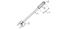
図1には、光導波体1の一方の端部の端面に変換素子2をコーティングし、他方の端部に半導体光源3を配置した光源が示されている。半導体光源3は1次放射の光を光導波体1へ入力する。当該の光は光導波体1のうち変換素子2を有する側の端部から出射されるときに蛍光物質の励起によって少なくとも部分的にルミネセンス変換される(したがって以下では変換素子をルミネセンス変換素子とも称する)。形成された1次放射は蛍光物質により2次放射へ変換され、光導波体からの出射の際に2次放射と重畳されて混合光が形成される。有利には、蛍光物質は母材に埋め込まれている。
FIG. 1 shows a light source in which a
ルミネセンス変換素子2で生じた熱を良好に放出するために、熱伝導性のカバーすなわち熱伝導層4が光導波体に設けられる。当該の熱伝導層4は、ルミネセンス変換素子2で生じた熱を効率的に放出できるよう、特にルミネセンス変換素子2に直接に接触している。熱伝導層4は効率的な放熱にとって必要な長さLだけ光導波体の上部に延在していればよい。この実施例では、熱伝導層4は金またはアルミニウムから成る金属層として構成されている。
In order to satisfactorily release the heat generated in the
図2には、良好な放熱のために熱伝導性のカバーすなわち熱伝導層4の設けられた光導波体1およびその端部のルミネセンス変換素子2が示されている。当該のカバーはルミネセンス変換素子2に直接に接触している。この実施例では、熱伝導層4は金またはアルミニウムから成る金属層として構成されている。ルミネセンス変換素子2とは反対側の端部にカップリングコネクタ5、特にFCコネクタまたはSMCコネクタなどの標準コネクタを設けることにより、複数の短い光導波体を結合して標準の光導波体とすることができる。
FIG. 2 shows an optical waveguide 1 provided with a thermally conductive cover, that is, a thermally conductive layer 4 and a
図1に示されているように、熱伝導層は設定された長さLだけ設けられればよく、それ以上の長さの層が設けられても放熱性はめざましくは向上しない。熱伝導性のカバーの最適な長さは熱伝導層材料、熱伝導層の厚さおよび形成される1次放射の波長に基づいて定まる。また、熱伝導性のカバーの寸法はルミネセンス変換素子での変換効率によっても変化する。 As shown in FIG. 1, the heat conductive layer only needs to be provided for a set length L, and even if a layer having a longer length is provided, the heat dissipation performance is not significantly improved. The optimum length of the thermally conductive cover is determined based on the thermally conductive layer material, the thickness of the thermally conductive layer, and the wavelength of the primary radiation that is formed. Moreover, the dimension of a heat conductive cover changes also with the conversion efficiency in a luminescence conversion element.
熱伝導層4の寸法を設計する際には、ルミネセンス変換素子が変換のタイプと半導体光源の励起波長とに基づく100%の初期効率を有し、これにより加熱されることを考慮しなければならない。当該の熱は熱伝導性の材料の冷却によって捕えられ、放出される。そうでないと、加熱された蛍光物質の効率が低下し、加熱のさらなる増大が生じてこれが加速されていく。これはいわゆるポジティブフィードバック(正帰還)である。 When designing the dimensions of the heat conducting layer 4, it must be considered that the luminescence conversion element has an initial efficiency of 100% based on the type of conversion and the excitation wavelength of the semiconductor light source and is thereby heated. Don't be. The heat is captured and released by cooling the thermally conductive material. Otherwise, the efficiency of the heated phosphor will be reduced and further heating will be generated and accelerated. This is so-called positive feedback.
図3〜図5に示されている熱伝導層の寸法設計のためのパラメータ曲線から、マルチモード光導波体のファセット面に配置されたルミネセンス変換素子が種々のパラメータのもとで加熱される様子が見て取れる。パラメータとして、光導波体の直径、熱伝導性のカバーの厚さおよび材料、ならびに、ルミネセンス変換素子の変換効率が用いられている。ここでの1次放射は光出力50mWの青色レーザーの光であり、これが完全に光導波体へ入力されるものとする。図示されているのは、励起波長390nmで光出力のうち40%が熱損失へ変換されるケースと、励起波長440nmで光出力のうち15%が熱損失へ変換されるケースとの2つである。効率はそれぞれ60%および85%となる。 From the parameter curves for the dimensional design of the heat conducting layer shown in FIGS. 3 to 5, the luminescence conversion elements arranged on the facet surface of the multimode optical waveguide are heated under various parameters. You can see the situation. As parameters, the diameter of the optical waveguide, the thickness and material of the thermally conductive cover, and the conversion efficiency of the luminescence conversion element are used. Here, the primary radiation is blue laser light having an optical output of 50 mW, which is completely input to the optical waveguide. There are two cases where 40% of the optical output is converted to heat loss at an excitation wavelength of 390 nm, and 15% of the optical output is converted to heat loss at an excitation wavelength of 440 nm. is there. The efficiency is 60% and 85%, respectively.
図4には、コア直径100μm,全径220μmの光導波体が示されており、図5にはコア直径100μm,全径110μmの光導波体が示されている。 FIG. 4 shows an optical waveguide having a core diameter of 100 μm and a total diameter of 220 μm, and FIG. 5 shows an optical waveguide having a core diameter of 100 μm and a total diameter of 110 μm.
変換効率を不要に損なわないようにするために、ルミネセンス変換素子の温度は100℃を超えてはならない。図3〜図5の曲線から、全径220μmまたは全径110μmの光導波体のどちらにおいても、市販入手可能な厚さ17μmの金メタライゼーションまたは厚さ30μmのアルミニウムメタライゼーションにより、波長440nmの場合にルミネセンス変換素子の効率的な冷却が充分に達成されることが見て取れる。励起波長390nmで変換効率60%のときには、金またはアルミニウムのメタライゼーションの厚さを光導波体の直径に基づいて著しく大きくしなければならない。ルミネセンス変換素子の温度が100℃未満でありかつ室温のもとにあるときメタライゼーションの厚さの単位はμmである。次の表にこれらの数値の関係を挙げる。 In order not to unnecessarily impair the conversion efficiency, the temperature of the luminescence conversion element must not exceed 100 ° C. From the curves in FIGS. 3 to 5, in the case of a wavelength of 440 nm with a commercially available gold metallization having a thickness of 17 μm or an aluminum metallization having a thickness of 30 μm in either an optical waveguide having a total diameter of 220 μm or a total diameter of 110 μm. It can be seen that efficient cooling of the luminescence conversion element is sufficiently achieved. At an excitation wavelength of 390 nm and a conversion efficiency of 60%, the gold or aluminum metallization thickness must be significantly increased based on the diameter of the optical waveguide. When the temperature of the luminescence conversion element is less than 100 ° C. and at room temperature, the unit of thickness of the metallization is μm. The following table lists these numerical values.

ルミネセンス変換素子の温度は、光導波体の端面またはファセット面から光導波体の主軸方向に対して平行に測定される熱伝導層の長さLすなわちアルミニウムのカバーでの30mm,金のカバーでの20mmには無関係である。ここから、光導波体の一部をごく短く金属で覆うのみで充分であることがわかる。 The temperature of the luminescence conversion element is the length L of the heat conductive layer measured parallel to the optical waveguide main axis direction from the end face or facet of the optical waveguide, that is, 30 mm for the aluminum cover, and for the gold cover. This is unrelated to 20 mm. From this it can be seen that it is sufficient to cover a portion of the optical waveguide with a very short metal.
短いファイバ部材はカップリングコネクタ5,特に図2に示されているようなFCコネクタまたはFMCコネクタなどの標準コネクタを介して、標準光導波体へ結合することができる。これにより光源全体にかかるコストを小さく保持することができる。
The short fiber member can be coupled to a standard optical waveguide via a
例えば、金から成るかまたは主として金を含む熱伝導層4の長さLは少なくとも20mmであり多くとも30mmである。同様に、アルミニウムから成るかまたは主としてアルミニウムを含む熱伝導層4の長さLは少なくとも30mmであり多くとも40mmである。カバーの厚さは上掲の表または図4,図5に相応に選定される。 For example, the length L of the heat conducting layer 4 made of gold or mainly containing gold is at least 20 mm and at most 30 mm. Similarly, the length L of the heat conducting layer 4 made of aluminum or mainly containing aluminum is at least 30 mm and at most 40 mm. The thickness of the cover is selected corresponding to the above table or FIG. 4 and FIG.
有利には、熱伝導層4はパターニングされた状態で光導波体に被着される。つまり、熱伝導層4は、さしあたり光導波体の全体にコーティングされてその後パターニングされるのではなく、所望の長さLおよび所望の厚さを有する状態で直接に被着されるのである。 Advantageously, the heat conducting layer 4 is applied to the optical waveguide in a patterned state. That is, the heat conductive layer 4 is not directly coated on the entire optical waveguide and then patterned, but is directly applied in a state having a desired length L and a desired thickness.
図6に関連して、複数の光導波体(ここでは3つの光導波体)を同一の半導体光源3に光学的に接続する実施例を説明する。各光導波体の端面にはルミネセンス変換素子2が配置されている。ルミネセンス変換素子2はそれぞれ異なる色の光を放射する各別の変換素子であってよい。また、各光導波体は所定の長さLまで熱伝導層4によってカバーされている。各光導波体は有利には全長にわたってはコーティングされない。このようにして各光導波体は少なくとも熱伝導層4の設けられていない領域において特にフレキシブルとなる。
An embodiment in which a plurality of optical waveguides (here, three optical waveguides) are optically connected to the same
本願は独国出願第102007046611.2号の優先権を主張するものであり、その開示内容は引用により本願に含まれるものとする。 This application claims the priority of German application No. 100070466611.2, the disclosure of which is hereby incorporated by reference.
本発明は前述した実施例に限定されない。本発明の全ての特徴は、それが特許請求の範囲ないし発明の詳細な説明に明示的に記載されていなくても、個別にまたは任意に組み合わせて本発明の対象となりうる。 The present invention is not limited to the embodiments described above. All features of the present invention may be subject to the present invention individually or in any combination, even if not explicitly stated in the claims or in the detailed description of the invention.
1 光導波体、 2 変換素子、 3 半導体光源、 4 熱伝導層、 5 カップリングコネクタ DESCRIPTION OF SYMBOLS 1 Optical waveguide body, 2 Conversion element, 3 Semiconductor light source, 4 Thermal conductive layer, 5 Coupling connector
Claims (15)
該少なくとも1つの光導波体の一方の端部に変換素子(2)が配置されており、該少なくとも1つの光導波体の他方の端部に前記半導体光源(3)が配置されている
ことを特徴とする光源。 A semiconductor light source (3) and at least one optical waveguide (1);
The conversion element (2) is disposed at one end of the at least one optical waveguide, and the semiconductor light source (3) is disposed at the other end of the at least one optical waveguide. Characteristic light source.
Applications Claiming Priority (1)
| Application Number | Priority Date | Filing Date | Title |
|---|---|---|---|
| DE102007046611A DE102007046611A1 (en) | 2007-09-28 | 2007-09-28 | Light source with conversion element and optical waveguide, method for producing the light source and their use |
Publications (2)
| Publication Number | Publication Date |
|---|---|
| JP2009088531A true JP2009088531A (en) | 2009-04-23 |
| JP2009088531A5 JP2009088531A5 (en) | 2011-10-13 |
Family
ID=40070939
Family Applications (1)
| Application Number | Title | Priority Date | Filing Date |
|---|---|---|---|
| JP2008250988A Pending JP2009088531A (en) | 2007-09-28 | 2008-09-29 | Light source |
Country Status (4)
| Country | Link |
|---|---|
| US (1) | US7706053B2 (en) |
| EP (1) | EP2042898B1 (en) |
| JP (1) | JP2009088531A (en) |
| DE (1) | DE102007046611A1 (en) |
Cited By (2)
| Publication number | Priority date | Publication date | Assignee | Title |
|---|---|---|---|---|
| JP2011029432A (en) * | 2009-07-27 | 2011-02-10 | Sharp Corp | Light-emitting device and lighting device with the same |
| WO2014013923A1 (en) * | 2012-07-17 | 2014-01-23 | 東芝ライテック株式会社 | Solid-state lighting device |
Families Citing this family (11)
| Publication number | Priority date | Publication date | Assignee | Title |
|---|---|---|---|---|
| EA035147B1 (en) * | 2010-07-08 | 2020-05-06 | Баксалта Инкорпорейтид | Method of producing recombinant adamts13 in cell culture |
| US9090315B1 (en) * | 2010-11-23 | 2015-07-28 | Piedra—Sombra Corporation, Inc. | Optical energy transfer and conversion system |
| DE102011080179A1 (en) * | 2011-08-01 | 2013-02-07 | Osram Ag | Wavelength conversion body and method for its production |
| DE102011085385A1 (en) * | 2011-10-28 | 2013-05-02 | Bayerische Motoren Werke Aktiengesellschaft | Lighting device for a motor vehicle |
| US9850711B2 (en) | 2011-11-23 | 2017-12-26 | Stone Aerospace, Inc. | Autonomous laser-powered vehicle |
| EP2840302B1 (en) * | 2011-12-20 | 2019-01-30 | Stanley Electric Co., Ltd. | Light emitting device, vehicle light and vehicle |
| DE102014100723A1 (en) * | 2014-01-23 | 2015-07-23 | Hella Kgaa Hueck & Co. | Lighting device for vehicles |
| US9873495B2 (en) | 2014-12-19 | 2018-01-23 | Stone Aerospace, Inc. | System and method for automated rendezvous, docking and capture of autonomous underwater vehicles |
| US10081446B2 (en) | 2015-03-11 | 2018-09-25 | William C. Stone | System for emergency crew return and down-mass from orbit |
| EP3279556B1 (en) | 2016-08-06 | 2022-09-28 | biolitec Unternehmensbeteiligungs II AG | Fiber optic light source |
| US11493233B2 (en) | 2016-09-26 | 2022-11-08 | Stone Aerospace, Inc. | Direct high voltage water heater |
Citations (2)
| Publication number | Priority date | Publication date | Assignee | Title |
|---|---|---|---|---|
| WO2006038502A1 (en) * | 2004-10-01 | 2006-04-13 | Nichia Corporation | Light-emitting device |
| JP2007027688A (en) * | 2005-06-13 | 2007-02-01 | Nichia Chem Ind Ltd | Light emitting device |
Family Cites Families (6)
| Publication number | Priority date | Publication date | Assignee | Title |
|---|---|---|---|---|
| JPH04507299A (en) * | 1989-02-01 | 1992-12-17 | ザ ボード オブ トラスティーズ オブ ザ リーランド スタンフォード ジュニア ユニバーシティ | Nonlinear optical oscillator and method for controlling ferroelectric polarization region of semiconductor |
| CN100394298C (en) * | 1995-06-02 | 2008-06-11 | 松下电器产业株式会社 | Optical element, laser light source and laser device and method of mfg. such optical device |
| DE29724847U1 (en) * | 1996-06-26 | 2004-09-30 | Osram Opto Semiconductors Gmbh | Light-emitting semiconductor component with luminescence conversion element |
| DE19638667C2 (en) * | 1996-09-20 | 2001-05-17 | Osram Opto Semiconductors Gmbh | Mixed-color light-emitting semiconductor component with luminescence conversion element |
| US6921920B2 (en) | 2001-08-31 | 2005-07-26 | Smith & Nephew, Inc. | Solid-state light source |
| JP4689190B2 (en) * | 2004-05-18 | 2011-05-25 | オリンパス株式会社 | Endoscope device and endoscope adapter |
-
2007
- 2007-09-28 DE DE102007046611A patent/DE102007046611A1/en not_active Withdrawn
-
2008
- 2008-09-16 EP EP08164447A patent/EP2042898B1/en active Active
- 2008-09-19 US US12/233,833 patent/US7706053B2/en active Active
- 2008-09-29 JP JP2008250988A patent/JP2009088531A/en active Pending
Patent Citations (2)
| Publication number | Priority date | Publication date | Assignee | Title |
|---|---|---|---|---|
| WO2006038502A1 (en) * | 2004-10-01 | 2006-04-13 | Nichia Corporation | Light-emitting device |
| JP2007027688A (en) * | 2005-06-13 | 2007-02-01 | Nichia Chem Ind Ltd | Light emitting device |
Cited By (2)
| Publication number | Priority date | Publication date | Assignee | Title |
|---|---|---|---|---|
| JP2011029432A (en) * | 2009-07-27 | 2011-02-10 | Sharp Corp | Light-emitting device and lighting device with the same |
| WO2014013923A1 (en) * | 2012-07-17 | 2014-01-23 | 東芝ライテック株式会社 | Solid-state lighting device |
Also Published As
| Publication number | Publication date |
|---|---|
| US7706053B2 (en) | 2010-04-27 |
| EP2042898B1 (en) | 2013-03-13 |
| US20090086309A1 (en) | 2009-04-02 |
| DE102007046611A1 (en) | 2009-04-02 |
| EP2042898A1 (en) | 2009-04-01 |
Similar Documents
| Publication | Publication Date | Title |
|---|---|---|
| JP2009088531A (en) | Light source | |
| JP5083592B2 (en) | Optical component, light conversion member, and light emitting device | |
| KR101186388B1 (en) | Light emitting device | |
| US7737457B2 (en) | Phosphor down converting element for an LED package and fabrication method | |
| CN108235720A (en) | For generating the optical device of high-luminance light | |
| WO2017073054A1 (en) | Light emitting device | |
| JP5844484B2 (en) | Conversion member, illumination means, and method of manufacturing conversion member | |
| JP2010541221A (en) | Semiconductor light source with primary radiation source and luminescence conversion element | |
| JP6231112B2 (en) | Ceramic conversion element, optoelectronic semiconductor device, and method of manufacturing ceramic conversion element | |
| TW200822403A (en) | Light-emitting device and method for manufacturing the same | |
| JP2016009761A (en) | Light emitting module | |
| JP2013207049A (en) | Light emitting device using wavelength conversion body | |
| JP2005244075A (en) | Light emitting device | |
| JP6457099B2 (en) | Wavelength conversion member and light emitting device | |
| JP6804448B2 (en) | Luminescent device | |
| EP3396232A1 (en) | Light-emitting element and illumination device | |
| US20140264359A1 (en) | Lightweight self-cooling light sources | |
| JP2008521238A (en) | Light emitting device having an inorganic housing | |
| JP2014179231A (en) | Light source device and lighting device | |
| WO2015195820A1 (en) | Method of making a ceramic wavelength converter assembly | |
| CN108884973A (en) | semiconductor light source | |
| JP2009038260A (en) | Light emitting element | |
| JP2017215568A (en) | Wavelength conversion element, light source device, and image projection device | |
| US20140166902A1 (en) | Wavelength Conversion Body And Method For Manufacturing Same | |
| JPWO2017119022A1 (en) | Light emitting device |
Legal Events
| Date | Code | Title | Description |
|---|---|---|---|
| RD04 | Notification of resignation of power of attorney |
Free format text: JAPANESE INTERMEDIATE CODE: A7424 Effective date: 20101227 |
|
| RD04 | Notification of resignation of power of attorney |
Free format text: JAPANESE INTERMEDIATE CODE: A7424 Effective date: 20101228 |
|
| A521 | Request for written amendment filed |
Free format text: JAPANESE INTERMEDIATE CODE: A523 Effective date: 20110830 |
|
| A621 | Written request for application examination |
Free format text: JAPANESE INTERMEDIATE CODE: A621 Effective date: 20110830 |
|
| A977 | Report on retrieval |
Free format text: JAPANESE INTERMEDIATE CODE: A971007 Effective date: 20121107 |
|
| A131 | Notification of reasons for refusal |
Free format text: JAPANESE INTERMEDIATE CODE: A131 Effective date: 20121109 |
|
| A521 | Request for written amendment filed |
Free format text: JAPANESE INTERMEDIATE CODE: A523 Effective date: 20130204 |
|
| A02 | Decision of refusal |
Free format text: JAPANESE INTERMEDIATE CODE: A02 Effective date: 20130708 |