JP2009081400A - Shield structure of electronic device terminal - Google Patents
Shield structure of electronic device terminal Download PDFInfo
- Publication number
- JP2009081400A JP2009081400A JP2007251421A JP2007251421A JP2009081400A JP 2009081400 A JP2009081400 A JP 2009081400A JP 2007251421 A JP2007251421 A JP 2007251421A JP 2007251421 A JP2007251421 A JP 2007251421A JP 2009081400 A JP2009081400 A JP 2009081400A
- Authority
- JP
- Japan
- Prior art keywords
- shield
- electronic device
- sheet
- conductive adhesive
- shield structure
- Prior art date
- Legal status (The legal status is an assumption and is not a legal conclusion. Google has not performed a legal analysis and makes no representation as to the accuracy of the status listed.)
- Pending
Links
Images


Landscapes
- Shielding Devices Or Components To Electric Or Magnetic Fields (AREA)
- Telephone Set Structure (AREA)
Abstract
Description
本発明は、携帯電話機、PHS(Personal Handy−phone System)等の携帯型無線通信機器に使用される電子機器端末のシールド構造に関するものである。 The present invention relates to a shield structure for an electronic device terminal used in a portable wireless communication device such as a mobile phone or a PHS (Personal Handy-phone System).
従来の携帯型無線通信機器は、図8及び図9に示すような電気的シールド構造を有する(例えば、特許文献1参照)。図8は従来の携帯型無線通信機器のシールド構造の断面図であり、図9は分解斜視図である。 A conventional portable wireless communication device has an electrical shield structure as shown in FIGS. 8 and 9 (see, for example, Patent Document 1). FIG. 8 is a sectional view of a shield structure of a conventional portable wireless communication device, and FIG. 9 is an exploded perspective view.
図8及び図9において、1は配線基板、2及び3は配線基板1上に搭載された電子部品、4は配線基板1に接合されたシールドフレーム、5はシールドフレーム4に嵌合し複数の電子部品2、3を一括して閉塞するシールドカバーを示す。
8 and 9, 1 is a wiring board, 2 and 3 are electronic components mounted on the
高周波回路占有領域を閉塞するシールドフレーム4及びシールドフレーム5は、板金材料により形成されている。薄型軽量化が要求される携帯型無線通信機器においては、図8及び図9に示すとおり、電子部品2、3のように部品の高さに違いがある場合には、シールドフレーム4及びシールドフレーム5は、高周波回路占有領域内の最高背部品である電子部品2の領域に開口穴4a、5aが設けられる。
The
しかしながら、上記従来の電子機器端末のシールド構造では、携帯型無線通信機器の薄型軽量化を優先してシールドフレーム4及びシールドフレーム5に開口穴4a、5aを設けることによりシールドの効果が不十分であるという問題があった。
However, in the shield structure of the above-described conventional electronic device terminal, the shield effect is insufficient by providing the opening holes 4a and 5a in the
また、シールドの効果を優先して開口穴4a、5aを設けない場合には、薄型軽量化を阻害するという問題があった。さらに、開口穴4a、5aを設けずにシールドカバー5の天面に段差を設けて薄型化を図る場合には、板金材料の加工が困難であるという問題があった。
In addition, when the opening holes 4a and 5a are not provided by giving priority to the effect of the shield, there is a problem that the reduction in thickness and weight is hindered. Furthermore, when a step is provided on the top surface of the
本発明は、上記の課題を解決するためのものであり、薄型軽量化、省スペース化を図るとともに、電気的シールドの効果を向上できる電子機器端末のシールド構造を提供することを目的としている。 An object of the present invention is to provide a shield structure for an electronic device terminal that can reduce the thickness and weight, save space, and improve the effect of an electrical shield.
本発明に係る電子機器端末のシールド構造は、基板上に設けられた電子部品の外表面及び周囲の基板面を覆う導電層と、導電層と電子部品との間において電子部品の外表面と接着する非導電性粘着層と、導電層と電子部品周囲の基板面とを接着し、導電層と基板上の接地端子とを接続する導電性粘着層とを備えるものである。 The shield structure of the electronic device terminal according to the present invention includes a conductive layer covering the outer surface of the electronic component and the surrounding substrate surface provided on the substrate, and the outer surface of the electronic component bonded between the conductive layer and the electronic component. A non-conductive adhesive layer that adheres to the conductive layer and the substrate surface around the electronic component, and a conductive adhesive layer that connects the conductive layer and the ground terminal on the substrate.
本発明によれば、基板上に設けられた電子部品をシート状の非導電性粘着層を介してシート状の金属層で覆い、シート状の金属層をシート状の導電性粘着層を介して基板に接着して接地端子と電気的に接続することにより、高さの異なる電子部品を覆う場合であっても、各電子部品の形状に追従した形で確実にかつ容易に電気的にシールドできる。また、シールド部品に開口部を設けることなく、薄型軽量化を図ることができる。 According to the present invention, an electronic component provided on a substrate is covered with a sheet-like metal layer via a sheet-like non-conductive adhesive layer, and the sheet-like metal layer is covered via a sheet-like conductive adhesive layer. Even when covering electronic components with different heights by adhering to the substrate and electrically connecting to the ground terminal, it can be reliably and easily electrically shielded in a form that follows the shape of each electronic component. . Further, it is possible to reduce the thickness and weight without providing an opening in the shield component.
以下、本発明に係る電子機器端末のシールド構造の各種実施の形態について、図面に基づいて説明する。
実施の形態1.
図1、図2及び図3は、本発明の実施の形態1による電子機器端末のシールド構造の構成を示す概略図である。図1は外観斜視図であり、図2は図1のA−Aにおける矢視断面図であり、図3は図1のB−Bにおける矢視断面図である。
Hereinafter, various embodiments of a shield structure for an electronic device terminal according to the present invention will be described with reference to the drawings.
1, 2 and 3 are schematic views showing the configuration of the shield structure of the electronic device terminal according to
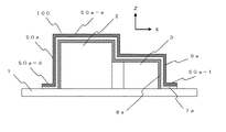
図2乃至図3において、100は電子部品2、3を閉塞するシート状シールド部品を示し、6a、6b、6cは電気的シールド機能を有するシート状の金属層、7a、7b、7cはシート状の導電性粘着層、8a、8b、8cはシート状の非導電性粘着層を示す。
2 to 3,
シート状シールド部品100は、電子部品2、3とは非導電性粘着層8a、8b、8cを介して金属層6a、6b、6cで覆って接着し、電子部品2、3を閉塞する。配線基板1とは導電性粘着層7a、7b、7cを介して接着し、配線基板1上の接地端子と金属層6を電気的に接続する。
The sheet-
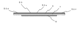
図4は、シート状シールド部品100を形成するためのシールド用シート50の断面図である。図4において、シールド用シート50は、金属層6、導電性粘着層7及び非導電性粘着層8の三層で構成されている。
FIG. 4 is a cross-sectional view of a
シールド用シート50の中央部50eは、金属層6、導電性粘着層7及び電子部品2、3とを絶縁して接着するための非導電性粘着層8を設けた三層からなり、端部50d、50fは配線基板1と金属層6を電気的に接続して接着するため非導電性粘着層8を削除した二層からなる。
The central portion 50e of the
次に、シールド用シート50からシート状シールド部品100を形成する方法について説明する。まず、図1に示す電子部品2、3のXY面となる天面及びYZ面側の両側面を、シールド用シート50aの中央部50a−eで貼り付けて覆い、端部50a−d、50a−fを配線基板1に貼り付ける(図2参照)。
Next, a method for forming the sheet-
続いて、電子部品2、3のXZ面側である他方の両側面をそれぞれ、シールド用シート50bの中央部50b−eとシールド用シート50cの中央部50c−eで貼り付けて覆い、シールド用シート50b、50cの一方の端部50b−d、50c−dで電子部品2、3の天面及び側面に貼り付けたシールド用シート50aの中央部50a−eの金属層6a側端部に貼り付けて電気的に接続するまた、シールド用シート50b、50cの他方の端部50b−f、50c−fを配線基板1に貼り付ける(図3参照)。
Subsequently, the other side surfaces on the XZ plane side of the
上記のように、配線基板1上の電子部品2、3の全表面を、露出する部分がないようにシールド用シート50a、50b、50cで覆い、シート状シールド部品100が形成される。配線基板1への貼り付けでは、端部50b−f、50c−f、50a−d、もしくは50a−fのいずれかが配線基板1上の接地端子と金属層6を電気的に接続する。
As described above, the entire surfaces of the
以上のように、本実施の形態1では、配線基板1上に設けられた電子部品2、3をシート状の非導電性粘着層8a、8b、8cを介してシート状の金属層6a、6b、6cで覆い、シート状の金属層6a、6b、6cをシート状の導電性粘着層7a、7b、7cを介して配線基板1に接着して接地端子と電気的に接続するようにしたので、高さの異なる電子部品を覆う場合であっても、各電子部品の形状に追従した形で確実にかつ容易に電気的にシールドできる。また、シールド部品に開口部を設けることなく、薄型軽量化を図ることができる。
As described above, in the first embodiment, the
なお、本実施の形態1では、シート状シールド部品100を形成するために、金属層6、導電性粘着層7及び非導電性粘着層8の三層からなるシールド用シート50を用いた場合について説明したが、図5に示すシールド用シート51のように、中央部51eが金属層6及び非導電性粘着層8の二層からなるシールド用シートを用いてもよい。
In the first embodiment, in order to form the sheet-
図6及び図7に、シールド用シート51を用いて形成したシート状シールド部品101の断面図を示す。この場合、シート状シールド部品100に比べ、更なる薄型軽量化を実現できる。
6 and 7 are cross-sectional views of the sheet-like shield component 101 formed using the
また、本実施の形態1では、複数の電子部品2、3を一体的に覆ってシート状シールド部品100を形成したが、別個に覆って形成してもよい。この場合は、更に各電子部品に追従した形状でシート状シールド部品を形成することができ、省スペース化を図ることができる。
In the first embodiment, the sheet-
1 配線基板
2、3 電子部品
6a、6b、6c 金属層
7a、7b、7c 導電性粘着層
8a、8b、8c 非導電性粘着層
100、101 シート状シールド部品
DESCRIPTION OF
Claims (4)
この導電層と前記電子部品との間において前記電子部品の外表面と接着する非導電性粘着層と、
前記導電層と前記電子部品周囲の基板面とを接着し、前記導電層と前記基板上の接地端子とを接続する導電性粘着層とを備える電子機器端末のシールド構造。 A conductive layer covering the outer surface of the electronic component provided on the substrate and the surrounding substrate surface;
A non-conductive adhesive layer that adheres to the outer surface of the electronic component between the conductive layer and the electronic component;
A shield structure for an electronic device terminal, comprising: a conductive adhesive layer that bonds the conductive layer and a substrate surface around the electronic component and connects the conductive layer and a ground terminal on the substrate.
Priority Applications (1)
| Application Number | Priority Date | Filing Date | Title |
|---|---|---|---|
| JP2007251421A JP2009081400A (en) | 2007-09-27 | 2007-09-27 | Shield structure of electronic device terminal |
Applications Claiming Priority (1)
| Application Number | Priority Date | Filing Date | Title |
|---|---|---|---|
| JP2007251421A JP2009081400A (en) | 2007-09-27 | 2007-09-27 | Shield structure of electronic device terminal |
Publications (1)
| Publication Number | Publication Date |
|---|---|
| JP2009081400A true JP2009081400A (en) | 2009-04-16 |
Family
ID=40655894
Family Applications (1)
| Application Number | Title | Priority Date | Filing Date |
|---|---|---|---|
| JP2007251421A Pending JP2009081400A (en) | 2007-09-27 | 2007-09-27 | Shield structure of electronic device terminal |
Country Status (1)
| Country | Link |
|---|---|
| JP (1) | JP2009081400A (en) |
Cited By (5)
| Publication number | Priority date | Publication date | Assignee | Title |
|---|---|---|---|---|
| WO2010113961A1 (en) | 2009-03-30 | 2010-10-07 | 株式会社資生堂 | Method for applying external skin preparation, method for evaluating application by the method, device for evaluating the application and program for evaluating the application |
| WO2012035864A1 (en) | 2010-09-17 | 2012-03-22 | 株式会社資生堂 | Evaluation method of ultraviolet radiation protective effect, evaluation device, and recording medium |
| JP2013021671A (en) * | 2011-07-13 | 2013-01-31 | Lg Electronics Inc | Mobile terminal |
| JP2015065343A (en) * | 2013-09-25 | 2015-04-09 | タツタ電線株式会社 | Shield housing body, printed circuit board, electronic apparatus and method for manufacturing shield housing body |
| WO2015083491A1 (en) * | 2013-12-03 | 2015-06-11 | 東洋インキScホールディングス株式会社 | Electronic element and sheet material |
-
2007
- 2007-09-27 JP JP2007251421A patent/JP2009081400A/en active Pending
Cited By (10)
| Publication number | Priority date | Publication date | Assignee | Title |
|---|---|---|---|---|
| WO2010113961A1 (en) | 2009-03-30 | 2010-10-07 | 株式会社資生堂 | Method for applying external skin preparation, method for evaluating application by the method, device for evaluating the application and program for evaluating the application |
| WO2012035864A1 (en) | 2010-09-17 | 2012-03-22 | 株式会社資生堂 | Evaluation method of ultraviolet radiation protective effect, evaluation device, and recording medium |
| JP2013021671A (en) * | 2011-07-13 | 2013-01-31 | Lg Electronics Inc | Mobile terminal |
| US8976540B2 (en) | 2011-07-13 | 2015-03-10 | Lg Electronics Inc. | Mobile terminal |
| JP2015065343A (en) * | 2013-09-25 | 2015-04-09 | タツタ電線株式会社 | Shield housing body, printed circuit board, electronic apparatus and method for manufacturing shield housing body |
| WO2015083491A1 (en) * | 2013-12-03 | 2015-06-11 | 東洋インキScホールディングス株式会社 | Electronic element and sheet material |
| JP2015130484A (en) * | 2013-12-03 | 2015-07-16 | 東洋インキScホールディングス株式会社 | Electronic element and sheet material |
| CN105794331A (en) * | 2013-12-03 | 2016-07-20 | 东洋油墨Sc控股株式会社 | Electronic element and sheet material |
| KR20180059952A (en) * | 2013-12-03 | 2018-06-05 | 토요잉크Sc홀딩스주식회사 | Electronic element and sheet material |
| KR102150258B1 (en) | 2013-12-03 | 2020-09-01 | 토요잉크Sc홀딩스주식회사 | Electronic element and sheet material |
Similar Documents
| Publication | Publication Date | Title |
|---|---|---|
| US7904123B2 (en) | Shield case and MEMS microphone having it | |
| US8890265B2 (en) | Semiconductor device and microphone | |
| US20180146302A1 (en) | Mems microphone package structure and method for manufacturing the mems microphone package structures | |
| EP3307036B1 (en) | Mobile terminal and heat dissipation shielding structure | |
| US9876273B2 (en) | Electronic device having antenna on grounded speaker box | |
| US20170064458A1 (en) | Mems microphone package structure having a non-planar substrate | |
| KR20130055661A (en) | Portable electronic device | |
| US9345134B2 (en) | Printed wiring board | |
| JP2009065388A (en) | Wireless communication device and antenna device | |
| CN105357616B (en) | Micro-electro-mechanical microphone packaging structure with three-dimensional substrate | |
| KR100903373B1 (en) | Loop Antenna And Manufacturing Method Of The Same | |
| US8155366B2 (en) | Transducer package with interior support frame | |
| JP2009081400A (en) | Shield structure of electronic device terminal | |
| WO2021185237A1 (en) | Circuit board assembly and electronic device | |
| CN104125761A (en) | Shield apparatus for electronic device | |
| US20100316246A1 (en) | Speaker device for portable terminal | |
| JP2010056180A (en) | Circuit module | |
| JP2006147917A (en) | Radio terminal and shielding structure thereof | |
| JP2011024022A (en) | Mobile walkie-talkie | |
| WO2012096354A1 (en) | High-frequency module | |
| US8884164B2 (en) | Circuit board assembly with flexible printed circuit board and reinforcing plate | |
| WO2017006614A1 (en) | High frequency module | |
| JP2007199049A (en) | Semiconductor device | |
| US8130506B2 (en) | Sensor module | |
| JP2010192670A (en) | Semiconductor package and method of manufacturing the same |