JP2009076870A - Plasma reactor with reduced electrical skew using electrical bypass element - Google Patents
Plasma reactor with reduced electrical skew using electrical bypass element Download PDFInfo
- Publication number
- JP2009076870A JP2009076870A JP2008192135A JP2008192135A JP2009076870A JP 2009076870 A JP2009076870 A JP 2009076870A JP 2008192135 A JP2008192135 A JP 2008192135A JP 2008192135 A JP2008192135 A JP 2008192135A JP 2009076870 A JP2009076870 A JP 2009076870A
- Authority
- JP
- Japan
- Prior art keywords
- sidewall
- pedestal
- reactor
- slit valve
- axial
- Prior art date
- Legal status (The legal status is an assumption and is not a legal conclusion. Google has not performed a legal analysis and makes no representation as to the accuracy of the status listed.)
- Withdrawn
Links
- NJPPVKZQTLUDBO-UHFFFAOYSA-N novaluron Chemical compound C1=C(Cl)C(OC(F)(F)C(OC(F)(F)F)F)=CC=C1NC(=O)NC(=O)C1=C(F)C=CC=C1F NJPPVKZQTLUDBO-UHFFFAOYSA-N 0.000 claims abstract description 49
- 238000005086 pumping Methods 0.000 claims abstract description 26
- 238000000034 method Methods 0.000 claims description 18
- 230000008569 process Effects 0.000 claims description 17
- 230000008878 coupling Effects 0.000 claims description 9
- 238000010168 coupling process Methods 0.000 claims description 9
- 238000005859 coupling reaction Methods 0.000 claims description 9
- 230000002093 peripheral effect Effects 0.000 claims description 7
- 235000012431 wafers Nutrition 0.000 description 27
- 239000004020 conductor Substances 0.000 description 12
- 230000005684 electric field Effects 0.000 description 9
- 239000002826 coolant Substances 0.000 description 4
- 239000004065 semiconductor Substances 0.000 description 4
- 238000001020 plasma etching Methods 0.000 description 2
- 238000001636 atomic emission spectroscopy Methods 0.000 description 1
- 230000004323 axial length Effects 0.000 description 1
- 238000011109 contamination Methods 0.000 description 1
- 238000005137 deposition process Methods 0.000 description 1
- 239000003989 dielectric material Substances 0.000 description 1
- 238000007654 immersion Methods 0.000 description 1
- 238000002347 injection Methods 0.000 description 1
- 239000007924 injection Substances 0.000 description 1
- 239000012212 insulator Substances 0.000 description 1
- 238000005468 ion implantation Methods 0.000 description 1
- 230000007246 mechanism Effects 0.000 description 1
- 229910052751 metal Inorganic materials 0.000 description 1
- 239000002184 metal Substances 0.000 description 1
- 150000002739 metals Chemical class 0.000 description 1
- 230000003287 optical effect Effects 0.000 description 1
- 230000000737 periodic effect Effects 0.000 description 1
- 230000035699 permeability Effects 0.000 description 1
Images


Classifications
-
- H—ELECTRICITY
- H01—ELECTRIC ELEMENTS
- H01J—ELECTRIC DISCHARGE TUBES OR DISCHARGE LAMPS
- H01J37/00—Discharge tubes with provision for introducing objects or material to be exposed to the discharge, e.g. for the purpose of examination or processing thereof
- H01J37/02—Details
- H01J37/16—Vessels; Containers
-
- H—ELECTRICITY
- H01—ELECTRIC ELEMENTS
- H01L—SEMICONDUCTOR DEVICES NOT COVERED BY CLASS H10
- H01L21/00—Processes or apparatus adapted for the manufacture or treatment of semiconductor or solid state devices or of parts thereof
- H01L21/02—Manufacture or treatment of semiconductor devices or of parts thereof
- H01L21/04—Manufacture or treatment of semiconductor devices or of parts thereof the devices having potential barriers, e.g. a PN junction, depletion layer or carrier concentration layer
- H01L21/18—Manufacture or treatment of semiconductor devices or of parts thereof the devices having potential barriers, e.g. a PN junction, depletion layer or carrier concentration layer the devices having semiconductor bodies comprising elements of Group IV of the Periodic Table or AIIIBV compounds with or without impurities, e.g. doping materials
- H01L21/30—Treatment of semiconductor bodies using processes or apparatus not provided for in groups H01L21/20 - H01L21/26
- H01L21/302—Treatment of semiconductor bodies using processes or apparatus not provided for in groups H01L21/20 - H01L21/26 to change their surface-physical characteristics or shape, e.g. etching, polishing, cutting
- H01L21/306—Chemical or electrical treatment, e.g. electrolytic etching
- H01L21/3065—Plasma etching; Reactive-ion etching
-
- H—ELECTRICITY
- H01—ELECTRIC ELEMENTS
- H01J—ELECTRIC DISCHARGE TUBES OR DISCHARGE LAMPS
- H01J37/00—Discharge tubes with provision for introducing objects or material to be exposed to the discharge, e.g. for the purpose of examination or processing thereof
- H01J37/02—Details
- H01J37/20—Means for supporting or positioning the objects or the material; Means for adjusting diaphragms or lenses associated with the support
-
- H—ELECTRICITY
- H01—ELECTRIC ELEMENTS
- H01J—ELECTRIC DISCHARGE TUBES OR DISCHARGE LAMPS
- H01J37/00—Discharge tubes with provision for introducing objects or material to be exposed to the discharge, e.g. for the purpose of examination or processing thereof
- H01J37/32—Gas-filled discharge tubes
- H01J37/32009—Arrangements for generation of plasma specially adapted for examination or treatment of objects, e.g. plasma sources
- H01J37/32082—Radio frequency generated discharge
-
- H—ELECTRICITY
- H01—ELECTRIC ELEMENTS
- H01J—ELECTRIC DISCHARGE TUBES OR DISCHARGE LAMPS
- H01J37/00—Discharge tubes with provision for introducing objects or material to be exposed to the discharge, e.g. for the purpose of examination or processing thereof
- H01J37/32—Gas-filled discharge tubes
- H01J37/32431—Constructional details of the reactor
- H01J37/32623—Mechanical discharge control means
-
- H—ELECTRICITY
- H01—ELECTRIC ELEMENTS
- H01J—ELECTRIC DISCHARGE TUBES OR DISCHARGE LAMPS
- H01J37/00—Discharge tubes with provision for introducing objects or material to be exposed to the discharge, e.g. for the purpose of examination or processing thereof
- H01J37/32—Gas-filled discharge tubes
- H01J37/32431—Constructional details of the reactor
- H01J37/32697—Electrostatic control
-
- H—ELECTRICITY
- H01—ELECTRIC ELEMENTS
- H01J—ELECTRIC DISCHARGE TUBES OR DISCHARGE LAMPS
- H01J37/00—Discharge tubes with provision for introducing objects or material to be exposed to the discharge, e.g. for the purpose of examination or processing thereof
- H01J37/32—Gas-filled discharge tubes
- H01J37/32431—Constructional details of the reactor
- H01J37/32798—Further details of plasma apparatus not provided for in groups H01J37/3244 - H01J37/32788; special provisions for cleaning or maintenance of the apparatus
- H01J37/32816—Pressure
- H01J37/32834—Exhausting
Landscapes
- Chemical & Material Sciences (AREA)
- Analytical Chemistry (AREA)
- Engineering & Computer Science (AREA)
- Physics & Mathematics (AREA)
- Plasma & Fusion (AREA)
- Condensed Matter Physics & Semiconductors (AREA)
- Computer Hardware Design (AREA)
- Microelectronics & Electronic Packaging (AREA)
- Power Engineering (AREA)
- Manufacturing & Machinery (AREA)
- General Physics & Mathematics (AREA)
- Plasma Technology (AREA)
- Drying Of Semiconductors (AREA)
- Physical Or Chemical Processes And Apparatus (AREA)
Abstract
Description
開示内容は、プラズマリアクタ、特に、半導体ウェハのようなワークピースの処理用のプラズマリアクタに関する。 The disclosure relates to plasma reactors, and in particular to plasma reactors for processing workpieces such as semiconductor wafers.
プラズマリアクタは、例えば、プラズマエッチングプロセス、プラズマ堆積プロセス及びプラズマ浸漬イオン注入等の様々なプラズマプロセスにおける半導体ウェハ等のワークピースの処理に用いられている。半導体装置フィーチャーサイズを減じるには、プラズマリアクタ及びプロセスを改善して、プラズマ処理結果における不均一性を減じる必要がある。例えば、プラズマエッチングプロセスにおいては、ウェハ全体のエッチングレートの半径方向分布は、約5%未満まで良好に減じている。装置フィーチャーサイズは、45nm、更に32nmまで収縮し続けており、プラズマ均一性の更なる改善が望まれている。 Plasma reactors are used to process workpieces such as semiconductor wafers in various plasma processes such as, for example, plasma etching processes, plasma deposition processes, and plasma immersion ion implantation. To reduce semiconductor device feature size, plasma reactors and processes need to be improved to reduce non-uniformities in plasma processing results. For example, in a plasma etching process, the radial distribution of etch rates across the wafer is well reduced to less than about 5%. The device feature size continues to shrink to 45 nm and even 32 nm, and further improvements in plasma uniformity are desired.
本発明の実施形態は、プラズマ均一性の増大した、半導体ワークピース(例えば、ウェハ)を処理するのに用いることのできる装置及び方法に関する。一態様において、プラズマリアクタが、ワークピースの処理のために提供される。リアクタは、円筒形側壁、天井及び床を有する真空チャンバを含む。チャンバのワークピースサポート台座は、台座と側壁の間でポンピングアニュラスを画定しており、ワークピースサポート台座は、床に近接する接地表面を有している。RF電力印加装置は、RF電力を、天井と台座の間で画定されたプロセスゾーンへ結合している。真空ポンプは、床を通してポンピングポートを通してチャンバに結合されている。リアクタは、台座の接地表面と床の間に誘電体要素を更に含む。リアクタはまた、グリルから床までの間隙をあけて、床の上に配置されたポンピングアニュラスに環形導電性グリルも有する。グリルは、側壁から台座の接地表面まで均一な電流路を提供する。グリルは、通常、チャンバの対称軸に対して対称である。 Embodiments of the present invention relate to an apparatus and method that can be used to process semiconductor workpieces (eg, wafers) with increased plasma uniformity. In one aspect, a plasma reactor is provided for workpiece processing. The reactor includes a vacuum chamber having cylindrical side walls, a ceiling and a floor. The workpiece support pedestal of the chamber defines a pumping annulus between the pedestal and the side wall, and the workpiece support pedestal has a grounding surface proximate to the floor. The RF power applicator couples RF power to a process zone defined between the ceiling and the pedestal. A vacuum pump is coupled to the chamber through the pumping port through the floor. The reactor further includes a dielectric element between the pedestal ground surface and the floor. The reactor also has an annular conductive grill in the pumping annulus located on the floor with a gap from the grill to the floor. The grill provides a uniform current path from the side wall to the grounding surface of the pedestal. The grill is usually symmetric with respect to the axis of symmetry of the chamber.
一実施形態において、リアクタは、円筒形側壁の周囲部分を通るスリットバルブ開口部を更に含み、スリットバルブは、円筒形側壁の環形部分内に軸方向に制限されている。少なくとも第1の誘電体リングが、側壁の環形部分の軸方向境界近傍の円筒形側壁に配置されている。列をなす導電性ストラップが、円筒形側壁の環形部分をバイパスする軸方向電流流路を提供する。導電性ストラップは夫々、一対の端部を有し、一方の端部は、環形部分の上の側壁に電気的に接続されており、他方の端部は、環形部分の下の側壁に電気的に接続されている。一実施形態において、ストラップはスリットバルブ開口部へのアクセスを妨げないように迂回されている。 In one embodiment, the reactor further includes a slit valve opening through a peripheral portion of the cylindrical sidewall, the slit valve being axially constrained within the annular portion of the cylindrical sidewall. At least a first dielectric ring is disposed on the cylindrical sidewall near the axial boundary of the annular portion of the sidewall. A row of conductive straps provides an axial current flow path that bypasses the annular portion of the cylindrical sidewall. Each of the conductive straps has a pair of ends, one end electrically connected to the upper sidewall of the annulus and the other end electrically connected to the lower sidewall of the annulus. It is connected to the. In one embodiment, the strap is bypassed so as not to prevent access to the slit valve opening.
一実施形態において、第2の誘電体リングは、円筒形側壁に配置されており、第1の誘電体リングは、側壁の環形部分の上部軸方向境界に近接しており、第2の誘電体リングは、側壁の環形部分の下部軸方向境界に近接している。更なる実施形態において、ストラップは、均一な間隔で、側壁周囲に周期的に間隔をあけており、ストラップは、均一なインダクタンスをRF電流に与えるように構成されている。スリットバルブに近接するストラップは、スリットバルブの周囲を迂回するだけの十分な長さがあり、残りのストラップはこれより短い長さである。 In one embodiment, the second dielectric ring is disposed on the cylindrical sidewall, the first dielectric ring is proximate to the upper axial boundary of the annular portion of the sidewall, and the second dielectric ring The ring is proximate to the lower axial boundary of the annular portion of the sidewall. In further embodiments, the straps are periodically spaced around the sidewalls at uniform intervals, and the straps are configured to provide uniform inductance to the RF current. The strap proximate to the slit valve is long enough to bypass the perimeter of the slit valve and the remaining straps are shorter.
プラズマリアクタの電界における周方向スキューは、プラズマプロセス不均一性を3%未満に減少させる制限因子である可能性があることを知見した。このような周方向スキューは、プラズマリアクタそのものの非対称なフィーチャーに起因する。これら非対称なフィーチャーによって、チャンバ壁と床を通るRF接地リターン電流に不均一性が形成される。このような不均一性は、ウェハ表面の電界分布に反映されて、プロセス不均一性に寄与する。例えば、あるリアクタチャンバにおいては、通常、ポンピングアニュラスの床にある円形開口部であるポンピングポートを通して、そのポンピングアニュラスの下部で、チャンバを排気する。他の例を挙げると、あるリアクタチャンバにおいては、ウェハスリットバルブが提供され、円筒形チャンバ側壁のウェハスリットバルブは、円筒形側壁周囲の約四分の一にわたって延在している。これらのフィーチャーによって、チャンバの導電性床及び壁に不連続性が生じ、RF接地リターン電流を進めて、不均一に分配し、これによって、ウェハ表面で電界に周方向スキューが生じる。これらのスキューは、ウェハのプラズマ処理結果において1%〜2%の不均一性を示す。 It has been found that circumferential skew in the electric field of the plasma reactor can be a limiting factor that reduces plasma process non-uniformity to less than 3%. Such circumferential skew is due to asymmetric features of the plasma reactor itself. These asymmetric features create non-uniformities in the RF ground return current through the chamber walls and floor. Such non-uniformity is reflected in the electric field distribution on the wafer surface and contributes to process non-uniformity. For example, in some reactor chambers, the chamber is typically evacuated at the bottom of the pumping annulus through a pumping port, which is a circular opening in the floor of the pumping annulus. As another example, in some reactor chambers, a wafer slit valve is provided, with the wafer slit valve on the cylindrical chamber sidewall extending about a quarter of the circumference of the cylindrical sidewall. These features cause discontinuities in the conductive floor and walls of the chamber, leading to an RF ground return current that is unevenly distributed, thereby causing a circumferential skew in the electric field at the wafer surface. These skews show a non-uniformity of 1% to 2% in the wafer plasma processing results.
本発明の実施形態は、電流路を提供することに関し、一実施形態においては、RF接地リターン電流は、バイパス電流路を提供することにより、リアクタチャンバの非対称なフィーチャーから迂回される。あるバイパス電流路は、チャンバ床のポンピングポートを避け、側壁から接地台座基部まで延在する導電性対称グリルを含む。他のバイパス電流路は、ウェハスリットバルブを避け、スリットバルブの占める側壁の部分を橋架けする列をなす導電性ストラップを含む。 Embodiments of the present invention relate to providing a current path, and in one embodiment, the RF ground return current is bypassed from the asymmetric feature of the reactor chamber by providing a bypass current path. One bypass current path includes a conductive symmetrical grille that extends from the sidewall to the ground pedestal base, avoiding the pumping port in the chamber floor. Another bypass current path includes conductive straps in rows that avoid the wafer slit valve and bridge the side wall portion occupied by the slit valve.
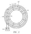
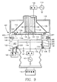
図1を参照すると、プラズマリアクタは、円筒形側壁102、天井104及び床106により囲まれたチャンバ100を有する。ウェハサポート台座108は、床を貫くように延在しており、上昇機構110により、垂直軸に沿って動かすことができる。オーバーヘッドRF電力印加装置は、RF電力をチャンバ100の内側に結合する。図1の実施例において、オーバーヘッドRF電力印加装置は、天井104にある電極112である。電極112は、誘電体リング113により天井104からは電気的に絶縁されている。他の実施形態において、オーバーヘッドRF電極印加装置は、天井を覆う、又は側壁102周囲に配置されたコイルアンテナ(図示せず)である。ウェハサポート台座108は、カソード電極116を囲む上部誘電体部分114と、RF接地に接続された下部導電性基部118とを有していてよい。RFプラズマ電力は、RFインピーダンス整合120を通して、RFジェネレータ119からオーバーヘッド電極112に印加される。RFインピーダンス整合120は、同軸チューニングスタブ(図示せず)であってよい。オーバーヘッド電極112に対するRF供給構造は、同軸であってよく、中空円形中心導体124と、内側導体124と同軸の中空円形外側導体126とを含む。中空中心導体124は、オーバーヘッド電極112及びインピーダンス整合120のRFホット出力に接続されている。外側導体は、RF接地及び天井の接地部分に接続されている。同軸供給構造124及び126は、同軸チューニングスタブと一体化されていてもよい。ウェハの出入りを促すスリットバルブ128は、側壁102を通した浅い開口部として形成されており、図2の平面図に図示する通り、開口部は、側壁102の周囲の約四分の一にわたって延在している。RF電力は、RFインピーダンス整合42を通してRFジェネレータ40からカソード電極116に結合されている。チャンバ100は、チャンバ床のポンピングポート162を通して、真空ポンプ160により排気される。ポンピングアニュラス163は、ウェハサポート台座108と側壁102の間で画定されている。
Referring to FIG. 1, the plasma reactor has a
一実施形態において、オーバーヘッド電極112への全ての設備ラインは、導電性円筒形中空缶130で囲まれており、冷却剤入口ライン132、冷却剤出口ライン134、センサ137(光学発光分光センサ)に結合された光学センサライン136及びプロセスガス供給ライン138を含む。図1に示す実施形態において、オーバーヘッド電極112はまた、複数のガス注入オリフィス112aと内側プロセスガスマニホルド112bを含むガス分配シャワーヘッドでもある。ガス供給ライン138は、内側ガスマニホルド112bに結合されている。オーバーヘッド電極112は、内側冷却剤ジャケット(図示せず)を有することができ、そこでは、冷却剤が入口132から循環して、出口134に戻る。図1に示す実施形態において、全ての設備ライン132、134、136、138は、缶130の内側でもあり、中心同軸導体124内側でもある。
In one embodiment, all equipment lines to the
プラズマ処理中、オーバーヘッド電極/シャワーヘッド112により注入されたプロセスガスは、チャンバ100に結合されたRF電力によりイオン化されて、天井電極112とウェハサポート108の間の処理ゾーンにプラズマを形成する。プラズマからのRF電力は、プラズマから側壁102及び上部電極112まで流されることにより接地に戻る。電流は、側壁102へ、側壁102の表面に沿って、床106周囲に下方に、更に、床106に沿って、ウェハサポート台座108の接地基部118まで半径方向に内側に流れる。図1及び2のリアクタは、概して、対称であって、ウェハサポート台座108周囲で均一又は対称プロセス条件を促進するが、スリットバルブ128やポンピングポート162のような特定のフィーチャーは、側壁102及び半径方向経路に沿って、床の端部からウェハサポート台座の接地基部まで、軸方向下方RF電流リターン経路において、不連続である。これによって、電界分布が不均一となり、このような不均一性は、チャンバの下部ばかりでなく、台座にサポートされるウェハ表面の電界にも影響する。このような不均一性によって、プラズマ処理結果、例えば、ウェハ表面全体のエッチングレート分布に2%の不均一性が導入される。
During plasma processing, the process gas injected by the overhead electrode /
一実施形態において、完全に対称な(非対称の不連続性がない)隆起した導電性グリル200が、ポンピングアニュラス163に提供される。導電性グリル200は、非対称性のない変形の電流路となることにより、RF接地リターン電流路における周方向スキュー源として、ポンピングポート162の不連続性を排除することができる。導電性グリル200は、床からグリルまで間隙201をあけて床106より上にサポートされている。この間隙201は、グリル200を通してガスが流れ、間隙201内でポンピングポート162までスムーズに流れるだけの十分な長さがある。間隙201はまた、RFジェネレータ119の周波数又はRFジェネレータ40の周波数で、グリル200と床106の間の相当の容量結合を防ぐだけの十分な長さがある。
In one embodiment, a fully conductive (no asymmetric discontinuity) raised
導電性グリル200は、導電性側壁102からウェハサポート台座108の接地基部108までの電気路を提供する。図2に示す通り、グリル200は、導電性スポーク210と円形導体215の均一で対称分布パターンを有するため、側壁102から接地台座基部118までの接地リターン路を提供する。これには、周方向スキュー、不均一性、非対称性はない。一実施形態において、全ての接地リターン電流が確実に導電性グリル200を通るようにするために、導電性チャンバ床106を、誘電体リング220により台座基部118から電気的に絶縁する(図1)。リング220の半径方向厚さは、RFジェネレータ119の周波数及びRFジェネレータ40の周波数で容量結合を防ぐのに十分なものとする。スポーク210のあるグリルパターン及びグリル200の導体215は、十分な空間を与えて、チャンバ100からポンプ160までのガスフロー抵抗を最小にする。具体的には、スポーク210及び円形導体215の占める水平面積対グリルの占める合計面積の比率は、グリル200を通るガスフロー抵抗を最小にするのに十分に小さい。一方で、この比率は、RF接地リターン電流のグリルパターンが、ウェハ表面(ワークピースサポート台座108の上部表面)の電界に現れないよう十分に大きい(グリル間隔は十分に小さい)。このため、スポーク210間の間隔は、ウェハサポート台座108の上部表面とグリル200の間の軸方向距離より遥かに狭い。具体的には、例えば、スポーク210間の最大間隔と、台座108の上部とグリル200の間の間隔の比率は、約3倍以上である。
The
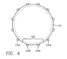
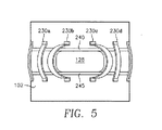
他の実施形態(図3に図示)において、スリットバルブ128の上下にある上下絶縁リング240、245が、側壁102に提供されている。一実施形態において、電気的に絶縁された側壁部分102aをバイパスする電流路が、図4に図示する通り、絶縁部分102aを軸方向に横切るように接続された複数の導電性ストラップ230により提供されている。絶縁リング240、245は、接地リターン路電流分配において周方向スキューの源として、スリットバルブ128により生じる不連続性を排除することができる。導電性ストラップ230により提供される接地リターン路は、スリットバルブの占める側壁102の部分をバイパスする。このバイパス電流路は、チャンバ周囲に対称に分配されている。RF接地リターン電流は、図3に示す通り、スリットバルブ128の占める側壁102の部分102aにおいて、スリットバルブ128の側壁部分102aの夫々上下にある上部絶縁リング240と下部絶縁リング245により、流れが遮断される。誘電体リング240、245の両方がない場合でも、少なくとも1つは存在する。一実施形態において、図4に示す通り、複数の導電性ストラップ230が、側壁102周囲に均一な間隔で配置され、均一な長さ、幅及び厚さを有している。図5に示す通り、ストラップ230は、スリットバルブ128と重なるこれらのストラップ230a、230b、230c、230dは、スリットバルブ128の前を迂回する経路に設けられていて、ウェハの出入りを妨げないようになっている。変形実施形態において、ストラップは、それらの及ぶ分離された側壁部分102aの軸方向長さにより近付く対応する長さを有している。ただし、スリットバルブ128を迂回しなければならないストラップ230a〜230dは、それに対応して長くなっている。一実施形態において、ストラップの長さにおけるこのような差から生じる不均一な電流分布を排除するために、ストラップは全て、均一(又は略均一)なインダクタンスを備えている。この場合、長めのストラップ230a〜230dは、残りの(短めの)ストラップとは異なる幅及び厚さを有しており、幅と厚さの違いは、両方の長さのストラップに同じインダクタンスを与えるように選択されている。2つの異なる長さについて同じインダクタンスを得るための式(1):L=0.0002l[loge(2l/(B+C))+1/2](式中、LはμHでのインダクタンスであり、lはcmでのストラップ長さであり、Bはcmでのストラップ幅であり、Cはcmでのストラップ厚さである)に制限することによりこれは達成される。
In another embodiment (shown in FIG. 3), upper and lower
近接するストラップ230間の間隔dは、接地リターン電流路分布における不連続性を表している。一実施形態において、ストラップ間隔パターンが、ウェハサポート台座108の上部の電界と同様のパターンとならないように、ストラップ間の間隔は、スリットバルブ128の上部からウェハ台座108の上部までの距離より遥かに、例えば、約3倍短い。近接するストラップ230間の間隔は、ストラップ230の幅と周期的な間隔のストラップの数により決まる。ストラップの数は、少なくとも4であり、10以上であってもよい。ストラップの幅は、例えば、円筒形側壁102の周囲の約10分の1であってよい。
The distance d between adjacent straps 230 represents a discontinuity in the ground return current path distribution. In one embodiment, the spacing between the straps is much greater than the distance from the top of the
一実施形態において、絶縁部材400(図3)を側壁102に提供してもよい。絶縁部材は、本実施形態においては、スリットバルブ128を囲んでいる。絶縁部材400は、円筒形側壁の表面にボンドされた誘電体材料であってもよい。一実施形態において、絶縁部材400は、スリットバルブの占める側壁部分102aを横断する短絡を防ぐ。短絡は、例えば、スリットバルブ128が、外部ウェハ搬送チャンバ(図示せず)のポートとインタフェースする時に生じる恐れがある。
In one embodiment, an insulating member 400 (FIG. 3) may be provided on the
一実施形態において、図3に示す通り、高温の導電性グリル200及び周期的な間隔の列をなす導電性ストラップ230は、同じリアクタに含まれている。この組み合わせによって、ポンピングポート162とスリットバルブ128のRF接地リターン電流路不連続性に起因するワークピース電界の周方向スキューが減少又は排除される。オーバーヘッド電極112に供給された設備に起因し得るワークピース電界における他のスキュー又は不均一性は、このような設備供給ラインを全て、円筒形導電性缶130に含めることにより排除される。
In one embodiment, as shown in FIG. 3, the hot
他の実施形態において、図6に示す通り、導電性チャンバ側壁102の上部は、誘電体側壁部分102’に替えられる。天井104全体が、図6に示す通り、誘電体天井104’に替えられる。誘電体側壁部分102’は、天井104’から、プラズマが閉じ込められる傾向となる深さまで、下方に延在している。このフィーチャーによって、側壁102及び床106を通して流れるRF接地リターン電流を防ぐことができる。その結果、スリットバルブ128及びポンピングポート162の不連続性は、電界に影響しない。図6の実施形態において、異なる経路が、導電性環形バッフル260により、プラズマからRF接地リターン電流に提供されている。これは、ワークピースサポート台座の外側導電性ライナ265に接地されている。バッフル260は、プラズマシースと接触するレベルであり、RF接地リターン電流をプラズマから伝導することができる。ライナ265自体は、台座基部118に接地されている。バッフル260と側壁102の間の半径方向間隙270によって、台座上の処理領域からポンピングアニュラス163へガスが流れる。誘電体側壁部分102’は、チャンバの上下部分間での電流の流れを遮断するため、外側同軸導体126は、チャンバの下部、即ち、台座基部118に接地される必要がある。これは、外側同軸導体126と接地基部118の間で、同軸ケーブルの内側導体164を接続することによりなされる。
In another embodiment, as shown in FIG. 6, the top of the
より経済的なアプローチは、図1の導電側壁102を完全に保持することであるが、図6のバッフル260を提供することもある。この組み合わせの一例を、図7及び8に図示する。バッフル260が、台座108と側壁102の間の全距離に少なくとも略及んでいる。図7のバッフル260は、ガス透過性であり、例えば、ガス透過性グリルとして形成される。或いは、バッフル260のガス透過性という特徴は、バッフル260を通して、列をなす軸方向孔を形成することによっても得られる。バッフル260のガス透過性という特徴によって、処理ゾーンからポンピングアニュラス163までガスが流れる。変形実施例において、床106は、絶縁リング220により、台座基部プレート118から電気的に絶縁されていてもよい。リング220は、図7の実施形態における任意のフィーチャーである。これは、RF接地リターン電流が、床106から台座108の接地基部118まで流れるのを防ぐ。一実施形態によれば、導電性側壁は、プラズマからバッフル260まで接地リターン電流を伝導する。このため、バッフル260は、側壁に電気的に結合されている。一実施形態において、これは、導電性側壁102からバッフル260までの低インピーダンス容量結合路により、バッフル260と側壁102の間に機械的な接触を必要とせずに達成される。このフィーチャーによって、金属間の摩擦なしに、ワークピースサポート台座108が上下に動いて、汚染を防ぐことができる。側壁102からバッフル260までの容量結合は、バッフル260の周囲端にサポートされた導電性軸方向フランジ280及び側壁102の内側表面の導電性リッジ287にサポートされた導電性軸方向フランジ285により、図7の実施形態においては実施されている。軸方向フランジ280、285は、十分に小さな空隙290を超えて互いに向き合っており、RFジェネレータ119又はRFジェネレータ40のいずれかの周波数で、非常に低いインピーダンス容量結合を与える。その結果、RF接地リターン電流は、チャンバ100内側のプラズマから側壁102まで、そして、そこからバッフル260まで、バッフルから接地台座ベース118まで流れる。リング絶縁体220は、RF接地リターン電流が、側壁102から接地台座基部118まで流れるのを防ぐ。このように、RF接地リターン電流分布は、ポンピングポート163の存在に影響されないよう、スリットバルブ128を通過して流れず、且つ、スリットバルブ128の存在に影響されないよう、ポンピングポート162を通過して流れない。
A more economical approach is to hold the
バッフル260は、スリットバルブ128の上の位置で、近い間隔のフランジ280、285を介して、側壁102に結合されている。一実施形態において、スリットバルブ128は、バッフル260のレベルの下の側壁102の一部にある。プラズマから側壁102までのRF接地リターン電流は、側壁102に沿って下方に流れるが、フランジ間の空隙290を横断して、バッフル260に引っ張られる(迂回する)ため、通常、バッフル260のレベルの下の側壁102を流れない。一実施形態において、RF接地リターン電流は、スリットバルブ128を含む側壁102の低部環形部分を流れない。その結果、バッフル260の空隙290を横断して、側壁102への結合によって、RF接地リターン電流が、スリットバルブ128に達するのを防ぐ。本実施形態によって、スリットバルブ128が、RF接地リターン電流分布に周方向スキューを形成する傾向を防ぐ又は減じる。
The
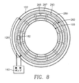
RF接地に周方向スキューを形成する傾向は、図9に図示する通り、スリットバルブ128の上に誘電体リング300を取り付けることによって更に抑制することができる。誘電体リング300の存在によって、側壁102に沿って下方に流れるRF接地リターン電流が、スリットバルブ128により生じる不連続性に達するのを防ぐ。誘電体リング300は、このような不連続性が、RF接地リターン電流分布に影響するのを防ぐ。スリットバルブ不連続性が、電流分布に影響するのを防ぐことによって、電界がワークピースに影響するのを防ぎ、プラズマ処理中のスキュー又は不連続性を防ぐ。
The tendency to create a circumferential skew in the RF ground can be further suppressed by attaching a
上記は本発明の実施形態を対象としているが、本発明の他の更なる実施形態は、その基本的範囲を逸脱することなしに創作することができ、その範囲は特許請求の範囲に基づいて定められる。 While the foregoing is directed to embodiments of the present invention, other and further embodiments of the invention may be made without departing from the basic scope thereof, which scope is based on the claims. Determined.
本発明の上述の実施形態が達成され、詳細に理解できるように、上に簡単に要約した本発明について、添付図面に示した実施形態を参照して、より具体的に説明する。しかしながら、添付図面は本発明の典型的な実施形態を示すに過ぎないため、その範囲を限定するものとは考えられず、本発明は、その他の等しく有効な実施形態も含み得ることに留意すべきである。
理解を促すために、可能な場合は、図面で共通の同一の要素を示すのに、同一の参照番号を用いてある。図面は概略であり、縮尺は合っていない。 To facilitate understanding, identical reference numerals have been used, where possible, to designate identical elements that are common to the figures. The drawings are schematic and not to scale.
Claims (15)
円筒形側壁、天井及び床を有する真空チャンバと、
前記チャンバ中のワークピースサポート台座であって、前記台座と前記側壁の間のポンピングアニュラスが画定されていて、前記床に近接する接地表面を含むワークピースサポート台座と、
RF電力印加装置及び前記天井と前記台座の間に画定されたプロセスゾーンと、
前記床を通るポンピングポートと、
前記台座の前記接地表面と前記床の間の誘電体要素と、
前記ポンピングアニュラス中で、グリルから床まで間隙をあけて前記床より上に配置された環形導電性グリルであって、前記側壁から前記台座の前記接地表面まで電流路を提供し、前記チャンバの対称軸に対して略対称であるグリルとを含むプラズマリアクタ。 A plasma reactor,
A vacuum chamber having cylindrical side walls, a ceiling and a floor;
A workpiece support pedestal in the chamber, the workpiece support pedestal defining a pumping annulus between the pedestal and the side wall and including a grounded surface proximate to the floor;
An RF power application device and a process zone defined between the ceiling and the pedestal;
A pumping port through the floor;
A dielectric element between the ground surface of the pedestal and the floor;
An annular conductive grill disposed in the pumping annulus above the floor with a gap from the grill to the floor, providing a current path from the side wall to the grounded surface of the pedestal, and symmetrical to the chamber A plasma reactor including a grill that is substantially symmetric about an axis.
前記側壁の前記環形部分の軸方向境界に近接する前記円筒形側壁にある少なくとも1つの第1の誘電体リングと、
前記円筒形側壁の前記環形部分をバイパスする軸方向電流流路を提供する列をなす導電性ストラップであって、前記導電性ストラップの夫々が一対の端部を有し、一方の端部は、前記環形部分の上の前記側壁に電気的に接続されており、他方の端部は、前記環形部分の下の前記側壁に電気的に接続されていて、前記ストラップは前記スリットバルブ開口部へのアクセスを妨げないように迂回されている導電性ストラップとを含む請求項1記載のリアクタ。 A slit valve opening through a peripheral portion of the cylindrical side wall, the slit valve being axially restricted within the annular portion of the cylindrical side wall;
At least one first dielectric ring in the cylindrical sidewall proximate to an axial boundary of the annular portion of the sidewall;
Conductive straps in rows providing an axial current flow path that bypasses the annular portion of the cylindrical sidewall, each of the conductive straps having a pair of ends, one end of which is The other end is electrically connected to the side wall above the annular portion and the strap is electrically connected to the slit valve opening. The reactor according to claim 1, further comprising a conductive strap that is bypassed to prevent access.
前記スリットバルブに近接するストラップが、前記スリットバルブの周囲を迂回するだけの十分な長さがあり、残りのストラップはこれより短い長さである請求項5記載のリアクタ。 The strap is configured to provide a uniform inductance to the RF current;
The reactor according to claim 5, wherein the strap adjacent to the slit valve has a sufficient length to bypass the periphery of the slit valve, and the remaining straps have a shorter length.
円筒形側壁、天井及び床を有する真空チャンバと、
前記チャンバ中のワークピースサポート台座であって、前記台座と前記側壁の間のポンピングアニュラスが画定されていて、接地表面を含むワークピースサポート台座と、
RF電力印加装置及び前記天井と前記台座の間に画定されたプロセスゾーンと、
前記床を通るポンピングポート及び前記ポンピングポートに結合された真空ポンプと、
前記円筒形側壁にあるスリットバルブ開口部と、
前記台座から前記側壁に半径方向に延在していて、前記台座を通して接地に電気的に結合された環形バッフルであって、前記プロセスゾーンの軸方向位置と前記スリットバルブの軸方向位置の間の軸方向位置にあるバッフルとを含むプラズマリアクタ。 A plasma reactor for processing a workpiece,
A vacuum chamber having cylindrical side walls, a ceiling and a floor;
A workpiece support pedestal in the chamber, wherein a pumping annulus between the pedestal and the sidewall is defined and includes a ground contact surface;
An RF power application device and a process zone defined between the ceiling and the pedestal;
A pumping port through the floor and a vacuum pump coupled to the pumping port;
A slit valve opening in the cylindrical side wall;
An annular baffle extending radially from the pedestal to the side wall and electrically coupled to ground through the pedestal, between the axial position of the process zone and the axial position of the slit valve A plasma reactor including a baffle in an axial position.
前記バッフルの前記周囲端から軸方向に延在するバッフル軸方向フランジと、
前記側壁の内側表面から半径方向に内側に延在する環形ショルダと、
前記ショルダから軸方向に延在する側壁軸方向フランジとを含み、前記側壁軸方向フランジと前記バッフル軸方向フランジは互いに向き合っていて、RF周波数で容量結合を可能とするだけの十分に小さな間隙により間隔があいている請求項11記載のリアクタ。 The coupling device is
A baffle axial flange extending axially from the peripheral end of the baffle;
An annular shoulder extending radially inward from the inner surface of the sidewall;
A sidewall axial flange extending axially from the shoulder, the sidewall axial flange and the baffle axial flange facing each other and with a gap small enough to allow capacitive coupling at RF frequencies 12. Reactor according to claim 11, which is spaced.
Applications Claiming Priority (1)
| Application Number | Priority Date | Filing Date | Title |
|---|---|---|---|
| US11/828,568 US7988815B2 (en) | 2007-07-26 | 2007-07-26 | Plasma reactor with reduced electrical skew using electrical bypass elements |
Publications (2)
| Publication Number | Publication Date |
|---|---|
| JP2009076870A true JP2009076870A (en) | 2009-04-09 |
| JP2009076870A5 JP2009076870A5 (en) | 2011-09-08 |
Family
ID=40294221
Family Applications (1)
| Application Number | Title | Priority Date | Filing Date |
|---|---|---|---|
| JP2008192135A Withdrawn JP2009076870A (en) | 2007-07-26 | 2008-07-25 | Plasma reactor with reduced electrical skew using electrical bypass element |
Country Status (6)
| Country | Link |
|---|---|
| US (1) | US7988815B2 (en) |
| JP (1) | JP2009076870A (en) |
| KR (1) | KR100984776B1 (en) |
| CN (1) | CN101355004B (en) |
| SG (1) | SG149790A1 (en) |
| TW (1) | TWI358738B (en) |
Cited By (5)
| Publication number | Priority date | Publication date | Assignee | Title |
|---|---|---|---|---|
| US20120024479A1 (en) * | 2010-07-30 | 2012-02-02 | Applied Materials, Inc. | Apparatus for controlling the flow of a gas in a process chamber |
| JP2013503496A (en) * | 2009-08-31 | 2013-01-31 | ラム リサーチ コーポレーション | Radio frequency (RF) ground feedback configuration |
| JP2015517180A (en) * | 2012-03-19 | 2015-06-18 | ラム リサーチ コーポレーションLam Research Corporation | Method and apparatus for selectively modifying an RF current path in a plasma processing system |
| JP2015162266A (en) * | 2014-02-26 | 2015-09-07 | 株式会社日立ハイテクノロジーズ | plasma processing apparatus |
| JP2021184475A (en) * | 2011-10-27 | 2021-12-02 | アプライド マテリアルズ インコーポレイテッドApplied Materials, Incorporated | Process chamber for etching low-k and other dielectric films |
Families Citing this family (22)
| Publication number | Priority date | Publication date | Assignee | Title |
|---|---|---|---|---|
| US8647438B2 (en) | 2007-04-27 | 2014-02-11 | Applied Materials, Inc. | Annular baffle |
| JP5490435B2 (en) * | 2009-03-31 | 2014-05-14 | 東京エレクトロン株式会社 | Gate valve device |
| US8360003B2 (en) * | 2009-07-13 | 2013-01-29 | Applied Materials, Inc. | Plasma reactor with uniform process rate distribution by improved RF ground return path |
| US8578879B2 (en) * | 2009-07-29 | 2013-11-12 | Applied Materials, Inc. | Apparatus for VHF impedance match tuning |
| CN202888133U (en) * | 2009-09-29 | 2013-04-17 | 应用材料公司 | Apparatus for coupling RF (Radio Frequency) power to plasma chamber |
| US8920597B2 (en) | 2010-08-20 | 2014-12-30 | Applied Materials, Inc. | Symmetric VHF source for a plasma reactor |
| WO2012166265A2 (en) | 2011-05-31 | 2012-12-06 | Applied Materials, Inc. | Apparatus and methods for dry etch with edge, side and back protection |
| KR101297264B1 (en) * | 2011-08-31 | 2013-08-16 | (주)젠 | Plasma reactor having dual inductively coupled plasma source |
| US9230779B2 (en) * | 2012-03-19 | 2016-01-05 | Lam Research Corporation | Methods and apparatus for correcting for non-uniformity in a plasma processing system |
| TW201405627A (en) * | 2012-07-20 | 2014-02-01 | Applied Materials Inc | Symmetrical inductively coupled plasma source with coaxial RF feed and coaxial shielding |
| CN103578906B (en) * | 2012-07-31 | 2016-04-27 | 细美事有限公司 | For the treatment of the device of substrate |
| CN103323981A (en) * | 2013-05-24 | 2013-09-25 | 北京京东方光电科技有限公司 | Display panel, manufacturing method thereof and display device |
| US20150075717A1 (en) * | 2013-09-13 | 2015-03-19 | Applied Materials, Inc. | Inductively coupled spatially discrete multi-loop rf-driven plasma source |
| US9412563B2 (en) * | 2013-09-13 | 2016-08-09 | Applied Materials, Inc. | Spatially discrete multi-loop RF-driven plasma source having plural independent zones |
| KR101792941B1 (en) * | 2015-04-30 | 2017-11-02 | 어드밴스드 마이크로 패브리케이션 이큅먼트 인코퍼레이티드, 상하이 | A Chemical Vapor Deposition Apparatus and Its Cleaning Method |
| WO2018121898A1 (en) * | 2016-12-27 | 2018-07-05 | Evatec Ag | Rf capacitive coupled etch reactor |
| JP2019009185A (en) * | 2017-06-21 | 2019-01-17 | 東京エレクトロン株式会社 | Plasma processing apparatus |
| TWI677895B (en) * | 2017-10-30 | 2019-11-21 | 台灣積體電路製造股份有限公司 | Plasma apparatus and monitoring method thereof |
| CN109727837B (en) * | 2017-10-30 | 2021-11-23 | 台湾积体电路制造股份有限公司 | Plasma equipment and plasma equipment monitoring method |
| WO2020106408A1 (en) * | 2018-11-21 | 2020-05-28 | Applied Materials, Inc. | Device and method for tuning plasma distribution using phase control |
| US20210066051A1 (en) * | 2019-08-28 | 2021-03-04 | Applied Materials, Inc. | High conductance lower shield for process chamber |
| USD931241S1 (en) | 2019-08-28 | 2021-09-21 | Applied Materials, Inc. | Lower shield for a substrate processing chamber |
Family Cites Families (10)
| Publication number | Priority date | Publication date | Assignee | Title |
|---|---|---|---|---|
| US5215619A (en) * | 1986-12-19 | 1993-06-01 | Applied Materials, Inc. | Magnetic field-enhanced plasma etch reactor |
| US5210466A (en) * | 1989-10-03 | 1993-05-11 | Applied Materials, Inc. | VHF/UHF reactor system |
| US5891350A (en) * | 1994-12-15 | 1999-04-06 | Applied Materials, Inc. | Adjusting DC bias voltage in plasma chambers |
| US6178919B1 (en) * | 1998-12-28 | 2001-01-30 | Lam Research Corporation | Perforated plasma confinement ring in plasma reactors |
| JP2001077088A (en) * | 1999-09-02 | 2001-03-23 | Tokyo Electron Ltd | Plasma processing device |
| US6296747B1 (en) | 2000-06-22 | 2001-10-02 | Applied Materials, Inc. | Baffled perforated shield in a plasma sputtering reactor |
| JP2002270598A (en) | 2001-03-13 | 2002-09-20 | Tokyo Electron Ltd | Plasma treating apparatus |
| US6652713B2 (en) * | 2001-08-09 | 2003-11-25 | Applied Materials, Inc. | Pedestal with integral shield |
| US8381677B2 (en) * | 2006-12-20 | 2013-02-26 | Applied Materials, Inc. | Prevention of film deposition on PECVD process chamber wall |
| US7972470B2 (en) * | 2007-05-03 | 2011-07-05 | Applied Materials, Inc. | Asymmetric grounding of rectangular susceptor |
-
2007
- 2007-07-26 US US11/828,568 patent/US7988815B2/en not_active Expired - Fee Related
-
2008
- 2008-07-25 JP JP2008192135A patent/JP2009076870A/en not_active Withdrawn
- 2008-07-25 TW TW097128457A patent/TWI358738B/en not_active IP Right Cessation
- 2008-07-25 KR KR1020080073039A patent/KR100984776B1/en not_active IP Right Cessation
- 2008-07-28 SG SG200805595-6A patent/SG149790A1/en unknown
- 2008-07-28 CN CN2008101346270A patent/CN101355004B/en not_active Expired - Fee Related
Cited By (19)
| Publication number | Priority date | Publication date | Assignee | Title |
|---|---|---|---|---|
| KR20210021151A (en) * | 2009-08-31 | 2021-02-24 | 램 리써치 코포레이션 | Radio frequency (rf) ground return arrangements |
| KR102233437B1 (en) | 2009-08-31 | 2021-03-26 | 램 리써치 코포레이션 | Radio frequency (rf) ground return arrangements |
| KR20200117074A (en) * | 2009-08-31 | 2020-10-13 | 램 리써치 코포레이션 | Radio frequency (rf) ground return arrangements |
| KR102201934B1 (en) | 2009-08-31 | 2021-01-11 | 램 리써치 코포레이션 | Radio frequency (rf) ground return arrangements |
| KR102285582B1 (en) | 2009-08-31 | 2021-08-03 | 램 리써치 코포레이션 | Radio frequency (rf) ground return arrangements |
| KR20190101509A (en) * | 2009-08-31 | 2019-08-30 | 램 리써치 코포레이션 | Radio frequency (rf) ground return arrangements |
| KR20190102098A (en) * | 2009-08-31 | 2019-09-02 | 램 리써치 코포레이션 | Radio frequency (rf) ground return arrangements |
| KR102164678B1 (en) | 2009-08-31 | 2020-10-12 | 램 리써치 코포레이션 | Radio frequency (rf) ground return arrangements |
| KR102240849B1 (en) | 2009-08-31 | 2021-04-14 | 램 리써치 코포레이션 | Radio frequency (rf) ground return arrangements |
| KR20210034704A (en) * | 2009-08-31 | 2021-03-30 | 램 리써치 코포레이션 | Radio frequency (rf) ground return arrangements |
| KR102219924B1 (en) | 2009-08-31 | 2021-02-23 | 램 리써치 코포레이션 | Radio frequency (rf) ground return arrangements |
| KR20210006009A (en) * | 2009-08-31 | 2021-01-15 | 램 리써치 코포레이션 | Radio frequency (rf) ground return arrangements |
| JP2013503496A (en) * | 2009-08-31 | 2013-01-31 | ラム リサーチ コーポレーション | Radio frequency (RF) ground feedback configuration |
| US20120024479A1 (en) * | 2010-07-30 | 2012-02-02 | Applied Materials, Inc. | Apparatus for controlling the flow of a gas in a process chamber |
| US9443753B2 (en) * | 2010-07-30 | 2016-09-13 | Applied Materials, Inc. | Apparatus for controlling the flow of a gas in a process chamber |
| JP7250857B2 (en) | 2011-10-27 | 2023-04-03 | アプライド マテリアルズ インコーポレイテッド | Process Chamber for Etching Low-K and Other Dielectric Films |
| JP2021184475A (en) * | 2011-10-27 | 2021-12-02 | アプライド マテリアルズ インコーポレイテッドApplied Materials, Incorporated | Process chamber for etching low-k and other dielectric films |
| JP2015517180A (en) * | 2012-03-19 | 2015-06-18 | ラム リサーチ コーポレーションLam Research Corporation | Method and apparatus for selectively modifying an RF current path in a plasma processing system |
| JP2015162266A (en) * | 2014-02-26 | 2015-09-07 | 株式会社日立ハイテクノロジーズ | plasma processing apparatus |
Also Published As
| Publication number | Publication date |
|---|---|
| KR20090012169A (en) | 2009-02-02 |
| KR100984776B1 (en) | 2010-10-04 |
| CN101355004A (en) | 2009-01-28 |
| US20090025878A1 (en) | 2009-01-29 |
| CN101355004B (en) | 2010-09-08 |
| TW200921742A (en) | 2009-05-16 |
| US7988815B2 (en) | 2011-08-02 |
| TWI358738B (en) | 2012-02-21 |
| SG149790A1 (en) | 2009-02-27 |
Similar Documents
| Publication | Publication Date | Title |
|---|---|---|
| JP2009076870A (en) | Plasma reactor with reduced electrical skew using electrical bypass element | |
| US20090025879A1 (en) | Plasma reactor with reduced electrical skew using a conductive baffle | |
| US9443753B2 (en) | Apparatus for controlling the flow of a gas in a process chamber | |
| US8360003B2 (en) | Plasma reactor with uniform process rate distribution by improved RF ground return path | |
| US20190085467A1 (en) | Plasma Reactor Having Radial Struts for Substrate Support | |
| US7832354B2 (en) | Cathode liner with wafer edge gas injection in a plasma reactor chamber | |
| US7824519B2 (en) | Variable volume plasma processing chamber and associated methods | |
| US20050093460A1 (en) | Helical resonator type plasma processing apparatus | |
| US9870897B2 (en) | Symmetrical plural-coil plasma source with side RF feeds and RF distribution plates | |
| US20040027781A1 (en) | Low loss RF bias electrode for a plasma reactor with enhanced wafer edge RF coupling and highly efficient wafer cooling | |
| US20090159002A1 (en) | Gas distribution plate with annular plenum having a sloped ceiling for uniform distribution | |
| KR20100128285A (en) | Etching chamber having flow equalizer and lower liner | |
| US9449794B2 (en) | Symmetrical inductively coupled plasma source with side RF feeds and spiral coil antenna | |
| TWI452649B (en) | Cathode liner with wafer edge gas injection in a plasma reactor chamber | |
| JPS618927A (en) | Semiconductor wafer plasma etching device | |
| KR20120000231U (en) | - c-shaped confinement ring for a plasma processing chamber | |
| WO2012024116A2 (en) | Symmetric vhf source for a plasma reactor | |
| US20130292057A1 (en) | Capacitively coupled plasma source with rf coupled grounded electrode | |
| KR20150038130A (en) | Symmetrical inductively coupled plasma source with coaxial rf feed and coaxial shielding | |
| US20230170186A1 (en) | Plasma processing apparatus and method for using plasma processing apparatus |
Legal Events
| Date | Code | Title | Description |
|---|---|---|---|
| A521 | Written amendment |
Free format text: JAPANESE INTERMEDIATE CODE: A523 Effective date: 20110722 |
|
| A621 | Written request for application examination |
Free format text: JAPANESE INTERMEDIATE CODE: A621 Effective date: 20110722 |
|
| A761 | Written withdrawal of application |
Free format text: JAPANESE INTERMEDIATE CODE: A761 Effective date: 20120413 |