JP2009059346A - Method and device for connecting with a plurality of multimode processors - Google Patents
Method and device for connecting with a plurality of multimode processors Download PDFInfo
- Publication number
- JP2009059346A JP2009059346A JP2008139702A JP2008139702A JP2009059346A JP 2009059346 A JP2009059346 A JP 2009059346A JP 2008139702 A JP2008139702 A JP 2008139702A JP 2008139702 A JP2008139702 A JP 2008139702A JP 2009059346 A JP2009059346 A JP 2009059346A
- Authority
- JP
- Japan
- Prior art keywords
- processor
- mode
- processors
- array
- routing
- Prior art date
- Legal status (The legal status is an assumption and is not a legal conclusion. Google has not performed a legal analysis and makes no representation as to the accuracy of the status listed.)
- Pending
Links
- 238000000034 method Methods 0.000 title claims abstract description 35
- 238000012545 processing Methods 0.000 claims abstract description 57
- 230000008569 process Effects 0.000 claims abstract description 9
- 230000008859 change Effects 0.000 claims description 2
- 238000004891 communication Methods 0.000 description 10
- 238000003491 array Methods 0.000 description 6
- 230000006872 improvement Effects 0.000 description 5
- 230000010365 information processing Effects 0.000 description 5
- 238000004364 calculation method Methods 0.000 description 4
- 238000010586 diagram Methods 0.000 description 4
- 230000008901 benefit Effects 0.000 description 3
- 238000005516 engineering process Methods 0.000 description 3
- 230000002093 peripheral effect Effects 0.000 description 3
- 230000007704 transition Effects 0.000 description 3
- 230000003044 adaptive effect Effects 0.000 description 2
- 230000005540 biological transmission Effects 0.000 description 2
- 230000006870 function Effects 0.000 description 2
- 230000020169 heat generation Effects 0.000 description 2
- 238000012986 modification Methods 0.000 description 2
- 230000004048 modification Effects 0.000 description 2
- 239000004065 semiconductor Substances 0.000 description 2
- 230000003466 anti-cipated effect Effects 0.000 description 1
- 238000006243 chemical reaction Methods 0.000 description 1
- 238000004883 computer application Methods 0.000 description 1
- 239000004020 conductor Substances 0.000 description 1
- 230000001419 dependent effect Effects 0.000 description 1
- 238000005457 optimization Methods 0.000 description 1
- 230000004044 response Effects 0.000 description 1
Images


Classifications
-
- G—PHYSICS
- G06—COMPUTING; CALCULATING OR COUNTING
- G06F—ELECTRIC DIGITAL DATA PROCESSING
- G06F15/00—Digital computers in general; Data processing equipment in general
- G06F15/16—Combinations of two or more digital computers each having at least an arithmetic unit, a program unit and a register, e.g. for a simultaneous processing of several programs
- G06F15/163—Interprocessor communication
- G06F15/173—Interprocessor communication using an interconnection network, e.g. matrix, shuffle, pyramid, star, snowflake
- G06F15/17356—Indirect interconnection networks
- G06F15/17368—Indirect interconnection networks non hierarchical topologies
- G06F15/17381—Two dimensional, e.g. mesh, torus
-
- G—PHYSICS
- G06—COMPUTING; CALCULATING OR COUNTING
- G06F—ELECTRIC DIGITAL DATA PROCESSING
- G06F13/00—Interconnection of, or transfer of information or other signals between, memories, input/output devices or central processing units
- G06F13/10—Program control for peripheral devices
- G06F13/12—Program control for peripheral devices using hardware independent of the central processor, e.g. channel or peripheral processor
-
- G—PHYSICS
- G06—COMPUTING; CALCULATING OR COUNTING
- G06F—ELECTRIC DIGITAL DATA PROCESSING
- G06F15/00—Digital computers in general; Data processing equipment in general
- G06F15/16—Combinations of two or more digital computers each having at least an arithmetic unit, a program unit and a register, e.g. for a simultaneous processing of several programs
- G06F15/163—Interprocessor communication
- G06F15/173—Interprocessor communication using an interconnection network, e.g. matrix, shuffle, pyramid, star, snowflake
- G06F15/17337—Direct connection machines, e.g. completely connected computers, point to point communication networks
-
- G—PHYSICS
- G06—COMPUTING; CALCULATING OR COUNTING
- G06F—ELECTRIC DIGITAL DATA PROCESSING
- G06F15/00—Digital computers in general; Data processing equipment in general
- G06F15/76—Architectures of general purpose stored program computers
- G06F15/80—Architectures of general purpose stored program computers comprising an array of processing units with common control, e.g. single instruction multiple data processors
- G06F15/8007—Architectures of general purpose stored program computers comprising an array of processing units with common control, e.g. single instruction multiple data processors single instruction multiple data [SIMD] multiprocessors
-
- G—PHYSICS
- G06—COMPUTING; CALCULATING OR COUNTING
- G06F—ELECTRIC DIGITAL DATA PROCESSING
- G06F9/00—Arrangements for program control, e.g. control units
- G06F9/06—Arrangements for program control, e.g. control units using stored programs, i.e. using an internal store of processing equipment to receive or retain programs
- G06F9/30—Arrangements for executing machine instructions, e.g. instruction decode
- G06F9/38—Concurrent instruction execution, e.g. pipeline or look ahead
Landscapes
- Engineering & Computer Science (AREA)
- Theoretical Computer Science (AREA)
- Computer Hardware Design (AREA)
- Physics & Mathematics (AREA)
- General Engineering & Computer Science (AREA)
- General Physics & Mathematics (AREA)
- Software Systems (AREA)
- Mathematical Physics (AREA)
- Computing Systems (AREA)
- Multi Processors (AREA)
Abstract
Description
本発明は、コンピュータおよびコンピュータプロセッサの分野に関し、より詳細には、コンピュータを互いに接続するための方法および装置に関する。 The present invention relates to the field of computers and computer processors, and more particularly to methods and apparatus for connecting computers together.
複数のプロセッサまたはコンピュータを使用して演算を高速化することは、コンピュータの多数の情報処理アプリケーションにおいて効果的である。タスクを分配し、複数の処理とコンピュータ演算を同時に並行して行うことは、多数のシステムと構造を用いてそれらを行う公知の技術である。一例として、シストリックアレイの処理では、大規模の情報ストリームは、列による逐次計算を行い、その結果を次の列に渡すプロセッサの行の中で分配される。他の例は、スーパーコンピュータの分野で見られ、そこでは複数のプロセッサを相互接続することができ、いくつかの異なる方法でそれらに割り当てられたタスク、プロセッサと新しいデータとの間の中間結果の通信、およびそれらの命令は、クロスバースイッチ、ルータ付きまたはルータ無しのバス相互接続のネットワーク、大型コンピュータに使用されるMPICH等のメッセージを受け渡すプロトコルを有するプロセッサ間の直接相互接続を介して提供できる。 Speeding up operations using multiple processors or computers is effective in many information processing applications on computers. Distributing tasks and performing multiple processes and computer operations simultaneously in parallel is a well-known technique for performing them using multiple systems and structures. As an example, in systolic array processing, a large information stream is distributed among the rows of processors that perform sequential computation by column and pass the result to the next column. Another example is found in the field of supercomputers where multiple processors can be interconnected and tasks assigned to them in several different ways, intermediate results between the processor and new data Communication, and instructions are provided via cross-bar switches, network of bus interconnects with or without routers, direct interconnects between processors with protocols such as MPICH used for large computers it can.
半導体技術における継続的な進歩のおかげで、情報量と処理速度が向上した回路を、マイクロチップの領域に設置できる。家庭用および業務用電気製品にある埋め込み式システムとして新しい機能および最適化を提供する単一チップのマイクロプロセッサアレイおよびマイクロコアプロセッサは、非常に高速で計算を行うことにより、大きな経済利益を生む改善例である。従って、複数のプロセッサおよびそれらの相互接続のさらなる改良は、特に単一マイクロチップにおいてきわめて望ましい。 Thanks to continuous advances in semiconductor technology, circuits with improved information content and processing speed can be installed in the microchip area. Single-chip microprocessor arrays and microcore processors that offer new capabilities and optimizations as embedded systems in home and commercial appliances, improve at a huge economic benefit by performing calculations at very high speeds It is an example. Thus, further improvements in multiple processors and their interconnections are highly desirable, especially in a single microchip.
本発明の一態様では、複数のプロセッサを備えたコンピュータアレイを提供する。各プロセッサは、各リンクが2つのプロセッサのみに接続されているリンクによって、少なくとも2つの隣接プロセッサに接続され、前記複数のプロセッサは、前記リンクの命令を受信すると待機モードとアクティブモードとの間で切り替えが可能である。 In one aspect of the present invention, a computer array comprising a plurality of processors is provided. Each processor is connected to at least two neighboring processors by a link where each link is connected to only two processors, and the plurality of processors are in between a standby mode and an active mode upon receiving the link instructions. Switching is possible.
一実施形態では、リンクは、少なくとも1つのデータ回線および好ましくは複数のデータ回線を備える。一実施形態では、そのリンクは、少なくとも1つの制御回線および好ましくは複数の制御回線も備える。それらの制御回線は、一方向性とすることができる。 In one embodiment, the link comprises at least one data line and preferably a plurality of data lines. In one embodiment, the link also comprises at least one control line and preferably a plurality of control lines. Those control lines can be unidirectional.
コンピュータアレイの一実施形態では、前記アレイの端部の複数のプロセッサは、3つの隣接プロセッサに接続している3つのリンクを有し、前記アレイの各角の前記4つのプロセッサは、前記アレイの端部の前記2つのプロセッサに接続している2つの付随リンクを有し、前記アレイの端部でも角でもないプロセッサに接続された前記端部のプロセッサの前記リンクが1つのハイブリッドプロセッサに接続されている、4つのプロセッサにつながる4つリンクによって接続された複数のハイブリッドプロセッサを有する。前記アレイの角の複数のプロセッサは、メモリ、入力装置、ディスプレイ装置、および処理装置のグループから選択された外部装置に接続するように適用できる。前記アレイの端部の複数のプロセッサは、メモリ、入力装置、ディスプレイ装置、および処理装置のグループから選択された外部装置に接続するように適用できる。 In one embodiment of the computer array, the plurality of processors at the end of the array have three links connected to three adjacent processors, and the four processors at each corner of the array The link of the end processor connected to a processor that is neither an end nor a corner of the array is connected to a single hybrid processor having two associated links connected to the two processors at the end. A plurality of hybrid processors connected by four links leading to the four processors. The plurality of processors in the corner of the array can be adapted to connect to an external device selected from the group of memory, input device, display device, and processing device. The plurality of processors at the end of the array can be adapted to connect to an external device selected from the group of memory, input device, display device, and processing device.
一実施形態では、前記ハイブリッドプロセッサは、それらに接続されたリンクから命令を受信すると経路指定モード、処理モード、および待機モードの間で切り替えができる。その実施形態では、前記各リンクは、データ回線および制御回線を備えることができ、前記命令は、前記データ回線上を通るデジタルワードである。前記デジタルワードを経路指定ワードにして、前記プロセッサに経路指定モードに切り替えさせることができる。前記デジタルワードを処理ワードにして、前記プロセッサに処理モードに切り替えさせることができる。 In one embodiment, the hybrid processors can switch between a routing mode, a processing mode, and a standby mode upon receiving an instruction from a link connected to them. In that embodiment, each link may comprise a data line and a control line, and the command is a digital word passing over the data line. The digital word can be a routing word to cause the processor to switch to a routing mode. The digital word can be used as a processing word to cause the processor to switch to a processing mode.
本発明のもう一つの態様では、前記プロセッサを2つの直接隣接したプロセッサに接続する少なくとも2つのリンクに接続するように適用された中央処理装置と、前記リンクのいずれかの命令により、前記中央処理装置を待機モードからアクティブモードにシフトさせる前記中央処理装置に接続されたメモリ装置を備えたコンピュータアレイで使用するプロセッサを提供する。 In another aspect of the present invention, a central processing unit adapted to connect the processor to at least two links connecting two directly adjacent processors, and the central processing unit according to any instruction of the link A processor for use in a computer array having a memory device connected to the central processing unit for shifting the device from a standby mode to an active mode is provided.
前記中央処理装置を、4つの直接隣接したプロセッサに接続する全部で4つのリンクに対して、前記プロセッサを2つの付加的な直接隣接したプロセッサに接続する少なくとも2つの付加的なリンクに接続するようにさらに適用できる。それらのメモリ装置は、ROMメモリおよびRAMメモリを備えることができる。一実施形態では、前記各リンクは、データ回線および制御回線をさらに備え、前記命令は、前記データ回線上を通るデジタルワードである。それらの制御回線を、一方向性にできる。 For a total of four links connecting the central processing unit to four directly adjacent processors, connecting the processor to at least two additional links connecting two additional directly adjacent processors. Further applicable to. These memory devices can comprise ROM memory and RAM memory. In one embodiment, each link further comprises a data line and a control line, and the command is a digital word passing over the data line. These control lines can be unidirectional.
コンピュータアレイで使用するプロセッサの一実施形態では、前記中央処理装置は、3つのモードである電力を節約するための待機モードである第一モードと、経路指定タスクを行うための経路指定モードである第二モードと、処理タスクを行うための処理モードである第三モードを有し、前記リンクのうちの1つから命令を受信すると前記処理装置のモードの切り替えが起きる。 In one embodiment of a processor for use in a computer array, the central processing unit is in three modes: a first mode that is a standby mode for conserving power and a routing mode for performing routing tasks. There is a second mode and a third mode, which is a processing mode for performing a processing task, and when a command is received from one of the links, the mode of the processing device is switched.
前記中央処理装置は、経路指定接続ワードを受信すると待機モードから経路指定モードにシフトし、経路指定タスクが終了するまで経路指定モードの状態のままであり、その後で待機モードに戻る。 When the central processing unit receives the routing connection word, it shifts from the standby mode to the routing mode, remains in the routing mode until the routing task ends, and then returns to the standby mode.
前記中央処理装置は、処理コマンドワードを受信すると待機モードから処理モードにシフトし、処理のタスクが終了するまで処理モードの状態のままであり、その後で待機モードに戻る。 When receiving the processing command word, the central processing unit shifts from the standby mode to the processing mode, remains in the processing mode until the processing task is completed, and then returns to the standby mode.
本発明のさらなる態様では、前記アレイの一部のプロセッサを、少なくとも待機モードとタスクを実行する別のモードを有するマルチモードプロセッサとして指定するステップと、コマンドワードを受信すると前記指定されたプロセッサが前記他のモードに切り替わるステップと、前記コマンドワードを受信するとタスクを実行するステップと、前記タスクが終了すると再び待機モードに切り替わるステップを備えたマルチプロセッサアレイを操作する方法を提供する。それらの方法は、経路指定ワードまたは処理コマンドワードを受信すると前記指定されたプロセッサが経路指定モードまたは処理モードに切り替わるステップと、前記受信のあとで経路指定タスクまたは処理タスクを実行するステップと、前記経路指定タスクまたは処理タスクが終了すると待機モードに戻るステップをさらに備えることができる。 In a further aspect of the invention, designating a processor of a portion of the array as a multi-mode processor having at least a standby mode and another mode for performing a task, and the designated processor upon receiving a command word, A method of operating a multiprocessor array comprising the steps of switching to another mode, executing a task upon receipt of the command word, and switching back to standby mode when the task is completed. The methods include the step of switching the designated processor to a routing mode or processing mode upon receipt of a routing word or processing command word, executing a routing task or processing task after the receiving, and The method may further comprise returning to the standby mode when the routing task or the processing task is completed.
本発明のマルチプロセッサアレイおよび方法は、マルチプロセッサアレイが、特にオペレーティングシステムのプログラム命令の実質的な大部分を占めるローカルメモリを有する複数のフォンノイマン型計算機として動作するように適用されている大型のアプリケーションで使用することができる。 The multiprocessor array and method of the present invention is a large-scale application where the multiprocessor array is adapted to operate as a plurality of von Neumann computers with local memory that occupies substantially the majority of operating system program instructions. Can be used in application.
本発明は、各コンピュータアレイがプロセッサの領域を含み、各プロセッサが別個のメモリを含むいくつかのコンピュータアレイを含むことができる。それらのプロセッサは、リンクを用いて直接隣接するプロセッサに接続される。本発明の実施形態では、異なるタイプのデータ回線および制御回線を含むいくつかのリンクの構成が使用される。PCW(Process Command Words)およびRCW(Routing Connection Words)が、プロセッサ間のそれらのリンクを通って、アレイの中の少なくとも1または複数のプロセッサのモードを変更する方法を提供する。 The present invention can include several computer arrays in which each computer array includes an area of a processor and each processor includes a separate memory. These processors are connected to the directly adjacent processors using links. In an embodiment of the present invention, several link configurations including different types of data lines and control lines are used. PCW (Process Command Words) and RCW (Routing Connection Words) provide a way to change the mode of at least one or more processors in the array through their links between the processors.
これらの方法の利用により、電力消費を最小限にすると同時に演算資源のより効果的な配分を確実にする。これらの方法により、演算資源の効果的な配分と外部メモリ、周辺機器等のアレイの外部からの資源に接続することがさらに可能である。 Use of these methods ensures a more effective allocation of computing resources while minimizing power consumption. By these methods, it is further possible to effectively allocate computing resources and connect to external resources such as external memory and peripheral devices.
本発明を適用して単一マイクロチップ上で複数のコンピュータの組み合わせを用いて直接実行することができる。ここでの演算効率は、演算スピードを増加させる要望のためだけでなく、結果として大幅に効率が上がる節電と発熱を削減するためにも重要である。 The present invention can be applied to directly execute a combination of a plurality of computers on a single microchip. The calculation efficiency here is important not only for the demand for increasing the calculation speed, but also for reducing the power saving and the heat generation that result in a significant increase in efficiency.
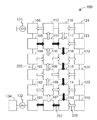
図1に、一つのマイクロチップに載せることができる4×6のアレイに配置された24個のプロセッサ101−124を備えるマルチプロセッサアレイ100を示す。プロセッサの他の数および他の配置が、発明の範囲内で選択的に可能であることは、当業者には明らかである。具体例では、各プロセッサは、18ビットのワードサイズ、512ワードのRAMおよび512ワードのROMを含むローカルメモリを有することも可能である。これらのパラメータは、発明に制限を与えるものでなく、演算は、その装置の作動が十分可能なメモリの量で動作できる。具体的な目的のために記載されたこの特殊なプロセッサは、32−命令RISC第4版のコンピュータ言語のみを機械語として用いる。本発明では、適応するプロセッサを用いて2進数形式にコンパイル化されたC言語を含む任意の適応する機械語を用いて実施できることがわかる。図1に示すように、101、102、103−124の各プロセッサは、リンク200を相互接続することによってそれぞれが最も近接するプロセッサに接続される。アレイの中央のプロセッサ108−111および114−117は、4つの相互接続リンク200を有する。
FIG. 1 shows a
角のプロセッサ101、106、119、および124は、2つのみの相互接続リンク200を有する。この具体例では、角のプロセッサ101および106は、入力/出力ポート131と132のそれぞれに接続された西側のポートを有する。アレイに接続された外部入力/出力(i/o)接続131および132は、外部装置133および134と通信を行う汎用のためのものである。外部入力および外部出力は、データおよびある命令のためのものである。以下でさらに説明するように、これらの命令およびデータは、アレイのプロセッサによって共有され、一般的にプロセッサの個別の制御によって動作する。101および106以外のアレイのプロセッサは、中間のプロセッサおよびそれらの相互接続リンク200を介して情報を経路指定することにより通信を行う。外部装置133および134ならびにアレイの他のプロセッサ間の情報の配信は、プロセッサ101および106の主要なタスクである。従ってプロセッサ101および106は、サーバプロセッサと見なされる。ポート131および132は、センサ、外部メモリ装置、ディスプレイ装置、入力装置、または典型的にプロセッサに接続される任意の装置から選択できる外部装置133および134に接続できる。このような発明の実施形態では、前記入力/出力接続は、プロセッサ101から外部メモリ装置133までのポート220へつなぐ制御回線、データ回線、およびアドレス回線と、公知の標準に従い実装される。また、当該技術分野で周知のように、プロセッサ106を外部のSPI(serial peripheral interface)装置134に接続するポート132を介したイネーブル回線、クロック回線、データイン回線、およびデータアウト回線によって実施できる。代わりの実施形態において、サーバプロセッサと同数で提供される外部入力/出力(i/o)装置および接続が1または2以上あり得ることは、当業者には明らかである。外部装置133、134は、マルチプロセッサアレイとして同じマイクロチップ上に配置でき、それらはメモリ装置とデータ通信のインタフェース装置の任意の組み合わせを選択的に備えることができる。さらなる実施形態では、1以上のマルチプロセッサアレイ、および用途に応じて必要とする任意の付加的な回路は、1つのマイクロチップ上に配置できる。
The
端部の102−105、107、112、113、118、および120−123の各プロセッサは、3つの接続リンク200を有する。マルチプロセッサアレイ100は、主にアレイの周辺にあるこれらのプロセッサを用いて、特に現行のアプリケーションの情報処理要求が低い場合には、プロセッサ102−105および119−124を用いて計算を行うために適用される。プロセッサ102−105および119−124を、クライアントプロセッサと呼ぶこともできる。他の用途では、プロセッサ102−105および119−124は、適応するポート(図示せず)を用いてアナログ・デジタル変換機、高速フーリエ変換、およびデジタル・アナログ変換を含むアクティブポートとして機能することによって入力/出力プロセッサとしても作動できる。
Each of the end processors 102-105, 107, 112, 113, 118, and 120-123 has three connecting
アレイの内側の2つのカラムであるプロセッサ107−118は、本明細書ではRモードと呼ばれる、任意の時点でアレイの別のプロセッサへの経路指定情報であるか、本明細書ではPモードと呼ばれる、計算および情報処理タスクを行うか、または本明細書ではIモードと呼ばれる、待機状態であるハイブリッドプロセッサに適用される。Iモードは、演算電力を低減させるデフォルト条件であり、ハイブリッドプロセッサは、演算または他の2つのモードにおける一連の演算の終了後、自動的にIモードに戻る。それは節電機能であり、特にバッテリ電源式システムの用途において有効である。情報処理要求が低い状態では、ハイブリッドプロセッサ107−118は、一般的にIモードであり、入力および出力動作がクライアントプロセッサ102−105および119−124によって要求された場合、適宜Rモードに切り替わる。ハイブリッドプロセッサ107−118は、相互接続リンクの任意の1つである複数のデータ回線200上でRCW(Routing Connection Word)のアサーションに応じてRモードに切り替わるように適用される。周知の技術を使用して、各クライアントプロセッサおよびサーバプロセッサの往復の経路指定パスは、アレイの作成中または後のアレイの再構成の間のコンパイル時間に、メモリに格納されたファームウェアで、あらかじめ決められている。
The two columns inside the array, processor 107-118, are referred to herein as R mode, routing information to another processor in the array at any point in time, or referred to herein as P mode. It applies to a hybrid processor that performs computation and information processing tasks or is in a standby state, referred to herein as I-mode. The I mode is a default condition for reducing the computation power, and the hybrid processor automatically returns to the I mode after the computation or a series of computations in the other two modes. It is a power saving function and is particularly useful in battery powered system applications. In a state where the information processing request is low, the hybrid processor 107-118 is generally in the I mode, and when the input and output operations are requested by the client processors 102-105 and 119-124, the hybrid processor 107-118 is appropriately switched to the R mode. The hybrid processors 107-118 are applied so as to switch to the R mode in response to an RCW (Routing Connection Word) assertion on a plurality of
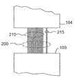
図2に、プロセッサ103と104との間のより詳細なリンク200を示し、各リンク200は、複数の相互接続回線であり、当該技術分野において時々ワンドロップ・バスネットと呼ばれる。この例で、各リンク200は、18本のデータ回線210および2本の制御回線215を複数含み、双方向および非同期的に動作するように適用される。ハイブリッドプロセッサ107−118は、それぞれの制御回線215で対応する信号に従属した他のプロセッサを有する相互接続リンクの任意の1つである複数のデータ回線210上でRCW(Routing Connection Word)のアサーションに応じてRモードに切り替わるように適用される。第2の実施形態に従って、複数の200は、同期的および一方向に動作するように適用された36本のデータ回線および4本のデータ回線を備えることができ、それらの回線の半分は一方向であり、もう半分は逆方向である。発明の他の実施形態ではさらに、ワードサイズ、メモリサイズ、コンピュータ言語、および相互接続回線の数を含む様々な共通のプロセッサの特性を使用できる。本明細書の回線は、マルチレイヤマイクロチップと同じおよび異なる階層に配置することができるバイアスと電気的な直列を交互に用いた1または複数の導電性材料片を備えるマイクロチップの表面にある電気的に導電性の線であると考えられる。前記プロセッサおよびリンクを、半導体集積回路以外の技術において、例えば集積光学または、分子および科学の情報処理装置を、当該技術に従って作成された適応する改良を用いて選択的に実施できることが本発明に従ってさらに予想される。
FIG. 2 shows more
図3に、アレイ100のあらかじめ決められた経路の1セットを、クライアントプロセッサ102―105および119−124からサーバプロセッサ101および106までの書き込み命令の方向を示した白抜き矢印250および黒矢印252によって示す。読み取り命令の場合、経路指定パスは、最初はコマンドを渡すための所定の方向になり、次にその情報を戻すために逆方向になる。特殊な例として、プロセッサ105による書き込み操作に対する、入力/出力接続220およびサーバ101上のメモリ装置320までの経路指定パスは、情報伝送の間Rモードで動作するハイブリッドプロセッサ111、117、116、115、114、113および107を介して進むようにあらかじめ決めることができ、この経路は、黒矢印252によって示される。
In FIG. 3, a set of predetermined paths of the
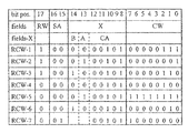
図4に、各行が、最も左の列で標示または指定されたように、RCWの代表を示すために用いられたRCWのフォーマットを示す。プロセッサワードのビット位置は、図4の行の最上位にあり、ビットで表されたRCWの情報フィールドは、2番目の行に記されている。各ビット位置は、周知の技術として図2を参照して上記に説明された第一の実施形態で、特定の双方向および非同期的に動作する複数の210のデータ回線に対応し、第2の実施形態で、特定のペアである同期的および一方向に動作する複数の210のデータ回線に対応する。特に最下位の8つのビット(ビット位置0から7)は、経路指定される情報のCW(word count)を含む。最上位のビット(ビット17)は、情報伝送の方向を特定する読み取りまたは書き込み指示子RWであり、例えば外部装置への読み取り動作に対して1および書き込み動作に対して0である。ビット15および16は、SA(server address)を保持し、本実施例ではサーバプロセッサ101または106を識別する00または01にできる。ビット8から14は、アプリケーション専用の情報Xを含むことができ、図4の3番目の行および続く行を参照して以下でより詳細に説明される。RCWを受信するハイブリッドプロセッサ111、117、116、115、114、113および107の中の1つは、相互接続リンクの1つにアサートされたこのRCWを有することにより、RCWのコピーを格納し、SAによって識別されたサーバプロセッサ101および106に対するあらかじめ決められたパスに沿って、それを変更されていない次のプロセッサに渡す。書き込みの場合、経路指定される情報のCWワードは、直ちにRCWの後に続き、読み取りの場合、RCWがサーバプロセッサ101および106ならびに関連した外部装置131および133に到達した後、情報のCWワードは、あらかじめ決められた同じパスに沿って反対方向で戻ることができる。ハイブリッドプロセッサ111、117、116、115、114、113および107は、CWのよって特定された数のワードが経路指定された後、自動的にIモードに戻るように適用される。
FIG. 4 shows the format of the RCW that was used to show the representative of the RCW as each row was labeled or designated in the leftmost column. The bit position of the processor word is at the top of the row in FIG. 4, and the RCW information field expressed in bits is written in the second row. Each bit position corresponds to a particular plurality of 210 data lines operating in a bi-directional and asynchronous manner in the first embodiment described above with reference to FIG. In an embodiment, a particular pair of 210 data lines operating synchronously and unidirectionally is supported. In particular, the lowest 8 bits (
フィールドXは、図4の3番目の行に示すような下位フィールドに分割でき、ビット8−12をクライアントプロセッサのアドレスCAに指定し、ビット13および14を切り替え命令AおよびBに指定して、プライベートブロック(ビット値1)かまたはメモリ(ビット値0)の共用領域を特定する。
Field X can be divided into lower fields as shown in the third row of FIG. 4, with bits 8-12 designated as client processor address CA,
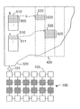
図5は、マイクロプロセッサアレイ100の外部RAM装置133の図である。メモリのいくつかの区分を特定できる。RCWのアプリケーション専用の情報フィールドXを使用してアレイのクライアントプロセッサによって共用される外部RAM装置133と通信できる。外部RAMは、各クライアントプロセッサに対して2つのプライベートの情報ブロックを有することができ、それらはブロックA、ブロックBと呼ばれ、一般に図中点線の列によって示されるメモリの共用領域420である。ブロックAを読み取り制御のために使用して、情報が読み取られるRAMの一般領域にあるアドレスを特定でき、ブロックBを書き込み制御のために使用して、情報が書き込まれる前記一般領域にあるアドレスを特定できる。特にプライベートブロックは、各クライアントプロセッサのRAMの一般領域への次のアクセスのための開始アドレスを保持し、前記ブロックを、サーバプロセッサによって各アクセスで自動的に増やすことができる。
FIG. 5 is a diagram of the external RAM device 133 of the
クライアントプロセッサによって行うことができるいくつかの異なる外部RAM動作に対する標示されたRCW−1からRCW−6までのRCWの例は、各特定のRCWに対して図5のメモリブロックを参照して図4の他の行に示される。上記で説明したようにRWビット17は、読み取り動作に対して1および書き込み動作に対して0とする。本目的のために、外部RAM装置133に接続するサーバプロセッサ101のアドレスSAは、00とすることができ、クライアントプロセッサは、CAアドレス00101を用いてプロセッサ105とすることができる。発明方法は、特殊な実施形態およびプロセッサを参照して本明細書で説明されるが、説明されたRCWの発明の使用が、アドレスおよび経路指定パスに適応する改良を用いて他のプロセッサおよび実施形態にも等しく効果的であることは当業者には明らかである。
An example RCW-1 through RCW-6 RCW example for several different external RAM operations that can be performed by the client processor is shown in FIG. 4 with reference to the memory block of FIG. 5 for each particular RCW. Shown on other lines. As explained above, the
経路指定接続ワードRCW−1は、読み取り動作を指定するRWフィールドに1を有し、切り替えフィールドAおよびBの両方に0、CWフィールド(CW=7)に00000111を有し、クライアントプロセッサ105に対するプライベートの読み取り制御ブロックAの最上位のメモリ配置510で特定されるRAMの共用領域にあるアドレスから読み取られる情報の7ワードを呼び出す。それらのアドレスは例えば、図中点線の矢印で示されるようにメモリ配置520を特定する。従ってRCW−1は、クライアントプロセッサ105(に転送されること)によって読み取られる外部RAMの共用領域にある情報の7ワードのブロック525の内容を呼び出す。この動作の後、ブロックAの最上位を配置511に増分させ、RAMの共用領域からのクライアントプロセッサ105による次の読み取り動作は、511で特定されたアドレスによって起きる。
The routing connection word RCW-1 has 1 in the RW field designating the read operation, 0 in both switching fields A and B, 00000111 in the CW field (CW = 7), and is private to the
図4のRCW−2は、RWフィールドに1、ブロックの切り替えフィールドAに1、およびCW=1を有し、RCW−2はRCW−1の後に続くと仮定して、ブロックAの最上位、つまり配置511から読み取られる情報の1ワードを呼び出す。これにより、クライアントプロセッサ105に外部RAMの共用領域から次の読み取りのアドレスを伝えることができる。
RCW-2 in FIG. 4 has 1 in the RW field, 1 in the block switching field A, and CW = 1, and RCW-2 follows RCW-1, the top of block A, That is, one word of information read from the
次の行のRCW−3もRWフィールドに1、ブロックの切り替えフィールドBに1、およびCW=6を有し、配置610から開始するブロックBの最上位から読み取られる情報の6ワードのブロック655を呼び出す。これにより、クライアントプロセッサに共用領域に対する次の6つの書き込み動作のアドレスを伝えることができる。
The next row RCW-3 also has 1 in the RW field, 1 in the block switching field B, and CW = 6, and a 6-word block 655 of information read from the top of block B starting from
次の行のRCW−4は、RWフィールドに0、切り替えフィールドAおよびBの両方に0、およびCW=4を有し、書き込まれる(プロセッサ105から転送される)情報の4ワードのブロックの情報を、現行の書き込み制御ブロックBの最上位に位置する配置610で特定されるアドレスから開始する共用のメモリ領域に導く。それらのアドレスは、図5に点線の矢印で示すようにメモリ配置620を特定する。従って620から開始する4つのメモリ配置のブロック625は、クライアントプロセッサ105からの新しい情報で埋められる。
RCW-4 in the next row has 0 in the RW field, 0 in both switching fields A and B, and CW = 4, and the information of the 4-word block of information to be written (transferred from processor 105) To the shared memory area starting from the address specified by the
RCW−5もRWフィールドに0、切り替えフィールドAに1、およびCW=255を有し、現行の最上位の配置から開始するプロセッサ105に対する読み取り制御ブロックAに書き込まれる情報の255ワードのブロックを呼び出す。このため、共用領域からの105によって次の255の読み取り動作のアドレスをアップデートするのに効果がある。
RCW-5 also has 0 in the RW field, 1 in the switch field A, and CW = 255, and calls a 255 word block of information to be written to the read control block A for the
RCW−6もRWフィールドに0、切り替えフィールドBに1、およびCW=2を有し、例えばRCW−3によって読み取られる情報に基づいて、共用領域への次の2つの書き込み動作の手順を逆にするために、アップデートされる書き込み制御ブロックBの最上位の2つの配置を呼び出す。 RCW-6 also has 0 in the RW field, 1 in the switching field B, and CW = 2. For example, based on the information read by the RCW-3, the procedure of the next two write operations to the shared area is reversed. In order to do this, the top two arrangements of the write control block B to be updated are called up.
図4のRCW−7に、図1を参照して以上で説明した外部SPI(serial peripheral interface)に対するクライアントプロセッサによる外部出力または外部入力について、アプリケーション専用のフィールドXをどのように使用するかを示す。図4のRCW−7に、RWフィールドに1、SAフィールドに01、SPIに接続するサーバプロセッサのアドレスに対してCAフィールドのクライアントプロセッサ105のアドレス00101、およびCW=128を有し、SPIから105までのデータ等の情報の次の128ワードの入力を呼び出すSPI通信の例を与える。フィールドAおよびBは使用されない。
RCW-7 in FIG. 4 shows how the field X dedicated to the application is used for external output or external input by the client processor for the external SPI (serial peripheral interface) described above with reference to FIG. . RCW-7 in FIG. 4 has 1 in the RW field, 01 in the SA field, the address 00101 of the
図6に、全てに0を備えるPCW(Process Command Word)のフォーマットを示す。マルチプロセッサアレイから要求された高速処理により、ハイブリッドプロセッサは、クライアントプロセッサの制御のもと、それらに隣接したクライアントプロセッサから計算負荷の一部を受け取るように適用される。ハイブリッドプロセッサ111、117、116、115、114、113および107の各々は、PCW(Process Command Word)のアサーションに応じてPモードに切り替わるように適用される。PCWは、それらに最も近接するクライアントプロセッサを用いて相互接続リンクのデータ回線210上で受信される。PCWは、それぞれの制御回線215の適切な信号を条件に、所与のハイブリッドプロセッサがIモードの間に受信される。PCWが受信されると、それらのハイブリッドプロセッサは、割り当てられた処理タスクが終了するまでPモードの状態のままであり、その後元のIモードに戻る。その処理タスクは、アプリケーション依存型であり、101および106から選択されたクライアントプロセッサならびに隣接するハイブリッドプロセッサの両方で知られ、それぞれのメモリにタスクの命令を有し、任意のコンテンツを有する任意の情報量を、それらのハイブリッドプロセッサがPモードである間、プロセッサ間で交換することができる。
FIG. 6 shows a format of PCW (Process Command Word) having all 0s. Due to the high speed processing required from the multiprocessor array, the hybrid processors are adapted to receive a portion of the computational load from the client processors adjacent to them under the control of the client processors. Each of the
隣接の、及び最も近接する条件を、プロセッサを機能的にできるが必ずしも物理的に隣接していない本発明の代替の実施形態において、物理的配置およびスペースの参照だけでなく機能的にも本明細書で理解されたい。クライアントプロセッサとサーバプロセッサとの間のあらかじめ決められた経路指定の接続パスにおいて、クライアントプロセッサを有するハイブリッドプロセッサとの相互接続リンクは共用されず、特定のクライアントとハイブリッドプロセッサとの組の間でのみ、通信を行うことは図3を参照して明らかである。相互接続リンクは、ハイブリッドおよびクライアントの組の専用とすることができ、ハイブリッドプロセッサに隣接するクライアントプロセッサのみが、PCWをそのハイブリッドプロセッサに出せる。 In an alternative embodiment of the invention where the adjacent and closest conditions can functionalize the processor but are not necessarily physically adjacent, the present specification is not limited to physical placement and space references. I want you to understand it. In a predetermined routing connection path between the client processor and the server processor, the interconnection link with the hybrid processor having the client processor is not shared, only between a particular client and hybrid processor pair, The communication is apparent with reference to FIG. The interconnect link can be dedicated to the hybrid and client set, and only the client processor adjacent to the hybrid processor can issue a PCW to that hybrid processor.
発明の実施形態によって、Pモードは、非専用の、隣接するクライアントプロセッサとの相互接続リンク以外のハイブリッドプロセッサの他の相互接続リンクを介し、RCWがハイブリッドプロセッサの非専用の相互接続リンクでアサートされるたびにPモードに対するRモードに与えられた優先を用いた経路指定動作に対して割り込むように適用することができる。例えば図3を参照して、ハイブリッドプロセッサ115が、隣接するクライアントプロセッサ121の制御のもとにPモードであり、クライアントプロセッサ105からのRCWがプロセッサ116との相互接続リンクに表示される場合、Rモードに切り替えることができ、RCWで特定された経路指定動作の終了後にPモードに戻る。
In accordance with embodiments of the invention, P-mode is asserted on the non-dedicated interconnect link of the hybrid processor via other interconnect links of the hybrid processor other than the interconnect link with the non-dedicated adjacent client processor. It can be applied to interrupt the routing operation using the priority given to the R mode for the P mode each time. For example, referring to FIG. 3, if
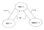
図7は、本発明の方法の図である。ハイブリッドプロセッサ111、117、116、115、114、113および107は、3区分の状態で動作する。それらは待機モード、経路指定モード、および処理モードである。一実施形態では、ハイブリッドプロセッサ107と102のそれぞれに直接接続されたクライアントプロセッサ101と106のみ、処理コマンドワードを出すことによって待機モードから処理モードへの移行が可能になる。しかし任意のポートで表示される経路指定コマンドワードは、待機モードから経路指定モードへの移行をもたらす。処理モードまたは経路指定モードから待機モードへ戻るための移行は、ハイブリッドプロセッサの厳格な制御下にある。
FIG. 7 is a diagram of the method of the present invention. The
以上で説明された発明の実施形態に従って、RCWとPCWの1ワードを使用した方法により、クライアントプロセッサと外部メモリ装置または直列のインタフェース間、クライアントプロセッサとハイブリッドプロセッサのペア間の通信ができる。代替の実施形態で、2つの連続して組み合わされた経路指定のコマンドワードおよび処理のコマンドワードを使用した改良方法により、マルチプロセッサアレイのすべてのプロセッサ間で互いに外部装置とインタフェースを用いて通信ができ、送受信プロセッサのアドレス、経路指定のワードカウント、処理のワードカウントを含むためのフォーマットに適応する改良を用いて、RモードとPモードの切り替えができることが当業者によって認識されるだろう。さらに代替の実施形態では、組み合わされた経路指定コマンドおよび処理のコマンドは、18ビットより大きい1ワードを使用できるか、またはその組み合わされたコマンドは、2ワード以上備えることができる。 According to the embodiment of the present invention described above, communication between a client processor and an external memory device or a serial interface and between a client processor and a hybrid processor pair can be performed by a method using one word of RCW and PCW. In an alternative embodiment, an improved method using two consecutively combined routing and processing command words allows all processors in the multiprocessor array to communicate with each other using external devices and interfaces. It will be appreciated by those skilled in the art that the R mode and P mode can be switched with improvements adapted to the format to include the transmit / receive processor address, routing word count, and processing word count. In a further alternative embodiment, the combined routing and processing commands can use one word greater than 18 bits, or the combined command can comprise more than one word.
各種改良は、その値または範囲を変えることなく本発明に対して行うことができる。この発明は例えば、本明細書で特定のプロセッサ101−124の例を用いて説明したが、多数のまたはすべての発明の態様は、他のコンピュータ設計、他の種類のコンピュータアレイ等に容易に適応できる。 Various modifications can be made to the invention without changing its value or range. Although the invention has been described herein using, for example, specific processor 101-124 examples, many or all aspects of the invention can be readily adapted to other computer designs, other types of computer arrays, and the like. it can.
同様に本発明では、主に1つのダイ上のアレイ100でプロセッサ101-124間の通信に関して本明細書で説明したが、同じ方式および方法または改良を用いて、プロセッサ101−124と外部メモリ131との間、またはアレイ100のプロセッサ101−124と外部装置133との間の通信等の他のデバイス間通信を行うことができる。
Similarly, although the present invention has been described herein primarily with respect to communication between processors 101-124 in
発明のアレイ100の具体例、プロセッサ101−124、関連装置、および方法を本明細書で説明したが、これらに対するまだ計画されていない用途が数多くあることが予想される。実際、発明の方法および装置を多種多様の用途に適用できることは、本発明の利点の一つである。
Although embodiments of the
上記の全ては、本発明の利用可能な実施形態の一部にすぎない。発明の精神と範囲から逸脱することなく、多数の他の改良および代替を行うことができることを当業者は容易に推察するだろう。よって本明細書の開示は、限定を意図するものではなく、添付の請求は本発明の全範囲を網羅するものとして解釈される。 All of the above are only some of the available embodiments of the present invention. Those skilled in the art will readily appreciate that numerous other modifications and alternatives can be made without departing from the spirit and scope of the invention. Accordingly, the disclosure herein is not intended to be limiting and the appended claims are to be construed as covering the full scope of the invention.
発明したコンピュータアレイ100、プロセッサ101−124、リンク200、データ回線210、制御回線215、PCW(Process Command Words)、RCW(Routing Connection Words)、およびそれらの方法は、多種多様のコンピュータ用途に幅広く使用されることを目的としている。それらは、かなりの演算能力を必要とし、その上消費電力および熱発生量が重視される用途で特に役立つことが予想される。
The invented
本明細書で上記に説明したように、本発明の適用性は、アレイのコンピュータ間の情報および資源の共用によりスピードと多様性の両方が非常に強化されたことである。コンピュータアレイと他の装置間の通信もまた、説明された方法と手段に従って強化された。コンピュータアレイ100、プロセッサ101−124、リンク200、データ回線210、制御回線215、PCW(Process Command Words)、RCW(Routing Connection Words)、および本発明の方法は、容易に作成でき、従来のタスク、入力/出力装置等と統合でき、本明細書で説明した利点が提供されことで、産業で容易に認められることが予想される。これらと他の理由により、発明の実用性および産業上の利用性はその範囲において重要であり、その期間において長続きすることが予想される。
As explained hereinabove, the applicability of the present invention is that both speed and diversity are greatly enhanced by the sharing of information and resources between the computers of the array. Communication between the computer array and other devices was also enhanced according to the methods and means described.
100 マルチプロセッサアレイ
101−124 プロセッサ
131,132 外部入力/出力(i/o)接続
133,134 外部装置
200 リンク
210 データ回線
215 制御回線
100 Multiprocessor array 101-124
Claims (17)
各プロセッサは、2つのみのプロセッサに接続されているリンクによって、少なくとも2つの隣接プロセッサに接続され、
前記複数のプロセッサは、前記リンクの命令を受信すると待機モードとアクティブモードとの間で切り替え可能であることを特徴とするコンピュータアレイ。 A computer array comprising a plurality of processors,
Each processor is connected to at least two neighboring processors by a link connected to only two processors,
The computer array, wherein the plurality of processors are switchable between a standby mode and an active mode upon receiving the link command.
前記アレイの各角の前記プロセッサは、前記アレイの端部の前記2つのプロセッサに接続している2つの付随リンクを有し、
4つのプロセッサにつながる4つのリンクによって接続された複数のハイブリッドプロセッサをさらに備え、
前記アレイの端部でも角でもないプロセッサに接続された前記端部のプロセッサの前記リンクは、1つのハイブリッドプロセッサに接続されている、ことを特徴とする請求項1ないし4のいずれかに記載のコンピュータアレイ。 The plurality of processors at the end of the array have three links connected to three adjacent processors;
The processor at each corner of the array has two associated links connected to the two processors at the end of the array;
A plurality of hybrid processors connected by four links leading to the four processors;
5. The link of any of the end processors connected to a processor that is neither an end nor a corner of the array is connected to a single hybrid processor. Computer array.
前記プロセッサを2つの直接隣接するプロセッサに接続するために少なくとも2つのリンクに接続するように適用された中央処理装置と、
前記中央処理装置に接続されたメモリ装置とを備え、
前記リンクのどちらかの命令により、前記中央処理装置を待機モードからアクティブモードにシフトさせることを特徴とするコンピュータアレイで使用するプロセッサ。 A processor for use in a computer array,
A central processing unit adapted to connect to at least two links to connect the processor to two immediately adjacent processors;
A memory device connected to the central processing unit,
A processor for use in a computer array, wherein the central processing unit is shifted from a standby mode to an active mode by an instruction of either of the links.
前記アレイの一部のプロセッサを、少なくとも待機モードおよびタスクを実行する別のモードを有するマルチモードプロセッサとして指定するステップと、
コマンドワードを受信すると前記指定されたプロセッサを前記他のモードに切り替えるステップと、
前記コマンドワードを受信するとタスクを行うステップと、
前記タスクが終了すると再び待機モードに切り替わるステップと
を備えたことを特徴とするマルチプロセッサアレイを動作させる方法。 A method of operating a multiprocessor array comprising:
Designating some processors of the array as multi-mode processors having at least a standby mode and another mode for performing tasks;
Switching the designated processor to the other mode upon receipt of a command word;
Performing a task upon receipt of the command word;
And a step of switching to the standby mode again when the task is completed.
経路指定タスクまたは処理タスクを行うステップと、
前記タスクが終了すると待機モードに戻るステップと
を備えたことを特徴とする請求項16に記載のマルチプロセッサアレイを動作させる方法。 Switching the designated processor to a routing mode or processing mode upon receipt of a routing word or processing command word;
Performing a routing or processing task;
The method of operating a multiprocessor array according to claim 16, further comprising the step of returning to a standby mode when the task is completed.
Applications Claiming Priority (1)
| Application Number | Priority Date | Filing Date | Title |
|---|---|---|---|
| US11/809,197 US7840826B2 (en) | 2007-05-31 | 2007-05-31 | Method and apparatus for using port communications to switch processor modes |
Publications (1)
| Publication Number | Publication Date |
|---|---|
| JP2009059346A true JP2009059346A (en) | 2009-03-19 |
Family
ID=39628784
Family Applications (1)
| Application Number | Title | Priority Date | Filing Date |
|---|---|---|---|
| JP2008139702A Pending JP2009059346A (en) | 2007-05-31 | 2008-05-28 | Method and device for connecting with a plurality of multimode processors |
Country Status (7)
| Country | Link |
|---|---|
| US (1) | US7840826B2 (en) |
| EP (1) | EP1998258A1 (en) |
| JP (1) | JP2009059346A (en) |
| KR (1) | KR20080106129A (en) |
| CN (1) | CN101320363A (en) |
| TW (1) | TW200846923A (en) |
| WO (1) | WO2008153817A2 (en) |
Families Citing this family (6)
| Publication number | Priority date | Publication date | Assignee | Title |
|---|---|---|---|---|
| US8869299B2 (en) * | 2009-03-04 | 2014-10-21 | Titus Inc. | Method and system for generating trusted security labels for electronic documents |
| US8407805B2 (en) | 2009-03-04 | 2013-03-26 | Titus Inc. | Method and system for classifying and redacting segments of electronic documents |
| US8332350B2 (en) | 2009-04-08 | 2012-12-11 | Titus Inc. | Method and system for automated security access policy for a document management system |
| CN102105866B (en) * | 2009-05-25 | 2014-02-26 | 松下电器产业株式会社 | Multiprocessor system, multiprocessor control method, and multiprocessor integrated circuit |
| US9553762B1 (en) | 2014-06-26 | 2017-01-24 | Altera Corporation | Network-on-chip with fixed and configurable functions |
| US11960438B2 (en) | 2020-09-08 | 2024-04-16 | Rambus Inc. | Methods and circuits for streaming data to processing elements in stacked processor-plus-memory architecture |
Family Cites Families (13)
| Publication number | Priority date | Publication date | Assignee | Title |
|---|---|---|---|---|
| US5251299A (en) * | 1985-12-28 | 1993-10-05 | Fujitsu Limited | System for switching between processors in a multiprocessor system |
| US5396635A (en) * | 1990-06-01 | 1995-03-07 | Vadem Corporation | Power conservation apparatus having multiple power reduction levels dependent upon the activity of the computer system |
| US5367636A (en) * | 1990-09-24 | 1994-11-22 | Ncube Corporation | Hypercube processor network in which the processor indentification numbers of two processors connected to each other through port number n, vary only in the nth bit |
| CA2073516A1 (en) * | 1991-11-27 | 1993-05-28 | Peter Michael Kogge | Dynamic multi-mode parallel processor array architecture computer system |
| US6898721B2 (en) * | 2001-06-22 | 2005-05-24 | Gallitzin Allegheny Llc | Clock generation systems and methods |
| AU2002360469A1 (en) | 2001-12-06 | 2003-06-23 | University Of Georgia Research Foundation, Inc. | Floating point intensive reconfigurable computing system for iterative applications |
| US7505413B2 (en) * | 2004-09-09 | 2009-03-17 | Cariden Technologies, Inc. | Methods and systems to perform traffic engineering in a metric-routed network |
| US7152169B2 (en) * | 2002-11-29 | 2006-12-19 | Intel Corporation | Method for providing power management on multi-threaded processor by using SMM mode to place a physical processor into lower power state |
| US7496915B2 (en) * | 2003-04-24 | 2009-02-24 | International Business Machines Corporation | Dynamic switching of multithreaded processor between single threaded and simultaneous multithreaded modes |
| US7937557B2 (en) * | 2004-03-16 | 2011-05-03 | Vns Portfolio Llc | System and method for intercommunication between computers in an array |
| US20050262278A1 (en) * | 2004-05-20 | 2005-11-24 | Schmidt Dominik J | Integrated circuit with a plurality of host processor family types |
| US7904615B2 (en) * | 2006-02-16 | 2011-03-08 | Vns Portfolio Llc | Asynchronous computer communication |
| US7752422B2 (en) * | 2006-02-16 | 2010-07-06 | Vns Portfolio Llc | Execution of instructions directly from input source |
-
2007
- 2007-05-31 US US11/809,197 patent/US7840826B2/en not_active Expired - Fee Related
-
2008
- 2008-05-13 EP EP08251682A patent/EP1998258A1/en not_active Withdrawn
- 2008-05-16 TW TW097118082A patent/TW200846923A/en unknown
- 2008-05-28 JP JP2008139702A patent/JP2009059346A/en active Pending
- 2008-05-29 WO PCT/US2008/006794 patent/WO2008153817A2/en active Search and Examination
- 2008-05-30 KR KR1020080051202A patent/KR20080106129A/en not_active Application Discontinuation
- 2008-05-30 CN CNA200810098352XA patent/CN101320363A/en active Pending
Also Published As
| Publication number | Publication date |
|---|---|
| WO2008153817A2 (en) | 2008-12-18 |
| KR20080106129A (en) | 2008-12-04 |
| TW200846923A (en) | 2008-12-01 |
| US20080301482A1 (en) | 2008-12-04 |
| EP1998258A1 (en) | 2008-12-03 |
| US7840826B2 (en) | 2010-11-23 |
| CN101320363A (en) | 2008-12-10 |
| WO2008153817A3 (en) | 2009-02-26 |
Similar Documents
| Publication | Publication Date | Title |
|---|---|---|
| US8050256B1 (en) | Configuring routing in mesh networks | |
| US8045546B1 (en) | Configuring routing in mesh networks | |
| US8832413B2 (en) | Processing system with interspersed processors and communication elements having improved wormhole routing | |
| EP0726532B1 (en) | Array processor communication architecture with broadcast instructions | |
| US8058899B2 (en) | Logic cell array and bus system | |
| US5682491A (en) | Selective processing and routing of results among processors controlled by decoding instructions using mask value derived from instruction tag and processor identifier | |
| US8151088B1 (en) | Configuring routing in mesh networks | |
| EP0539595A1 (en) | Data processor and data processing method | |
| JPH07152722A (en) | Dynamically reconstitutable switching device for simd multiprocessor | |
| JPH08171537A (en) | Mesh array processor | |
| KR20010014381A (en) | Manifold array processor | |
| JPH0675986A (en) | Large scale parallel computing system device | |
| JP2009059346A (en) | Method and device for connecting with a plurality of multimode processors | |
| US7383419B2 (en) | Address generation unit for a processor | |
| US20070136560A1 (en) | Method and apparatus for a shift register based interconnection for a massively parallel processor array | |
| CN108874730B (en) | Data processor and data processing method | |
| CN100481060C (en) | Method for multi-nuclear expansion in flow processor | |
| CN112486905A (en) | Reconfigurable isomerization PEA interconnection method | |
| JP2655243B2 (en) | Complex vector parallel computer | |
| JP4212161B2 (en) | Semiconductor device | |
| JPH09179840A (en) | Inter-processor coupling network for parallel computer | |
| JPH02240765A (en) | Data communication system for computer |