JP2009026962A - Exposure apparatus, information processing apparatus and device manufacturing method - Google Patents
Exposure apparatus, information processing apparatus and device manufacturing method Download PDFInfo
- Publication number
- JP2009026962A JP2009026962A JP2007188664A JP2007188664A JP2009026962A JP 2009026962 A JP2009026962 A JP 2009026962A JP 2007188664 A JP2007188664 A JP 2007188664A JP 2007188664 A JP2007188664 A JP 2007188664A JP 2009026962 A JP2009026962 A JP 2009026962A
- Authority
- JP
- Japan
- Prior art keywords
- shot
- substrate
- layout
- surface shape
- exposure
- Prior art date
- Legal status (The legal status is an assumption and is not a legal conclusion. Google has not performed a legal analysis and makes no representation as to the accuracy of the status listed.)
- Pending
Links
Images


Classifications
-
- G—PHYSICS
- G03—PHOTOGRAPHY; CINEMATOGRAPHY; ANALOGOUS TECHNIQUES USING WAVES OTHER THAN OPTICAL WAVES; ELECTROGRAPHY; HOLOGRAPHY
- G03F—PHOTOMECHANICAL PRODUCTION OF TEXTURED OR PATTERNED SURFACES, e.g. FOR PRINTING, FOR PROCESSING OF SEMICONDUCTOR DEVICES; MATERIALS THEREFOR; ORIGINALS THEREFOR; APPARATUS SPECIALLY ADAPTED THEREFOR
- G03F7/00—Photomechanical, e.g. photolithographic, production of textured or patterned surfaces, e.g. printing surfaces; Materials therefor, e.g. comprising photoresists; Apparatus specially adapted therefor
- G03F7/70—Microphotolithographic exposure; Apparatus therefor
- G03F7/70425—Imaging strategies, e.g. for increasing throughput or resolution, printing product fields larger than the image field or compensating lithography- or non-lithography errors, e.g. proximity correction, mix-and-match, stitching or double patterning
Abstract
Description
本発明は、原版のパターンを基板に投影して該基板を露光する露光装置、露光装置において露光の際に使用されるショットレイアウトを決定する情報処理装置、該露光装置を用いてデバイスを製造するデバイス製造方法に関する。 The present invention relates to an exposure apparatus that projects an original pattern onto a substrate and exposes the substrate, an information processing apparatus that determines a shot layout used in exposure in the exposure apparatus, and a device using the exposure apparatus. The present invention relates to a device manufacturing method.
近年の回路パターンの微細化及び高密度化の要請から、半導体デバイスを製造するための投影露光装置には、原版(マスク又はレチクルと呼ばれうる)に形成された回路パターンを基板(例えばウエハ)により高い解像力で投影することが要求されている。一方で、高い生産性を得る為に、単位時間あたりに処理可能な基板の枚数で表されうる処理性能(スループット)の向上も求められている。半導体製造装置にとって精度とスループットは一般に相反する性能であり、精度を上げる為に多くの計測を行うとスループットが低下しうる。精度を保ちながらスループットを向上させる技術として、次のような手法がある。 Due to the recent demand for miniaturization and high density of circuit patterns, a projection exposure apparatus for manufacturing semiconductor devices uses a circuit pattern formed on an original (which may be called a mask or a reticle) as a substrate (for example, a wafer). Therefore, it is required to project with higher resolution. On the other hand, in order to obtain high productivity, improvement in processing performance (throughput) that can be expressed by the number of substrates that can be processed per unit time is also required. Accuracy and throughput are generally contradictory performances for a semiconductor manufacturing apparatus, and if many measurements are performed to increase accuracy, the throughput may decrease. There are the following techniques as techniques for improving throughput while maintaining accuracy.
第1の手法は、計測に用いるサンプルとなるショット(以下、サンプルショット)を計測の種類ごとに最も有効な最低限数のサンプルショットとする方法である。特に、1つのレシピの中で、計測の種類毎に異なるショットレイアウトとそれに基づく有効なサンプルショットを選択しておくことで、各種計測の回数を減じる手法がとられる。 The first method is a method in which shots (hereinafter referred to as sample shots) to be samples used for measurement are the most effective minimum number of sample shots for each type of measurement. In particular, a method of reducing the number of various measurements by selecting a different shot layout for each type of measurement and an effective sample shot based on the shot layout in one recipe.
第2の手法は、1つの露光画角(ショット)を大きくとる方法である。1枚の基板あたりのショット数を減らすことは、露光装置のスループットを大きく向上させる。例えば、1つのショットで4つのチップ領域を露光することができれば、1つのショットで1つのチップの領域しか露光しない場合に比べて、スループットが向上する。 The second method is a method of increasing one exposure angle of view (shot). Reducing the number of shots per substrate greatly improves the throughput of the exposure apparatus. For example, if four chip areas can be exposed in one shot, the throughput is improved as compared with the case where only one chip area is exposed in one shot.
第3の手法は、2つのステージを用いる方法である。近年、1台の露光装置内に2つの基板ステージを搭載する場合が多くなってきている。2つの基板ステージは、一般に、計測処理と露光処理とを並行して実施するために用いられる。基板の露光処理時間が基板の計測処理に対して充分に長い場合には、基板に対して必要な様々な計測をより多く行うことができ高精度な位置合わせ等が可能になり、しかも、多くの計測を行うことによるスループットの低下を招きにくくなる。 The third method is a method using two stages. In recent years, there are many cases where two substrate stages are mounted in one exposure apparatus. The two substrate stages are generally used for performing measurement processing and exposure processing in parallel. If the exposure processing time of the substrate is long enough for the measurement processing of the substrate, it is possible to perform more necessary various measurements on the substrate, enabling highly accurate alignment, etc. This makes it difficult to cause a decrease in throughput due to the measurement.
露光装置に対して基板の露光の為に与えられる指示であるレシピについて考える。レシピの構成要素の内でも、特に、精度とスループットの両立という観点では、ショットレイアウトの指定は重要な意味を持つ。一般に、スループットを重視したショットレイアウトは、記述のとおり、ショット領域をなるべく大きくして基板あたりの露光回数が減らされる。しかしながら、基板の中央部分と周辺部分とでは、傾きが異なる場合が多く、全てを同一画角のショット領域として処理するとその傾きに追従できず、結局は使えないチップを作ってしまう場合がある。その場合、プロセスエンジニアがショットレイアウトを編集するなどして、以降のロット処理を続けることになりうる。事前に経験則からその事を知っているプロセスエンジニアは、レシピを作成する段階で、事前に、問題となりそうなショットをチップサイズに分割して作るかもしれない。 Consider a recipe that is an instruction given to an exposure apparatus for exposure of a substrate. Among the recipe components, the shot layout designation is particularly important from the viewpoint of achieving both accuracy and throughput. In general, in a shot layout that emphasizes throughput, as described, the shot area is made as large as possible to reduce the number of exposures per substrate. However, the inclination is often different between the central portion and the peripheral portion of the substrate, and if all are processed as shot regions having the same angle of view, the inclination cannot be followed, and eventually a chip that cannot be used may be produced. In that case, the process engineer can continue the subsequent lot processing by editing the shot layout. A process engineer who knows that from heuristics in advance may divide shots that are likely to be problematic into chip sizes in advance when creating a recipe.
しかしながら、ショットレイアウトの編集を行ったとしても、基板の表面形状は1枚毎に異なるので、最適ではない場合も存在しうるし、逆に、表面形状に問題がないのにショット領域を分割した場合には、スループットの低下を招く場合もあった。 However, even if the shot layout is edited, the surface shape of the substrate varies from one sheet to another, so there may be cases where it is not optimal, and conversely, when the shot area is divided even though there is no problem with the surface shape In some cases, the throughput may be reduced.
本発明は、上記の課題認識を契機としてなされたものであり、例えば、歩留まりの向上とスループットの向上の双方に適したショットレイアウトの決定技術を提供することを目的とする。 The present invention has been made in light of the above problem recognition, and an object of the present invention is to provide a shot layout determination technique suitable for both improving yield and improving throughput, for example.
本発明の第1の側面は、原版のパターンを基板に投影して該基板を露光する露光装置に係り、該露光装置は、露光すべき基板の表面形状を示す表面形状データに基づいてショットレイアウトを決定するレイアウト決定部と、前記レイアウト決定部によって決定されたショットレイアウトに従って基板を露光する露光部とを備える。 A first aspect of the present invention relates to an exposure apparatus that projects an original pattern onto a substrate to expose the substrate, and the exposure apparatus performs shot layout based on surface shape data indicating the surface shape of the substrate to be exposed. A layout deciding unit for deciding the exposure amount, and an exposure unit for exposing the substrate in accordance with the shot layout decided by the layout deciding unit.
本発明の第2の側面は、原版のパターンを基板に投影して該基板を露光する露光装置において露光の際に使用されるショットレイアウトを決定する情報処理装置に係り、前記情報処理装置は、露光すべき基板の表面形状を示す表面形状データに基づいてショットレイアウトを決定するレイアウト決定部を備える。 A second aspect of the present invention relates to an information processing apparatus that determines a shot layout used in exposure in an exposure apparatus that exposes the substrate by projecting an original pattern onto the substrate, and the information processing apparatus includes: A layout determining unit that determines a shot layout based on surface shape data indicating a surface shape of a substrate to be exposed is provided.
本発明によれば、例えば、歩留まりの向上とスループットの向上の双方に適したショットレイアウトの決定技術が提供される。 According to the present invention, for example, a shot layout determination technique suitable for both improvement in yield and improvement in throughput is provided.
以下、添付図面を参照しながら本発明の好適な実施形態を説明する。 Hereinafter, preferred embodiments of the present invention will be described with reference to the accompanying drawings.
図2は、本発明の好適な実施形態の露光装置の構成を概略的に示す図である。本発明の好適な実施形態の露光装置200は、原版のパターンを投影光学系を介して基板に投影して該基板を露光する。露光装置200は、例えば、制御部(情報処理装置)40と露光部30とを備えうる。露光装置200は、更に、原版搬送機構210と基板搬送機構211とを備えうる。
FIG. 2 is a view schematically showing a configuration of an exposure apparatus according to a preferred embodiment of the present invention. The
制御部40は、例えば、役割分担された複数のコンピュータシステムを接続して構成されうる。役割分担とは、例えば、組み込み機器の制御や、様々なサービスを提供するプロセスの実行、機器の制御やサービスの実行状況の表示といった処理の各々にコンピュータシステムを割り当てることを言う。 For example, the control unit 40 can be configured by connecting a plurality of computer systems that are assigned roles. The role assignment refers to, for example, assigning a computer system to each of processes such as control of embedded devices, execution of processes that provide various services, control of devices, and display of execution status of services.
制御部40は、露光部30、より具体的にはそれを構成する複数のコンポーネント(構成要素)の動作を制御しうる。制御部40はまた、原版搬送機構210及び基板搬送機構211を制御しうる。
The control unit 40 can control the operation of the
露光部30を構成するコンポーネントとしては、例えば、以下のコンポーネント201〜208があげられる。プリアライメントユニット202は、原版をプリアライメントする。原版アライメントユニット204は、原版(レチクル)のアライメントマークを計測して、原版ステージ(レチクルステージ)に対する原版の位置を計測する。原版ステージ203は、アライメントユニット204による原版の位置計測結果に基づいて、原版の位置ずれを補正し、原版を吸着し保持する。
Examples of the components constituting the
投影光学系205は、原版に形成されたパターンを基板(ウエハ)に投影し、これにより基板を露光する。アライメントスコープ206は、基板の位置合わせのためのアライメントマークを検出する。基板ステージ(ウエハステージ)207は、計測の際には、基板上のアライメントマークがアライメントスコープ206の視野内に入るように基板を位置決めする。基板ステージ207はまた、露光の際には、アライメントマークの計測結果に基づいて基板を位置決めする。
The projection
露光部30は、計測と露光とを並行して実施するために2つの基板ステージ207、208を備えてもよい。このような構成は、ツインステージ構成と呼ばれうる。例えば、1つの基板ステージ207を使って第1基板を露光している間に、他の基板ステージ208を使って次に露光すべき第2基板の計測を行うことができる。第1基板の露光と第2基板の計測が終了したら2つの基板ステージ207、208を入れ替えて、第2基板を露光し、その間に、第1基板を次に露光すべき第3基板に変更して第3基板の計測がなされうる。
The
露光装置200は、基板の面位置の測定するための面位置センサ209を備えている。面位置センサ209としては、例えば、斜入射方式のセンサが好適である。斜入射方式のセンサは、基板に光ビームを斜入射させ、基板で反射された光ビームが受光面に入射する位置に基づいて基板の面位置を測定する。
The
原版搬送機構210は、例えば、外部から提供された原版をプリアライメントユニット202に搬送したり、使用すみ原版を原版ステージ203から外部装置に渡すために搬送したりする。
For example, the
基板搬送機構211は、例えば、外部から提供された基板を基板ステージ207(又は208)に搬送したり、露光が完了した基板を外部装置に渡すために搬送したりする。
For example, the
以上のようなコンポーネント202〜209、原版搬送機構210、基板搬送機構211は、有線又は無線の通信手段を介して情報処理装置201と接続されている。
The
図3は、原版搬送機構210の動作を説明する図である。原版は、露光装置の外部(典型的には、ストッカ)から搬送ロボットによって露光装置の所定のポートに提供されうる。ステップ301において、その原版は、原版搬送機構210によってプリアライメントユニット202のプリアライメントステージに搬送される。
FIG. 3 is a diagram for explaining the operation of the
次いで、ステップ302において、プリアライメントユニット202によって、原版の模索マークが観察され、その模索マークが基準位置に一致するようにプリアライメントステージの位置が調整される。
Next, in
次いで、ステップ303において、プリアライメントステージ上の原版は、原版ステージ203に搬送される。
Next, in
次いで、ステップ304において、原版アライメントユニット204によって、原版のアライメントマークが観察されその結果に基づいて原版ステージが駆動されて原版と原版ステージ203との位置関係がx軸方向、y軸方向、θ(回転角度)方向に補正される。
Next, in
次いで、ステップ305において、原版が原版ステージに真空吸着によって固定される。
Next, in
図1は、露光装置200の動作を例示する図である。図1に示す処理は、制御部40によって制御される。露光装置200は、外部から搬送されてくる基板を受け取る。露光装置200に搬入される前に外部の検査装置等で基板の表面形状の計測がなされている場合は、制御部40は、その表面形状の計測結果(表面形状を示す表面形状データ)を受け取ることができる。この情報の受け取りは、例えば、基板を露光装置に接続されたCD(コータデベロッパ)からインラインで受け取る場合には、CDとのインライン信号に同期して検査装置から受け取ることができる。或いは、基板の受け取りに先立ち、又は、受け取った後に、露光装置200のオンラインIF(不図示)を介して工場側ホスト又はMC(マシンコンポーネント)から受け取ることができる。ここで、CDと露光装置の双方にオンラインIFを介してMCが接続されているのが通例である。
FIG. 1 is a diagram illustrating the operation of the
なお、ステップ101は、露光装置の外部で基板の表面形状が計測される場合にオプションで実行されうる処理である。 Step 101 is a process that can be optionally executed when the surface shape of the substrate is measured outside the exposure apparatus.
基板が露光装置200に搬入されると、ステップS102において、露光装置200のメカプリアライメントユニット(不図示)によって基板の外形基準(例えば、オリエンテーションフラット、ノッチ)が検出される。そして、その検出結果に基づいて、基板の向きがレシピで指定された向きに向くように基板の向き(θ回転角度)が調整される。その後、基板は、基板搬送機構211によって基板ステージ207の微動ステージに送り込まれる(103)。
When the substrate is carried into the
次いで、ステップ104において、基板の位置が補正される。具体的には、基板ステージ207(又は208)の微動ステージに置かれた基板のアライメントマークが観察されて基板の位置(x、y、z方向、及び、ωz方向の位置)のずれ量が検出される。そして、その検出結果に基づいて、アライメントマークがアライメントスコープ206の視野内に入るように基板ステージ207(208)の微動ステージが駆動される。
Next, in
次いで、ステップ105において、基板の傾きが補正される。この処理では、レシピで指定された複数のサンプルショットについてその中心の高さ(フォーカス位置)が面位置測定センサ(計測器)109で計測される。そして、その計測結果に基づいて基板の傾き(チルト)が算出され、その傾きを補正するように基板ステージ208の微動ステージの駆動部に指令が送られる。
Next, in
次に、基板の表面形状が計測される(106)。表面形状は、例えば、各ショットの代表位置、例えば中心位置の高さ(投影光学系205の光軸方向の位置)を計測することによってなされうる。この計測には、面位置センサ(計測器)209が使用されうる。なお、基板の表面形状が外部装置で測定される場合には、基板の表面形状データを当該外部装置から得てもよい(101)。
Next, the surface shape of the substrate is measured (106). The surface shape can be determined by, for example, measuring the representative position of each shot, for example, the height of the center position (the position of the projection
次いで、ステップ213において、制御部40は、基板の表面形状データに基づいてショットレイアウトが決定される。この決定は、制御部40のレイアウト決定部41によってなされうる。ショットレイアウトの選択の詳細については後述する。
Next, in
次いで、ステップ108において、制御部40は、複数のサンプルショットを対象として基板表面(レジスト表面)のパターン段差を求め、ショット間で共通の平均的な段差情報を算出する。このパターン段差についても、面位置センサ209を利用してなされうる。
Next, in
次いで、ステップ109において、複数のサンプルショットを対象として、ショットのx方向とy方向に各々1箇所又は数箇所に配置されたアライメントマークがアライメントスコープ206を用いて計測される。そして、その結果に基づいて基板のシフト量、回転誤差、倍率誤差、直交度、ショット倍率誤差、ショット回転誤差が決定される。
Next, in
次いで、ステップ120において、ステップ109で得られた情報(計測結果)に基づいて基板が位置決めされて該基板が露光される。基板の複数のショット領域の露光は、ステップ213で決定されたショットレイアウトに従ってなされる。
Next, in
全てのショット領域の露光を終了すると、基板搬送機構211によって基板ステージ208から露光装置200の外部に基板が搬送される。
When the exposure of all the shot areas is completed, the substrate is transported from the
図4は、2つの基板ステージ207、208を備えるツインステージ構成において露光と計測を並行して実行することを模式的に示す図である。ツインステージ構成の露光装置においては、一方の基板ステージを使って露光(120)がなされている間に、他方の基板ステージに外部装置から基板が搬送され、該他方の基板ステージを使って計測がなされる(104〜109)。その後、露光及び計測の双方が終了するまで待って(401、402)、2つの基板ステージが入れ替えられる(403)。
FIG. 4 is a diagram schematically showing that exposure and measurement are performed in parallel in a twin stage configuration including two
図7は、基板の表面形状の計測について説明する図である。ここでは、説明を簡単にするために、x座標とy座標とz値の精度は簡略化してある。単位も明確にはしていない。実際には、精度と単位はナノメートルレベルである。Z値は、基板の露光基準面(投影光学系205の像面)に対してショット領域がどの程度の高さの差を有するかを示しており、例えば、+は露光基準面に対して上方へのずれ、―は露光基準面に対して下方へのずれを示す。 FIG. 7 is a diagram for explaining the measurement of the surface shape of the substrate. Here, in order to simplify the description, the accuracy of the x coordinate, the y coordinate, and the z value is simplified. The unit is not clarified. In practice, accuracy and units are at the nanometer level. The Z value indicates how much the shot area has a difference with respect to the exposure reference plane (image plane of the projection optical system 205) of the substrate. For example, + is above the exposure reference plane. The shift to-indicates a shift downward with respect to the exposure reference plane.
基板の表面形状の計測(ステップ106)が図7(a)における黒点702、703、704やその他の黒点に対して行われたと仮定する。計測がなされた各点について、基板上でのxy座標とその点における露光基準面に対する高さ方向の差とをデータとして得ることができる。なお、基板の表面形状の計測において基板のどの部分(測定点)をいくつ測定するかについては、例えば、レシピで指定したり、基板に予め設置された測定用マークを検出することにより決定したりすることができる。露光装置の外部装置で計測がなされる場合には、ステップ101において、その計測結果を示す情報が外部装置から露光装置に提供されうる。
It is assumed that the measurement of the surface shape of the substrate (step 106) is performed on the
図4(b)は、基板の表面形状の計測結果を模式的かつ例示的に示す図である。例えば、黒点702は、基板上の(x,y)=(3,8)の位置にあり、この測定点における基板面の高さと露光基準面との高さの違いは0.1である。なお、レシピ上のショットレイアウトのデータと比較すれば、例えば、測定点702は、第1ショット706に属していることが特定される。なお、ここでは、左上から順に右下に向かって第1〜第nショットと記述している。同様に、黒点703は、基板上の(x,y)=(4,8)の位置にあり、この計測点における基板面の高さと露光基準面との高さの違いは0.2である。この計測点703は、レシピのレイアウト情報から第2ショットに属している事が特定される。なお、図7(b)には、表面形状データが24計測点分しか示されていないが、実際には、図7(a)の黒点の計測を行った場合には、68個の計測点の表面形状データが得られる。図7(b)に例示的に示す表面形状データは、ステップ101又は106において得られる。
FIG. 4B is a diagram schematically and exemplarily showing the measurement result of the surface shape of the substrate. For example, the
図5は、レイアウト決定部41(ステップ213)におけるショットレイアウトの決定処理の第1の具体例を示す図である。 FIG. 5 is a diagram illustrating a first specific example of shot layout determination processing in the layout determination unit 41 (step 213).
まず、ステップ501において、全てのショット領域の中から1つのショット領域が選択される。次いで、ステップ502において、選択されたショット領域内の段差(ショット内段差)が求められる。これはショット領域内に属する位置についての表面形状データに基づいて求めることができる。このショット内段差は、図1のステップ101又は106で得られた図7に例示するような表面形状データに基づいて求められうる。
First, in
例えば、図7に例示された計測結果(表面形状データ)によれば、ショット1(ショットNo=1のショット)のショット内段差は‐0.2〜0.1の範囲であることが解る。同様に、ショット2のショット内段差は0.1〜0.2の範囲、ショット3のショット内段差は−0.3〜0.2の範囲、ショット4のショット内段差は−0.4〜0.3の範囲である。
For example, according to the measurement result (surface shape data) illustrated in FIG. 7, it can be seen that the step difference in the shot 1 (shot No = 1 shot) is in the range of −0.2 to 0.1. Similarly, the shot inner step of
次いで、ステップ503において、前述のステップ502で求められたショット内段差が許容範囲内であるかが判断される。ショット内段差の許容範囲は、予めレシピや装置定数として与えておくことが考えられる。例えば許容範囲が0であれば、ショット1、ショット2、ショット3、ショット4は全てショット内段差が許容範囲外ということになる。例えば許容範囲が0.3以内とすればショット1とショット2はショット内段差が許容範囲内、ショット3とショット4はショット内段差が許容範囲外ということになる。なお、ここで述べたショット内段差を示す値の精度や単位は、説明の為に簡略化してあり、実際にはより精度の高い数値と単位が用いられうる。
Next, at
ショット内段差が許容範囲外であった場合には、ステップ506において、そのショット領域に含まれるチップの数が不良可能性チップ数としてカウントされる。例えば、1つのショット領域が4つのチップ領域を含む場合には、不良可能性チップ数としては、既カウント値に対して4チップ分が加算される。次いで、ステップ507において、不良可能性チップ数が許容範囲であるかが判断される。不良可能性チップ数の許容範囲については、予めレシピや装置定数として指定しておくと好ましい。不良可能性チップ数がこの指定を超えて多い場合には、ステップ508において、ショットレイアウトが変更される。
If the step in the shot is outside the allowable range, in
ステップ508におけるショットレイアウトの変更は、例えば、次のような方法に従って行なわれうる。第1の方法では、後述のように、レシピの中で、複数のショットレイアウト(例えば、スループット最重要視タイプ、スループットと精度との両立タイプと、精度重要視タイプ)をレシピにおいて定義しておく。そして、ショットレイアウトの変更の際に、例えば、スループット重要視タイプから、スループットと精度との両立タイプ、精度重要視タイプへとレイアウトを切り換えて行く方法が考えられる。各タイプのショットレイアウトの例については別途詳述する。
The shot layout change in
第2の方法では、ショットレイアウトの変更の際に新たなショットレイアウトを自動で生成する。 In the second method, a new shot layout is automatically generated when the shot layout is changed.
ステップ508が終了すると、その変更後のショットレイアウトにおいて、全てのショット領域についてショット内段差を改めて判断する必要があるので、ステップ501に戻る。
When
ステップS503でYESと判断した場合、および、ステップ507でYESと判断した場合には、ショット内段差の判定がすべてのショット領域についてなされたか否かを判断して、判定がなされていないショット領域が存在する場合にはステップ501に戻る。その場合には、ステップ501において、判定が未だなされていないショット領域が選択されて、ステップ502及びそれに続く処理が実行される。
If YES is determined in step S503, and if YES is determined in
ステップ504において、ショット内段差の判定がすべてのショット領域についてなされたと判断した場合には、ステップ505において、その時点で決定されているショットレイアウトを最終的なショットレイアウトとして決定する。
If it is determined in
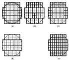
図8は、レイアウト決定部41(ステップ213)におけるショットレイアウトの決定処理において選択されうるショットレイアウトの候補を例示する図である。基板の全面に渡って1つのショットで複数のチップ領域を同時に露光することができるショットレイアウトに従って露光ができた方がショット数や計測回数を減らすことができる。したがって、そのようなショットレイアウトを採用することにより、露光装置が単位時間辺りに露光することができる基板の数(スループット)を増やすことができる。 FIG. 8 is a diagram exemplifying shot layout candidates that can be selected in the shot layout determining process in the layout determining unit 41 (step 213). The number of shots and the number of measurements can be reduced if exposure is performed according to a shot layout in which a plurality of chip regions can be exposed simultaneously with one shot over the entire surface of the substrate. Therefore, by adopting such a shot layout, the number of substrates (throughput) that the exposure apparatus can expose per unit time can be increased.
図8(d)は、1ショットで4チップを露光することができるショットレイアウトを例示している。ここでは、図8(d)に例示するショットレイアウトをスループット重要視タイプのショットレイアウトと考える。一方で、例えば基板の周辺部分は、基板の表面形状が凸凹である場合も多く、図8(a)のショットレイアウトを採用する場合が多い。図8(a)に例示されたショットレイアウトでは、基板の周辺部分のハッチング部分に基板の凸凹があることが想定されている。凸凹の多い部分ではショットをなるべく小さくし、1ショットで1チップを露光した方が不良チップを出しにくい。但し、スループットは、図8(d)に示すショットレイアウトより劣る。図8(a)に示すショットレイアウトをスループットと精度とを両立したタイプのショットレイアウトと考える。 FIG. 8D illustrates a shot layout in which four chips can be exposed in one shot. Here, the shot layout illustrated in FIG. 8D is considered to be a throughput layout type. On the other hand, for example, in the peripheral portion of the substrate, the surface shape of the substrate is often uneven, and the shot layout of FIG. In the shot layout illustrated in FIG. 8A, it is assumed that the substrate has unevenness in the hatched portion of the peripheral portion of the substrate. It is more difficult to produce a defective chip when the shot is made as small as possible in a portion with many irregularities and one chip is exposed with one shot. However, the throughput is inferior to the shot layout shown in FIG. The shot layout shown in FIG. 8A is considered as a type of shot layout that achieves both throughput and accuracy.
更に極端に安全(不良チップを出したくない)場合には、図8(e)に例示するように、ショット領域をなるべく小さくして不良チップを出しにくくするレイアウトも考えられる。但し、この場合はスループットは、図8(d)や図8(a)に対して大きく劣ることになる。図8(e)に示すショットレイアウトは、精度重要視タイプのショットレイアウトと考えることができる。 Further, in the case of extremely safety (not wanting to bring out a defective chip), as illustrated in FIG. 8E, a layout is also conceivable in which the shot area is made as small as possible to make it difficult to produce a defective chip. However, in this case, the throughput is greatly inferior to that of FIG. 8D or FIG. The shot layout shown in FIG. 8E can be considered as a precision-important shot layout.
従来は、オペレータは、レシピの中でレイアウトとして図8(d)、図8(a)、図8(e)に例示されるようなショットレイアウトの候補の中からいずれか1つののショットレイアウトを予め選択する必要があった。 Conventionally, an operator selects any one shot layout from among shot layout candidates as exemplified in FIGS. 8D, 8A, and 8E as a layout in a recipe. It was necessary to select in advance.
しかしながら、本発明の好適な実施形態によれば、基板の表面形状(より具体的な例では、ショット内段差)に基づいてショットレイアウトが個々の基板に対して決定される。 However, according to a preferred embodiment of the present invention, the shot layout is determined for each substrate based on the surface shape of the substrate (in the more specific example, the step in the shot).
次に、ショットレイアウトの変更の際に新たなショットレイアウトを自動で生成する場合に生成されうるショットレイアウトを例示的に説明する。一般に、オペレータは、経験により図8(d)、図8(a)、図8(e)に例示されるようなショットレイアウトを指定する。しかしながら、例えば基板の周辺部分に凸凹がある場合であっても、基板の周辺部部の全周にわたって凸凹があるとは限らない。そこで、図8(c)に例示するようなショットレイアウトが有効な場合もある。また、基板の中央付近等にランダムに凹凸が現れた場合には、図8(b)のようなショットレイアウトが最適である場合もあるかもしれない。 Next, a shot layout that can be generated when a new shot layout is automatically generated when the shot layout is changed will be described as an example. Generally, the operator designates a shot layout as exemplified in FIG. 8D, FIG. 8A, and FIG. However, for example, even if there are irregularities in the peripheral part of the substrate, the irregularities are not always present over the entire circumference of the peripheral part of the substrate. Therefore, a shot layout as illustrated in FIG. 8C may be effective. If irregularities appear randomly near the center of the substrate, the shot layout as shown in FIG. 8B may be optimal.
しかしながら、図8(c)や図8(b)に例示されるようなショットレイアウトは、オペレータが予め指定できるものではなく、個々基板の表面形状の計測を通して個別に生成されるべきものである。 However, shot layouts as exemplified in FIG. 8C and FIG. 8B cannot be designated in advance by an operator, and should be generated individually through measurement of the surface shape of each substrate.
図6は、レイアウト決定部41(ステップ213)におけるショットレイアウトの決定処理の第2の具体例を示す図である。この処理では、ショットレイアウトの変更の際に個別の基板の表面形状に基づいて新たなショットレイアウトが自動で生成される。図6に示す処理は、図5に示す処理のステップ508をステップ605で置き換えたものである。
FIG. 6 is a diagram illustrating a second specific example of shot layout determination processing in the layout determination unit 41 (step 213). In this process, a new shot layout is automatically generated based on the surface shape of an individual substrate when the shot layout is changed. The process shown in FIG. 6 is obtained by replacing
ステップ605では、ステップ507で不良可能性チップ数が許容範囲を超えたと判断した場合に、ステップ503でショット内段差が許容範囲を超えると判断されたショット領域をチップレベルに分割する。或いは、当該ショット領域は、2以上のチップ領域を含むより小さいショット領域に分割されてもよい。
In
例えば、初めに与えられていたショットレイアウトが図8(d)であった場合で、ショット内段差が許容範囲内ではないショット領域がステップ503において、ショット1、ショット2、ショット3、ショット4とショット12であると判断された場合を考える。この場合、該当ショット領域をチップレベルに分割すると、図8(b)に例示するようなショットレイアウトになる。
For example, in the case where the shot layout originally given is FIG. 8D, the shot areas where the step difference in the shot is not within the allowable range are shot 1, shot 2, shot 3, shot 4 in
他の例として、初めに図8の(d)の様なショットレイアウトが与えられていて、ショット内段差が許容範囲内ではないショット領域がステップ503においてショット1〜4、5、9、10、14であると判断された場合を考える。この場合、該当ショット領域をチップレベルに分割すると図8(c)に例示するようなショットレイアウトになる。以上のように、図6に例示する処理では、ショット領域をチップレベル(又は、2以上のチップ領域を含むより小さいショット領域)に分割する。
As another example, a shot region as shown in FIG. 8D is first given, and shot areas in which the step difference in the shot is not within the allowable range are
[応用例]
次に上記の露光装置を利用したデバイス製造方法を説明する。図9は、半導体デバイスの全体的な製造プロセスのフローを示す図である。ステップ1(回路設計)では半導体デバイスの回路設計を行う。ステップ2(レチクル作製)では設計した回路パターンに基づいてレチクル(原版またはマスクともいう)を作製する。一方、ステップ3(ウエハ製造)ではシリコン等の材料を用いてウエハ(基板ともいう)を製造する。ステップ4(ウエハプロセス)は前工程と呼ばれ、上記のレチクルとウエハを用いて、リソグラフィー技術によってウエハ上に実際の回路を形成する。次のステップ5(組み立て)は後工程と呼ばれ、ステップ4によって作製されたウエハを用いて半導体チップ化する工程であり、アッセンブリ工程(ダイシング、ボンディング)、パッケージング工程(チップ封入)等の組み立て工程を含む。ステップ6(検査)ではステップ5で作製された半導体デバイスの動作確認テスト、耐久性テスト等の検査を行う。こうした工程を経て半導体デバイスが完成し、これを出荷(ステップ7)する。
[Application example]
Next, a device manufacturing method using the above exposure apparatus will be described. FIG. 9 is a diagram showing a flow of an entire manufacturing process of a semiconductor device. In step 1 (circuit design), a semiconductor device circuit is designed. In step 2 (reticle fabrication), a reticle (also referred to as an original or a mask) is fabricated based on the designed circuit pattern. On the other hand, in step 3 (wafer manufacture), a wafer (also referred to as a substrate) is manufactured using a material such as silicon. Step 4 (wafer process) is called a pre-process, and an actual circuit is formed on the wafer by lithography using the reticle and wafer. The next step 5 (assembly) is called a post-process, and is a process for forming a semiconductor chip using the wafer produced in step 4, and is an assembly process (dicing, bonding), packaging process (chip encapsulation), etc. Process. In step 6 (inspection), the semiconductor device manufactured in
図10は、上記ウエハプロセスの詳細なフローを示す図である。ステップ11(酸化)ではウエハの表面を酸化させる。ステップ12(CVD)ではウエハ表面に絶縁膜を成膜する。ステップ13(電極形成)ではウエハ上に電極を蒸着によって形成する。ステップ14(イオン打込み)ではウエハにイオンを打ち込む。ステップ15(CMP)ではCMP工程によって絶縁膜を平坦化する。ステップ16(レジスト処理)ではウエハに感光剤を塗布する。ステップ17(露光)では上記の露光装置を用いて、回路パターンが形成されたマスクを介し感光剤が塗布されたウエハを露光してレジストに潜像パターンを形成する。ステップ18(現像)ではウエハ上のレジストに形成された潜像パターンを現像してレジストパターンを形成する。ステップ19(エッチング)ではレジストパターンが開口した部分を通してレジストパターンの下にある層又は基板をエッチングする。ステップ20(レジスト剥離)ではエッチングが済んで不要となったレジストを取り除く。これらのステップを繰り返し行うことによって、ウエハ上に多重に回路パターンを形成する。 FIG. 10 is a diagram showing a detailed flow of the wafer process. In step 11 (oxidation), the wafer surface is oxidized. In step 12 (CVD), an insulating film is formed on the wafer surface. In step 13 (electrode formation), an electrode is formed on the wafer by vapor deposition. In step 14 (ion implantation), ions are implanted into the wafer. In step 15 (CMP), the insulating film is planarized by a CMP process. In step 16 (resist process), a photosensitive agent is applied to the wafer. In step 17 (exposure), the above exposure apparatus is used to expose a wafer coated with a photosensitive agent through a mask on which a circuit pattern is formed, thereby forming a latent image pattern on the resist. In step 18 (development), the latent image pattern formed on the resist on the wafer is developed to form a resist pattern. In step 19 (etching), the layer or substrate under the resist pattern is etched through the portion where the resist pattern is opened. In step 20 (resist stripping), the resist that has become unnecessary after etching is removed. By repeating these steps, multiple circuit patterns are formed on the wafer.
Claims (9)
露光すべき基板の表面形状を示す表面形状データに基づいてショットレイアウトを決定するレイアウト決定部と、
前記レイアウト決定部によって決定されたショットレイアウトに従って基板を露光する露光部と、
を備えることを特徴とする露光装置。 An exposure apparatus that projects an original pattern onto a substrate to expose the substrate,
A layout determining unit that determines a shot layout based on surface shape data indicating a surface shape of a substrate to be exposed;
An exposure unit that exposes the substrate according to the shot layout determined by the layout determination unit;
An exposure apparatus comprising:
露光すべき基板の表面形状を示す表面形状データに基づいてショットレイアウトを決定するレイアウト決定部を備えることを特徴とする情報処理装置。 An information processing apparatus for determining a shot layout used in exposure in an exposure apparatus that exposes the substrate by projecting an original pattern onto the substrate,
An information processing apparatus comprising: a layout determining unit that determines a shot layout based on surface shape data indicating a surface shape of a substrate to be exposed.
請求項1乃至5のいずれか1項に記載の露光装置を用いて基板を露光する工程と、
該基板を現像する工程と、
を含むことを特徴とするデバイス製造方法。 A device manufacturing method comprising:
A step of exposing the substrate using the exposure apparatus according to claim 1;
Developing the substrate;
A device manufacturing method comprising:
Priority Applications (2)
| Application Number | Priority Date | Filing Date | Title |
|---|---|---|---|
| JP2007188664A JP2009026962A (en) | 2007-07-19 | 2007-07-19 | Exposure apparatus, information processing apparatus and device manufacturing method |
| US12/174,915 US8212990B2 (en) | 2007-07-19 | 2008-07-17 | Exposure apparatus, information processing apparatus, and method of manufacturing device |
Applications Claiming Priority (1)
| Application Number | Priority Date | Filing Date | Title |
|---|---|---|---|
| JP2007188664A JP2009026962A (en) | 2007-07-19 | 2007-07-19 | Exposure apparatus, information processing apparatus and device manufacturing method |
Publications (2)
| Publication Number | Publication Date |
|---|---|
| JP2009026962A true JP2009026962A (en) | 2009-02-05 |
| JP2009026962A5 JP2009026962A5 (en) | 2010-09-02 |
Family
ID=40346176
Family Applications (1)
| Application Number | Title | Priority Date | Filing Date |
|---|---|---|---|
| JP2007188664A Pending JP2009026962A (en) | 2007-07-19 | 2007-07-19 | Exposure apparatus, information processing apparatus and device manufacturing method |
Country Status (2)
| Country | Link |
|---|---|
| US (1) | US8212990B2 (en) |
| JP (1) | JP2009026962A (en) |
Cited By (2)
| Publication number | Priority date | Publication date | Assignee | Title |
|---|---|---|---|---|
| KR20150135089A (en) * | 2014-05-22 | 2015-12-02 | 캐논 가부시끼가이샤 | Exposure apparatus, exposure method, and device manufacturing method |
| JP2016046329A (en) * | 2014-08-20 | 2016-04-04 | キヤノン株式会社 | Lithographic device, article manufacturing method, information processing device and determining method |
Citations (6)
| Publication number | Priority date | Publication date | Assignee | Title |
|---|---|---|---|---|
| JPH07283106A (en) * | 1994-04-07 | 1995-10-27 | Rohm Co Ltd | Aligner and exposure method |
| JP2002319530A (en) * | 2001-04-20 | 2002-10-31 | Matsushita Electric Ind Co Ltd | Aligner and exposure method |
| JP2003188089A (en) * | 2001-12-21 | 2003-07-04 | Canon Inc | Method and program for calculating exposure condition, recording medium, method for manufacturing reticle, method and device for manufacturing structure, and method for providing calculation service of exposure condition |
| JP2004281434A (en) * | 2003-03-12 | 2004-10-07 | Toshiba Corp | Method of drawing up shot map, method for exposure, processor, and method and program for manufacturing semiconductor device |
| JP2005236296A (en) * | 2004-02-18 | 2005-09-02 | Asml Netherlands Bv | Lithography device executing feed-forward focus control, and method of manufacturing device |
| JP2006179889A (en) * | 2005-11-30 | 2006-07-06 | Hitachi Ltd | Method and apparatus for inspecting circuit pattern |
-
2007
- 2007-07-19 JP JP2007188664A patent/JP2009026962A/en active Pending
-
2008
- 2008-07-17 US US12/174,915 patent/US8212990B2/en not_active Expired - Fee Related
Patent Citations (6)
| Publication number | Priority date | Publication date | Assignee | Title |
|---|---|---|---|---|
| JPH07283106A (en) * | 1994-04-07 | 1995-10-27 | Rohm Co Ltd | Aligner and exposure method |
| JP2002319530A (en) * | 2001-04-20 | 2002-10-31 | Matsushita Electric Ind Co Ltd | Aligner and exposure method |
| JP2003188089A (en) * | 2001-12-21 | 2003-07-04 | Canon Inc | Method and program for calculating exposure condition, recording medium, method for manufacturing reticle, method and device for manufacturing structure, and method for providing calculation service of exposure condition |
| JP2004281434A (en) * | 2003-03-12 | 2004-10-07 | Toshiba Corp | Method of drawing up shot map, method for exposure, processor, and method and program for manufacturing semiconductor device |
| JP2005236296A (en) * | 2004-02-18 | 2005-09-02 | Asml Netherlands Bv | Lithography device executing feed-forward focus control, and method of manufacturing device |
| JP2006179889A (en) * | 2005-11-30 | 2006-07-06 | Hitachi Ltd | Method and apparatus for inspecting circuit pattern |
Cited By (4)
| Publication number | Priority date | Publication date | Assignee | Title |
|---|---|---|---|---|
| KR20150135089A (en) * | 2014-05-22 | 2015-12-02 | 캐논 가부시끼가이샤 | Exposure apparatus, exposure method, and device manufacturing method |
| JP2015222773A (en) * | 2014-05-22 | 2015-12-10 | キヤノン株式会社 | Exposure device, exposure method and method of manufacturing device |
| KR101879263B1 (en) * | 2014-05-22 | 2018-07-17 | 캐논 가부시끼가이샤 | Exposure apparatus, exposure method, and device manufacturing method |
| JP2016046329A (en) * | 2014-08-20 | 2016-04-04 | キヤノン株式会社 | Lithographic device, article manufacturing method, information processing device and determining method |
Also Published As
| Publication number | Publication date |
|---|---|
| US8212990B2 (en) | 2012-07-03 |
| US20090040480A1 (en) | 2009-02-12 |
Similar Documents
| Publication | Publication Date | Title |
|---|---|---|
| JP5096965B2 (en) | Alignment method, alignment apparatus, exposure method, and device manufacturing method | |
| JP4794882B2 (en) | Scanning exposure apparatus and scanning exposure method | |
| JP4710827B2 (en) | Alignment condition determination method and apparatus, and exposure method and apparatus | |
| US7718327B2 (en) | Overlay management method and apparatus, processing apparatus, measurement apparatus and exposure apparatus, device manufacturing system and device manufacturing method, and program and information recording medium | |
| JP2004006527A (en) | Position detection device and position detection method, exposure device, and device manufacturing method and substrate | |
| JP2018081281A (en) | Exposure equipment, exposure method, and production method of article | |
| KR101867648B1 (en) | Method of obtaining position, exposure method, and method of manufacturing article | |
| JP2006344739A (en) | Position measuring device and its method | |
| JP2009200122A (en) | Exposure system and process for fabricating device | |
| EP1372041A2 (en) | Control of an apparatus for exposing a semiconductor device | |
| JP2009130184A (en) | Alignment method, exposure method, pattern forming method and exposure device | |
| JP2002334826A (en) | Exposure method, surface-aligning method, aligner and manufacturing method of device | |
| US7212286B2 (en) | Aligning method, exposure method, exposure apparatus, and device manufacturing method | |
| JP2007311580A (en) | Exposure method, exposure device, measuring method, and measuring instrument | |
| JP7330777B2 (en) | STAGE DEVICE, CONTROL METHOD, SUBSTRATE PROCESSING APPARATUS, AND PRODUCT MANUFACTURING METHOD | |
| JP3913151B2 (en) | Method and system for optimizing parameter values of exposure apparatus, exposure apparatus and exposure method | |
| JP2009026962A (en) | Exposure apparatus, information processing apparatus and device manufacturing method | |
| WO2004092865A2 (en) | Selection method, exposure method, selection device, exposure device, and device manufacturing method | |
| JP5084432B2 (en) | Exposure method, exposure apparatus, and device manufacturing method | |
| JP3815759B2 (en) | Detection method, exposure apparatus, and device manufacturing method | |
| KR20080078585A (en) | Exposure apparatus, method of manufacturing device, method applied to exposure apparatus and computer-readable medium | |
| TWI820371B (en) | Inspection tool for use in lithographic device manufacturing processes and metrology method | |
| EP3376287A1 (en) | Methods of determining corrections for a patterning process, device manufacturing method, control system for a lithographic apparatus and lithographic apparatus | |
| JP2006148013A (en) | Positioning method and exposing method | |
| JP2000306822A (en) | Manufacture of semiconductor device |
Legal Events
| Date | Code | Title | Description |
|---|---|---|---|
| A521 | Request for written amendment filed |
Free format text: JAPANESE INTERMEDIATE CODE: A523 Effective date: 20100715 |
|
| A621 | Written request for application examination |
Free format text: JAPANESE INTERMEDIATE CODE: A621 Effective date: 20100715 |
|
| A977 | Report on retrieval |
Free format text: JAPANESE INTERMEDIATE CODE: A971007 Effective date: 20120224 |
|
| A131 | Notification of reasons for refusal |
Free format text: JAPANESE INTERMEDIATE CODE: A131 Effective date: 20120302 |
|
| A521 | Request for written amendment filed |
Free format text: JAPANESE INTERMEDIATE CODE: A523 Effective date: 20120425 |
|
| A02 | Decision of refusal |
Free format text: JAPANESE INTERMEDIATE CODE: A02 Effective date: 20120709 |