JP2009003436A - Liquid crystal display device - Google Patents
Liquid crystal display device Download PDFInfo
- Publication number
- JP2009003436A JP2009003436A JP2008127961A JP2008127961A JP2009003436A JP 2009003436 A JP2009003436 A JP 2009003436A JP 2008127961 A JP2008127961 A JP 2008127961A JP 2008127961 A JP2008127961 A JP 2008127961A JP 2009003436 A JP2009003436 A JP 2009003436A
- Authority
- JP
- Japan
- Prior art keywords
- display panel
- display
- wiring
- terminal
- circuit
- Prior art date
- Legal status (The legal status is an assumption and is not a legal conclusion. Google has not performed a legal analysis and makes no representation as to the accuracy of the status listed.)
- Withdrawn
Links
Images


Classifications
-
- G—PHYSICS
- G02—OPTICS
- G02F—OPTICAL DEVICES OR ARRANGEMENTS FOR THE CONTROL OF LIGHT BY MODIFICATION OF THE OPTICAL PROPERTIES OF THE MEDIA OF THE ELEMENTS INVOLVED THEREIN; NON-LINEAR OPTICS; FREQUENCY-CHANGING OF LIGHT; OPTICAL LOGIC ELEMENTS; OPTICAL ANALOGUE/DIGITAL CONVERTERS
- G02F1/00—Devices or arrangements for the control of the intensity, colour, phase, polarisation or direction of light arriving from an independent light source, e.g. switching, gating or modulating; Non-linear optics
- G02F1/01—Devices or arrangements for the control of the intensity, colour, phase, polarisation or direction of light arriving from an independent light source, e.g. switching, gating or modulating; Non-linear optics for the control of the intensity, phase, polarisation or colour
- G02F1/13—Devices or arrangements for the control of the intensity, colour, phase, polarisation or direction of light arriving from an independent light source, e.g. switching, gating or modulating; Non-linear optics for the control of the intensity, phase, polarisation or colour based on liquid crystals, e.g. single liquid crystal display cells
- G02F1/133—Constructional arrangements; Operation of liquid crystal cells; Circuit arrangements
- G02F1/1333—Constructional arrangements; Manufacturing methods
- G02F1/1345—Conductors connecting electrodes to cell terminals
- G02F1/13452—Conductors connecting driver circuitry and terminals of panels
-
- G—PHYSICS
- G02—OPTICS
- G02F—OPTICAL DEVICES OR ARRANGEMENTS FOR THE CONTROL OF LIGHT BY MODIFICATION OF THE OPTICAL PROPERTIES OF THE MEDIA OF THE ELEMENTS INVOLVED THEREIN; NON-LINEAR OPTICS; FREQUENCY-CHANGING OF LIGHT; OPTICAL LOGIC ELEMENTS; OPTICAL ANALOGUE/DIGITAL CONVERTERS
- G02F1/00—Devices or arrangements for the control of the intensity, colour, phase, polarisation or direction of light arriving from an independent light source, e.g. switching, gating or modulating; Non-linear optics
- G02F1/01—Devices or arrangements for the control of the intensity, colour, phase, polarisation or direction of light arriving from an independent light source, e.g. switching, gating or modulating; Non-linear optics for the control of the intensity, phase, polarisation or colour
- G02F1/13—Devices or arrangements for the control of the intensity, colour, phase, polarisation or direction of light arriving from an independent light source, e.g. switching, gating or modulating; Non-linear optics for the control of the intensity, phase, polarisation or colour based on liquid crystals, e.g. single liquid crystal display cells
- G02F1/133—Constructional arrangements; Operation of liquid crystal cells; Circuit arrangements
- G02F1/1333—Constructional arrangements; Manufacturing methods
- G02F1/133342—Constructional arrangements; Manufacturing methods for double-sided displays
-
- G—PHYSICS
- G02—OPTICS
- G02F—OPTICAL DEVICES OR ARRANGEMENTS FOR THE CONTROL OF LIGHT BY MODIFICATION OF THE OPTICAL PROPERTIES OF THE MEDIA OF THE ELEMENTS INVOLVED THEREIN; NON-LINEAR OPTICS; FREQUENCY-CHANGING OF LIGHT; OPTICAL LOGIC ELEMENTS; OPTICAL ANALOGUE/DIGITAL CONVERTERS
- G02F1/00—Devices or arrangements for the control of the intensity, colour, phase, polarisation or direction of light arriving from an independent light source, e.g. switching, gating or modulating; Non-linear optics
- G02F1/01—Devices or arrangements for the control of the intensity, colour, phase, polarisation or direction of light arriving from an independent light source, e.g. switching, gating or modulating; Non-linear optics for the control of the intensity, phase, polarisation or colour
- G02F1/13—Devices or arrangements for the control of the intensity, colour, phase, polarisation or direction of light arriving from an independent light source, e.g. switching, gating or modulating; Non-linear optics for the control of the intensity, phase, polarisation or colour based on liquid crystals, e.g. single liquid crystal display cells
- G02F1/133—Constructional arrangements; Operation of liquid crystal cells; Circuit arrangements
- G02F1/1333—Constructional arrangements; Manufacturing methods
- G02F1/1345—Conductors connecting electrodes to cell terminals
Landscapes
- Physics & Mathematics (AREA)
- Nonlinear Science (AREA)
- Mathematical Physics (AREA)
- Chemical & Material Sciences (AREA)
- Crystallography & Structural Chemistry (AREA)
- General Physics & Mathematics (AREA)
- Optics & Photonics (AREA)
- Liquid Crystal (AREA)
- Control Of Indicators Other Than Cathode Ray Tubes (AREA)
- Devices For Indicating Variable Information By Combining Individual Elements (AREA)
Abstract
Description
本発明は、物、方法、または、物を生産する方法に関する。特に、表示装置または半導体装置に関する。 The present invention relates to an object, a method, or a method for producing an object. In particular, the present invention relates to a display device or a semiconductor device.
携帯電話機等の電子機器の画像表示部には、液晶パネルを用いて画像を表示する液晶表示モジュールが使用されている。他にも、液晶パネルに替えて有機エレクトロルミネッセンス(有機EL)パネルを用いた表示モジュールの実用化も進められている。 A liquid crystal display module that displays an image using a liquid crystal panel is used in an image display unit of an electronic device such as a mobile phone. In addition, a display module using an organic electroluminescence (organic EL) panel instead of a liquid crystal panel has been put into practical use.
表示モジュールは、液晶や有機EL素子で形成される表示パネルと、ドライバICや電源ICが実装された回路基板とをフレキシブル配線基板で連結して構成されている。フレキシブル配線基板は樹脂フィルムの上に配線パターンを形成したものであり、この上にドライバICを直接実装したものも用いられている。 The display module is configured by connecting a display panel formed of a liquid crystal or an organic EL element and a circuit board on which a driver IC and a power supply IC are mounted with a flexible wiring board. The flexible wiring board has a wiring pattern formed on a resin film, and a driver IC directly mounted thereon is also used.
ところで、携帯電話機等の電子機器は高機能化が進み、折り畳み式の筐体の表裏にメイン画面とサブ画面を設け、さらにデジタルスチルカメラやビデオカメラを設けたものが主流となっている(例えば、特許文献1参照)。 By the way, electronic devices such as mobile phones have become highly functional, and a main screen and a sub screen are provided on the front and back of a foldable casing, and a digital still camera and a video camera are mainly used (for example, , See Patent Document 1).
しかしながら、携帯電話機等の電子機器における高機能化や高付加価値化に伴い、筐体内に納めなければならない部品の数が増大し、各種のICチップやCCDカメラなどを実装したプリント基板が占める割合が無視できないものとなっている。その一方で、携帯電話機等の電子機器は小型化、薄型化及び軽量化が求められており、高付加価値化と二律背反の関係となっている。そこで、特許文献2は、表示モジュール及びそれを搭載する電子機器の小型化、薄型化を実現しようとしている。
しかしながら、特許文献2の問題点として、多くのICチップを用いるため、表示モジュール及びそれを搭載する電子機器の小型化、薄型化の限界がある。 However, as a problem of Patent Document 2, since many IC chips are used, there is a limit of downsizing and thinning of a display module and an electronic device on which the display module is mounted.
このような問題に鑑み、ICチップなどの部品点数を減らして、表示モジュール及びそれを搭載する電子機器の小型化、薄型化を図ることを課題とする。ICチップなどの部品点数を減らして、安価な表示モジュール及びそれを搭載する電子機器を提供することを課題とする。 In view of such a problem, it is an object to reduce the number of components such as an IC chip and to reduce the size and thickness of a display module and an electronic device on which the display module is mounted. An object of the present invention is to provide an inexpensive display module and an electronic device on which the display module is mounted by reducing the number of components such as an IC chip.
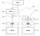
電子機器又は表示モジュールは2つの表示パネルを有し、一方の表示パネルに(すなわち、一方の表示パネルの表示領域の周辺部)、当該表示パネルの動作に必要な、若しくは当該表示パネルが組み込まれる電子機器に必要な回路を形成する。そして、当該表示パネルに組み込まれた回路によって、当該表示パネル、若しくは当該表示パネルが組み込まれる電子機器を駆動する。 An electronic device or a display module has two display panels, and one of the display panels (that is, the peripheral portion of the display area of one display panel) is necessary for the operation of the display panel or the display panel is incorporated. Circuits necessary for electronic equipment are formed. Then, the display panel or an electronic device in which the display panel is incorporated is driven by a circuit incorporated in the display panel.
本発明の液晶表示装置の一は、第1の液晶素子を含む第1の表示画面と、第1の端子を有する第1の表示パネルと、第2の液晶素子を含む第2の表示画面と、第2の端子と、回路群とを有する第2の表示パネルと、配線を有する基板とを有し、回路群は、第2の端子及び配線を介して第1の端子と電気的に接続されていることを特徴とする。 One aspect of the liquid crystal display device of the present invention includes a first display screen including a first liquid crystal element, a first display panel having a first terminal, and a second display screen including a second liquid crystal element. , A second display panel having a second terminal and a circuit group, and a substrate having wiring, and the circuit group is electrically connected to the first terminal through the second terminal and the wiring. It is characterized by being.
本発明の液晶表示装置の一は、第1の液晶素子を含む第1の表示画面と、第1の端子とを有する第1の表示パネルと、第2の液晶素子を含む第2の表示画面と、第2の端子と、回路群とを有する第2の表示パネルと、配線を有する基板と、集積回路とを有し、回路群は、第2の端子及び配線を介して第1の端子と電気的に接続され、集積回路は、配線を介して第2の端子と電気的に接続されていることを特徴とする。 One aspect of the liquid crystal display device of the present invention includes a first display screen including a first liquid crystal element, a first display panel having a first terminal, and a second display screen including a second liquid crystal element. And a second display panel having a second terminal and a circuit group, a substrate having wiring, and an integrated circuit. The circuit group includes the first terminal via the second terminal and the wiring. The integrated circuit is electrically connected to the second terminal through a wiring.
本発明の液晶表示装置の一は、第1の液晶素子を含む第1の表示画面と、第1の端子とを有する第1の表示パネルと、第2の液晶素子を含む第2の表示画面と、第2の端子と、回路群とを有する第2の表示パネルと、配線を有する基板と、センサとを有し、回路群は、第2の端子及び配線を介して第1の端子と電気的に接続され、センサは、配線を介して第2の端子と電気的に接続されていることを特徴とする。 One aspect of the liquid crystal display device of the present invention includes a first display screen including a first liquid crystal element, a first display panel having a first terminal, and a second display screen including a second liquid crystal element. And a second display panel having a second terminal and a circuit group, a substrate having wiring, and a sensor, and the circuit group includes the first terminal through the second terminal and the wiring. The sensor is electrically connected, and the sensor is electrically connected to the second terminal through a wiring.
本発明の液晶表示装置の一は、第1の液晶素子を含む第1の表示画面と、第1の端子とを有する第1の表示パネルと、第2の液晶素子を含む第2の表示画面と、第2の端子と、回路群とを有する第2の表示パネルと、配線を有する基板と、集積回路と、センサとを有し、回路群は、配線を介して第1の表示パネルと電気的に接続され、集積回路は、配線を介して第1の表示パネルと電気的に接続され、配線を介して第2の表示パネルと電気的に接続され、回路群は、第2の端子及び配線を介して第1の端子と電気的に接続され、集積回路は、配線を介して第2の端子と電気的に接続され、センサは、配線を介して第2の端子と電気的に接続されていることを特徴とする。 One aspect of the liquid crystal display device of the present invention includes a first display screen including a first liquid crystal element, a first display panel having a first terminal, and a second display screen including a second liquid crystal element. A second display panel having a second terminal and a circuit group, a substrate having wiring, an integrated circuit, and a sensor, and the circuit group includes a first display panel via the wiring. The integrated circuit is electrically connected to the first display panel through a wiring, and is electrically connected to the second display panel through the wiring. The circuit group is connected to the second terminal. And the first circuit is electrically connected to the first terminal through the wiring, the integrated circuit is electrically connected to the second terminal through the wiring, and the sensor is electrically connected to the second terminal through the wiring. It is connected.
本発明の液晶表示装置の一は、第1の液晶素子を含む第1の表示画面と、第1の端子、レベルシフタと、駆動回路とを有する第1の表示パネルと、第2の液晶素子を含む第2の表示画面と、第2の端子と、回路群とを有する第2の表示パネルと、配線を有する基板とを有し、回路群は、第2の端子及び配線を介して第1の端子と電気的に接続されていることを特徴とする。 According to one aspect of the liquid crystal display device of the present invention, a first display screen including a first liquid crystal element, a first display panel having a first terminal, a level shifter, and a driver circuit, and a second liquid crystal element are provided. A second display panel including a second display panel including a second terminal and a circuit group; and a substrate having a wiring. The circuit group includes a first terminal via the second terminal and the wiring. It is electrically connected to the terminal of.
本発明の液晶表示装置の一は、第1の液晶素子を含む第1の表示画面と、第1の端子、レベルシフタと、駆動回路とを有する第1の表示パネルと、第2の液晶素子を含む第2の表示画面と、第2の端子と、回路群とを有する第2の表示パネルと、配線を有する基板と、集積回路とを有し、回路群は、第2の端子及び配線を介して第1の端子と電気的に接続され、集積回路は、配線を介して第2の端子と電気的に接続されていることを特徴とする。 According to one aspect of the liquid crystal display device of the present invention, a first display screen including a first liquid crystal element, a first display panel having a first terminal, a level shifter, and a driver circuit, and a second liquid crystal element are provided. And a second display panel including a second display screen, a second terminal, and a circuit group, a substrate having wiring, and an integrated circuit. The circuit group includes the second terminal and the wiring. The integrated circuit is electrically connected to the second terminal through a wiring, and the integrated circuit is electrically connected to the second terminal through a wiring.
本発明の液晶表示装置の一は、第1の液晶素子を含む第1の表示画面と、第1の端子と、レベルシフタと、駆動回路とを有する第1の表示パネルと、第2の液晶素子を含む第2の表示画面と、第2の端子と、回路群とを有する第2の表示パネルと、配線を有する基板と、センサとを有し、回路群は、第2の端子及び配線を介して第1の端子と電気的に接続され、センサは、配線を介して第2の端子と電気的に接続されていることを特徴とする。 One aspect of the liquid crystal display device of the present invention includes a first display screen including a first liquid crystal element, a first terminal having a first terminal, a level shifter, and a drive circuit, and a second liquid crystal element. And a second display panel having a second terminal and a circuit group, a substrate having wiring, and a sensor. The circuit group includes the second terminal and wiring. The sensor is electrically connected to the first terminal via the wiring, and the sensor is electrically connected to the second terminal via the wiring.
本発明の液晶表示装置の一は、第1の液晶素子を含む第1の表示画面と、第1の端子と、レベルシフタと、駆動回路とを有する第1の表示パネルと、第2の液晶素子を含む第2の表示画面と、第2の端子と、回路群とを有する第2の表示パネルと、配線を有する基板と、集積回路と、センサとを有し、回路群は、配線を介して第1の表示パネルと電気的に接続され、集積回路は、配線を介して第1の表示パネルと電気的に接続され、回路群は、第2の端子及び配線を介して第1の端子と電気的に接続され、集積回路は、配線を介して第2の端子と電気的に接続され、センサは、配線を介して第2の端子と電気的に接続されていることを特徴とする。 One aspect of the liquid crystal display device of the present invention includes a first display screen including a first liquid crystal element, a first terminal having a first terminal, a level shifter, and a drive circuit, and a second liquid crystal element. And a second display panel having a second terminal and a circuit group, a substrate having wiring, an integrated circuit, and a sensor. The integrated circuit is electrically connected to the first display panel via a wiring, and the circuit group is connected to the first terminal via the second terminal and the wiring. The integrated circuit is electrically connected to the second terminal through a wiring, and the sensor is electrically connected to the second terminal through the wiring. .
なお、スイッチは、様々な形態のものを用いることができる。例としては、電気的スイッチや機械的なスイッチなどがある。つまり、電流の流れを制御できるものであればよく、特定のものに限定されない。例えば、スイッチとして、トランジスタ(例えば、バイポーラトランジスタ、MOSトランジスタなど)、ダイオード(例えば、PNダイオード、PINダイオード、ショットキーダイオード、MIM(Metal Insulator Metal)ダイオード、MIS(Metal Insulator Semiconductor)ダイオード、ダイオード接続のトランジスタなど)、サイリスタなどを用いることができる。または、これらを組み合わせた論理回路をスイッチとして用いることができる。 Note that various types of switches can be used. Examples include electrical switches and mechanical switches. That is, it is only necessary to be able to control the current flow, and is not limited to a specific one. For example, as a switch, a transistor (for example, bipolar transistor, MOS transistor, etc.), a diode (for example, PN diode, PIN diode, Schottky diode, MIM (Metal Insulator Metal) diode, MIS (Metal Insulator Semiconductor) diode, diode-connected Transistor), a thyristor, or the like can be used. Alternatively, a logic circuit combining these can be used as a switch.
スイッチとしてトランジスタを用いる場合、そのトランジスタは、単なるスイッチとして動作するため、トランジスタの極性(導電型)は特に限定されない。ただし、オフ電流を抑えたい場合、オフ電流が少ない方の極性のトランジスタを用いることが望ましい。オフ電流が少ないトランジスタとしては、LDD領域を有するトランジスタやマルチゲート構造を有するトランジスタ等がある。または、スイッチとして動作させるトランジスタのソース端子の電位が、低電位側電源(Vss、GND、0Vなど)の電位に近い状態で動作する場合はNチャネル型トランジスタを用いることが望ましい。反対に、ソース端子の電位が、高電位側電源(Vddなど)の電位に近い状態で動作する場合はPチャネル型トランジスタを用いることが望ましい。なぜなら、Nチャネル型トランジスタではソース端子が低電位側電源の電位に近い状態で動作するとき、Pチャネル型トランジスタではソース端子が高電位側電源の電位に近い状態で動作するとき、ゲートとソースの間の電圧の絶対値を大きくできるため、スイッチとして、動作をさせやすいからである。ソースフォロワ動作をしてしまうことが少ないため、出力電圧の大きさが小さくなってしまうことが少ないからである。 In the case where a transistor is used as a switch, the transistor operates as a mere switch, and thus the polarity (conductivity type) of the transistor is not particularly limited. However, when it is desired to suppress off-state current, it is desirable to use a transistor having a polarity with smaller off-state current. As a transistor with low off-state current, a transistor having an LDD region, a transistor having a multi-gate structure, and the like can be given. Alternatively, an N-channel transistor is preferably used in the case where the transistor operates as a switch when the potential of the source terminal of the transistor is close to the potential of the low potential power supply (Vss, GND, 0 V, or the like). On the other hand, it is desirable to use a P-channel transistor when operating in a state where the potential of the source terminal is close to the potential of the high potential side power supply (Vdd or the like). This is because an N-channel transistor operates when the source terminal is close to the potential of the low-potential side power supply, and a P-channel transistor operates when the source terminal is close to the potential of the high-potential side power supply. This is because the absolute value of the voltage between them can be increased, and it is easy to operate as a switch. This is because the source follower operation is rare and the output voltage is less likely to decrease.
なお、Nチャネル型トランジスタとPチャネル型トランジスタの両方を用いて、CMOS型のスイッチをスイッチとして用いてもよい。CMOS型のスイッチにすると、Pチャネル型トランジスタまたはNチャネル型トランジスタのどちらか一方のトランジスタが導通すれば電流が流れるため、スイッチとして機能しやすくなる。例えば、スイッチへの入力信号の電圧が高い場合でも、低い場合でも、適切に電圧を出力させることができる。さらに、スイッチをオンまたはオフさせるための信号の電圧振幅値を小さくすることができるので、消費電力を小さくすることもできる。 Note that a CMOS switch may be used as a switch by using both an N-channel transistor and a P-channel transistor. When a CMOS switch is used, a current flows when one of the P-channel transistor and the N-channel transistor is turned on, so that the switch can easily function as a switch. For example, the voltage can be appropriately output regardless of whether the voltage of the input signal to the switch is high or low. Further, since the voltage amplitude value of the signal for turning on or off the switch can be reduced, the power consumption can be reduced.
なお、スイッチとしてトランジスタを用いる場合、スイッチは、入力端子(ソース端子またはドレイン端子の一方)と、出力端子(ソース端子またはドレイン端子の他方)と、導通を制御する端子(ゲート端子)とを有している。一方、スイッチとしてダイオードを用いる場合、スイッチは、導通を制御する端子を有していない場合がある。そのため、トランジスタよりもダイオードをスイッチとして用いた方が、端子を制御するための配線を少なくすることができる。 Note that when a transistor is used as a switch, the switch has an input terminal (one of a source terminal or a drain terminal), an output terminal (the other of the source terminal or the drain terminal), and a terminal for controlling conduction (a gate terminal). is doing. On the other hand, when a diode is used as the switch, the switch may not have a terminal for controlling conduction. Therefore, the use of a diode as a switch rather than a transistor can reduce the wiring for controlling the terminal.
なお、AとBとが接続されている、と明示的に記載する場合は、AとBとが電気的に接続されている場合と、AとBとが機能的に接続されている場合と、AとBとが直接接続されている場合とを含むものとする。ここで、A、Bは、対象物(例えば、装置、素子、回路、配線、電極、端子、導電膜、層、など)であるとする。したがって、所定の接続関係、例えば、図または文章に示された接続関係に限定されず、図または文章に示された接続関係以外のものも含むものとする。 In addition, when it is explicitly described that A and B are connected, A and B are electrically connected, and A and B are functionally connected. , A and B are directly connected. Here, A and B are objects (for example, devices, elements, circuits, wirings, electrodes, terminals, conductive films, layers, etc.). Therefore, it is not limited to a predetermined connection relationship, for example, the connection relationship shown in the figure or text, and includes things other than the connection relation shown in the figure or text.
例えば、AとBとが電気的に接続されている場合として、AとBとの電気的な接続を可能とする素子(例えば、スイッチ、トランジスタ、容量素子、インダクタ、抵抗素子、ダイオードなど)が、AとBとの間に1個以上配置されていてもよい。あるいは、AとBとが機能的に接続されている場合として、AとBとの機能的な接続を可能とする回路(例えば、論理回路(インバータ、NAND回路、NOR回路など)、信号変換回路(DA変換回路、AD変換回路、ガンマ補正回路など)、電位レベル変換回路(電源回路(昇圧回路、降圧回路など)、信号の電位レベルを変えるレベルシフタ回路など)、電圧源、電流源、切り替え回路、増幅回路(信号振幅または電流量などを大きくできる回路、オペアンプ、差動増幅回路、ソースフォロワ回路、バッファ回路など)、信号生成回路、記憶回路、制御回路など)が、AとBとの間に1個以上配置されていてもよい。あるいは、AとBとが直接接続されている場合として、AとBとの間に他の素子や他の回路を挟まずに、AとBとが直接接続されていてもよい。 For example, when A and B are electrically connected, an element (for example, a switch, a transistor, a capacitor, an inductor, a resistance element, a diode, or the like) that enables electrical connection between A and B is provided. 1 or more may be arranged between A and B. Alternatively, when A and B are functionally connected, a circuit (for example, a logic circuit (an inverter, a NAND circuit, a NOR circuit, etc.), a signal conversion circuit that enables functional connection between A and B (DA conversion circuit, AD conversion circuit, gamma correction circuit, etc.), potential level conversion circuit (power supply circuit (boost circuit, step-down circuit, etc.), level shifter circuit that changes signal potential level), voltage source, current source, switching circuit , Amplifier circuits (circuits that can increase signal amplitude or current amount, operational amplifiers, differential amplifier circuits, source follower circuits, buffer circuits, etc.), signal generation circuits, memory circuits, control circuits, etc.) between A and B One or more of them may be arranged. Alternatively, when A and B are directly connected, A and B may be directly connected without sandwiching other elements or other circuits between A and B.
なお、AとBとが直接接続されている、と明示的に記載する場合は、AとBとが直接接続されている場合(つまり、AとBとの間に他の素子や他の回路を間に介さずに接続されている場合)と、AとBとが電気的に接続されている場合(つまり、AとBとの間に別の素子や別の回路を挟んで接続されている場合)とを含むものとする。 Note that in the case where it is explicitly described that A and B are directly connected, when A and B are directly connected (that is, another element or other circuit between A and B). ) And A and B are electrically connected (that is, A and B are connected with another element or another circuit sandwiched between them). ).
なお、AとBとが電気的に接続されている、と明示的に記載する場合は、AとBとが電気的に接続されている場合(つまり、AとBとの間に別の素子や別の回路を挟んで接続されている場合)と、AとBとが機能的に接続されている場合(つまり、AとBとの間に別の回路を挟んで機能的に接続されている場合)と、AとBとが直接接続されている場合(つまり、AとBとの間に別の素子や別の回路を挟まずに接続されている場合)とを含むものとする。つまり、電気的に接続されている、と明示的に記載する場合は、単に、接続されている、とのみ明示的に記載されている場合と同じであるとする。 Note that in the case where it is explicitly described that A and B are electrically connected, another element is connected between A and B (that is, between A and B). Or when A and B are functionally connected (that is, they are functionally connected with another circuit between A and B). And a case where A and B are directly connected (that is, a case where another element or another circuit is not connected between A and B). That is, when it is explicitly described that it is electrically connected, it is the same as when it is explicitly only described that it is connected.
なお、表示素子、表示素子を有する装置である表示装置、発光素子、発光素子を有する装置である発光装置は、様々な形態を用いたり、様々な素子を有することができる。例えば、表示素子、表示装置、発光素子または発光装置としては、EL素子(有機物及び無機物を含むEL素子、有機EL素子、無機EL素子)、電子放出素子、液晶素子、電子インク、電気泳動素子、グレーティングライトバルブ(GLV)、プラズマディスプレイ(PDP)、デジタルマイクロミラーデバイス(DMD)、圧電セラミックディスプレイ、カーボンナノチューブ、など、電気磁気的作用により、コントラスト、輝度、反射率、透過率などが変化する表示媒体を用いることができる。なお、EL素子を用いた表示装置としてはELディスプレイ、電子放出素子を用いた表示装置としてはフィールドエミッションディスプレイ(FED)やSED方式平面型ディスプレイ(SED:Surface−conduction Electron−emitter Disply)など、液晶素子を用いた表示装置としては液晶ディスプレイ(透過型液晶ディスプレイ、半透過型液晶ディスプレイ、反射型液晶ディスプレイ、直視型液晶ディスプレイ、投射型液晶ディスプレイ)、電子インクや電気泳動素子を用いた表示装置としては電子ペーパーがある。 Note that a display element, a display device that includes a display element, a light-emitting element, and a light-emitting device that includes a light-emitting element can have various modes or have various elements. For example, as a display element, a display device, a light-emitting element, or a light-emitting device, an EL element (an EL element including an organic substance and an inorganic substance, an organic EL element, an inorganic EL element), an electron-emitting element, a liquid crystal element, electronic ink, an electrophoretic element, Grating light valve (GLV), plasma display (PDP), digital micromirror device (DMD), piezoelectric ceramic display, carbon nanotube, and other displays that change contrast, brightness, reflectivity, transmittance, etc. due to electromagnetic action Media can be used. Note that a display device using an EL element is an EL display, and a display device using an electron-emitting device is a liquid crystal display such as a field emission display (FED) or a SED type flat display (SED: Surface-conduction Electron-Emitter Display). Liquid crystal displays (transmission type liquid crystal display, transflective type liquid crystal display, reflection type liquid crystal display, direct view type liquid crystal display, projection type liquid crystal display), display devices using electronic ink and electrophoretic elements There is electronic paper.
なお、EL素子とは、陽極と、陰極と、陽極と陰極との間に挟まれたEL層とを有する素子である。なお、EL層としては、1重項励起子からの発光(蛍光)を利用するもの、3重項励起子からの発光(燐光)を利用するもの、1重項励起子からの発光(蛍光)を利用するものと3重項励起子からの発光(燐光)を利用するものとを含むもの、有機物によって形成されたもの、無機物によって形成されたもの、有機物によって形成されたものと無機物によって形成されたものとを含むもの、高分子の材料、低分子の材料、高分子の材料と低分子の材料とを含むものなどを用いることができる。ただし、これに限定されず、EL素子として様々なものを用いることができる。 Note that an EL element is an element having an anode, a cathode, and an EL layer sandwiched between the anode and the cathode. Note that the EL layer uses light emission from singlet excitons (fluorescence), uses light emission from triplet excitons (phosphorescence), and emits light from singlet excitons (fluorescence). And those using triplet excitons (phosphorescence), those made of organic matter, those made of inorganic matter, those made of organic matter and those made of inorganic matter And a high molecular weight material, a low molecular weight material, a high molecular weight material and a low molecular weight material, or the like can be used. However, the present invention is not limited to this, and various EL elements can be used.
なお、電子放出素子とは、先鋭な陰極に高電界を集中して電子を引き出す素子である。例えば、電子放出素子として、スピント型、カーボンナノチューブ(CNT)型、金属―絶縁体―金属を積層したMIM(Metal−Insulator−Metal)型、金属―絶縁体―半導体を積層したMIS(Metal−Insulator−Semiconductor)型、MOS型、シリコン型、薄膜ダイオード型、ダイヤモンド型、表面伝導エミッタSCD型、金属―絶縁体―半導体−金属型等の薄膜型、HEED型、EL型、ポーラスシリコン型、表面伝導(SED)型などを用いることができる。ただし、これに限定されず、電子放出素子として様々なものを用いることができる。 The electron-emitting device is an element that draws electrons by concentrating a high electric field on a sharp cathode. For example, as an electron-emitting device, a Spindt type, a carbon nanotube (CNT) type, a metal-insulator-metal laminated MIM (Metal-Insulator-Metal) type, and a metal-insulator-semiconductor laminated MIS (Metal-Insulator). -Semiconductor) type, MOS type, silicon type, thin film diode type, diamond type, surface conduction emitter SCD type, metal-insulator-semiconductor-metal thin film type, HEED type, EL type, porous silicon type, surface conduction (SED) type etc. can be used. However, the present invention is not limited to this, and various types of electron-emitting devices can be used.
なお、液晶素子とは、液晶の光学的変調作用によって光の透過または非透過を制御する素子であり、一対の電極、及び液晶により構成される。なお、液晶の光学的変調作用は、液晶にかかる電界(横方向の電界、縦方向の電界又は斜め方向の電界を含む)によって制御される。なお、液晶素子としては、ネマチック液晶、コレステリック液晶、スメクチック液晶、ディスコチック液晶、サーモトロピック液晶、リオトロピック液晶、低分子液晶、高分子液晶、強誘電液晶、反強誘電液晶、主鎖型液晶、側鎖型高分子液晶、プラズマアドレス液晶(PALC)、バナナ型液晶などが挙げられる。また、液晶の軌道方式としては、TN(Twisted Nematic)モード、STN(Super Twisted Nematic)モード、IPS(In−Plane−Switching)モード、FFS(Fringe Field Switching)モード、MVA(Multi−domain Vertical Alignment)モード、PVA(Patterned Vertical Alignment)モード、ASV(Advanced Super View)モード、ASM(Axially Symmetric aligned Micro−cell)モード、OCB(Optical Compensated Birefringence)モード、ECB(Electrically Controlled Birefringence)モード、FLC(Ferroelectric Liquid Crystal)モード、AFLC(AntiFerroelectric Liquid Crystal)モード、PDLC(Polymer Dispersed Liquid Crystal)モード、ゲストホストモードなどを用いることができる。ただし、これに限定されず、液晶素子及びその駆動方式として様々なものを用いることができる。 Note that a liquid crystal element is an element that controls transmission or non-transmission of light by an optical modulation action of liquid crystal and includes a pair of electrodes and liquid crystal. Note that the optical modulation action of the liquid crystal is controlled by an electric field applied to the liquid crystal (including a horizontal electric field, a vertical electric field, or an oblique electric field). Liquid crystal elements include nematic liquid crystal, cholesteric liquid crystal, smectic liquid crystal, discotic liquid crystal, thermotropic liquid crystal, lyotropic liquid crystal, low molecular liquid crystal, polymer liquid crystal, ferroelectric liquid crystal, antiferroelectric liquid crystal, main chain liquid crystal, side Examples include chain polymer liquid crystals, plasma addressed liquid crystals (PALC), and banana liquid crystals. In addition, as the liquid crystal orbital method, a TN (Twisted Nematic) mode, an STN (Super Twisted Nematic) mode, an IPS (In-Plane-Switching) mode, an FFS (Fringe Field Switching) mode, and an MVA (Multi-Antificant Magnetic Magnetic Delta) mode are used. Mode, PVA (Patterned Vertical Alignment) mode, ASV (Advanced Super View) mode, ASM (Axially Symmetrical Micro-cell) mode, OCB (Optical Compensated BEC) Rolled Birefringence (FLC) mode, FLC (Ferroelectric Liquid Crystal) mode, AFLC (Anti-Ferroelectric Liquid Crystal) mode, PDLC (Polymer Dispersed Liquid Crystal) mode, guest host mode, etc. However, the present invention is not limited to this, and various liquid crystal elements and driving methods thereof can be used.
なお、電子ペーパーとしては、光学異方性と染料分子配向のような分子により表示されるもの、電気泳動、粒子移動、粒子回転、相変化のような粒子により表示されるもの、フィルムの一端が移動することにより表示されるもの、分子の発色/相変化により表示されるもの、分子の光吸収により表示されるもの、電子とホールが結合して自発光により表示されるものなどのことをいう。例えば、電子ペーパーとして、マイクロカプセル型電気泳動、水平移動型電気泳動、垂直移動型電気泳動、球状ツイストボール、磁気ツイストボール、円柱ツイストボール方式、帯電トナー、電子粉流体、磁気泳動型、磁気感熱式、エレクトロウェッテイング、光散乱(透明/白濁変化)、コレステリック液晶/光導電層、コレステリック液晶、双安定性ネマチック液晶、強誘電性液晶、2色性色素・液晶分散型、可動フィルム、ロイコ染料による発消色、フォトクロミック、エレクトロクロミック、エレクトロデポジション、フレキシブル有機ELなどを用いることができる。ただし、これに限定されず、電子ペーパーとして様々なものを用いることができる。ここで、マイクロカプセル型電気泳動を用いることによって、電気泳動方式の欠点である泳動粒子の凝集、沈殿を解決することができる。電子粉流体は、高速応答性、高反射率、広視野角、低消費電力、メモリー性などのメリットを有する。 Electronic paper includes those displayed by molecules such as optical anisotropy and dye molecule orientation, those displayed by particles such as electrophoresis, particle movement, particle rotation, and phase change. It is displayed by moving, displayed by color development / phase change of molecules, displayed by light absorption of molecules, displayed by self-emission by combining electrons and holes, etc. . For example, as electronic paper, microcapsule type electrophoresis, horizontal movement type electrophoresis, vertical movement type electrophoresis, spherical twist ball, magnetic twist ball, cylindrical twist ball method, charged toner, electronic powder fluid, magnetophoretic type, magnetic heat sensitivity Formula, electrowetting, light scattering (transparency / translucency change), cholesteric liquid crystal / photoconductive layer, cholesteric liquid crystal, bistable nematic liquid crystal, ferroelectric liquid crystal, dichroic dye / liquid crystal dispersion type, movable film, leuco dye Coloring / decoloring by photo, photochromic, electrochromic, electrodeposition, flexible organic EL, etc. can be used. However, the present invention is not limited to this, and various electronic papers can be used. Here, by using microcapsule electrophoresis, aggregation and precipitation of electrophoretic particles, which is a drawback of the electrophoresis system, can be solved. The electronic powder fluid has advantages such as high-speed response, high reflectivity, wide viewing angle, low power consumption, and memory properties.
なお、プラズマディスプレイパネルは、電極を表面に形成した基板と、電極及び微小な溝を表面に形成し且つ溝内に蛍光体層を形成した基板とを狭い間隔で対向させて、希ガスを封入した構造を有する。なお、電極間に電圧をかけることによって紫外線を発生させ、蛍光体を光らせることで、表示を行うことができる。なお、プラズマディスプレイパネルとしては、DC型PDP、AC型PDPでもよい。ここで、プラズマディスプレイパネルとしては、AWS(Address While Sustain)駆動、サブフレームをリセット期間、アドレス期間、維持期間に分割するADS(Address Display Separated)駆動、CLEAR(High Contrast, Low Energy Address and Reduction of False Contour Sequence)駆動、ALIS(Alternate Lighting of Surfaces)方式、TERES(Technology of Reciprocal Sustainer)駆動などを用いることができる。ただし、これに限定されず、プラズマディスプレイパネルとして様々なものを用いることができる。 Note that the plasma display panel encloses a rare gas with a substrate having electrodes formed on the surface thereof and a substrate having electrodes and minute grooves formed on the surface and having a phosphor layer formed in the grooves facing each other at a narrow interval. Has the structure. In addition, a display can be performed by generating an ultraviolet-ray by applying a voltage between electrodes and making fluorescent substance light. The plasma display panel may be a DC type PDP or an AC type PDP. Here, the plasma display panel includes AWS (Address Wide Sustain) drive, ADS (Address Display Separated) drive that divides the subframe into a reset period, an address period, and a sustain period, and CLEAR (High Contrast Address, Low Energy Address). False control sequence (ALIS) drive, ALIS (Alternate Lighting of Surfaces) system, TERES (Technology of Reciprocal Sustainer) drive, or the like can be used. However, the present invention is not limited to this, and various types of plasma display panels can be used.
なお、光源を必要とする表示装置、例えば、液晶ディスプレイ(透過型液晶ディスプレイ、半透過型液晶ディスプレイ、反射型液晶ディスプレイ、直視型液晶ディスプレイ、投射型液晶ディスプレイ)、グレーティングライトバルブ(GLV)を用いた表示装置、デジタルマイクロミラーデバイス(DMD)を用いた表示装置などの光源としては、エレクトロルミネッセンス、冷陰極管、熱陰極管、LED、レーザー光源、水銀ランプなどを用いることができる。ただし、これに限定されず、光源して様々なものを用いることができる。 Note that a display device that requires a light source, such as a liquid crystal display (transmission type liquid crystal display, transflective type liquid crystal display, reflection type liquid crystal display, direct view type liquid crystal display, projection type liquid crystal display), or a grating light valve (GLV) is used. As a light source for a display device using a conventional display device or a digital micromirror device (DMD), electroluminescence, a cold cathode tube, a hot cathode tube, an LED, a laser light source, a mercury lamp, or the like can be used. However, the present invention is not limited to this, and various light sources can be used.
なお、トランジスタとして、様々な形態のトランジスタを用いることができる。よって、用いるトランジスタの種類に限定はない。例えば、非晶質シリコン、多結晶シリコン、微結晶(マイクロクリスタル、セミアモルファスとも言う)シリコンなどに代表される非単結晶半導体膜を有する薄膜トランジスタ(TFT)などを用いることができる。TFTを用いる場合、様々なメリットがある。例えば、単結晶シリコンの場合よりも低い温度で製造できるため、製造コストの削減、又は製造装置の大型化を図ることができる。製造装置を大きくできるため、大型基板上に製造できる。そのため、同時に多くの個数の表示装置を製造できるため、低コストで製造できる。さらに、製造温度が低いため、耐熱性の弱い基板を用いることができる。そのため、透明基板上にトランジスタを製造できる。そして、透明な基板上のトランジスタを用いて表示素子での光の透過を制御することができる。あるいは、トランジスタの膜厚が薄いため、トランジスタを構成する膜の一部は、光を透過させることができる。そのため、開口率が向上させることができる。 Note that various types of transistors can be used as the transistor. Thus, there is no limitation on the type of transistor used. For example, a thin film transistor (TFT) including a non-single-crystal semiconductor film typified by amorphous silicon, polycrystalline silicon, microcrystalline (also referred to as semi-amorphous) silicon, or the like can be used. When using TFT, there are various advantages. For example, since manufacturing can be performed at a lower temperature than that of single crystal silicon, manufacturing cost can be reduced or a manufacturing apparatus can be increased in size. Since the manufacturing apparatus can be enlarged, it can be manufactured on a large substrate. Therefore, since a large number of display devices can be manufactured at the same time, it can be manufactured at low cost. Furthermore, since the manufacturing temperature is low, a substrate with low heat resistance can be used. Therefore, a transistor can be manufactured on a transparent substrate. Then, light transmission through the display element can be controlled using a transistor over a transparent substrate. Alternatively, since the thickness of the transistor is small, part of the film included in the transistor can transmit light. Therefore, the aperture ratio can be improved.
なお、多結晶シリコンを製造するときに、触媒(ニッケルなど)を用いることにより、結晶性をさらに向上させ、電気特性のよいトランジスタを製造することが可能となる。その結果、ゲートドライバ回路(走査線駆動回路)やソースドライバ回路(信号線駆動回路)、信号処理回路(信号生成回路、ガンマ補正回路、DA変換回路など)を基板上に一体形成することができる。 Note that by using a catalyst (such as nickel) when manufacturing polycrystalline silicon, it is possible to further improve crystallinity and to manufacture a transistor with favorable electrical characteristics. As a result, a gate driver circuit (scanning line driving circuit), a source driver circuit (signal line driving circuit), and a signal processing circuit (signal generation circuit, gamma correction circuit, DA conversion circuit, etc.) can be integrally formed on the substrate. .
なお、微結晶シリコンを製造するときに、触媒(ニッケルなど)を用いることにより、結晶性をさらに向上させ、電気特性のよいトランジスタを製造することが可能となる。このとき、レーザー照射を行うことなく、熱処理を加えるだけで、結晶性を向上させることができる。その結果、ゲートドライバ回路(走査線駆動回路)やソースドライバ回路の一部(アナログスイッチなど)を基板上に一体形成することができる。さらに、結晶化のためにレーザー照射を行わない場合は、シリコンの結晶性のムラを抑えることができる。そのため、綺麗な画像を表示することができる。 Note that when a microcrystalline silicon is manufactured, by using a catalyst (such as nickel), crystallinity can be further improved and a transistor with favorable electrical characteristics can be manufactured. At this time, crystallinity can be improved only by applying heat treatment without laser irradiation. As a result, part of the gate driver circuit (scanning line driving circuit) and the source driver circuit (such as an analog switch) can be formed over the substrate. Furthermore, in the case where laser irradiation is not performed for crystallization, the crystallinity unevenness of silicon can be suppressed. Therefore, a beautiful image can be displayed.
ただし、触媒(ニッケルなど)を用いずに、多結晶シリコンや微結晶シリコンを製造することは可能である。 However, it is possible to produce polycrystalline silicon or microcrystalline silicon without using a catalyst (such as nickel).
なお、シリコンの結晶性を、多結晶または微結晶などへと向上させることは、パネル全体で行うことが望ましいが、それに限定されない。パネルの一部の領域のみにおいて、シリコンの結晶性を向上させてもよい。選択的に結晶性を向上させることは、レーザー光を選択的に照射することなどにより可能である。例えば、画素以外の領域である周辺回路領域にのみ、レーザー光を照射してもよい。または、ゲートドライバ回路、ソースドライバ回路等の領域にのみ、レーザー光を照射してもよい。あるいは、ソースドライバ回路の一部(例えば、アナログスイッチ)の領域にのみ、レーザー光を照射してもよい。その結果、回路を高速に動作させる必要がある領域にのみ、シリコンの結晶化を向上させることができる。画素領域は、高速に動作させる必要性が低いため、結晶性が向上されなくても、問題なく画素回路を動作させることができる。結晶性を向上させる領域が少なくて済むため、製造工程も短くすることができ、スループットが向上し、製造コストを低減させることができる。必要とされる製造装置の数も少なくて製造できるため、製造コストを低減させることができる。 Note that it is preferable to improve the crystallinity of silicon to be polycrystalline or microcrystalline, but the present invention is not limited to this. The crystallinity of silicon may be improved only in a partial region of the panel. The crystallinity can be selectively improved by selectively irradiating laser light. For example, the laser beam may be irradiated only to the peripheral circuit region that is a region other than the pixel. Alternatively, the laser beam may be irradiated only on a region such as a gate driver circuit or a source driver circuit. Or you may irradiate a laser beam only to the area | region (for example, analog switch) of a source driver circuit. As a result, crystallization of silicon can be improved only in a region where the circuit needs to operate at high speed. Since it is not necessary to operate the pixel region at high speed, the pixel circuit can be operated without any problem even if the crystallinity is not improved. Since the number of regions for improving crystallinity is small, the manufacturing process can be shortened, the throughput can be improved, and the manufacturing cost can be reduced. Since the number of manufacturing apparatuses required is small, the manufacturing cost can be reduced.
または、半導体基板やSOI基板などを用いてトランジスタを形成することができる。これらにより、特性やサイズや形状などのバラツキが少なく、電流供給能力が高く、サイズの小さいトランジスタを製造することができる。これらのトランジスタを用いると、回路の低消費電力化、又は回路の高集積化を図ることができる。 Alternatively, a transistor can be formed using a semiconductor substrate, an SOI substrate, or the like. Accordingly, a transistor with small variations in characteristics, size, shape, and the like, high current supply capability, and small size can be manufactured. When these transistors are used, low power consumption of the circuit or high integration of the circuit can be achieved.
または、ZnO、a−InGaZnO、SiGe、GaAs、IZO、ITO、SnOなどの化合物半導体または酸化物半導体を有するトランジスタや、さらに、これらの化合物半導体または酸化物半導体を薄膜化した薄膜トランジスタなどを用いることができる。これらにより、製造温度を低くでき、例えば、室温でトランジスタを製造することが可能となる。その結果、耐熱性の低い基板、例えばプラスチック基板やフィルム基板に直接トランジスタを形成することができる。なお、これらの化合物半導体または酸化物半導体を、トランジスタのチャネル部分に用いるだけでなく、それ以外の用途で用いることもできる。例えば、これらの化合物半導体または酸化物半導体を抵抗素子、画素電極、透明電極として用いることができる。さらに、それらをトランジスタと同時に成膜又は形成できるため、コストを低減できる。 Alternatively, a transistor having a compound semiconductor or an oxide semiconductor such as ZnO, a-InGaZnO, SiGe, GaAs, IZO, ITO, or SnO, or a thin film transistor in which these compound semiconductor or oxide semiconductor is thinned can be used. it can. Accordingly, the manufacturing temperature can be lowered, and for example, the transistor can be manufactured at room temperature. As a result, the transistor can be formed directly on a substrate having low heat resistance, such as a plastic substrate or a film substrate. Note that these compound semiconductors or oxide semiconductors can be used not only for a channel portion of a transistor but also for other purposes. For example, these compound semiconductors or oxide semiconductors can be used as resistance elements, pixel electrodes, and transparent electrodes. Furthermore, since these can be formed or formed simultaneously with the transistor, cost can be reduced.
または、インクジェットや印刷法を用いて形成したトランジスタなどを用いることができる。これらにより、室温で製造、低真空度で製造、又は大型基板上に製造することができる。マスク(レチクル)を用いなくても製造することが可能となるため、トランジスタのレイアウトを容易に変更することができる。さらに、レジストを用いる必要がないので、材料費が安くなり、工程数を削減できる。さらに、必要な部分にのみ膜を付けるため、全面に成膜した後でエッチングする、という製法よりも、材料が無駄にならず、低コストにできる。 Alternatively, a transistor formed using an inkjet method or a printing method can be used. By these, it can manufacture at room temperature, manufacture at a low vacuum degree, or can manufacture on a large sized board | substrate. Since the transistor can be manufactured without using a mask (reticle), the layout of the transistor can be easily changed. Furthermore, since it is not necessary to use a resist, the material cost is reduced and the number of processes can be reduced. Further, since a film is formed only on a necessary portion, the material is not wasted and cost can be reduced as compared with a manufacturing method in which etching is performed after film formation on the entire surface.
または、有機半導体やカーボンナノチューブを有するトランジスタ等を用いることができる。これらにより、曲げることが可能な基板上にトランジスタを形成することができる。そのため、有機半導体やカーボンナノチューブを有するトランジスタなどを用いた装置は衝撃に強くできる。 Alternatively, a transistor including an organic semiconductor or a carbon nanotube can be used. Thus, a transistor can be formed over a substrate that can be bent. Therefore, an apparatus using an organic semiconductor or a transistor having a carbon nanotube can be resistant to impact.
さらに、様々な構造のトランジスタを用いることができる。例えば、MOS型トランジスタ、接合型トランジスタ、バイポーラトランジスタなどをトランジスタとして用いることができる。MOS型トランジスタを用いることにより、トランジスタのサイズを小さくすることができる。よって、多数のトランジスタを搭載することができる。バイポーラトランジスタを用いることにより、大きな電流を流すことができる。よって、高速に回路を動作させることができる。 In addition, transistors with various structures can be used. For example, a MOS transistor, a junction transistor, a bipolar transistor, or the like can be used as the transistor. By using a MOS transistor, the size of the transistor can be reduced. Therefore, a large number of transistors can be mounted. By using a bipolar transistor, a large current can flow. Therefore, the circuit can be operated at high speed.
なお、MOS型トランジスタ、バイポーラトランジスタなどを1つの基板に混在させて形成してもよい。これにより、低消費電力、小型化、高速動作などを実現することができる。 Note that a MOS transistor, a bipolar transistor, or the like may be formed over one substrate. Thereby, low power consumption, miniaturization, high-speed operation, etc. can be realized.
その他、様々なトランジスタを用いることができる。 In addition, various transistors can be used.
なお、トランジスタは、様々な基板を用いて形成することができる。基板の種類は、特定のものに限定されることはない。その基板としては、例えば、単結晶基板、SOI基板、ガラス基板、石英基板、プラスチック基板、紙基板、セロファン基板、石材基板、木材基板、布基板(天然繊維(絹、綿、麻)、合成繊維(ナイロン、ポリウレタン、ポリエステル)若しくは再生繊維(アセテート、キュプラ、レーヨン、再生ポリエステル)などを含む)、皮革基板、ゴム基板、ステンレス・スチル基板、ステンレス・スチル・ホイルを有する基板などを用いることができる。あるいは、人などの動物の皮膚(表皮、真皮)又は皮下組織を基板として用いてもよい。または、ある基板を用いてトランジスタを形成し、その後、別の基板にトランジスタを転置してもよい。トランジスタが転置される基板としては、単結晶基板、SOI基板、ガラス基板、石英基板、プラスチック基板、紙基板、セロファン基板、石材基板、木材基板、布基板(天然繊維(絹、綿、麻)、合成繊維(ナイロン、ポリウレタン、ポリエステル)若しくは再生繊維(アセテート、キュプラ、レーヨン、再生ポリエステル)などを含む)、皮革基板、ゴム基板、ステンレス・スチル基板、ステンレス・スチル・ホイルを有する基板などを用いることができる。あるいは、人などの動物の皮膚(表皮、真皮)又は皮下組織をトランジスタが転置される基板として用いてもよい。または、ある基板を用いてトランジスタを形成し、その基板を研磨して薄くしてもよい。研磨される基板としては、単結晶基板、SOI基板、ガラス基板、石英基板、プラスチック基板、紙基板、セロファン基板、石材基板、木材基板、布基板(天然繊維(絹、綿、麻)、合成繊維(ナイロン、ポリウレタン、ポリエステル)若しくは再生繊維(アセテート、キュプラ、レーヨン、再生ポリエステル)などを含む)、皮革基板、ゴム基板、ステンレス・スチル基板、ステンレス・スチル・ホイルを有する基板などを用いることができる。あるいは、人などの動物の皮膚(表皮、真皮)又は皮下組織を研磨される基板として用いてもよい。これらの基板を用いることにより、特性のよいトランジスタの形成、消費電力の小さいトランジスタの形成、壊れにくい装置の製造、耐熱性の付与、軽量化、又は薄型化を図ることができる。 Note that the transistor can be formed using various substrates. The kind of board | substrate is not limited to a specific thing. As the substrate, for example, single crystal substrate, SOI substrate, glass substrate, quartz substrate, plastic substrate, paper substrate, cellophane substrate, stone substrate, wood substrate, cloth substrate (natural fiber (silk, cotton, hemp), synthetic fiber) (Including nylon, polyurethane, polyester) or recycled fibers (including acetate, cupra, rayon, recycled polyester), leather substrates, rubber substrates, stainless steel substrates, substrates with stainless steel foils, etc. can be used. . Alternatively, the skin (epidermis, dermis) or subcutaneous tissue of an animal such as a human may be used as the substrate. Alternatively, a transistor may be formed using a certain substrate, and then the transistor may be transferred to another substrate. As a substrate to which the transistor is transferred, a single crystal substrate, an SOI substrate, a glass substrate, a quartz substrate, a plastic substrate, a paper substrate, a cellophane substrate, a stone substrate, a wood substrate, a cloth substrate (natural fiber (silk, cotton, hemp), Use synthetic fibers (nylon, polyurethane, polyester) or recycled fibers (including acetate, cupra, rayon, recycled polyester), leather substrates, rubber substrates, stainless steel substrates, substrates with stainless steel foil, etc. Can do. Alternatively, skin (epidermis, dermis) or subcutaneous tissue of an animal such as a human may be used as a substrate to which a transistor is transferred. Alternatively, a transistor may be formed using a certain substrate, and the substrate may be polished and thinned. As substrates to be polished, single crystal substrates, SOI substrates, glass substrates, quartz substrates, plastic substrates, paper substrates, cellophane substrates, stone substrates, wood substrates, cloth substrates (natural fibers (silk, cotton, hemp), synthetic fibers) (Including nylon, polyurethane, polyester) or recycled fibers (including acetate, cupra, rayon, recycled polyester), leather substrates, rubber substrates, stainless steel substrates, substrates with stainless steel foils, etc. can be used. . Alternatively, the skin (epidermis, dermis) or subcutaneous tissue of an animal such as a human may be used as a substrate to be polished. By using these substrates, it is possible to form a transistor with good characteristics, a transistor with low power consumption, manufacture a device that is not easily broken, impart heat resistance, reduce weight, or reduce thickness.
なお、トランジスタの構成は、様々な形態をとることができる。特定の構成に限定されない。例えば、ゲート電極が2個以上のマルチゲート構造を用いてもよい。マルチゲート構造にすると、チャネル領域が直列に接続されるため、複数のトランジスタが直列に接続された構成となる。マルチゲート構造により、オフ電流の低減、トランジスタの耐圧向上による信頼性の向上を図ることができる。あるいは、マルチゲート構造により、飽和領域で動作する時に、ドレイン・ソース間電圧が変化しても、ドレイン・ソース間電流があまり変化せず、傾きがフラットである電圧・電流特性を得ることができる。傾きがフラットである電圧・電流特性を利用すると、理想的な電流源回路や、非常に高い抵抗値をもつ能動負荷を実現することができる。その結果、特性のよい差動回路やカレントミラー回路を実現することができる。別の例として、チャネルの上下にゲート電極が配置されている構造でもよい。チャネルの上下にゲート電極が配置されている構造にすることにより、チャネル領域が増えるため、電流値の増加、又は空乏層ができやすくなることによるS値の低減を図ることができる。チャネルの上下にゲート電極が配置されると、複数のトランジスタが並列に接続されたような構成となる。 Note that the structure of the transistor can take a variety of forms. It is not limited to a specific configuration. For example, a multi-gate structure having two or more gate electrodes may be used. When the multi-gate structure is employed, the channel regions are connected in series, so that a plurality of transistors are connected in series. With the multi-gate structure, the off-state current can be reduced and the reliability can be improved by improving the withstand voltage of the transistor. Alternatively, when operating in the saturation region, the multi-gate structure can obtain voltage / current characteristics in which the drain-source current does not change much and the slope is flat even if the drain-source voltage changes. . By using voltage / current characteristics with a flat slope, an ideal current source circuit and an active load having a very high resistance value can be realized. As a result, a differential circuit or a current mirror circuit with good characteristics can be realized. As another example, a structure in which gate electrodes are arranged above and below a channel may be used. With the structure in which the gate electrodes are arranged above and below the channel, the channel region increases, so that the current value can be increased or the S value can be reduced because a depletion layer can be easily formed. When gate electrodes are provided above and below a channel, a structure in which a plurality of transistors are connected in parallel is obtained.
あるいは、チャネル領域の上にゲート電極が配置されている構造でもよいし、チャネル領域の下にゲート電極が配置されている構造でもよい。あるいは、正スタガ構造または逆スタガ構造でもよいし、チャネル領域が複数の領域に分かれていてもよいし、チャネル領域が並列に接続されていてもよいし、チャネル領域が直列に接続されていてもよい。あるいは、チャネル領域(もしくはその一部)にソース電極やドレイン電極が重なっていてもよい。チャネル領域(もしくはその一部)にソース電極やドレイン電極が重なる構造にすることにより、チャネル領域の一部に電荷がたまって、動作が不安定になることを防ぐことができる。あるいは、LDD領域を設けても良い。LDD領域を設けることにより、オフ電流の低減、又はトランジスタの耐圧向上による信頼性の向上を図ることができる。あるいは、LDD領域を設けることにより、飽和領域で動作する時に、ドレイン・ソース間電圧が変化しても、ドレイン・ソース間電流があまり変化せず、傾きがフラットである電圧・電流特性を得ることができる。 Alternatively, a structure in which a gate electrode is disposed over a channel region may be employed, or a structure in which a gate electrode is disposed under a channel region may be employed. Alternatively, a normal stagger structure or an inverted stagger structure may be used, the channel region may be divided into a plurality of regions, the channel regions may be connected in parallel, or the channel regions may be connected in series. Good. Alternatively, a source electrode or a drain electrode may overlap with the channel region (or a part thereof). With the structure in which the source electrode or the drain electrode overlaps with the channel region (or part thereof), it is possible to prevent electric charges from being accumulated in part of the channel region and unstable operation. Alternatively, an LDD region may be provided. By providing the LDD region, the off-state current can be reduced or the reliability can be improved by improving the withstand voltage of the transistor. Alternatively, by providing the LDD region, when operating in the saturation region, even if the drain-source voltage changes, the drain-source current does not change so much and a voltage / current characteristic with a flat slope is obtained. Can do.
なお、トランジスタは、様々なタイプを用いることができ、様々な基板を用いて形成させることができる。したがって、所定の機能を実現させるために必要な回路の全てが、同一の基板に形成されていてもよい。例えば、所定の機能を実現させるために必要な回路の全てが、ガラス基板、プラスチック基板、単結晶基板、またはSOI基板を用いて形成されていてもよく、さまざまな基板を用いて形成されていてもよい。所定の機能を実現させるために必要な回路の全てが同じ基板を用いて形成されていることにより、部品点数の削減によるコストの低減、又は回路部品との接続点数の低減による信頼性の向上を図ることができる。あるいは、所定の機能を実現させるために必要な回路の一部が、ある基板に形成されており、所定の機能を実現させるために必要な回路の別の一部が、別の基板に形成されていてもよい。つまり、所定の機能を実現させるために必要な回路の全てが同じ基板を用いて形成されていなくてもよい。例えば、所定の機能を実現させるために必要な回路の一部は、ガラス基板上にトランジスタを用いて形成され、所定の機能を実現させるために必要な回路の別の一部は、単結晶基板に形成され、単結晶基板を用いて形成されたトランジスタで構成されたICチップをCOG(Chip On Glass)でガラス基板に接続して、ガラス基板上にそのICチップを配置してもよい。あるいは、そのICチップをTAB(Tape Automated Bonding)やプリント基板を用いてガラス基板と接続してもよい。このように、回路の一部が同じ基板に形成されていることにより、部品点数の削減によるコストの低減、又は回路部品との接続点数の低減による信頼性の向上を図ることができる。あるいは、駆動電圧が高い部分及び駆動周波数が高い部分の回路は、消費電力が大きくなってしまうので、そのような部分の回路は同じ基板に形成せず、そのかわりに、例えば、単結晶基板にその部分の回路を形成して、その回路で構成されたICチップを用いるようにすれば、消費電力の増加を防ぐことができる。 Note that various types of transistors can be used, and the transistor can be formed using various substrates. Therefore, all of the circuits necessary for realizing a predetermined function may be formed on the same substrate. For example, all the circuits necessary for realizing a predetermined function may be formed using a glass substrate, a plastic substrate, a single crystal substrate, or an SOI substrate, and are formed using various substrates. Also good. Since all the circuits necessary to realize a given function are formed using the same substrate, the cost can be reduced by reducing the number of components, or the reliability can be improved by reducing the number of connection points with circuit components. Can be planned. Alternatively, a part of the circuit necessary for realizing the predetermined function is formed on a certain substrate, and another part of the circuit necessary for realizing the predetermined function is formed on another substrate. It may be. That is, not all the circuits necessary for realizing a predetermined function may be formed using the same substrate. For example, a part of a circuit necessary for realizing a predetermined function is formed using a transistor over a glass substrate, and another part of a circuit required for realizing a predetermined function is a single crystal substrate. An IC chip formed of a transistor formed using a single crystal substrate may be connected to a glass substrate by COG (Chip On Glass), and the IC chip may be disposed on the glass substrate. Alternatively, the IC chip may be connected to the glass substrate using TAB (Tape Automated Bonding) or a printed board. As described above, since a part of the circuit is formed on the same substrate, the cost can be reduced by reducing the number of components, or the reliability can be improved by reducing the number of connection points with circuit components. Alternatively, since the power consumption of a circuit with a high drive voltage and a high drive frequency is high, such a circuit is not formed on the same substrate. Instead, for example, a single crystal substrate is used. If a circuit for that portion is formed and an IC chip constituted by the circuit is used, an increase in power consumption can be prevented.
なお、画素は、マトリクス状に配置(配列)されている場合がある。ここで、画素がマトリクスに配置(配列)されているとは、縦方向もしくは横方向において、画素が直線上に並んで配置されている場合、又はギザギザな線上に配置されている場合を含む。よって、例えば三色の色要素(例えばRGB)でフルカラー表示を行う場合に、ストライプ配置されている場合、又は三つの色要素のドットがデルタ配置されている場合も含む。さらに、ベイヤー配置されている場合も含む。なお、色要素は、三色に限定されず、それ以上でもよく、例えば、RGBW(Wは白)、又はRGBに、イエロー、シアン、マゼンタなどを一色以上追加したものなどがある。なお、色要素のドット毎にその表示領域の大きさが異なっていてもよい。これにより、低消費電力化、又は表示素子の長寿命化を図ることができる。 Note that the pixels may be arranged (arranged) in a matrix. Here, the arrangement (arrangement) of pixels in a matrix includes a case where pixels are arranged side by side in a vertical direction or a horizontal direction, or a case where they are arranged on a jagged line. Therefore, for example, when full-color display is performed with three color elements (for example, RGB), the case where stripes are arranged or the case where dots of three color elements are arranged in a delta arrangement is included. Furthermore, the case where a Bayer is arranged is included. The color elements are not limited to three colors, and may be more than that, for example, RGBW (W is white), or RGB in which one or more colors of yellow, cyan, magenta, and the like are added. The size of the display area may be different for each dot of the color element. Thereby, it is possible to reduce power consumption or extend the life of the display element.
なお、画素に能動素子を有するアクティブマトリクス方式、または、画素に能動素子を有しないパッシブマトリクス方式を用いることができる。 Note that an active matrix method in which an active element is included in a pixel or a passive matrix method in which an active element is not included in a pixel can be used.
アクティブマトリクス方式では、能動素子(アクティブ素子、非線形素子)として、トランジスタだけでなく、さまざまな能動素子(アクティブ素子、非線形素子)を用いることができる。例えば、MIM(Metal Insulator Metal)やTFD(Thin Film Diode)などを用いることも可能である。これらの素子は、製造工程が少ないため、製造コストの低減、又は歩留まりの向上を図ることができる。さらに、素子のサイズが小さいため、開口率を向上させることができ、低消費電力化や高輝度化をはかることができる。 In the active matrix system, not only transistors but also various active elements (active elements, nonlinear elements) can be used as active elements (active elements, nonlinear elements). For example, MIM (Metal Insulator Metal) or TFD (Thin Film Diode) can be used. Since these elements have few manufacturing steps, manufacturing cost can be reduced or yield can be improved. Further, since the size of the element is small, the aperture ratio can be improved, and low power consumption and high luminance can be achieved.
なお、アクティブマトリクス方式以外のものとして、能動素子(アクティブ素子、非線形素子)を用いないパッシブマトリクス型を用いることも可能である。能動素子(アクティブ素子、非線形素子)を用いないため、製造工程が少なく、製造コストの低減、又は歩留まりの向上を図ることができる。能動素子(アクティブ素子、非線形素子)を用いないため、開口率を向上させることができ、低消費電力化や高輝度化をはかることができる。 Note that as a method other than the active matrix method, a passive matrix type that does not use active elements (active elements, nonlinear elements) can be used. Since no active element (active element or nonlinear element) is used, the number of manufacturing steps is small, and manufacturing cost can be reduced or yield can be improved. Since an active element (an active element or a non-linear element) is not used, the aperture ratio can be improved, and low power consumption and high luminance can be achieved.
なお、トランジスタとは、ゲートと、ドレインと、ソースとを含む少なくとも三つの端子を有する素子であり、ドレイン領域とソース領域の間にチャネル領域を有しており、ドレイン領域とチャネル領域とソース領域とを介して電流を流すことができる。ここで、ソースとドレインとは、トランジスタの構造や動作条件等によって変わるため、いずれがソースまたはドレインであるかを限定することが困難である。そこで、本明細書においては、ソース及びドレインとして機能する領域を、ソースもしくはドレインと呼ばない場合がある。その場合、一例としては、それぞれを第1端子、第2端子と表記する場合がある。あるいは、それぞれを第1の電極、第2の電極と表記する場合がある。あるいは、ソース領域、ドレイン領域と表記する場合がある。 Note that a transistor is an element having at least three terminals including a gate, a drain, and a source. The transistor has a channel region between the drain region and the source region, and the drain region, the channel region, and the source region. A current can be passed through. Here, since the source and the drain vary depending on the structure and operating conditions of the transistor, it is difficult to limit which is the source or the drain. Therefore, in this specification, a region functioning as a source and a drain may not be referred to as a source or a drain. In that case, as an example, there are cases where they are referred to as a first terminal and a second terminal, respectively. Alternatively, they may be referred to as a first electrode and a second electrode, respectively. Alternatively, they may be referred to as a source region and a drain region.
なお、トランジスタは、ベースとエミッタとコレクタとを含む少なくとも三つの端子を有する素子であってもよい。この場合も同様に、エミッタとコレクタとを、第1端子、第2端子と表記する場合がある。 Note that the transistor may be an element having at least three terminals including a base, an emitter, and a collector. Similarly in this case, the emitter and the collector may be referred to as a first terminal and a second terminal.
なお、ゲートとは、ゲート電極とゲート配線(ゲート線、ゲート信号線、走査線、走査信号線等とも言う)とを含んだ全体、もしくは、それらの一部のことを言う。ゲート電極とは、チャネル領域を形成する半導体と、ゲート絶縁膜を介してオーバーラップしている部分の導電膜のことを言う。なお、ゲート電極の一部は、LDD(Lightly Doped Drain)領域またはソース領域(またはドレイン領域)と、ゲート絶縁膜を介してオーバーラップしている場合もある。ゲート配線とは、各トランジスタのゲート電極の間を接続するための配線、各画素の有するゲート電極の間を接続するための配線、又はゲート電極と別の配線とを接続するための配線のことを言う。 Note that a gate refers to the whole or part of a gate electrode and a gate wiring (also referred to as a gate line, a gate signal line, a scan line, a scan signal line, or the like). A gate electrode refers to a portion of a conductive film that overlaps with a semiconductor forming a channel region with a gate insulating film interposed therebetween. Note that a part of the gate electrode may overlap an LDD (Lightly Doped Drain) region or a source region (or a drain region) with a gate insulating film interposed therebetween. A gate wiring is a wiring for connecting the gate electrodes of each transistor, a wiring for connecting the gate electrodes of each pixel, or a wiring for connecting the gate electrode to another wiring. Say.
ただし、ゲート電極としても機能し、ゲート配線としても機能するような部分(領域、導電膜、配線など)も存在する。そのような部分(領域、導電膜、配線など)は、ゲート電極と呼んでも良いし、ゲート配線と呼んでも良い。つまり、ゲート電極とゲート配線とが、明確に区別できないような領域も存在する。例えば、延伸して配置されているゲート配線の一部とチャネル領域がオーバーラップしている場合、その部分(領域、導電膜、配線など)はゲート配線として機能しているが、ゲート電極としても機能していることになる。よって、そのような部分(領域、導電膜、配線など)は、ゲート電極と呼んでも良いし、ゲート配線と呼んでも良い。 However, there are portions (regions, conductive films, wirings, etc.) that also function as gate electrodes and function as gate wirings. Such a portion (region, conductive film, wiring, or the like) may be called a gate electrode or a gate wiring. That is, there is a region where the gate electrode and the gate wiring cannot be clearly distinguished. For example, when a part of the gate wiring extended and the channel region overlap, the portion (region, conductive film, wiring, etc.) functions as the gate wiring, but also as the gate electrode It is functioning. Therefore, such a portion (region, conductive film, wiring, or the like) may be called a gate electrode or a gate wiring.
なお、ゲート電極と同じ材料で形成され、ゲート電極と同じ島(アイランド)を形成してつながっている部分(領域、導電膜、配線など)も、ゲート電極と呼んでも良い。同様に、ゲート配線と同じ材料で形成され、ゲート配線と同じ島(アイランド)を形成してつながっている部分(領域、導電膜、配線など)も、ゲート配線と呼んでも良い。このような部分(領域、導電膜、配線など)は、厳密な意味では、チャネル領域とオーバーラップしていない場合、又は別のゲート電極と接続させる機能を有していない場合がある。しかし、製造時の仕様などの関係で、ゲート電極またはゲート配線と同じ材料で形成され、ゲート電極またはゲート配線と同じ島(アイランド)を形成してつながっている部分(領域、導電膜、配線など)がある。よって、そのような部分(領域、導電膜、配線など)もゲート電極またはゲート配線と呼んでも良い。 Note that a portion (a region, a conductive film, a wiring, or the like) formed using the same material as the gate electrode and connected to form the same island (island) as the gate electrode may be called a gate electrode. Similarly, a portion (a region, a conductive film, a wiring, or the like) formed using the same material as the gate wiring and connected by forming the same island (island) as the gate wiring may be referred to as a gate wiring. In a strict sense, such a portion (region, conductive film, wiring, or the like) may not overlap with the channel region or may not have a function of being connected to another gate electrode. However, due to specifications at the time of manufacture, etc., the part (region, conductive film, wiring, etc.) that is formed of the same material as the gate electrode or gate wiring and forms the same island (island) as the gate electrode or gate wiring. ) Therefore, such a portion (region, conductive film, wiring, or the like) may also be referred to as a gate electrode or a gate wiring.
なお、例えば、マルチゲートのトランジスタにおいて、1つのゲート電極と、別のゲート電極とは、ゲート電極と同じ材料で形成された導電膜で接続される場合が多い。そのような部分(領域、導電膜、配線など)は、ゲート電極とゲート電極とを接続させるための部分(領域、導電膜、配線など)であるため、ゲート配線と呼んでも良いが、マルチゲートのトランジスタを1つのトランジスタと見なすこともできるため、ゲート電極と呼んでも良い。つまり、ゲート電極またはゲート配線と同じ材料で形成され、ゲート電極またはゲート配線と同じ島(アイランド)を形成してつながっている部分(領域、導電膜、配線など)は、ゲート電極やゲート配線と呼んでも良い。さらに、例えば、ゲート電極とゲート配線とを接続させている部分の導電膜であって、ゲート電極またはゲート配線とは異なる材料で形成された導電膜も、ゲート電極と呼んでも良いし、ゲート配線と呼んでも良い。 Note that, for example, in a multi-gate transistor, one gate electrode and another gate electrode are often connected to each other with a conductive film formed using the same material as the gate electrode. Such a portion (region, conductive film, wiring, or the like) is a portion (region, conductive film, wiring, or the like) for connecting the gate electrode to the gate electrode, and may be called a gate wiring. These transistors can be regarded as a single transistor, and may be referred to as a gate electrode. That is, a portion (region, conductive film, wiring, or the like) that is formed using the same material as the gate electrode or gate wiring and is connected to form the same island (island) as the gate electrode or gate wiring is connected to the gate electrode or gate wiring. You can call it. Further, for example, a conductive film in a portion where the gate electrode and the gate wiring are connected and formed of a material different from the gate electrode or the gate wiring may be referred to as a gate electrode. You may call it.
なお、ゲート端子とは、ゲート電極の部分(領域、導電膜、配線など)または、ゲート電極と電気的に接続されている部分(領域、導電膜、配線など)について、その一部分のことを言う。 Note that a gate terminal means a part of a part of a gate electrode (a region, a conductive film, a wiring, or the like) or a part electrically connected to the gate electrode (a region, a conductive film, a wiring, or the like). .
なお、ある配線をゲート配線、ゲート線、ゲート信号線、走査線、走査信号線などと呼ぶ場合、配線にトランジスタのゲートが接続されていない場合もある。この場合、ゲート配線、ゲート線、ゲート信号線、走査線、走査信号線は、トランジスタのゲートと同じ層で形成された配線、トランジスタのゲートと同じ材料で形成された配線またはトランジスタのゲートと同時に成膜された配線を意味している場合がある。例としては、保持容量用配線、電源線、基準電位供給配線などがある。 Note that in the case where a certain wiring is referred to as a gate wiring, a gate line, a gate signal line, a scanning line, a scanning signal line, or the like, the gate of the transistor may not be connected to the wiring. In this case, the gate wiring, the gate line, the gate signal line, the scanning line, and the scanning signal line are simultaneously formed with the wiring formed in the same layer as the gate of the transistor, the wiring formed of the same material as the gate of the transistor, or the gate of the transistor. It may mean a deposited wiring. Examples include a storage capacitor wiring, a power supply line, a reference potential supply wiring, and the like.
なお、ソースとは、ソース領域とソース電極とソース配線(ソース線、ソース信号線、データ線、データ信号線等とも言う)とを含んだ全体、もしくは、それらの一部のことを言う。ソース領域とは、P型不純物(ボロンやガリウムなど)やN型不純物(リンやヒ素など)が多く含まれる半導体領域のことを言う。従って、少しだけP型不純物やN型不純物が含まれる領域、いわゆる、LDD(Lightly Doped Drain)領域は、ソース領域には含まれない。ソース電極とは、ソース領域とは別の材料で形成され、ソース領域と電気的に接続されて配置されている部分の導電層のことを言う。ただし、ソース電極は、ソース領域も含んでソース電極と呼ぶこともある。ソース配線とは、各トランジスタのソース電極の間を接続するための配線、各画素の有するソース電極の間を接続するための配線、又はソース電極と別の配線とを接続するための配線のことを言う。 Note that a source refers to the whole or part of a source region, a source electrode, and a source wiring (also referred to as a source line, a source signal line, a data line, a data signal line, or the like). The source region refers to a semiconductor region containing a large amount of P-type impurities (such as boron and gallium) and N-type impurities (such as phosphorus and arsenic). Therefore, a region containing a little P-type impurity or N-type impurity, that is, a so-called LDD (Lightly Doped Drain) region is not included in the source region. A source electrode refers to a portion of a conductive layer which is formed using a material different from that of a source region and is electrically connected to the source region. However, the source electrode may be referred to as a source electrode including the source region. The source wiring is a wiring for connecting the source electrodes of the transistors, a wiring for connecting the source electrodes of each pixel, or a wiring for connecting the source electrode to another wiring. Say.
しかしながら、ソース電極としても機能し、ソース配線としても機能するような部分(領域、導電膜、配線など)も存在する。そのような部分(領域、導電膜、配線など)は、ソース電極と呼んでも良いし、ソース配線と呼んでも良い。つまり、ソース電極とソース配線とが、明確に区別できないような領域も存在する。例えば、延伸して配置されているソース配線の一部とソース領域とがオーバーラップしている場合、その部分(領域、導電膜、配線など)はソース配線として機能しているが、ソース電極としても機能していることになる。よって、そのような部分(領域、導電膜、配線など)は、ソース電極と呼んでも良いし、ソース配線と呼んでも良い。 However, there are portions (regions, conductive films, wirings, and the like) that also function as source electrodes and function as source wirings. Such a portion (region, conductive film, wiring, or the like) may be called a source electrode or a source wiring. That is, there is a region where the source electrode and the source wiring cannot be clearly distinguished. For example, in the case where a part of a source wiring that is extended and the source region overlap with each other, the portion (region, conductive film, wiring, etc.) functions as a source wiring, but as a source electrode Will also work. Thus, such a portion (region, conductive film, wiring, or the like) may be called a source electrode or a source wiring.
なお、ソース電極と同じ材料で形成され、ソース電極と同じ島(アイランド)を形成してつながっている部分(領域、導電膜、配線など)や、ソース電極とソース電極とを接続する部分(領域、導電膜、配線など)も、ソース電極と呼んでも良い。さらに、ソース領域とオーバーラップしている部分も、ソース電極と呼んでも良い。同様に、ソース配線と同じ材料で形成され、ソース配線と同じ島(アイランド)を形成してつながっている領域も、ソース配線と呼んでも良い。このような部分(領域、導電膜、配線など)は、厳密な意味では、別のソース電極と接続させる機能を有していない場合がある。しかし、製造時の仕様などの関係で、ソース電極またはソース配線と同じ材料で形成され、ソース電極またはソース配線とつながっている部分(領域、導電膜、配線など)がある。よって、そのような部分(領域、導電膜、配線など)もソース電極またはソース配線と呼んでも良い。 Note that a portion (region, conductive film, wiring, or the like) that is formed using the same material as the source electrode and forms the same island (island) as the source electrode, or a portion (region) that connects the source electrode and the source electrode , Conductive film, wiring, etc.) may also be referred to as source electrodes. Further, a portion overlapping with the source region may be called a source electrode. Similarly, a region formed of the same material as the source wiring and connected by forming the same island as the source wiring may be called a source wiring. Such a portion (region, conductive film, wiring, or the like) may not have a function of connecting to another source electrode in a strict sense. However, there is a portion (a region, a conductive film, a wiring, or the like) that is formed using the same material as the source electrode or the source wiring and connected to the source electrode or the source wiring because of specifications in manufacturing. Therefore, such a portion (region, conductive film, wiring, or the like) may also be referred to as a source electrode or a source wiring.
なお、例えば、ソース電極とソース配線とを接続させている部分の導電膜であって、ソース電極またはソース配線とは異なる材料で形成された導電膜も、ソース電極と呼んでも良いし、ソース配線と呼んでも良い。 Note that, for example, a conductive film in a portion where the source electrode and the source wiring are connected and formed using a material different from that of the source electrode or the source wiring may be referred to as a source electrode or a source wiring. You may call it.
なお、ソース端子とは、ソース領域や、ソース電極や、ソース電極と電気的に接続されている部分(領域、導電膜、配線など)について、その一部分のことを言う。 Note that a source terminal refers to a part of a source region, a source electrode, or a portion (region, conductive film, wiring, or the like) electrically connected to the source electrode.
なお、ある配線をソース配線、ソース線、ソース信号線、データ線、データ信号線などと呼ぶ場合、配線にトランジスタのソース(ドレイン)が接続されていない場合もある。この場合、ソース配線、ソース線、ソース信号線、データ線、データ信号線は、トランジスタのソース(ドレイン)と同じ層で形成された配線、トランジスタのソース(ドレイン)と同じ材料で形成された配線またはトランジスタのソース(ドレイン)と同時に成膜された配線を意味している場合がある。例としては、保持容量用配線、電源線、基準電位供給配線などがある。 Note that when a certain wiring is referred to as a source wiring, a source line, a source signal line, a data line, a data signal line, or the like, the source (drain) of the transistor may not be connected to the wiring. In this case, the source wiring, the source line, the source signal line, the data line, and the data signal line are the wiring formed in the same layer as the source (drain) of the transistor and the wiring formed of the same material as the source (drain) of the transistor. Alternatively, it may mean a wiring formed simultaneously with the source (drain) of the transistor. Examples include a storage capacitor wiring, a power supply line, a reference potential supply wiring, and the like.
なお、ドレインについては、ソースと同様である。 The drain is the same as the source.
なお、半導体装置とは半導体素子(トランジスタ、ダイオード、サイリスタなど)を含む回路を有する装置のことをいう。さらに、半導体特性を利用することで機能しうる装置全般を半導体装置と呼んでもよい。また、半導体材料を有する装置のことを半導体装置と言う。 Note that a semiconductor device refers to a device having a circuit including a semiconductor element (a transistor, a diode, a thyristor, or the like). Furthermore, a device that can function by utilizing semiconductor characteristics may be called a semiconductor device. A device including a semiconductor material is referred to as a semiconductor device.
なお、表示素子とは、光学変調素子、液晶素子、発光素子、EL素子(有機EL素子、無機EL素子又は有機物及び無機物を含むEL素子)、電子放出素子、電気泳動素子、放電素子、光反射素子、光回折素子、デジタルマイクロミラーデバイス(DMD)、などのことを言う。ただし、これに限定されない。 Note that a display element means an optical modulation element, a liquid crystal element, a light emitting element, an EL element (an organic EL element, an inorganic EL element or an EL element containing an organic substance and an inorganic substance), an electron-emitting element, an electrophoretic element, a discharge element, and a light reflection An element, a light diffraction element, a digital micromirror device (DMD), etc. are said. However, it is not limited to this.
なお、表示装置とは、表示素子を有する装置のことを言う。なお、表示装置は、表示素子を含む複数の画素を含んでいても良い。なお、表示装置は、複数の画素を駆動させる周辺駆動回路を含んでいても良い。なお、複数の画素を駆動させる周辺駆動回路は、複数の画素と同一基板上に形成されてもよい。なお、表示装置は、ワイヤボンディングやバンプなどによって基板上に配置された周辺駆動回路、いわゆる、チップオングラス(COG)で接続されたICチップ、または、TABなどで接続されたICチップを含んでいても良い。なお、表示装置は、ICチップ、抵抗素子、容量素子、インダクタ、トランジスタなどが取り付けられたフレキシブルプリントサーキット(FPC)を含んでもよい。なお、表示装置は、フレキシブルプリントサーキット(FPC)などを介して接続され、ICチップ、抵抗素子、容量素子、インダクタ、トランジスタなどが取り付けられたプリント配線基盤(PWB)を含んでいても良い。なお、表示装置は、偏光板または位相差板などの光学シートを含んでいても良い。なお、表示装置は、照明装置、筐体、音声入出力装置、光センサなどを含んでいても良い。ここで、バックライトユニットのような照明装置は、導光板、プリズムシート、拡散シート、反射シート、光源(LED、冷陰極管など)、冷却装置(水冷式、空冷式)などを含んでいても良い。 Note that a display device refers to a device having a display element. Note that the display device may include a plurality of pixels including a display element. Note that the display device may include a peripheral driver circuit that drives a plurality of pixels. Note that the peripheral driver circuit that drives the plurality of pixels may be formed over the same substrate as the plurality of pixels. Note that the display device includes a peripheral drive circuit arranged on the substrate by wire bonding or bumps, an IC chip connected by so-called chip on glass (COG), or an IC chip connected by TAB or the like. May be. Note that the display device may include a flexible printed circuit (FPC) to which an IC chip, a resistor element, a capacitor element, an inductor, a transistor, and the like are attached. Note that the display device may include a printed wiring board (PWB) connected via a flexible printed circuit (FPC) or the like to which an IC chip, a resistor element, a capacitor element, an inductor, a transistor, or the like is attached. Note that the display device may include an optical sheet such as a polarizing plate or a retardation plate. Note that the display device may include a lighting device, a housing, a voice input / output device, an optical sensor, and the like. Here, the illumination device such as the backlight unit may include a light guide plate, a prism sheet, a diffusion sheet, a reflection sheet, a light source (LED, cold cathode tube, etc.), a cooling device (water cooling type, air cooling type) and the like. good.
なお、照明装置とは、バックライトユニット、導光板、プリズムシート、拡散シート、反射シート、光源(LED、冷陰極管、熱陰極管など)、冷却装置などを有している装置のことをいう。 Note that the lighting device refers to a device having a backlight unit, a light guide plate, a prism sheet, a diffusion sheet, a reflection sheet, a light source (such as an LED, a cold cathode tube, a hot cathode tube), a cooling device, or the like. .
なお、発光装置とは、発光素子などを有している装置のことをいう。表示素子として発光素子を有している場合は、発光装置は、表示装置の具体例の一つである。 Note that a light-emitting device refers to a device having a light-emitting element or the like. In the case where the display element includes a light-emitting element, the light-emitting device is one example of the display device.
なお、反射装置とは、光反射素子、光回折素子、光反射電極などを有している装置のことをいう。 In addition, a reflection apparatus means the apparatus which has a light reflection element, a light diffraction element, a light reflection electrode, etc.
なお、液晶表示装置とは、液晶素子を有している表示装置をいう。液晶表示装置には、直視型、投写型、透過型、反射型、半透過型などがある。 Note that a liquid crystal display device refers to a display device having a liquid crystal element. Liquid crystal display devices include direct view type, projection type, transmission type, reflection type, and transflective type.
なお、駆動装置とは、半導体素子、電気回路、電子回路を有する装置のことを言う。例えば、ソース信号線から画素内への信号の入力を制御するトランジスタ(選択用トランジスタ、スイッチング用トランジスタなどと呼ぶことがある)、画素電極に電圧または電流を供給するトランジスタ、発光素子に電圧または電流を供給するトランジスタなどは、駆動装置の一例である。さらに、ゲート信号線に信号を供給する回路(ゲートドライバ、ゲート線駆動回路などと呼ぶことがある)、ソース信号線に信号を供給する回路(ソースドライバ、ソース線駆動回路などと呼ぶことがある)などは、駆動装置の一例である。 Note that a driving device refers to a device having a semiconductor element, an electric circuit, and an electronic circuit. For example, a transistor that controls input of a signal from a source signal line into a pixel (sometimes referred to as a selection transistor or a switching transistor), a transistor that supplies voltage or current to a pixel electrode, or a voltage or current to a light-emitting element A transistor that supplies the voltage is an example of a driving device. Further, a circuit for supplying a signal to the gate signal line (sometimes referred to as a gate driver or a gate line driver circuit) and a circuit for supplying a signal to the source signal line (sometimes referred to as a source driver or source line driver circuit). ) Is an example of a driving device.
なお、表示装置、半導体装置、照明装置、冷却装置、発光装置、反射装置、駆動装置などは、互いに重複して有している場合がある。例えば、表示装置が、半導体装置および発光装置を有している場合がある。あるいは、半導体装置が、表示装置および駆動装置を有している場合がある。 Note that a display device, a semiconductor device, a lighting device, a cooling device, a light-emitting device, a reflecting device, a driving device, and the like may overlap with each other. For example, the display device may include a semiconductor device and a light-emitting device. Alternatively, the semiconductor device may include a display device and a driving device.
なお、Aの上にBが形成されている、あるいは、A上にBが形成されている、と明示的に記載する場合は、Aの上にBが直接接して形成されていることに限定されない。直接接してはいない場合、つまり、AとBと間に別の対象物が介在する場合も含むものとする。ここで、A、Bは、対象物(例えば、装置、素子、回路、配線、電極、端子、導電膜、層、など)であるとする。 In addition, when it is explicitly described that B is formed on A or B is formed on A, it is limited that B is formed in direct contact with A. Not. The case where it is not in direct contact, that is, the case where another object is interposed between A and B is also included. Here, A and B are objects (for example, devices, elements, circuits, wirings, electrodes, terminals, conductive films, layers, etc.).
従って例えば、層Aの上に(もしくは層A上に)、層Bが形成されている、と明示的に記載されている場合は、層Aの上に直接接して層Bが形成されている場合と、層Aの上に直接接して別の層(例えば層Cや層Dなど)が形成されていて、その上に直接接して層Bが形成されている場合とを含むものとする。なお、別の層(例えば層Cや層Dなど)は、単層でもよいし、複層でもよい。 Therefore, for example, when it is explicitly described that the layer B is formed on the layer A (or on the layer A), the layer B is formed in direct contact with the layer A. And the case where another layer (for example, layer C or layer D) is formed in direct contact with the layer A, and the layer B is formed in direct contact therewith. Note that another layer (for example, the layer C or the layer D) may be a single layer or a multilayer.
さらに、Aの上方にBが形成されている、と明示的に記載されている場合についても同様であり、Aの上にBが直接接していることに限定されず、AとBとの間に別の対象物が介在する場合も含むものとする。従って例えば、層Aの上方に、層Bが形成されている、という場合は、層Aの上に直接接して層Bが形成されている場合と、層Aの上に直接接して別の層(例えば層Cや層Dなど)が形成されていて、その上に直接接して層Bが形成されている場合とを含むものとする。なお、別の層(例えば層Cや層Dなど)は、単層でもよいし、複層でもよい。 Furthermore, the same applies to the case where B is explicitly described as being formed above A, and is not limited to the direct contact of B on A. This includes the case where another object is interposed in. Therefore, for example, when the layer B is formed above the layer A, the case where the layer B is formed in direct contact with the layer A and the case where another layer is formed in direct contact with the layer A. (For example, the layer C or the layer D) is formed, and the layer B is formed in direct contact therewith. Note that another layer (for example, the layer C or the layer D) may be a single layer or a multilayer.
なお、Aの上にBが直接接して形成されている、と明示的に記載する場合は、Aの上に直接接してBが形成されている場合を含み、AとBと間に別の対象物が介在する場合は含まないものとする。 In addition, when it is explicitly described that B is formed in direct contact with A, it includes a case in which B is formed in direct contact with A. It shall not be included when an object is present.
なお、Aの下にBが、あるいは、Aの下方にBが、の場合についても、同様である。 The same applies to the case where B is below A or B is below A.
なお、明示的に単数として記載されているものについては、単数であることが望ましい。ただし、これに限定されず、複数であることも可能である。同様に、明示的に複数として記載されているものについては、複数であることが望ましい。ただし、これに限定されず、単数であることも可能である。 In addition, about what is explicitly described as singular, it is preferable that it is singular. However, the present invention is not limited to this, and a plurality of them is also possible. Similarly, a plurality that is explicitly described as a plurality is preferably a plurality. However, the present invention is not limited to this, and the number can be singular.
2つの表示パネルのうち、一方の表示パネルに(すなわち、一方の表示パネルの表示領域の周辺部)、当該表示パネルの動作に必要な、若しくは当該表示パネルが組み込まれる電子機器に必要な回路を形成することにより、表示モジュールを小型化することができる。表示モジュールに実装する電子部品を少なくできるので、表示モジュールを薄型化することができる。 Of the two display panels, a circuit necessary for an operation of the display panel or an electronic device in which the display panel is incorporated is provided on one display panel (that is, a peripheral portion of the display area of the one display panel). By forming the display module, the display module can be reduced in size. Since the number of electronic components mounted on the display module can be reduced, the display module can be thinned.
以下、本発明の実施の形態について図面を参照しながら説明する。但し、本発明は多くの異なる態様で実施することが可能であり、本発明の趣旨及びその範囲から逸脱することなくその形態及び詳細を様々に変更し得ることは当業者であれば容易に理解される。従って本発明の実施の形態の記載内容に限定して解釈されるものではない。なお、以下に説明する本発明の構成において、同一部分又は同様な機能を有する部分は異なる図面間で共通の符号を用いて示し、同一部分又は同様な機能を有する部分の詳細な説明は省略する。 Hereinafter, embodiments of the present invention will be described with reference to the drawings. However, the present invention can be implemented in many different modes, and those skilled in the art can easily understand that the modes and details can be variously changed without departing from the spirit and scope of the present invention. Is done. Therefore, the present invention is not construed as being limited to the description of the embodiments of the present invention. Note that in structures of the present invention described below, the same portions or portions having similar functions are denoted by the same reference numerals in different drawings, and detailed description of the same portions or portions having similar functions is omitted. .
(実施の形態1)
図1(A)及び図1(B)並びに図2を参照して、本実施の形態に係わる表示モジュールについて説明する。図1(A)及び図1(B)並びに図2は、本実施の形態に係る表示モジュールの構成を示す図である。図1(A)及び図1(B)は、表示モジュールの断面図であり、図1(A)は表示パネルを同一平面に配置した断面図、図1(B)は表示パネルを背中合わせに配置した断面図である。図2は、表示モジュールを一方の方向から見た上面図である。なお、図1(A)及び図1(B)で示す表示モジュールは、表示パネルの配置が違う点以外同じであるため、符号の説明等は共通である。
(Embodiment 1)
A display module according to the present embodiment will be described with reference to FIGS. FIG. 1A, FIG. 1B, and FIG. 2 are diagrams illustrating a configuration of a display module according to this embodiment. 1A and 1B are cross-sectional views of a display module, FIG. 1A is a cross-sectional view in which display panels are arranged on the same plane, and FIG. 1B is a display panel arranged back to back. FIG. FIG. 2 is a top view of the display module as viewed from one direction. Note that the display modules illustrated in FIGS. 1A and 1B are the same except for the disposition of the display panel, and thus the description of the reference numerals and the like is common.
図1(A)及び図1(B)に示す表示モジュールは、第1表示パネル102、第2表示パネル104及び信号処理回路基板106を有している。第1表示パネル102と第2表示パネル104は、文字、図形、記号などを含む画像を表示する面が異なるように設けられている。第1表示パネル102と第2表示パネル104は画面のサイズが異なり、一方で主画面を構成し、他方で副画面を構成する。
The display module shown in FIGS. 1A and 1B includes a
図1(A)及び図1(B)では、第1表示パネル102と第2表示パネル104の外形寸法を異ならせ、一方に比べ他方の外形寸法(すなわちパネル面積)が小さくなるようにしている。代表的には、主画面を構成する第1表示パネル102に対して、副画面を構成する第2表示パネル104を小さくする。その上で、表示モジュールとしてコンパクトにするために、図1(B)に示すように、第1表示パネル102と第2表示パネル104を背中合わせとして、密接または近接して配置させる。例えば、第1表示パネル102の面内内側に第2表示パネル104を配置させる。
1A and 1B, the outer dimensions of the
図1(A)及び図1(B)に示す信号処理回路基板106は、第1端子112で第1表示パネル102の端子118と導電性部材120を介して接続している。導電性部材120は第1端子112と端子118で挟んだときに、この両端子間の電気抵抗が低くなり、隣接する端子間では電気的に絶縁するように電気的異方性を示す。このような導電性部材120は、例えば、導電性微粒子(若しくは導電表面を有する微粒子)を互いに相互作用しないように局在化する程度の濃度で樹脂媒体中に分散させたもので提供される。この場合、第1端子112と端子118が導電性微粒子程度の間隔である場合に、両端子間の導通が形成される。同様に、信号処理回路基板106の第2端子134は、第2表示パネル104の端子148に導電性部材120を介して接続されている。
The signal
なお、導電性部材120としては、異方性導電材料を用いることができる。異方性導電材料は、接着、導電、そして絶縁という3つの機能を有している。特に、ACF(異方性導電フィルム)及びACP(異方性導電ペースト)と呼ばれる高分子材料は、熱圧着加工により、厚み方向に対しては導通性をもち、面方向に対しては絶縁性をもっている。
Note that an anisotropic conductive material can be used as the
信号処理回路基板106は、これらの接続部から配線が伸びて、第1表示パネル102の端子118と第2表示パネル104の端子148とが電気的に接続される面を有している。この場合、第2表示パネル104の端子148と電気的な接続を構成する第2端子134は、第1表示パネル102の上に配置されている。図1(B)に示すように、第1表示パネル102の表示面とは反対側の面を有効利用することにより、表示モジュールをコンパクトに構成することができる。
The signal
図1(B)に示すように、第1表示パネル102の端子118と電気的な接続を構成する第1端子112と第2表示パネル104の端子148とを接続するために、信号処理回路基板106は、絶縁表面を形成する可撓性基板114を用いて形成されていることが好ましい形態となる。可撓性基板114として、典型的にはポリイミドフィルムが適用されるが、それ以外の樹脂フィルムや繊維強化プラスチックを用いても良い。可撓性基板114の厚さは30〜300μm、典型的には80〜160μmとすれば良い。信号処理回路基板106の厚さに対し、その内側に配設される第2表示パネル104が厚い場合には、信号処理回路基板106の一部をくり抜いた開口部を設け、第2端子134が第2表示パネル104の端子148と重なるようにすれば良い。
As shown in FIG. 1B, a signal processing circuit board is used to connect the
図1(A)及び図1(B)に示す第2表示パネル104には、回路ユニット401が形成されている。回路ユニット401は、第2表示パネル104の端子148と電気的に接続されている。回路ユニット401としては、例えば表示パネルの駆動回路、タイミングコントローラ、音声や映像信号処理回路、メモリ、電源回路、高周波回路、フィルタ、セキュリティ回路、中央処理ユニット(CPU)、増幅回路、光通信、LAN、USBなどその他の外部装置接続インターフェース回路などさまざまなものがある。なお、本明細書では、表示パネルの駆動回路、タイミングコントローラ、音声や映像信号処理回路、メモリ、電源回路、高周波回路、フィルタ、セキュリティ回路、中央処理ユニット(CPU)、増幅回路、光通信、LAN、USBなどその他の外部装置接続インターフェース回路のうち、いずれか一または複数の機能を有する回路を回路群ともいう。
A
図2では回路ユニット401として、表示パネルに送る信号を制御するタイミングコントローラ401a、タイミングコントローラ401aに送る信号を制御する音声・画像処理プロセッサ401b、CPU401c、メモリ401d、電源IC401e、パワートランジスタ401f、コンデンサ401g、コイル401hを示している。タイミングコントローラ401aは、切替スイッチ若しくはプログラムにより信号を送り出す先を選択して、第1表示パネル102と第2表示パネル104において共用化することができる。CPU401cは、キー入力信号の制御、電源系統の管理を行っている。
In FIG. 2, as the
第1表示パネル102は、第1基板122の上に表示部124と端子118が形成されている。その他に、走査線駆動回路128、信号線駆動回路126が形成されていても良い。勿論、これらの駆動回路の一部又は全部は、第2表示パネル104に回路ユニット401又は回路ユニット401の一部として形成されていても良い。表示部124は画像表示の最小単位である1ドット(以下「絵素」ともいう)を複数個、すなわちX方向及びY方向に二次元的に配列させて構成している。表示部124の要素としては、駆動素子アレイ124aと表示素子アレイ124bが含まれる。より細分化すると、駆動素子アレイ124aは信号のオンオフを制御するスイッチング素子を含み、必要に応じて電流の流れを制御する非線形素子を組み合わせても良い。
In the
走査線駆動回路128及び/又は信号線駆動回路126は、駆動素子アレイ124aと同じ素子で作製することができる。この場合、素子として多く用いられるのはトランジスタであり、より好ましくは薄膜トランジスタ(以下、「TFT」ともいう)である。勿論その他にも容量素子、抵抗素子、誘導素子が含まれていても良い。端子118についても、これらの素子の電極若しくは配線と同じ導電層を使って形成している。
The scan
代表的なスイッチング素子としては、代表的にトランジスタが用いられる。トランジスタは、一対のソース及びドレイン間にチャネル形成領域を備えたシングルドレイン構造、チャネル形成領域とドレインとの間に低濃度ドレイン(LDD)を設けたLDD構造などを用いることができる。トランジスタは一対のソース及びドレイン間に複数のゲート電極を介在させた(複数のチャネル形成領域を直列に配設した)マルチゲート構造としても良い。さらに、トランジスタを形成する導体層としては単結晶シリコン、多結晶シリコン又はアモルファスシリコンを用いることができる。トランジスタの構造としては、半導体層の後にゲート電極が形成されるトップゲート型のトランジスタの他、ゲート電極の後に半導体層を形成するボトムゲート構造としても良い。特に、アモルファスシリコンを用いる場合には後者の方が望ましい。ただし、これに限定されず、スイッチング素子として様々なものを用いることができる。 As a typical switching element, a transistor is typically used. As the transistor, a single drain structure in which a channel formation region is provided between a pair of a source and a drain, an LDD structure in which a lightly doped drain (LDD) is provided between the channel formation region and the drain, or the like can be used. The transistor may have a multi-gate structure in which a plurality of gate electrodes are interposed between a pair of source and drain (a plurality of channel formation regions are arranged in series). Further, single-crystal silicon, polycrystalline silicon, or amorphous silicon can be used for the conductor layer forming the transistor. As a structure of the transistor, in addition to a top gate transistor in which a gate electrode is formed after a semiconductor layer, a bottom gate structure in which a semiconductor layer is formed after the gate electrode may be employed. In particular, when amorphous silicon is used, the latter is preferable. However, the present invention is not limited to this, and various switching elements can be used.
表示素子アレイ124bは、電気的作用により光学特性が変化する素子(例えば、液晶素子)、キャリアの注入により発光する素子(エレクトロルミネセンス素子(以下、「EL素子」ともいう)、発光ダイオード、発光トランジスタなど)、電荷を放出する素子(電子源素子など)などで構成することができる。ただし、これに限定されず、表示素子アレイ124bとして様々なものを用いることができる。
The
第2表示パネル104は、第2基板142の上に表示部136と回路ユニット401と端子148が形成されている。その他に、走査線駆動回路138、信号線駆動回路140が形成されていても良い。表示部136における駆動素子アレイ136a、表示素子アレイ136bについても第1表示パネル102と同様な構成である。このような表示部の構成について、第1表示パネル102と第2表示パネル104は同じ種類の駆動素子アレイ表示素子アレイでそれぞれ構成することができ、あるいは、異なる構成としても良い。例えば、第1表示パネル102と第2表示パネル104で、表示素子アレイを両者ともEL素子で形成することもできるし、一方を液晶素子とする組み合わせも適用することができる。第2表示パネル104に形成する回路ユニット401の面積を小さくするためには、第1表示パネル102と第2表示パネル104で回路の共有化できることが好ましく、その場合には、表示素子アレイを両者ともEL素子で形成する場合のように同じものとすることが好ましい。なお、第1表示パネル102と第2表示パネル104での回路の共有化とは、表示パネルを駆動するための回路、例えばタイミングコントローラ、音声や映像信号処理回路、メモリ、電源回路、高周波回路、フィルタ、セキュリティ回路、中央処理ユニット(CPU)、増幅回路等の機能を同じ回路群を用いて動作させる構成とすることをいう。
In the
ここで、回路ユニット401が有するトランジスタの半導体層としては、絶縁表面を有する基板若しくは絶縁基板上に接合された結晶方位が一定の単結晶半導体層(SOI層)を用いることが望ましい。こうすることで、単結晶半導体の結晶方位は一定であるため、均一で高性能なトランジスタを得ることができる。すなわち、閾値電圧や移動度などトランジスタ特性として重要な特性値の不均一性を抑制し、高移動化などの高性能化を達成することができる。この絶縁表面を有する基板若しくは絶縁基板上に接合された結晶方位が一定の単結晶半導体層(SOI層)を用いたトランジスタを回路ユニット401に適用することによって、回路ユニット401の処理速度の高速化のみならず低消費電力化を図ることができる。ただし、これに限定されず、回路ユニット401が有するトランジスタの半導体層として、単結晶シリコン、多結晶シリコン、微結晶シリコン又は非結晶シリコンなど、様々なものを用いることができる。
Here, as a semiconductor layer of the transistor included in the
なお、第2表示パネル104に形成されている駆動素子アレイ136a、走査線駆動回路138及び信号線駆動回路140を構成する素子として、絶縁表面を有する基板若しくは絶縁基板上に接合された結晶方位が一定の単結晶半導体層(SOI層)を用いたトランジスタを用いることができる。同様に、第1表示パネル102に形成されている駆動素子アレイ124a、走査線駆動回路128及び信号線駆動回路126を構成する素子として、絶縁表面を有する基板若しくは絶縁基板上に接合された結晶方位が一定の単結晶半導体層(SOI層)を用いたトランジスタを用いることができる。
Note that a substrate having an insulating surface or a crystal orientation bonded to an insulating substrate is used as an element forming the driving
第1表示パネル102と第2表示パネル104はさまざまな組み合わせを適用することができる。例えば、第1表示パネル102の駆動素子アレイ124aをTFTで構成して所謂アクティブマトリクス駆動方式のパネルとし、第2表示パネル104も同じアクティブマトリクス駆動方式とすることができる。この組み合わせにおいて、第2表示パネル104の駆動素子アレイ136aを省略して単純マトリクス型としても良いし、若しくはセグメント表示パネルとしても良い。
Various combinations of the
第1表示パネル102と第2表示パネル104の画面サイズと画素数は異ならせることができる。例えば、携帯電話機の用途では、第1表示パネル102を2.4インチ型、QVGAとして320×240の画素数(320×240×3(RGB)の絵素数)として、第2表示パネル104を1.1インチ型で128×96の画素数とすることができる。ノート型のように開閉式の表示画面を備えたコンピュータの用途では、第1表示パネル102を15インチ型、XGAとして1024×768の画素数(1024×768×3(RGB)の絵素数)として、第2表示パネル104を3インチ型、QVGAで320×240の画素数とすることができる。その他にも、第1表示パネル102と第2表示パネル104の画面サイズと画素数を適宜組み合わせてさまざまな電子機器に適用することができる。
The screen size and the number of pixels of the
第1表示パネル102は、少なくとも表示部124を第1封止基板130で覆っている。第1封止基板130は封止材132により第1基板122に固定されている。この構成は、特に表示素子アレイ124bにEL素子を用いるときに好適に採用される。第1基板122は、表示部124、走査線駆動回路128、信号線駆動回路126、端子118を互いに有機的に連結させて固定することの他に、平板状の表示パネルとして機械的な強度を保持するための機能を備えている。機械的強度とは、この表示モジュールを電子機器等の筐体に組み込んだときに、衝撃や振動で容易に破損しない厚さであり、あるいは製造時における装置のハンドリングにおいて破損しない程度に十分な強度をいう。この場合、第1基板122を機械的強度が保てる一定の厚さにすれば、第1封止基板130はその厚さよりも薄くすることができる。なお、第1基板130を薄板化する場合には、それに樹脂フィルムなどの補強材を合わせて強度を補っても良い。
The
第2表示パネル104についても同様であり、第2封止基板144が封止材132によって第2基板142に固定されている。この場合、第2基板142を機械的強度が保てる一定の厚さにすれば、第2封止基板144はその厚さよりも薄くすることができる。さらに、第1表示パネル102に対して第2表示パネル104が小さい場合には、第1基板122よりも第2基板142を薄くすることができ、第2封止基板144についても、第1封止基板130よりも薄く形成することができる。
The same applies to the
なお、第2表示パネル104は、回路ユニット401を第2封止基板144で覆っている。したがって、作製工程中での回路ユニット401の損傷を防ぐことができる。回路ユニット401を構成する材料の酸化を防ぐことができる。ただし、これに限定されず、第2表示パネル104は、回路ユニット401を第2封止基板144で覆っていなくてもよい。この場合の表示モジュールの断面図を図12(A)及び図12(B)に示す。図12(A)及び図12(B)は、表示モジュールの断面図であり、図12(A)は表示パネルを同一平面に配置した断面図、図12(B)は表示パネルを背中合わせに配置した断面図である。なお、図12(A)及び図12(B)で示す表示モジュールは、表示パネルの配置が違う点以外同じであるため、符号の説明等は共通である。図12(A)及び図12(B)に示す表示モジュールは、図1(A)及び図1(B)に示す表示モジュールとは異なり、回路ユニット401が封止されていないことで、第2封止基板144を小さくできる。回路ユニット401の寄生容量が低減される。
In the
図12(A)及び図12(B)に示す第1表示パネル102の第1封止基板130と第2表示パネル104の第2封止基板144を密接させる場合には、封止基板の両者をより薄くすることができる。或いは、第2表示パネル104の封止基板を省略して、第1封止基板130を第1表示パネル102と第2表示パネル104で共用しても良い。
When the
図12(A)及び図12(B)に示す第1基板122と第1封止基板130を、例えば、厚さ0.5mmのガラス基板で形成し、第2基板142を厚さ0.5mmのガラス基板、第2封止基板144を0.3mmのガラス基板で形成すると、合計の厚さは1.8mmとなる。これに、厚さ30μm〜300μmの可撓性基板114を考慮しても、合計の厚さは2mm程度となる。表示部における駆動素子アレイ、表示素子アレイ及び封止材の厚さを考慮してもそれらの合計膜厚は1mmに満たないので、本実施の形態の表示モジュールは3mm以下の厚さとすることができる。表示モジュールにおいて、最も厚さに影響を与えるガラス基板の厚さは、表示パネルの大きさを考慮して決める必要があるが、0.1mm〜2mm、好ましくは0.4〜0.7mmの範囲から自由に選択することができる。
The
ここで、図1(A)及び図1(B)並びに図2では、第2表示パネル104に、第1表示パネル102及び第2表示パネル104の動作に必要な、若しくは第1表示パネル102及び第2表示パネル104が組み込まれる電子機器に必要な回路及び様々な素子を回路ユニット401として形成した場合について説明した。しかし、これに限定されず、表示モジュールとして様々な構成を用いることができる。図1(A)及び図1(B)並びに図2とは別の表示モジュールについていくつか説明する。
Here, in FIGS. 1A and 1B and FIG. 2, the
まず、図3(A)及び図3(B)、図4、並びに図5を参照して、回路ユニット401の一部をICチップとして表示モジュールに実装した場合について説明する。なお、ICチップとしては、例えば表示パネルの駆動回路、タイミングコントローラ、音声や映像信号処理回路、メモリ、電源回路、高周波回路、フィルタ、セキュリティ回路、中央処理ユニット(CPU)、増幅回路、光通信、LAN、USBなどその他の外部装置接続インターフェース回路などさまざまなものがある。
First, a case where a part of the
図3(A)及び図3(B)、図4、並びに図5は、表示モジュールの構成を示す図である。図3(A)及び図3(B)は、表示モジュールの断面図であり、図3(A)は表示パネルを同一平面に配置した断面図、図3(B)は表示パネルを背中合わせに配置した断面図である。図4は、表示モジュールを一方の方向から見た上面図である。図5は、図4と異なる表示モジュールを、一方の方向から見た上面図である。なお、図1(A)及び図1(B)並びに図2の構成と共通するところは共通の符号を用いて、その説明を省略する。 3A, 3B, 4, and 5 are diagrams showing the configuration of the display module. 3A and 3B are cross-sectional views of the display module, FIG. 3A is a cross-sectional view in which the display panels are arranged on the same plane, and FIG. 3B is a display panel arranged back to back. FIG. FIG. 4 is a top view of the display module as viewed from one direction. FIG. 5 is a top view of a display module different from FIG. 4 as viewed from one direction. Note that portions common to those in FIGS. 1A, 1B, and 2 are denoted by the same reference numerals, and description thereof is omitted.
図3(A)及び図3(B)に示す信号処理回路基板106は、第1端子112で第1表示パネル102の端子118と導電性部材120を介して接続している。そして、信号処理回路基板106は、この接続部から配線116が延びてICチップ108が実装される面を有している。ICチップ108は個別の部品として用意され、適宜配設された配線116の接続部と電気的な接続を形成するように装着されている。ICチップ108の実装には、フェイスダウンボンディングやワイヤボンディングなどの接続方法が適用される。その実装面は第1表示パネル102と重なるように配置している。この場合、第2表示パネル104の端子148と電気的な接続を構成する第2端子134は、第1表示パネル102の上に配置されている。
The signal
図4では信号処理回路基板106に実装されているものとして、CPU108c、メモリ108dを示している。その他に、第1表示パネル102、第2表示パネル104の駆動用IC(走査線駆動用、信号線駆動用)をここに実装することもできる。回路ユニット401として、表示パネルに送る信号を制御するタイミングコントローラ401a、タイミングコントローラ401aに送る信号を制御する音声・画像処理プロセッサ401b、電源IC401e、パワートランジスタ401f、コンデンサ401g、コイル401hを示している。図4では、大規模(トランジスタ数が多い)なCPUをICチップとして表示モジュールに実装することによって、回路ユニットの面積を小さくすることができる。高速動作が必要なCPUをICチップとして表示モジュールに実装することによって、歩留まりを高くすることができる。メモリをICチップとして表示モジュールに実装することによって、第2表示パネルの工程を簡略化することができる。
In FIG. 4, a
図4とは別の一例を示す。図5では、信号処理回路基板106に実装されているものとして、電源IC108e、パワートランジスタ108f、コンデンサ108g、コイル108hを示している。回路ユニット401として、表示パネルに送る信号を制御するタイミングコントローラ401a、タイミングコントローラ401aに送る信号を制御する音声・画像処理プロセッサ401b、CPU401c、メモリ401dを示している。図5では、電源系の回路及び素子をICチップとして表示モジュールに実装することによって、電流能力が高いバイポーラトランジスタによって電源系の回路及び素子を構成することができる。回路ユニットにバイポーラトランジスタを形成する必要がないため、第2表示パネルの工程を簡略化することができる。
An example different from FIG. 4 is shown. In FIG. 5, a
なお、図4及び図5は一例である。したがって、図4及び図5の構成に限定されず、表示モジュールとして、第1表示パネル102及び第2表示パネル104の動作に必要な、若しくは第1表示パネル102及び第2表示パネル104が組み込まれる電子機器に必要な回路及び様々な素子の一部が第2表示パネル104に形成され、別の一部がICチップ108として信号処理回路基板106に実装されているものを用いることができる。
4 and 5 are examples. Therefore, the present invention is not limited to the configurations in FIGS. 4 and 5, and the
次に、図6(A)及び図6(B)並びに図7を参照して、センサチップを表示モジュールに実装した場合について説明する。なお、センサチップとしては、例えば光センサ、CCDモジュール(カメラ)、温度センサ、湿度センサ、加速度センサ、振動センサ、方位センサ、ガスセンサ、微粒子センサ(煙センサ、花粉センサなど)などさまざまなものがある。 Next, the case where the sensor chip is mounted on the display module will be described with reference to FIGS. In addition, as a sensor chip, there exist various things, such as a photo sensor, a CCD module (camera), a temperature sensor, a humidity sensor, an acceleration sensor, a vibration sensor, a direction sensor, a gas sensor, a particulate sensor (a smoke sensor, a pollen sensor, etc.), for example. .
図6(A)及び図6(B)並びに図7は、表示モジュールの構成を示す図である。図6(A)及び図6(B)は、表示モジュールの断面図であり、図6(A)は表示パネルを同一平面に配置した断面図、図6(B)は表示パネルを背中合わせに配置した断面図である。図7は、表示モジュールを一方の方向から見た上面図である。なお、図1乃至図5の構成と共通するところは共通の符号を用いて、その説明を省略する。 FIGS. 6A and 6B and FIG. 7 are diagrams showing the configuration of the display module. 6A and 6B are cross-sectional views of the display module, FIG. 6A is a cross-sectional view in which the display panels are arranged on the same plane, and FIG. 6B is a display panel arranged back to back. FIG. FIG. 7 is a top view of the display module as viewed from one direction. In addition, the same code | symbol is used for the part which is common in the structure of FIG. 1 thru | or FIG.
図6(A)及び図6(B)信号処理回路基板106は、第1端子112で第1表示パネル102の端子118と導電性部材120を介して接続している。そして、信号処理回路基板106は、この接続部から配線116が延びてセンサチップ110が実装される面を有している。センサチップ110は個別の部品として用意され、適宜配設された配線116の接続部と電気的な接続を形成するように装着されている。センサチップ110の実装には、フェイスダウンボンディングやワイヤボンディングなどの接続方法が適用される。その実装面は第1表示パネル102と重なるように配置している。この場合、第2表示パネル104の端子148と電気的な接続を構成する第2端子134は、第1表示パネル102の上に配置されている。
The signal
図7では信号処理回路基板106に実装されているものとして、CCDモジュール110a、光センサ110bを示す。CCDモジュール110aを表示モジュールに実装することによって、表示モジュールはスチールカメラ又はビデオカメラとしての機能を有することができる。光センサ110bを表示モジュールに実装することによって、周辺の輝度の変化によって表示パネルの明るさを変えることができる。
In FIG. 7, a
次に、図8(A)及び図8(B)並びに図9を参照して、回路ユニット401の一部をICチップとして表示モジュールに実装し、且つセンサチップを表示モジュールに実装した場合について説明する。
Next, a case where a part of the
図8(A)及び図8(B)並びに図9は、表示モジュールの構成を示す図である。図8(A)及び図8(B)は、表示モジュールの断面図であり、図8(A)は表示パネルを同一平面に配置した断面図、図8(B)は表示パネルを背中合わせに配置した断面図である。図9は、表示モジュールを一方の方向から見た上面図である。なお、図1乃至図7の構成と共通するところは共通の符号を用いて、その説明を省略する。 FIG. 8A, FIG. 8B, and FIG. 9 are diagrams showing the configuration of the display module. 8A and 8B are cross-sectional views of the display module, FIG. 8A is a cross-sectional view in which the display panels are arranged on the same plane, and FIG. 8B is a display panel arranged back to back. FIG. FIG. 9 is a top view of the display module as viewed from one direction. In addition, the same code | symbol is used for the part which is common in the structure of FIG. 1 thru | or FIG. 7, The description is abbreviate | omitted.
図8(A)及び図8(B)に示す信号処理回路基板106は、第1端子112で第1表示パネル102の端子118と導電性部材120を介して接続している。そして、信号処理回路基板106は、この接続部から配線116が延びてICチップ108及びセンサチップ110が実装される面を有している。ICチップ108及びセンサチップ110は個別の部品として用意され、適宜配設された配線116の接続部と電気的な接続を形成するように装着されている。ICチップ108及びセンサチップ110の実装には、フェイスダウンボンディングやワイヤボンディングなどの接続方法が適用される。その実装面は第1表示パネル102と重なるように配置している。この場合、第2表示パネル104の端子148と電気的な接続を構成する第2端子134は、第1表示パネル102の上に配置されている。
The signal
図9では信号処理回路基板106に実装されているものとして、CCDモジュール110a、光センサ110b、CPU108c、メモリ108dを示している。その他に、第1表示パネル102、第2表示パネル104の駆動用IC(走査線駆動用、信号線駆動用)をここに実装することもできる。回路ユニット401として、表示パネルに送る信号を制御するタイミングコントローラ401a、タイミングコントローラ401aに送る信号を制御する音声・画像処理プロセッサ401b、電源IC401e、パワートランジスタ401f、コンデンサ401g、コイル401hを示している。CCDモジュール110aを表示モジュールに実装することによって、表示モジュールはスチールカメラ又はビデオカメラとしての機能を有することができる。光センサ110bを表示モジュールに実装することによって、周辺の輝度の変化によって表示パネルの明るさを変えることができる。大規模(トランジスタ数が多い)なCPUをICチップとして表示モジュールに実装することによって、回路ユニットの面積を小さくすることができる。高速動作が必要なCPUをICチップとして表示モジュールに実装することによって、歩留まりを高くすることができる。メモリをICチップとして表示モジュールに実装することによって、第2表示パネルの工程を簡略化することができる。
In FIG. 9, the
なお、図8(A)及び図8(B)と、図9とは一例である。したがって、図8(A)及び図8(B)と、図9との構成に限定されず、表示モジュールとして、第1表示パネル102及び第2表示パネル104の動作に必要な、若しくは第1表示パネル102及び第2表示パネル104が組み込まれる電子機器に必要な回路及び様々な素子の一部が第2表示パネル104に形成され、別の一部がICチップ108として信号処理回路基板106に実装されているものを用いることができる。
8A and 8B and FIG. 9 are examples. Accordingly, the present invention is not limited to the configurations of FIGS. 8A and 8B and FIG. 9, and the display module is necessary for the operation of the
以上説明したように、背中合わせとして配置された2つの表示パネルのうち、一方の表示パネルに、当該表示パネルの動作に必要な、若しくは当該パネルが組み込まれる電子機器に必要な様々な回路及び様々な素子を形成することにより、実装される電子部材(ICチップ)を少なく又はなくすことができる。電子部材が少ない又はないので、低コストで安価な表示モジュールを提供することができる。電子部材が少ない又はないので、表示モジュールの小型化を図ることができる。電子部材が少ない又はないので、表示モジュールの薄型化を図ることができる。 As described above, of the two display panels arranged back to back, one of the display panels requires various circuits and various necessary for the operation of the display panel or an electronic device in which the panel is incorporated. By forming the element, it is possible to reduce or eliminate the electronic member (IC chip) to be mounted. Since there are few or no electronic members, a low-cost and inexpensive display module can be provided. Since there are few or no electronic members, the display module can be miniaturized. Since there are few or no electronic members, the display module can be thinned.
なお、本実施の形態において、様々な図を用いて述べてきたが、各々の図で述べた内容(一部でもよい)は、別の図で述べた内容(一部でもよい)に対して、適用、組み合わせ、又は置き換えなどを自由に行うことが出来る。さらに、これまでに述べた図において、各々の部分に関して、別の部分を組み合わせることにより、さらに多くの図を構成させることが出来る。 Note that in this embodiment mode, description has been made using various drawings. However, the contents (or part of the contents) described in each figure may be different from the contents (or part of the contents) described in another figure. , Application, combination, or replacement can be performed freely. Further, in the drawings described so far, more parts can be formed by combining each part with another part.
同様に、本実施の形態の各々の図で述べた内容(一部でもよい)は、別の実施の形態の図で述べた内容(一部でもよい)に対して、適用、組み合わせ、又は置き換えなどを自由に行うことが出来る。さらに、本実施の形態の図において、各々の部分に関して、別の実施の形態の部分を組み合わせることにより、さらに多くの図を構成させることが出来る。 Similarly, the contents (or part of the contents) described in each drawing of this embodiment can be applied, combined, or replaced with the contents (or part of the contents) described in the drawings of another embodiment. Etc. can be done freely. Further, in the drawings of this embodiment mode, more drawings can be formed by combining each portion with a portion of another embodiment.
なお、本実施の形態は、他の実施の形態で述べた内容(一部でもよい)を、具現化した場合の一例、少し変形した場合の一例、一部を変更した場合の一例、改良した場合の一例、詳細に述べた場合の一例、応用した場合の一例、関連がある部分についての一例などを示している。したがって、他の実施の形態で述べた内容は、本実施の形態への適用、組み合わせ、又は置き換えを自由に行うことができる。 Note that the present embodiment is an example in which the contents (may be part) described in other embodiments are embodied, an example in which the content is slightly modified, an example in which a part is changed, and an improvement. An example of a case, an example of a case where it is described in detail, an example of a case where it is applied, an example of a related part, and the like are shown. Therefore, the contents described in other embodiments can be freely applied to, combined with, or replaced with this embodiment.
(実施の形態2)
本実施の形態は、主画面と副画面を構成する複数の液晶表示パネルを有する表示モジュールについて、図10(A)、図10(B)を参照して説明する。図10(A)及び図10(B)は、表示モジュールの断面図であり、図10(A)は表示パネルを同一平面に配置した断面図、図10(B)は表示パネルを背中合わせに配置した断面図である。なお、図10(A)及び図10(B)で示す表示モジュールは、表示パネルの配置が違う点以外同じであるため、符号の説明等は共通である。なお、図1乃至図9の構成と共通するところは共通の符号を用いて、その説明を省略する。
(Embodiment 2)
In this embodiment, a display module including a plurality of liquid crystal display panels which form a main screen and a sub screen will be described with reference to FIGS. 10A and 10B are cross-sectional views of the display module, FIG. 10A is a cross-sectional view in which the display panels are arranged on the same plane, and FIG. 10B is a display panel arranged back to back. FIG. Note that the display modules illustrated in FIGS. 10A and 10B are the same except that the arrangement of the display panels is different, and thus the description of the reference numerals and the like is common. In addition, the same code | symbol is used for the part which is common in the structure of FIG. 1 thru | or FIG.
図10(A)、図10(B)に示す本実施の形態に係る表示モジュールは、第1表示パネル302、第2表示パネル304及びこの両表示パネルのタイミングコントローラを含む信号処理回路基板106を有している。第1表示パネル302と第2表示パネル304は、文字、図形、記号などを含む画像を表示する面が異なるように設けられている。なお、第1表示パネル302と第2表示パネル304は画面のサイズが異なり、一方で主画面を構成し、他方で副画面を構成する。
10A and 10B includes a signal
図10(A)及び図10(B)では、第1表示パネル302と第2表示パネル304の外形寸法を異ならせ、一方に比べ他方の外形寸法(すなわちパネル面積)が小さくなるようにしている。代表的には、主画面を構成する第1表示パネル302に対して、副画面を構成する第2表示パネル304を小さくする。そして、表示モジュールとしてコンパクトにするために、図10(B)に示すように、第1表示パネル302と第2表示パネル304を背中合わせとして、その両者の間にバックライトユニット308が挟まれている。バックライトユニット308は、導光板に拡散板、レンズシートなどが組み合わされて、光源310からの光を面放射するように構成されている。この場合、第1表示パネル302と第2表示パネル304のそれぞれに対してバックライトユニット308を設けても良い。
10A and 10B, the outer dimensions of the
図10(A)及び図10(B)に示す信号処理回路基板106は、第1端子112で第1表示パネル302の端子318と導電性部材120を介して接続している。導電性部材120は第1端子112と端子318で挟んだときに、この両端子間の電気抵抗が低くなり、隣接する端子間では電気的に絶縁するように電気的異方性を示す。このような導電性部材120は、例えば、導電性微粒子(若しくは導電表面を有する微粒子)を互いに相互作用しないように局在化する程度の濃度で樹脂媒体中に分散させたもので提供される。この場合、第1端子112と端子318が導電性微粒子程度の間隔である場合に、両端子間の導通が形成される。同様に、信号処理回路基板106は、第2端子334で第2表示パネル304の端子348と導電性部材120を介して接続されている。
The signal
信号処理回路基板106は、これらの接続部から配線が伸びて、第1表示パネル302の端子318と第2表示パネル304の端子348とが電気的に接続される面を有している。この場合、第2表示パネル304の端子348と電気的な接続を構成する第2端子334は、第1表示パネル302の上に配置されている。図10(B)に示すように、第1表示パネル302の表示面とは反対側の面を有効利用することにより、表示モジュールをコンパクトに構成することができる。
The signal
図10(B)に示すように、第1表示パネル302の端子318と電気的な接続を構成する第1端子112と第2表示パネル304の端子348とを接続するために、信号処理回路基板106は、絶縁表面を形成する可撓性基板114を用いて形成されていることが好ましい形態となる。可撓性基板114として、典型的にはポリイミドフィルムが適用されるが、それ以外の樹脂フィルムや繊維強化プラスチックを用いても良い。可撓性基板114の厚さは30〜300μm、典型的には80〜160μmとすれば良い。信号処理回路基板106の厚さに対し、その内側に配設される第2表示パネル304が厚い場合には、信号処理回路基板106の一部をくり抜いた開口部を設け、第2端子334が第2表示パネル304の端子348と重なるようにすれば良い。
As shown in FIG. 10B, a signal processing circuit board is used to connect the
図10(A)及び図10(B)に示す第2表示パネル304には、回路ユニット401が形成されている。回路ユニット401は、第2表示パネル304の端子348と電気的に接続されている。ここで、回路ユニット401としては、例えば表示パネルの駆動回路、タイミングコントローラ、音声や映像信号処理回路、メモリ、電源回路、高周波回路、フィルタ、セキュリティ回路、中央処理ユニット(CPU)、増幅回路、光通信、LAN、USBなどその他の外部装置接続インターフェース回路、バックライト制御ユニットなどさまざまなものがある。
A
第1表示パネル302は、第1基板322の上に表示部324と端子318が形成されている。その他に、走査線駆動回路328(及び信号線駆動回路326)が形成されていても良い。勿論、これらの駆動回路の一部又は全部は、第2表示パネル304に回路ユニット401又は回路ユニット401の一部として形成されていても良い。表示部324は絵素を複数個、すなわちX方向及びY方向に二次元的に配列させて構成している。表示部324の要素としては、駆動素子アレイ324aと表示素子アレイ324b、カラーフィルタアレイ324cが含まれる。
In the
駆動素子アレイ324aは信号のオンオフを制御するスイッチング素子を含み、必要に応じて電流の流れを制御する非線形素子を組み合わせても良い。代表的なスイッチング素子としては、代表的にトランジスタが用いられる。トランジスタは、一対のソース及びドレイン間にチャネル形成領域を備えたシングルドレイン構造、チャネル形成領域とドレインとの間に低濃度ドレイン(LDD)を設けたLDD構造などを用いることができる。トランジスタは一対のソース及びドレイン間に複数のゲート電極を介在させた(複数のチャネル形成領域を直列に配設した)マルチゲート構造としても良い。さらに、トランジスタを形成する半導体層としては単結晶シリコン、多結晶シリコン又はアモルファスシリコンを用いることができる。トランジスタの構造としては、半導体層の後にゲート電極が形成されるトップゲート型のトランジスタの他、ゲート電極の後に半導体層を形成するボトムゲート構造としても良い。特に、アモルファスシリコンを用いる場合には後者の方が望ましい。
The
なお、駆動素子アレイ324aには、トランジスタの他に、MIM素子を用いても良い。なお、表示部324を単純マトリクス型とする場合には、駆動素子アレイ324aは省略可能である。
In addition to the transistors, MIM elements may be used for the
表示素子アレイ324bは、電気的作用により光学特性が変化する液晶素子で構成している。液晶素子は、一対の電極間に充填されている液晶材料で構成される。液晶材料は、第1基板322と第2基板330の間に挟まれ、シール材332で封入されている。対向電極と画素電極の間に挟まれた液晶素子はその両電極の差電圧が印加され、その電圧に応じて、液晶を透過する光の偏光状態が変化する。すなわち、バックライトユニット308から供給される光に対して、液晶を透過した光を偏光板306に通すことにより、光の偏光状態に応じた明暗が表示されることとなる。これにカラーフィルタアレイ324cを組み合わせることにより、カラー表示を行うことができる。液晶材料には、代表的にはTN液晶を用いる。このようにして液晶パネルが完成する。この場合、画素電極の構造を変更して、MVAモードやIPSモードで動作する表示素子アレイ324bを適用することができる。
The
第2表示パネル304は、第2基板342の上に表示部336と回路ユニット401と端子348が形成されている。その他に、駆動回路340が形成されていても良い。第2表示パネル104の第2基板342における駆動回路340、表示部336の駆動素子アレイ336a、表示素子アレイ336b、カラーフィルタアレイ336cは、第1表示パネル302と同じものから選択して構成することができる。第2表示パネル304に形成する回路ユニット401の面積を小さくするためには、第1表示パネル302と第2表示パネル304とで回路の共有化ができるようにすることが好ましく、その場合には、表示素子アレイを両者とも液晶素子で形成する場合のように同じものとすることが好ましい。
In the
ここで、回路ユニット401が有するトランジスタの半導体層としては、絶縁表面を有する基板若しくは絶縁基板上に接合された結晶方位が一定の単結晶半導体層(SOI層)を用いることが望ましい。こうすることで、単結晶半導体の結晶方位は一定であるため、均一で高性能なトランジスタを得ることができる。すなわち、閾値電圧や移動度などトランジスタ特性として重要な特性値の不均一性を抑制し、高移動化などの高性能化を達成することができる。この絶縁表面を有する基板若しくは絶縁基板上に接合された結晶方位が一定の単結晶半導体層(SOI層)を用いたトランジスタを回路ユニット401に適用することによって、回路ユニット401の処理速度の高速化のみならず低消費電力化を図ることができる。ただし、これに限定されず、回路ユニット401が有するトランジスタの半導体層として、単結晶シリコン、多結晶シリコン、微結晶シリコン又は非結晶シリコンなど、様々なものを用いることができる。
Here, as a semiconductor layer of the transistor included in the
なお、第2表示パネル304に形成されている駆動素子アレイ336a、駆動回路340を構成する素子として、絶縁表面を有する基板若しくは絶縁基板上に接合された結晶方位が一定の単結晶半導体層(SOI層)を用いたトランジスタを用いることができる。同様に、第1表示パネル102に形成されている駆動素子アレイ324a、走査線駆動回路328(及び信号線駆動回路326)を構成する素子として、絶縁表面を有する基板若しくは絶縁基板上に接合された結晶方位が一定の単結晶半導体層(SOI層)を用いたトランジスタを用いることができる。
Note that as a device included in the
第1表示パネル302と第2表示パネル304の画面サイズと画素数は異ならせることができる。例えば、携帯電話機の用途では、第1表示パネル302を2.1インチ型、QVGAとして320×240の画素数(320×240×3(RGB)の絵素数)として、第2表示パネル304を0.9インチ型で88×64の画素数とすることができる。ノート型のように開閉式の表示画面を備えたコンピュータの用途では、第1表示パネル302を15インチ型、XGAとして1024×768の画素数(1024×768×3(RGB)の絵素数)として、第2表示パネル304を3インチ型、QVGAで320×240の画素数とすることができる。その他にも、第1表示パネル302と第2表示パネル304の画面サイズと画素数を適宜組み合わせてさまざまな電子機器に適用することができる。
The screen size and the number of pixels of the
バックライトユニット308の光源310は、第2表示パネル304に形成された回路ユニット401に組み込んでおくこともできる。光源310としては、発光ダイオード(LED)の他に、冷陰極管やエレクトロルミネセンス(EL)光源を用いることができる。そして、バックライトユニット308と、第2表示パネル304及び信号処理回路基板106との間には、遮光板312を設けている。この構造は、第1表示パネル302と比較して面積の小さい第2表示パネル304側にバックライトユニット308の光が漏れないようにしている。遮光板312には、第2表示パネル304の表示画面にバックライトユニット308からの光が届くように開口部が形成されている。
The
なお、第1の実施の形態と同様に、回路ユニット401の一部をICチップとして表示モジュールに実装してもよい。センサチップを表示モジュールに実装してもよい。回路ユニット401の一部をICチップとして表示モジュールに実装し、且つセンサチップを表示モジュールに実装してもよい。なお、ICチップとしては、例えば表示パネルの駆動回路、タイミングコントローラ、音声や映像信号処理回路、メモリ、電源回路、高周波回路、フィルタ、セキュリティ回路、中央処理ユニット(CPU)、増幅回路、光通信、LAN、USBなどその他の外部装置接続インターフェース回路などさまざまなものがある。なお、センサチップとしては、例えば光センサ、CCDモジュール(カメラ)、温度センサ、湿度センサ、加速度センサ、振動センサ、方位センサ、ガスセンサ、微粒子センサ(煙センサ、花粉センサなど)などさまざまなものがある。
As in the first embodiment, a part of the
以上説明したように、背中合わせとして配置された2つの表示パネルのうち、一方の表示パネルに、当該表示パネルの動作に必要な、若しくは当該パネルが組み込まれる電子機器に必要な様々な回路及び様々な素子を形成することにより、実装される電子部材(ICチップ)を少なく又はなくすことができる。電子部材が少ない又はないので、低コストで安価な表示モジュールを提供することができる。電子部材が少ない又はないので、表示モジュールの小型化を図ることができる。電子部材が少ない又はないので、表示モジュールの薄型化を図ることができる。 As described above, of the two display panels arranged back to back, one of the display panels requires various circuits and various necessary for the operation of the display panel or an electronic device in which the panel is incorporated. By forming the element, it is possible to reduce or eliminate the electronic member (IC chip) to be mounted. Since there are few or no electronic members, a low-cost and inexpensive display module can be provided. Since there are few or no electronic members, the display module can be miniaturized. Since there are few or no electronic members, the display module can be thinned.
本実施の形態では、液晶表示パネルを用いる場合について説明したが、電子放出素子を用いたフィールドエミッションディスプレイ(FED)やSED方式平面型ディスプレイ(SED:Surface−conduction Electron−emitter Disply)、コントラスト媒体(電子インク)を用いたディスプレイを用いることもできる。 In this embodiment mode, the case where a liquid crystal display panel is used has been described. However, a field emission display (FED) using an electron-emitting device, a SED type planar display (SED: Surface-conduction Electron-emitter Display), a contrast medium ( A display using electronic ink can also be used.
なお、本実施の形態において、様々な図を用いて述べてきたが、各々の図で述べた内容(一部でもよい)は、別の図で述べた内容(一部でもよい)に対して、適用、組み合わせ、又は置き換えなどを自由に行うことが出来る。さらに、これまでに述べた図において、各々の部分に関して、別の部分を組み合わせることにより、さらに多くの図を構成させることが出来る。 Note that in this embodiment mode, description has been made using various drawings. However, the contents (or part of the contents) described in each figure may be different from the contents (or part of the contents) described in another figure. , Application, combination, or replacement can be performed freely. Further, in the drawings described so far, more parts can be formed by combining each part with another part.
同様に、本実施の形態の各々の図で述べた内容(一部でもよい)は、別の実施の形態の図で述べた内容(一部でもよい)に対して、適用、組み合わせ、又は置き換えなどを自由に行うことが出来る。さらに、本実施の形態の図において、各々の部分に関して、別の実施の形態の部分を組み合わせることにより、さらに多くの図を構成させることが出来る。 Similarly, the contents (or part of the contents) described in each drawing of this embodiment can be applied, combined, or replaced with the contents (or part of the contents) described in the drawings of another embodiment. Etc. can be done freely. Further, in the drawings of this embodiment mode, more drawings can be formed by combining each portion with a portion of another embodiment.
なお、本実施の形態は、他の実施の形態で述べた内容(一部でもよい)を、具現化した場合の一例、少し変形した場合の一例、一部を変更した場合の一例、改良した場合の一例、詳細に述べた場合の一例、応用した場合の一例、関連がある部分についての一例などを示している。したがって、他の実施の形態で述べた内容は、本実施の形態への適用、組み合わせ、又は置き換えを自由に行うことができる。 Note that the present embodiment is an example in which the contents (may be part) described in other embodiments are embodied, an example in which the content is slightly modified, an example in which a part is changed, and an improvement. An example of a case, an example of a case where it is described in detail, an example of a case where it is applied, an example of a related part, and the like are shown. Therefore, the contents described in other embodiments can be freely applied to, combined with, or replaced with this embodiment.
(実施の形態3)
本実施の形態は、第1の実施の形態及び第2の実施の形態で示した表示モジュールの動作について、図11を参照して説明する。
(Embodiment 3)
In this embodiment mode, operations of the display modules described in the first embodiment mode and the second embodiment mode will be described with reference to FIGS.
表示モジュールは、主画面を構成する第1表示パネル1110と、副画面を構成する第2表示パネル1120とを有している。そして、第1表示パネル1110は、レベルシフタ1111、駆動部1112及び表示部1113を有している。第2表示パネル1120は、回路ユニット1121、切り替えスイッチ1122、駆動部1123及び表示部1124を有している。なお、表示モジュールにはICチップが実装されている。あるいは、表示モジュールにICチップが外付けされている。本実施の形態では、表示モジュールに実装されているICチップと表示モジュールに外付けされているICチップとを外部IC1101と呼ぶこととする。
The display module has a
なお、第1表示パネル1110を構成するトランジスタの半導体層に多結晶シリコン、微結晶シリコン又は非結晶シリコンが用いられ、第2表示パネル1120を構成するトランジスタの半導体層に絶縁表面を有する基板若しくは絶縁基板上に接合された結晶方位が一定の単結晶半導体層(SOI層)が用いられている場合について説明する。
Note that polycrystalline silicon, microcrystalline silicon, or amorphous silicon is used for a semiconductor layer of a transistor included in the
表示モジュールの動作について、簡単に説明する。信号が外部IC1101から第2表示パネル1120の回路ユニット1121に入力される。この信号には、ビデオ信号、クロック信号又はスタート信号などが含まれる。回路ユニット1121は、第1表示パネル1110又は第2表示パネル1120を駆動するための信号を出力する。そして、この信号が第1表示パネル1110の駆動部1112にレベルシフタ1111を介して入力されるか、第2表示パネル1120の駆動部1123に入力されるかが切り替えスイッチ11222によって選択される。そして、信号が駆動部1112に入力されると、駆動部1112は表示部1113を駆動する。一方、信号が駆動部1123に入力されると、駆動部1123は表示部1124を駆動する。
The operation of the display module will be briefly described. A signal is input from the
表示モジュールの動作電圧について説明する。外部IC1101は、低い電圧(例えば、0/3.3V)で動作している。なぜなら、外部IC1101を構成するトランジスタは、半導体層として単結晶シリコンが用いられることが多いため、しきい値電圧が低く、移動度が高く、ばらつきが小さいからである。
The operating voltage of the display module will be described. The
ここで、第2表示パネル1120を構成するトランジスタの半導体層として単結晶半導体が用いられている。したがって、回路ユニット1121は、外部IC1101とおおよそ同一の動作電圧で駆動することができる。よって、回路ユニット1121と外部IC1101とは、電源又はクロック信号などを共有することができる。一方、第1表示パネル1110を構成するトランジスタの半導体層として、多結晶シリコン、微結晶シリコン又は非結晶シリコンが用いられる。したがって、駆動部1112は、回路ユニット1121の動作電圧又は外部IC1101の動作電圧よりも大きい動作電圧が必要となる。よって、回路ユニット1121から入力される信号はレベルシフタ1111によって大きくされる。そして、その大きくされた信号が駆動部1112に入力される。
Here, a single crystal semiconductor is used as a semiconductor layer of a transistor included in the
以上説明したように、第1表示パネル1110は、大きい動作電圧が必要となるため、レベルシフタ1111を有している。そして、第1表示パネル1110を構成するトランジスタの半導体層として、多結晶半導体、微結晶半導体又は非結晶半導体を用いている。したがって、低コストで安価に作製することができる。
As described above, the
ここで、回路ユニット1121を構成するトランジスタの半導体層と、駆動部1123を構成するトランジスタの半導体層と、表示部1124を構成するトランジスタの半導体層とは、同一でなくてもよい。例えば、回路ユニット1121を構成するトランジスタの半導体層を単結晶半導体とし、駆動部1123を構成するトランジスタの半導体層及び表示部1124を構成する半導体層を多結晶半導体、微結晶半導体又は非結晶半導体としてもよい。別の例として、回路ユニット1121を構成するトランジスタの半導体層及び駆動部1123を構成するトランジスタの半導体層を単結晶半導体とし、表示部1124を構成するトランジスタの半導体層を多結晶半導体、微結晶半導体又は非結晶半導体としてもよい。ただし、これに限定されず、様々な構成を用いることができる。
Here, the semiconductor layer of the transistor included in the
なお、回路ユニット1121を構成するトランジスタの半導体層は、第1表示パネル1110を構成するトランジスタの半導体層よりも結晶性が高いことが好ましい。なぜなら、第2表示パネル1120は第1表示パネル1110よりも早く動作する必要があるからである。例えば、第2表示パネル1120を構成するトランジスタの半導体層を多結晶半導体とし、第1表示パネル1110を構成するトランジスタの半導体層を微結晶半導体又は非結晶半導体とすることができる。ただし、これに限定されず、回路ユニット1121を構成するトランジスタの半導体層と第1表示パネル1110を構成するトランジスタの半導体層とは同一の種類でもよい。
Note that the semiconductor layer of the transistor included in the
なお、本実施の形態において、様々な図を用いて述べてきたが、各々の図で述べた内容(一部でもよい)は、別の図で述べた内容(一部でもよい)に対して、適用、組み合わせ、又は置き換えなどを自由に行うことが出来る。さらに、これまでに述べた図において、各々の部分に関して、別の部分を組み合わせることにより、さらに多くの図を構成させることが出来る。 Note that in this embodiment mode, description has been made using various drawings. However, the contents (or part of the contents) described in each figure may be different from the contents (or part of the contents) described in another figure. , Application, combination, or replacement can be performed freely. Further, in the drawings described so far, more parts can be formed by combining each part with another part.
同様に、本実施の形態の各々の図で述べた内容(一部でもよい)は、別の実施の形態の図で述べた内容(一部でもよい)に対して、適用、組み合わせ、又は置き換えなどを自由に行うことが出来る。さらに、本実施の形態の図において、各々の部分に関して、別の実施の形態の部分を組み合わせることにより、さらに多くの図を構成させることが出来る。 Similarly, the contents (or part of the contents) described in each drawing of this embodiment can be applied, combined, or replaced with the contents (or part of the contents) described in the drawings of another embodiment. Etc. can be done freely. Further, in the drawings of this embodiment mode, more drawings can be formed by combining each portion with a portion of another embodiment.
なお、本実施の形態は、他の実施の形態で述べた内容(一部でもよい)を、具現化した場合の一例、少し変形した場合の一例、一部を変更した場合の一例、改良した場合の一例、詳細に述べた場合の一例、応用した場合の一例、関連がある部分についての一例などを示している。したがって、他の実施の形態で述べた内容は、本実施の形態への適用、組み合わせ、又は置き換えを自由に行うことができる。 Note that the present embodiment is an example in which the contents (may be part) described in other embodiments are embodied, an example in which the content is slightly modified, an example in which a part is changed, and an improvement. An example of a case, an example of a case where it is described in detail, an example of a case where it is applied, an example of a related part, and the like are shown. Therefore, the contents described in other embodiments can be freely applied to, combined with, or replaced with this embodiment.
(実施の形態4)
SOI基板を図13(A)(B)に示す。図13(A)においてベース基板2100は絶縁表面を有する基板若しくは絶縁基板であり、アルミノシリケートガラス、アルミノホウケイ酸ガラス、バリウムホウケイ酸ガラスのような電子工業用に使われる各種ガラス基板が適用される。その他に石英ガラス、シリコンウエハーのような半導体基板も適用可能である。SOI層2102は単結晶半導体であり、代表的には単結晶シリコンが適用される。その他に、水素イオン導入剥離法のようにして単結晶半導体基板若しくは多結晶半導体基板から剥離可能であるシリコン、ゲルマニウム、その他、ガリウムヒ素、インジウムリンなどの化合物半導体による結晶性半導体層を適用することもできる。
(Embodiment 4)
The SOI substrate is shown in FIGS. In FIG. 13A, a
このようなベース基板2100とSOI層2102の間には、平滑面を有し親水性表面を形成する接合層2104を設ける。この接合層2104として酸化シリコン膜が適している。特に有機シランガスを用いて化学気相成長法により作製される酸化シリコン膜が好ましい。有機シランガスとしては、珪酸エチル(TEOS:化学式Si(OC2H5)4)、テトラメチルシラン(TMS:化学式Si(CH3)4)、テトラメチルシクロテトラシロキサン(TMCTS)、オクタメチルシクロテトラシロキサン(OMCTS)、ヘキサメチルジシラザン(HMDS)、トリエトキシシラン(SiH(OC2H5)3)、トリスジメチルアミノシラン(SiH(N(CH3)2)3)等のシリコン含有化合物を用いることができる。
A
上記平滑面を有し親水性表面を形成する接合層2104は5nm乃至500nmの厚さで設けられる。この厚さであれば、被成膜表面の表面荒れを平滑化すると共に、当該膜の成長表面の平滑性を確保することが可能である。また、接合する基板との歪みを緩和することができる。ベース基板2100にも同様の酸化シリコン膜を設けておいても良い。すなわち、絶縁表面を有する基板若しくは絶縁性のベース基板2100にSOI層2102を接合するに際し、接合を形成する面の一方若しくは双方に、好ましくは有機シランを原材料として成膜した酸化シリコン膜でなる接合層2104を設けることで強固な接合を形成することができる。
The
図13(B)はベース基板2100に窒化シリコン層2105と接合層2104を設けた構成を示す。SOI層2102をベース基板2100に接合した場合に、ベース基板2100として用いられるガラス基板からアルカリ金属若しくはアルカリ土類金属のような可動イオン不純物が拡散してSOI層2102が汚染されることを防ぐことができる。また、ベース基板2100側の接合層2104は適宜設ければ良い。
FIG. 13B illustrates a structure in which a
図14(A)はSOI層2102と接合層2104の間に窒素含有絶縁層2120を設けた構成を示す。窒素含有絶縁層2120は窒化シリコン膜、窒化酸化シリコン膜若しくは酸化窒化シリコン膜から選ばれた一又は複数の膜を積層して形成する。例えば、SOI層2102側から酸化窒化シリコン膜、窒化酸化シリコン膜を積層して窒素含有絶縁層2120とすることができる。接合層2104がベース基板2100と接合を形成するために設けるのに対し、窒素含有絶縁層2120は、可動イオンや水分等の不純物がSOI層2102に拡散して汚染されることを防ぐために設けることが好ましい。
FIG. 14A illustrates a structure in which a nitrogen-containing insulating
なお、ここで酸化窒化シリコン膜とは、その組成として、窒素よりも酸素の含有量が多いものであって、ラザフォード後方散乱法(RBS:Rutherford Backscattering Spectrometry)及び水素前方散乱法(HFS:Hydrogen Forward Scattering)を用いて測定した場合に、濃度範囲として酸素が50〜70原子%、窒素が0.5〜15原子%、Siが25〜35原子%、水素が0.1〜10原子%の範囲で含まれるものをいう。また、窒化酸化シリコン膜とは、その組成として、酸素よりも窒素の含有量が多いものであって、RBS及びHFSを用いて測定した場合に、濃度範囲として酸素が5〜30原子%、窒素が20〜55原子%、Siが25〜35原子%、水素が10〜30原子%の範囲で含まれるものをいう。但し、酸化窒化シリコンまたは窒化酸化シリコンを構成する原子の合計を100原子%としたとき、窒素、酸素、Si及び水素の含有比率が上記の範囲内に含まれるものとする。 Note that the silicon oxynitride film has a composition that contains more oxygen than nitrogen, and has Rutherford Backscattering Spectroscopy (RBS) and Hydrogen Forward Scattering (HFS). When measured using Scattering), the concentration ranges are 50 to 70 atomic% for oxygen, 0.5 to 15 atomic% for nitrogen, 25 to 35 atomic% for Si, and 0.1 to 10 atomic% for hydrogen. The thing contained in. In addition, the silicon nitride oxide film has a composition containing more nitrogen than oxygen. When measured using RBS and HFS, the concentration range of oxygen is 5 to 30 atomic%, nitrogen. In the range of 20 to 55 atomic%, Si in the range of 25 to 35 atomic%, and hydrogen in the range of 10 to 30 atomic%. However, when the total number of atoms constituting silicon oxynitride or silicon nitride oxide is 100 atomic%, the content ratio of nitrogen, oxygen, Si, and hydrogen is included in the above range.
図14(B)はベース基板2100に接合層2104を設けた構成である。ベース基板2100と接合層2104との間には窒化シリコン層2105が設けられていることが好ましい。ベース基板2100として用いられるガラス基板からアルカリ金属若しくはアルカリ土類金属のような可動イオン不純物が拡散してSOI層2102が汚染されることを防ぐためである。また、SOI層2102には酸化シリコン膜2121が形成されている。この酸化シリコン膜2121が接合層2104と接合を形成し、ベース基板2100上にSOI層を固定する。酸化シリコン膜2121は熱酸化により形成されたものが好ましい。また、接合層2104と同様にTEOSを用いて化学気相成長法により成膜したものを適用しても良い。また、酸化シリコン膜2121としてケミカルオキサイドを適用することもできる。ケミカルオキサイドは、例えばオゾン含有水で半導体基板表面を処理することで形成することができる。ケミカルオキサイドは半導体基板の表面の平坦性を反映して形成されるので好ましい。
FIG. 14B illustrates a structure in which a
このようなSOI基板の製造方法について図15(A)乃至(C)と図16を参照して説明する。 A method for manufacturing such an SOI substrate will be described with reference to FIGS.
図15(A)に示す半導体基板2101は清浄化されており、電界で加速されたイオンを所定の深さに打ち込み、イオンドーピング層2103を形成する。イオンの打ち込みはベース基板に転置するSOI層の厚さを考慮して行われる。当該SOI層の厚さは5nm乃至500nm、好ましくは10nm乃至200nmの厚さとする。イオンを打ち込む際の加速電圧はこのような厚さを考慮して、半導体基板2101に打ち込まれるようにする。イオンドーピング層は水素、ヘリウム若しくはフッ素に代表されるハロゲンのイオンを打ち込むことで形成される。この場合、一又は複数の同一の原子から成る質量数の異なるイオンを打ち込むことが好ましい。水素イオンを打ち込む場合には、H+、H2 +、H3 +イオンを含ませると共に、H3 +イオンの割合を高めておくことが好ましい。水素イオンを打ち込む場合には、H+、H2 +、H3 +イオンを含ませると共に、H3 +イオンの割合を高めておくと打ち込み効率を高めることができ、打ち込み時間を短縮することができる。このような構成とすることで、分離を容易に行うことができる。
A
イオンを高ドーズ条件で打ち込む必要があり、半導体基板2101の表面が粗くなってしまう場合がある。そのためイオンが打ち込まれる表面に窒化シリコン膜若しくは窒化酸化シリコン膜などによりイオン打ち込みに対する保護膜を50nm乃至200nmの厚さで設けておいても良い。
Ions must be implanted under a high dose condition, and the surface of the
次に、図15(B)で示すようにベース基板と接合を形成する面に接合層2104として酸化シリコン膜を形成する。酸化シリコン膜としては上述のように有機シランガスを用いて化学気相成長法により作製される酸化シリコン膜が好ましい。その他に、シランガスを用いて化学気相成長法により作製される酸化シリコン膜を適用することもできる。化学気相成長法による成膜では、単結晶半導体基板に形成したイオンドーピング層2103から脱ガスが起こらない温度として、例えば350℃以下の成膜温度が適用される。また、単結晶若しくは多結晶半導体基板からSOI層を分離する熱処理は、成膜温度よりも高い熱処理温度が適用される。
Next, as illustrated in FIG. 15B, a silicon oxide film is formed as a
図15(C)はベース基板2100と半導体基板2101の接合層2104が形成された面とを密接させ、この両者を接合させる態様を示す。接合を形成する面は、十分に清浄化しておく。そして、ベース基板2100と接合層2104を密着させることにより接合が形成される。この接合はファン・デル・ワールス力が作用しており、ベース基板2100と半導体基板2101とを圧接することで水素結合により強固な接合を形成することが可能である。
FIG. 15C shows a mode in which the
良好な接合を形成するために、表面を活性化しておいても良い。例えば、接合を形成する面に原子ビーム若しくはイオンビームを照射する。原子ビーム若しくはイオンビームを利用する場合には、アルゴン等の不活性ガス中性原子ビーム若しくは不活性ガスイオンビームを用いることができる。その他に、プラズマ照射若しくはラジカル処理を行う。このような表面処理により200℃乃至400℃の温度であっても異種材料間の接合を形成することが容易となる。 In order to form a good bond, the surface may be activated. For example, an atomic beam or an ion beam is irradiated to the surface on which the junction is formed. When an atomic beam or an ion beam is used, an inert gas neutral atom beam or inert gas ion beam such as argon can be used. In addition, plasma irradiation or radical treatment is performed. Such surface treatment makes it easy to form a bond between different materials even at a temperature of 200 ° C. to 400 ° C.
ベース基板2100と半導体基板2101を、接合層2104を介して貼り合わせた後は、加熱処理又は加圧処理を行うことが好ましい。加熱処理又は加圧処理を行うことで接合強度を向上させることが可能となる。加熱処理の温度は、ベース基板2100の耐熱温度以下であって、先のイオンの照射でイオンドーピング層2103に含ませた元素が離脱する温度であることが好ましい。加圧処理においては、接合面に垂直な方向に圧力が加わるように行い、ベース基板2100及び半導体基板2101の耐圧性を考慮して行う。
After the
図16において、ベース基板2100と半導体基板2101を貼り合わせた後、熱処理を行い、イオンドーピング層2103を劈開面として半導体基板2101をベース基板2100から分離する。熱処理の温度は接合層2104の成膜温度以上、ベース基板2100の耐熱温度以下で行うことが好ましい。例えば、400℃乃至600℃の熱処理を行うことにより、イオンドーピング層2103に形成された微小な空洞の体積変化が起こり、イオンドーピング層2103に沿って劈開することが可能となる。接合層2104はベース基板2100と接合しているので、ベース基板2100上には半導体基板2101と同じ結晶性のSOI層2102が残存することとなる。
In FIG. 16, after the
図17はベース基板側に接合層を設けてSOI層を形成する工程を示す。図17(A)は酸化シリコン膜2121が形成された半導体基板2101に電界で加速されたイオンを所定の深さに打ち込み、イオンドーピング層2103を形成する工程を示している。水素、ヘリウム若しくはフッ素に代表されるハロゲンのイオンの打ち込みは図15(A)の場合と同様である。半導体基板2101の表面に酸化シリコン膜2121を形成しておくことでイオンドーピングによって表面がダメージを受け、平坦性が損なわれるのを防ぐことができる。
FIG. 17 shows a step of forming an SOI layer by providing a bonding layer on the base substrate side. FIG. 17A shows a step of forming an
図17(B)は、窒化シリコン層2105及び接合層2104が形成されたベース基板2100と半導体基板2101の酸化シリコン膜2121が形成された面を密着させて接合を形成する工程を示している。ベース基板2100上の接合層2104と半導体基板2101の酸化シリコン膜2121を密着させることにより接合が形成される。
FIG. 17B illustrates a process in which the
その後、図17(C)で示すように半導体基板2101を分離する。半導体層を分離する熱処理は図16の場合と同様にして行う。このようにして図14(B)で示すSOI基板を得ることができる。
Thereafter, the
このように、本形態によれば、ガラス基板等の耐熱温度が700℃以下のベース基板2100であっても接合部の接着力が強固なSOI層2102を得ることができる。ベース基板2100として、アルミノシリケートガラス、アルミノホウケイ酸ガラス、バリウムホウケイ酸ガラスの如き無アルカリガラスと呼ばれる電子工業用に使われる各種ガラス基板を適用することが可能となる。すなわち、一辺が1メートルを超える基板上に単結晶半導体層を形成することができる。このような大面積基板を使って液晶ディスプレイのような表示装置のみならず、半導体集積回路を製造することができる。
As described above, according to this embodiment, an
図22(A)乃至(C)と図23(A)乃至(B)は、半導体基板2101にBOX層2122を設けてSOI層を形成する場合の工程を示す。図22(A)はBOX層2122を有する半導体基板2101に電界で加速されたイオンを所定の深さに打ち込み、イオンドーピング層2103を形成する工程を示している。水素、ヘリウム若しくはフッ素に代表されるハロゲンのイオンの打ち込みは図15(A)の場合と同様である。ここで、イオン分布のピーク位置がBOX層2122となるようにする。つまり、イオンドーピング層2103がBOX層2122の中となる。
22A to 22C and FIGS. 23A to 23B illustrate steps in the case where an SOI layer is formed by providing a
図22(B)は、ベース基板と接合を形成する面に接合層2104として酸化シリコン膜を形成する工程を示す。酸化シリコン膜としては上述のように有機シランガスを用いて化学気相成長法により作製される酸化シリコン膜が好ましい。その他に、シランガスを用いて化学気相成長法により作製される酸化シリコン膜を適用することもできる。化学気相成長法による成膜では、単結晶半導体基板に形成したイオンドーピング層2103から脱ガスが起こらない温度として、例えば350℃以下の成膜温度が適用される。また、単結晶若しくは多結晶半導体基板からSOI層を分離する熱処理は、成膜温度よりも高い熱処理温度が適用される。
FIG. 22B shows a step of forming a silicon oxide film as a
図22(C)は、ベース基板2100と半導体基板2101の接合層2104が形成された面とを密接させ、この両者を接合させる工程を示す。接合を形成する面は、十分に清浄化しておく。そして、ベース基板2100と接合層2104を密着させることにより接合が形成される。この接合はファン・デル・ワールス力が作用しており、ベース基板2100と半導体基板2101とを圧接することで水素結合により強固な接合を形成することが可能である。
FIG. 22C shows a step of bringing the
良好な接合を形成するために、表面を活性化しておいても良い。例えば、接合を形成する面に原子ビーム若しくはイオンビームを照射する。原子ビーム若しくはイオンビームを利用する場合には、アルゴン等の不活性ガス中性原子ビーム若しくは不活性ガスイオンビームを用いることができる。その他に、プラズマ照射若しくはラジカル処理を行う。このような表面処理により200℃乃至400℃の温度であっても異種材料間の接合を形成することが容易となる。 In order to form a good bond, the surface may be activated. For example, an atomic beam or an ion beam is irradiated to the surface on which the junction is formed. When an atomic beam or an ion beam is used, an inert gas neutral atom beam or inert gas ion beam such as argon can be used. In addition, plasma irradiation or radical treatment is performed. Such surface treatment makes it easy to form a bond between different materials even at a temperature of 200 ° C. to 400 ° C.
ベース基板2100と半導体基板2101を、接合層2104を介して貼り合わせた後は、加熱処理又は加圧処理を行うことが好ましい。加熱処理又は加圧処理を行うことで接合強度を向上させることが可能となる。加熱処理の温度は、ベース基板2100の耐熱温度以下であることが好ましい。加圧処理においては、接合面に垂直な方向に圧力が加わるように行い、ベース基板2100及び半導体基板2101の耐圧性を考慮して行う。
After the
図23(A)において、ベース基板2100と半導体基板2101を貼り合わせた後、熱処理を行い、イオンドーピング層2103を劈開面として半導体基板2101をベース基板2100から分離する。熱処理の温度は接合層2104の成膜温度以上、ベース基板2100の耐熱温度以下で行うことが好ましい。例えば、400℃乃至600℃の熱処理を行うことにより、イオンドーピング層2103に形成された微小な空洞の堆積変化が起こり、イオンドーピング層2103に沿って劈開することが可能となる。接合層2104はベース基板2100と接合しているので、ベース基板2100上には半導体基板2101と同じ結晶性のSOI層2102が残存することとなる。
In FIG. 23A, after the
図23(B)は、半導体基板2101に残存するBOX層2122を希フッ酸でウエットエッチングして除去する工程を示す。
FIG. 23B shows a step of removing the
図22(A)乃至(C)と図23(A)乃至(B)とに示した工程では、分離する面のダングリングボンド、結晶欠陥などは、BOX層2122に発生する。つまり、半導体基板2101が有する半導体層には、ダングリングボンド、結晶欠陥などが発生しない。そして、BOX層2122を除去することによって、半導体層の膜厚均一性を損なうことを防止することができる。
In the steps shown in FIGS. 22A to 22C and FIGS. 23A to 23B, dangling bonds, crystal defects, and the like of the surfaces to be separated are generated in the
次いで、SOI基板を用いた半導体装置について図18と図19を参照して説明する。図18(A)において、ベース基板2100に接合層2104を介してSOI層2102が設けられている。SOI層2102上には、素子形成領域に合わせて窒化シリコン層2105、酸化シリコン層2106を形成する。酸化シリコン層2106は、素子分離のためにSOI層2102をエッチングするときのハードマスクとして用いる。窒化シリコン層2105はエッチングストッパーである。
Next, a semiconductor device using an SOI substrate will be described with reference to FIGS. In FIG. 18A, an
SOI層2102の膜厚は5nm乃至500nm、好ましくは10nm乃至200nmの厚さとすることが好ましい。SOI層2102の厚さは、図15で説明したイオンドーピング層2103の深さを制御することにより適宜設定できる。SOI層2102にはしきい値電圧を制御するために、硼素、アルミニウム、ガリウムなどのp型不純物を添加する。例えば、p型不純物として硼素を5×1016cm−3以上1×1018cm−3以下の濃度で添加すれば良い。
The thickness of the
図18(B)は、酸化シリコン層2106をマスクとしてSOI層2102、接合層2104をエッチングする工程である。SOI層2102及び接合層2104の露出した端面に対してプラズマ処理により窒化する。この窒化処理により、少なくともSOI層2102の周辺端部には窒化シリコン層2107が形成される。窒化シリコン層2107は絶縁性であり、SOI層2102の端面でのリーク電流が流れるのを防止する効果がある。また、耐酸化作用があるので、SOI層2102と接合層2104との間に、端面から酸化膜が成長してバーズビークが形成されるのを防ぐことができる。
FIG. 18B shows a step of etching the
図18(C)は、素子分離絶縁層2108を堆積する工程である。素子分離絶縁層2108はTEOSを用いて酸化シリコン膜を化学気相成長法で堆積する。素子分離絶縁層2108はSOI層2102が埋め込まれるように厚く堆積する。
FIG. 18C shows a step of depositing an element
図18(D)は窒化シリコン層2105が露出するまで素子分離絶縁層2108を除去する工程を示している。この除去工程は、ドライエッチングによって行うこともできるし、化学的機械研磨によって行っても良い。窒化シリコン層2105はエッチングストッパーとなる。素子分離絶縁層2108はSOI層2102の間に埋め込まれるように残存する。窒化シリコン層2105はその後除去する。
FIG. 18D shows a step of removing the element
図18(E)において、SOI層2102が露出した後ゲート絶縁層2109、ゲート電極2110、サイドウオール絶縁層2111を形成し、第1不純物領域2112、第2不純物領域2113を形成する。絶縁層2114は窒化シリコンで形成し、ゲート電極2110をエッチングするときのハードマスクとして用いる。
In FIG. 18E, after the
図19(A)において、層間絶縁層2115を形成する。層間絶縁層2115はBPSG(Boron Phosphorus Silicon Glass)膜を形成してリフローにより平坦化させる。また、TEOSを用いて酸化シリコン膜を形成し化学的機械研磨処理によって平坦化しても良い。平坦化処理においてゲート電極2110上の絶縁層2114はエッチングストッパーとして機能する。層間絶縁層2115にはコンタクトホール2116を形成する。コンタクトホール2116は、サイドウオール絶縁層2111を利用してセルフアラインコンタクトの構成となっている。
In FIG. 19A, an
その後、図19(B)で示すように、六フッ化タングステンを用い、CVD法でコンタクトプラグ2117を形成する。さらに絶縁層2118を形成し、コンタクトプラグ2117に合わせて開口を形成して配線2119を設ける。配線2119はアルミニウム若しくはアルミニウム合金で形成し、上層と下層にはバリアメタルとしてモリブデン、クロム、チタンなどの金属膜で形成する。
After that, as shown in FIG. 19B,
このように、ベース基板2100に接合されたSOI層2102を用いて電界効果トランジスタを作製することができる。本形態に係るSOI層2102は、結晶方位が一定の単結晶半導体であるため、均一で高性能な電界効果トランジスタを得ることができる。すなわち、閾値電圧や移動度などトランジスタ特性として重要な特性値の不均一性を抑制し、高移動化などの高性能化を達成することができる。
In this manner, a field effect transistor can be manufactured using the
なお、本実施の形態において、様々な図を用いて述べてきたが、各々の図で述べた内容(一部でもよい)は、別の図で述べた内容(一部でもよい)に対して、適用、組み合わせ、又は置き換えなどを自由に行うことが出来る。さらに、これまでに述べた図において、各々の部分に関して、別の部分を組み合わせることにより、さらに多くの図を構成させることが出来る。 Note that in this embodiment mode, description has been made using various drawings. However, the contents (or part of the contents) described in each figure may be different from the contents (or part of the contents) described in another figure. , Application, combination, or replacement can be performed freely. Further, in the drawings described so far, more parts can be formed by combining each part with another part.
同様に、本実施の形態の各々の図で述べた内容(一部でもよい)は、別の実施の形態の図で述べた内容(一部でもよい)に対して、適用、組み合わせ、又は置き換えなどを自由に行うことが出来る。さらに、本実施の形態の図において、各々の部分に関して、別の実施の形態の部分を組み合わせることにより、さらに多くの図を構成させることが出来る。 Similarly, the contents (or part of the contents) described in each drawing of this embodiment can be applied, combined, or replaced with the contents (or part of the contents) described in the drawings of another embodiment. Etc. can be done freely. Further, in the drawings of this embodiment mode, more drawings can be formed by combining each portion with a portion of another embodiment.
なお、本実施の形態は、他の実施の形態で述べた内容(一部でもよい)を、具現化した場合の一例、少し変形した場合の一例、一部を変更した場合の一例、改良した場合の一例、詳細に述べた場合の一例、応用した場合の一例、関連がある部分についての一例などを示している。したがって、他の実施の形態で述べた内容は、本実施の形態への適用、組み合わせ、又は置き換えを自由に行うことができる。 Note that the present embodiment is an example in which the contents (may be part) described in other embodiments are embodied, an example in which the content is slightly modified, an example in which a part is changed, and an improvement. An example of a case, an example of a case where it is described in detail, an example of a case where it is applied, an example of a related part, and the like are shown. Therefore, the contents described in other embodiments can be freely applied to, combined with, or replaced with this embodiment.
(実施の形態5)
SOI基板の製造方法について実施の形態4とは別の方法について図20と図21を参照して説明する。図20(A)は、自然酸化膜が除去された単結晶シリコン基板2301にSiH4ガスとN2Oガスを用い、プラズマCVD法で100nmの厚さで酸化窒化シリコン膜2305を形成する。さらにSiH4ガス、N2Oガス及びNH3ガスを用い、50nmの厚さで窒化酸化シリコン膜2306を成膜する。
(Embodiment 5)
A method for manufacturing an SOI substrate, which is different from that in Embodiment 4, will be described with reference to FIGS. In FIG. 20A, a
そして、図20(B)で示すように、窒化酸化シリコン膜2306の表面からイオンドーピング装置を用い水素イオンを打ち込む。イオンドーピング装置はイオン化したガスを質量分離せず、そのまま電界で加速して基板に打ち込む方式である。この装置を用いると、大面積基板であっても高効率に高ドーズのイオンドーピングを行うことができる。本例では、水素をイオン化して単結晶シリコン基板2301にイオンドーピング層2303を形成する。イオンドーピングは加速電圧80kVで、ドーズ量は2×10¹⁶/cm2として行う。
Then, as shown in FIG. 20B, hydrogen ions are implanted from the surface of the silicon
この場合、一又は複数の同一の原子から成る質量数の異なるイオンを打ち込むことが好ましい。水素イオンを打ち込む場合には、H+、H2 +、H3 +イオンを含ませると共に、H3 +イオンの割合を約80%にまで高めておくことが好ましい。このように質量数が小さく高次のイオンを単結晶シリコン基板2301に多く含ませることにより、熱処理工程においてイオンドーピング層2303の劈開を容易なものとすることができる。この場合において、単結晶シリコン基板2301のイオンドーピング面に窒化酸化シリコン膜2306及び酸化窒化シリコン膜2305を設けておくことで、イオンドーピングにより単結晶シリコン基板2301の表面荒れを防ぐことができる。
In this case, it is preferable to implant ions having one or a plurality of the same atoms and having different mass numbers. When implanting hydrogen ions, it is preferable to include H + , H 2 + , and H 3 + ions and to increase the ratio of H 3 + ions to about 80%. By including a large amount of high-order ions with a small mass number in this manner, the
次に、図20(C)で示すように窒化酸化シリコン膜2306上に酸化シリコン膜2304を形成する。酸化シリコン膜2304はプラズマCVD法で、珪酸エチル(TEOS:化学式Si(OC2H5)4)と酸素ガスを用いて50nmの厚さで成膜する。成膜温度は350℃以下として、イオンドーピング層2303から水素が離脱しないようにする。
Next, a
図20(A)は、オゾン含有水を用いて超音波洗浄されたガラス基板2300と単結晶シリコン基板2301を、酸化シリコン膜2304を挟んで重ね合わせ、押圧することで接合を形成する工程を示している。その後、窒素雰囲気中で、400℃の熱処理を10分間行い、さらに500℃にて2時間の熱処理を行い、さらに400℃で数時間保持した後、室温まで徐冷した。これによりイオンドーピング層2303に亀裂を形成させて単結晶シリコン基板2301を分離させると共に、酸化シリコン膜2304とガラス基板2300との接合を強固なものとすることができる。
FIG. 20A shows a process of forming a bond by superposing and pressing a
このようにしてガラス基板2300上に単結晶シリコン層2302を、ガラス基板2300が歪まない温度で形成することができる。本例で作製される単結晶シリコン層2302はガラス基板2300と強固に接合しており、テープ剥離試験を行っても該シリコン層が剥離することはない。すなわち、アルミノシリケートガラス、アルミノホウケイ酸ガラス、バリウムホウケイ酸ガラスの如き無アルカリガラスと呼ばれる電子工業用に使われる各種ガラス基板上に単結晶シリコン層を設けることが可能となり、一辺が1メートルを超える基板を使って様々な集積回路、表示装置を製造することが可能となる。
In this manner, the single
なお、本実施の形態において、様々な図を用いて述べてきたが、各々の図で述べた内容(一部でもよい)は、別の図で述べた内容(一部でもよい)に対して、適用、組み合わせ、又は置き換えなどを自由に行うことが出来る。さらに、これまでに述べた図において、各々の部分に関して、別の部分を組み合わせることにより、さらに多くの図を構成させることが出来る。 Note that in this embodiment mode, description has been made using various drawings. However, the contents (or part of the contents) described in each figure may be different from the contents (or part of the contents) described in another figure. , Application, combination, or replacement can be performed freely. Further, in the drawings described so far, more parts can be formed by combining each part with another part.
同様に、本実施の形態の各々の図で述べた内容(一部でもよい)は、別の実施の形態の図で述べた内容(一部でもよい)に対して、適用、組み合わせ、又は置き換えなどを自由に行うことが出来る。さらに、本実施の形態の図において、各々の部分に関して、別の実施の形態の部分を組み合わせることにより、さらに多くの図を構成させることが出来る。 Similarly, the contents (or part of the contents) described in each drawing of this embodiment can be applied, combined, or replaced with the contents (or part of the contents) described in the drawings of another embodiment. Etc. can be done freely. Further, in the drawings of this embodiment mode, more drawings can be formed by combining each portion with a portion of another embodiment.
なお、本実施の形態は、他の実施の形態で述べた内容(一部でもよい)を、具現化した場合の一例、少し変形した場合の一例、一部を変更した場合の一例、改良した場合の一例、詳細に述べた場合の一例、応用した場合の一例、関連がある部分についての一例などを示している。したがって、他の実施の形態で述べた内容は、本実施の形態への適用、組み合わせ、又は置き換えを自由に行うことができる。 Note that the present embodiment is an example in which the contents (may be part) described in other embodiments are embodied, an example in which the content is slightly modified, an example in which a part is changed, and an improvement. An example of a case, an example of a case where it is described in detail, an example of a case where it is applied, an example of a related part, and the like are shown. Therefore, the contents described in other embodiments can be freely applied to, combined with, or replaced with this embodiment.
(実施の形態6)
本実施形態においては、表示装置の画素構造について説明する。特に、有機EL素子を用いた表示装置の画素構造について説明する。
(Embodiment 6)
In this embodiment, a pixel structure of a display device will be described. In particular, a pixel structure of a display device using an organic EL element will be described.
図40(A)は、1つの画素に2つのトランジスタを有する画素の上面図(レイアウト図)の一例である。図40(B)は、図40(A)に示すX−X’の部分の断面図の一例である。 FIG. 40A is an example of a top view (layout diagram) of a pixel having two transistors in one pixel. FIG. 40B is an example of a cross-sectional view taken along the line X-X ′ illustrated in FIG.
図40は、第1のトランジスタ60105、第1の配線60106、第2の配線60107、第2のトランジスタ60108、第3の配線60111、対向電極60112、コンデンサ60113、画素電極60115、隔壁60116、有機導電体膜60117、有機薄膜60118及び基板60119を示している。なお、第1のトランジスタ60105はスイッチング用トランジスタとして、第1の配線60106はゲート信号線として、第2の配線60107はソース信号線として、第2のトランジスタ60108は駆動用トランジスタとして、第3の配線60111は電流供給線として、それぞれ用いられるのが好適である。
40 shows the
第1のトランジスタ60105のゲート電極は、第1の配線60106と電気的に接続され、第1のトランジスタ60105のソース電極及びドレイン電極の一方は、第2の配線60107と電気的に接続され、第1のトランジスタ60105のソース電極及びドレイン電極の他方は、第2のトランジスタ60108のゲート電極及びコンデンサ60113の一方の電極と電気的に接続されている。なお、第1のトランジスタ60105のゲート電極は、複数のゲート電極によって構成されている。こうすることで、第1のトランジスタ60105のオフ状態におけるリーク電流を低減することができる。
The gate electrode of the
第2のトランジスタ60108のソース電極及びドレイン電極の一方は、第3の配線60111と電気的に接続され、第2のトランジスタ60108のソース電極及びドレイン電極の他方は、画素電極60115と電気的に接続されている。こうすることで、画素電極60115に流れる電流を、第2のトランジスタ60108によって制御することができる。
One of a source electrode and a drain electrode of the
画素電極60115上には、有機導電体膜60117が設けられ、さらに有機薄膜60118(有機化合物層)が設けられている。有機薄膜60118(有機化合物層)上には、対向電極60112が設けられている。なお、対向電極60112は、全ての画素で共通に接続されるように、一面に形成されていてもよく、シャドーマスクなどを用いてパターン形成されていてもよい。
An
有機薄膜60118(有機化合物層)から発せられた光は、画素電極60115又は対向電極60112のうちいずれかを透過して発せられる。
Light emitted from the organic thin film 60118 (organic compound layer) is transmitted through either the
図40(B)において、画素電極側、すなわちトランジスタ等が形成されている側に光が発せられる場合を下面放射、対向電極側に光が発せられる場合を上面放射と呼ぶ。 In FIG. 40B, the case where light is emitted to the pixel electrode side, that is, the side where a transistor or the like is formed is called bottom emission, and the case where light is emitted to the counter electrode side is called top emission.
下面放射の場合、画素電極60115は透明導電膜によって形成されるのが好適である。逆に、上面放射の場合、対向電極60112は透明導電膜によって形成されるのが好適である。
In the case of bottom emission, the
カラー表示の発光装置においては、R,G,Bそれぞれの発光色を持つEL素子を塗り分けても良いし、単色のEL素子を一面に塗り、カラーフィルタによってR,G,Bの発光を得るようにしても良い。 In a light emitting device for color display, EL elements having emission colors of R, G, and B may be applied separately, or a single color EL element is applied on one side, and R, G, and B light emission is obtained by a color filter. You may do it.
なお、図40に示した構成はあくまで一例であり、画素レイアウト、断面構成、EL素子の電極の積層順等に関して、図40に示した構成以外にも、様々な構成をとることができる。また、発光層は、図示した有機薄膜で構成される素子の他に、LEDのような結晶性の素子、無機薄膜で構成される素子など、様々な素子を用いることができる。 Note that the configuration illustrated in FIG. 40 is merely an example, and various configurations other than the configuration illustrated in FIG. 40 can be taken with respect to the pixel layout, the cross-sectional configuration, the stacking order of the electrodes of the EL element, and the like. For the light emitting layer, various elements such as a crystalline element such as an LED and an element composed of an inorganic thin film can be used in addition to the element composed of the illustrated organic thin film.
なお、本実施の形態において、様々な図を用いて述べてきたが、各々の図で述べた内容(一部でもよい)は、別の図で述べた内容(一部でもよい)に対して、適用、組み合わせ、又は置き換えなどを自由に行うことが出来る。さらに、これまでに述べた図において、各々の部分に関して、別の部分を組み合わせることにより、さらに多くの図を構成させることが出来る。 Note that in this embodiment mode, description has been made using various drawings. However, the contents (or part of the contents) described in each figure may be different from the contents (or part of the contents) described in another figure. , Application, combination, or replacement can be performed freely. Further, in the drawings described so far, more parts can be formed by combining each part with another part.
同様に、本実施の形態の各々の図で述べた内容(一部でもよい)は、別の実施の形態の図で述べた内容(一部でもよい)に対して、適用、組み合わせ、又は置き換えなどを自由に行うことが出来る。さらに、本実施の形態の図において、各々の部分に関して、別の実施の形態の部分を組み合わせることにより、さらに多くの図を構成させることが出来る。 Similarly, the contents (or part of the contents) described in each drawing of this embodiment can be applied, combined, or replaced with the contents (or part of the contents) described in the drawings of another embodiment. Etc. can be done freely. Further, in the drawings of this embodiment mode, more drawings can be formed by combining each portion with a portion of another embodiment.
なお、本実施の形態は、他の実施の形態で述べた内容(一部でもよい)を、具現化した場合の一例、少し変形した場合の一例、一部を変更した場合の一例、改良した場合の一例、詳細に述べた場合の一例、応用した場合の一例、関連がある部分についての一例などを示している。したがって、他の実施の形態で述べた内容は、本実施の形態への適用、組み合わせ、又は置き換えを自由に行うことができる。 Note that the present embodiment is an example in which the contents (may be part) described in other embodiments are embodied, an example in which the content is slightly modified, an example in which a part is changed, and an improvement. An example of a case, an example of a case where it is described in detail, an example of a case where it is applied, an example of a related part, and the like are shown. Therefore, the contents described in other embodiments can be freely applied to, combined with, or replaced with this embodiment.
(実施の形態7)
本実施形態においては、電子機器の例について説明する。
(Embodiment 7)
In this embodiment, an example of an electronic device will be described.
図24は表示パネル900101と、回路基板900111を組み合わせた表示パネルモジュールを示している。表示パネル900101は画素部900102、走査線駆動回路900103及び信号線駆動回路900104を有している。回路基板900111には、例えば、コントロール回路900112及び信号分割回路900113などが形成されている。表示パネル900101と回路基板900111とは接続配線900114によって接続されている。接続配線にはFPC等を用いることができる。
FIG. 24 shows a display panel module in which a
表示パネル900101は、画素部900102と一部の周辺駆動回路(複数の駆動回路のうち動作周波数の低い駆動回路)を基板上にトランジスタを用いて一体形成し、一部の周辺駆動回路(複数の駆動回路のうち動作周波数の高い駆動回路)をICチップ上に形成し、そのICチップをCOG(Chip On Glass)などで表示パネル900101に実装してもよい。こうすることで、回路基板900111の面積を削減でき、小型の表示装置を得ることができる。あるいは、そのICチップをTAB(Tape Automated Bonding)又はプリント基板を用いて表示パネル900101に実装してもよい。こうすることで、表示パネル900101の面積を小さくできるので、額縁サイズの小さい表示装置を得ることができる。
In the
例えば、消費電力の低減を図るため、ガラス基板上にトランジスタを用いて画素部を形成し、全ての周辺駆動回路をICチップ上に形成し、そのICチップをCOG又はTABで表示パネルに実装してもよい。 For example, in order to reduce power consumption, a pixel portion is formed using a transistor on a glass substrate, all peripheral drive circuits are formed on an IC chip, and the IC chip is mounted on a display panel by COG or TAB. May be.
図24に示した表示パネルモジュールによって、テレビ受像機を完成させることができる。図25は、テレビ受像機の主要な構成を示すブロック図である。チューナ900201は映像信号と音声信号を受信する。映像信号は、映像信号増幅回路900202と、映像信号増幅回路900202から出力される信号を赤、緑、青の各色に対応した色信号に変換する映像信号処理回路900203と、その映像信号を駆動回路の入力仕様に変換するためのコントロール回路900212により処理される。コントロール回路900212は、走査線駆動回路900214と信号線駆動回路900215にそれぞれ信号を出力する。デジタル駆動する場合には、信号線側に信号分割回路900213を設け、入力デジタル信号をm個(mは正の整数)に分割して供給する構成としても良い。走査線駆動回路900214及び信号線駆動回路900215は、表示パネル900216に電気的に接続する。
A television receiver can be completed with the display panel module shown in FIG. FIG. 25 is a block diagram illustrating a main configuration of a television receiver. A
チューナ900201で受信した信号のうち、音声信号は音声信号増幅回路900205に送られ、その出力は音声信号処理回路900206を経てスピーカ900207に供給される。制御回路900208は受信局(受信周波数)及び音量の制御情報を入力部900209から受け、チューナ900201又は音声信号処理回路900206に信号を送出する。
Of the signals received by the
図25とは別の形態の表示パネルモジュールを組み込んだテレビ受像器について図26(A)に示す。図26(A)において、筐体900301内に収められた表示画面900302は、表示パネルモジュールで形成される。なお、スピーカ900303、操作スイッチ900304、入力手段900305、センサ900306(力、変位、位置、速度、加速度、角速度、回転数、距離、光、液、磁気、温度、化学、音声、時間、硬度、電場、電流、電圧、電力、放射線、流量、湿度、傾度、振動、におい又は赤外線を測定する機能を含むもの)、マイクロフォン900307などが適宜備えられていてもよい。
FIG. 26A illustrates a television receiver in which a display panel module different from that in FIG. 25 is incorporated. In FIG. 26A, a
図26(B)に、ワイヤレスでディスプレイのみを持ち運び可能なテレビ受像器を示す。筐体900312にはバッテリー及び信号受信器が収められており、そのバッテリーで表示部900313、スピーカ部900317、センサ900319(力、変位、位置、速度、加速度、角速度、回転数、距離、光、液、磁気、温度、化学、音声、時間、硬度、電場、電流、電圧、電力、放射線、流量、湿度、傾度、振動、におい又は赤外線を測定する機能を含むもの)及びマイクロフォン900320を駆動させる。バッテリーは充電器900310で繰り返し充電が可能となっている。充電器900310は映像信号を送受信することが可能で、その映像信号をディスプレイの信号受信器に送信することができる。図26(B)に示す装置は、操作キー900316によって制御される。あるいは、図26(B)に示す装置は、操作キー900316を操作することによって、充電器900310に信号を送ることが可能である。つまり、映像音声双方向通信装置であってもよい。あるいは、図26(B)に示す装置は、操作キー900316を操作することによって、充電器900310に信号を送り、さらに充電器900310が送信できる信号を他の電子機器に受信させることによって、他の電子機器の通信制御も可能である。つまり、汎用遠隔制御装置であってもよい。なお、入力手段900318などが適宜備えられていてもよい。なお、本実施の形態の各々の図で述べた内容(一部でもよい)を表示部900313に適用することができる。
FIG. 26B illustrates a television receiver that can carry only a display wirelessly. A
図27(A)は、表示パネル900401とプリント配線基板900402を組み合わせたモジュールを示している。表示パネル900401は、複数の画素が設けられた画素部900403と、第1の走査線駆動回路900404、第2の走査線駆動回路900405と、選択された画素にビデオ信号を供給する信号線駆動回路900406を備えていてもよい。
FIG. 27A illustrates a module in which a display panel 900401 and a printed
プリント配線基板900402には、タイミングコントローラ900407、中央処理装置(CPU)900408、メモリ900409、電源回路900410、音声処理回路900411及び送受信回路900412などが備えられている。プリント配線基板900402と表示パネル900401は、フレキシブル配線基板(FPC)900413により接続されている。フレキシブル配線基板(FPC)900413には、保持容量、バッファ回路などを設け、電源電圧又は信号にノイズの発生、及び信号の立ち上がり時間の増大を防ぐ構成としても良い。なお、タイミングコントローラ900407、音声処理回路900411、メモリ900409、中央処理装置(CPU)900408、電源回路900410などは、COG(Chip On Glass)方式を用いて表示パネル900401に実装することもできる。COG方式により、プリント配線基板900402の規模を縮小することができる。
The printed
プリント配線基板900402に備えられたインターフェース(I/F)部900414を介して、各種制御信号の入出力が行われる。そして、アンテナとの間の信号の送受信を行うためのアンテナ用ポート900415が、プリント配線基板900402に設けられている。
Various control signals are input / output through an interface (I / F)
図27(B)は、図27(A)に示したモジュールのブロック図を示す。このモジュールは、メモリ900409としてVRAM900416、DRAM900417、フラッシュメモリ900418などが含まれている。VRAM900416にはパネルに表示する画像のデータが、DRAM900417には画像データ又は音声データが、フラッシュメモリには各種プログラムが記憶されている。
FIG. 27B shows a block diagram of the module shown in FIG. This module includes a
電源回路900410は、表示パネル900401、タイミングコントローラ900407、中央処理装置(CPU)900408、音声処理回路900411、メモリ900409、送受信回路900412を動作させる電力を供給する。ただし、パネルの仕様によっては、電源回路900410に電流源が備えられている場合もある。
The
中央処理装置(CPU)900408は、制御信号生成回路900420、デコーダ900421、レジスタ900422、演算回路900423、RAM900424、中央処理装置(CPU)900408用のインターフェース(I/F)部900419などを有している。インターフェース(I/F)部900419を介して中央処理装置(CPU)900408に入力された各種信号は、一旦レジスタ900422に保持された後、演算回路900423、デコーダ900421などに入力される。演算回路900423では、入力された信号に基づき演算を行い、各種命令を送る場所を指定する。一方デコーダ900421に入力された信号はデコードされ、制御信号生成回路900420に入力される。制御信号生成回路900420は入力された信号に基づき、各種命令を含む信号を生成し、演算回路900423において指定された場所、具体的にはメモリ900409、送受信回路900412、音声処理回路900411、タイミングコントローラ900407などに送る。
The central processing unit (CPU) 900408 includes a control
メモリ900409、送受信回路900412、音声処理回路900411、タイミングコントローラ900407は、それぞれ受けた命令に従って動作する。以下その動作について簡単に説明する。 The memory 9000040, the transmission / reception circuit 9000041, the audio processing circuit 9000041, and the timing controller 9000040 operate according to the received commands. The operation will be briefly described below.
入力手段900425から入力された信号は、インターフェース(I/F)部900414を介してプリント配線基板900402に実装された中央処理装置(CPU)900408に送られる。制御信号生成回路900420は、ポインティングデバイス又はキーボードなどの入力手段900425から送られてきた信号に従い、VRAM900416に格納してある画像データを所定のフォーマットに変換し、タイミングコントローラ900407に送付する。
A signal input from the input unit 9000042 is sent to a central processing unit (CPU) 9000040 mounted on the printed
タイミングコントローラ900407は、パネルの仕様に合わせて中央処理装置(CPU)900408から送られてきた画像データを含む信号にデータ処理を施し、表示パネル900401に供給する。タイミングコントローラ900407は、電源回路900410から入力された電源電圧、又は中央処理装置(CPU)900408から入力された各種信号をもとに、Hsync信号、Vsync信号、クロック信号CLK、交流電圧(AC Cont)、切り替え信号L/Rを生成し、表示パネル900401に供給する。
The
送受信回路900412では、アンテナ900428において電波として送受信される信号が処理されており、具体的にはアイソレータ、バンドパスフィルタ、VCO(Voltage Controlled Oscillator)、LPF(Low Pass Filter)、カプラ、バランなどの高周波回路を含んでいてもよい。送受信回路900412において送受信される信号のうち音声情報を含む信号が、中央処理装置(CPU)900408からの命令に従って、音声処理回路900411に送られる。
In the transmission / reception circuit 9000041, a signal transmitted / received as a radio wave in the antenna 9000042 is processed. Specifically, high-frequency signals such as an isolator, a band pass filter, a VCO (Voltage Controlled Oscillator), an LPF (Low Pass Filter), a coupler, and a balun. A circuit may be included. A signal including audio information among signals transmitted and received in the transmission /
中央処理装置(CPU)900408の命令に従って送られてきた音声情報を含む信号は、音声処理回路900411において音声信号に復調され、スピーカ900427に送られる。マイク900426から送られてきた音声信号は、音声処理回路900411において変調され、中央処理装置(CPU)900408からの命令に従って、送受信回路900412に送られる。
A signal including audio information sent in accordance with an instruction from the central processing unit (CPU) 9000040 is demodulated into an audio signal by an audio processing circuit 9000041 and sent to a speaker 9000042. The audio signal sent from the microphone 9000042 is modulated in the audio processing circuit 9000041 and is sent to the transmission /
タイミングコントローラ900407、中央処理装置(CPU)900408、電源回路900410、音声処理回路900411、メモリ900409を、本実施形態のパッケージとして実装することができる。
The
勿論、本実施の形態はテレビ受像機に限定されず、パーソナルコンピュータのモニタをはじめ、鉄道の駅又は空港などにおける情報表示盤、街頭における広告表示盤など特に大面積の表示媒体として様々な用途に適用することができる。 Of course, the present embodiment is not limited to a television receiver, and is used for various applications as a display medium with a particularly large area such as a monitor of a personal computer, an information display board at a railway station or airport, and an advertisement display board in a street. Can be applied.
次に、図28を参照して、携帯電話の構成例について説明する。 Next, a configuration example of a mobile phone will be described with reference to FIG.
表示パネル900501はハウジング900530に脱着自在に組み込まれる。ハウジング900530は表示パネル900501のサイズに合わせて、形状又は寸法を適宜変更することができる。表示パネル900501を固定したハウジング900530はプリント基板900531に嵌入されモジュールとして組み立てられる。 The display panel 900501 is incorporated in a housing 900530 so as to be detachable. The shape or dimension of the housing 900530 can be changed as appropriate in accordance with the size of the display panel 900501. A housing 900530 to which the display panel 900501 is fixed is fitted into the printed circuit board 900531 and assembled as a module.
表示パネル900501はFPC900513を介してプリント基板900531に接続される。プリント基板900531には、スピーカ900532、マイクロフォン900533、送受信回路900534、CPU、タイミングコントローラなどを含む信号処理回路900535及びセンサ900541(力、変位、位置、速度、加速度、角速度、回転数、距離、光、液、磁気、温度、化学、音声、時間、硬度、電場、電流、電圧、電力、放射線、流量、湿度、傾度、振動、におい又は赤外線を測定する機能を含むもの)が形成されている。このようなモジュールと、入力手段900536、バッテリー900537を組み合わせ、筐体900539に収納する。筐体900539にはアンテナ900540が設けられている。表示パネル900501の画素部は筐体900539に形成された開口窓から視認できように配置する。 The display panel 900501 is connected to the printed circuit board 900531 through the FPC 900531. A printed circuit board 900531 includes a speaker 900532, a microphone 900533, a transmission / reception circuit 900534, a signal processing circuit 90000535 including a CPU, a timing controller, and a sensor 900541 (force, displacement, position, velocity, acceleration, angular velocity, rotation speed, distance, light, Liquid, magnetism, temperature, chemistry, sound, time, hardness, electric field, current, voltage, power, radiation, flow rate, humidity, gradient, vibration, smell or infrared). Such a module is combined with the input means 900566 and the battery 900577 and stored in the housing 9000053. An antenna 900540 is provided in the housing 900500. The pixel portion of the display panel 900501 is arranged so as to be visible from an opening window formed in the housing 9000053.
表示パネル900501は、画素部と一部の周辺駆動回路(複数の駆動回路のうち動作周波数の低い駆動回路)を基板上にトランジスタを用いて一体形成し、一部の周辺駆動回路(複数の駆動回路のうち動作周波数の高い駆動回路)をICチップ上に形成し、そのICチップをCOG(Chip On Glass)で表示パネル900501に実装しても良い。あるいは、そのICチップをTAB(Tape Automated Bonding)又はプリント基板を用いてガラス基板と接続してもよい。このような構成とすることで、携帯電話の低消費電力化を図り、携帯電話機の一回の充電による使用時間を長くすることができる。携帯電話機の低コスト化を図ることができる。 In the display panel 900501, a pixel portion and some peripheral driver circuits (a driver circuit having a low operating frequency among a plurality of driver circuits) are formed over a substrate using transistors, and some peripheral driver circuits (a plurality of driver circuits) are formed. A driving circuit having a high operating frequency among the circuits) may be formed over an IC chip, and the IC chip may be mounted on the display panel 900501 using COG (Chip On Glass). Alternatively, the IC chip may be connected to the glass substrate using TAB (Tape Automated Bonding) or a printed circuit board. With such a configuration, the power consumption of the mobile phone can be reduced, and the usage time by one charge of the mobile phone can be extended. Cost reduction of the mobile phone can be achieved.
図28に示した携帯電話は、様々な情報(静止画、動画、テキスト画像など)を表示する機能を有する。カレンダー、日付又は時刻などを表示部に表示する機能を有する。表示部に表示した情報を操作又は編集する機能を有する。様々なソフトウェア(プログラム)によって処理を制御する機能を有する。無線通信機能を有する。無線通信機能を用いて他の携帯電話、固定電話又は音声通信機器と通話する機能を有する。無線通信機能を用いて様々なコンピュータネットワークに接続する機能を有する。無線通信機能を用いて様々なデータの送信又は受信を行う機能を有する。着信、データの受信、又はアラームに応じてバイブレータが動作する機能を有する。着信、データの受信、又はアラームに応じて音が発生する機能を有する。なお、図28に示した携帯電話が有する機能はこれに限定されず、様々な機能を有することができる。 The mobile phone shown in FIG. 28 has a function of displaying various information (still images, moving images, text images, and the like). It has a function of displaying a calendar, date or time on the display unit. It has a function of operating or editing information displayed on the display unit. It has a function of controlling processing by various software (programs). Has a wireless communication function. It has a function of making a call with another mobile phone, a fixed phone, or a voice communication device using a wireless communication function. It has a function of connecting to various computer networks using a wireless communication function. It has a function of transmitting or receiving various data using a wireless communication function. The vibrator operates in response to an incoming call, data reception, or alarm. It has a function to generate a sound in response to an incoming call, reception of data, or an alarm. Note that the functions of the mobile phone illustrated in FIG. 28 are not limited thereto, and the mobile phone can have various functions.
図29で示す携帯電話機は、操作スイッチ900604、マイクロフォン900605、入力手段900612などが備えられた本体(A)900601と、表示パネル(A)900608、表示パネル(B)900609、スピーカ900606、センサ900611(力、変位、位置、速度、加速度、角速度、回転数、距離、光、液、磁気、温度、化学、音声、時間、硬度、電場、電流、電圧、電力、放射線、流量、湿度、傾度、振動、におい又は赤外線を測定する機能を含むもの)などが備えられた本体(B)900602とが、蝶番900610で開閉可能に連結されている。表示パネル(A)900608と表示パネル(B)900609は、回路基板900607と共に本体(B)900602の筐体900603の中に収納される。表示パネル(A)900608及び表示パネル(B)900609の画素部は筐体900603に形成された開口窓から視認できるように配置される。
A cellular phone shown in FIG. 29 includes a main body (A) 9000060 provided with an
表示パネル(A)900608と表示パネル(B)900609は、その携帯電話機900600の機能に応じて画素数などの仕様を適宜設定することができる。例えば、表示パネル(A)900608を主画面とし、表示パネル(B)900609を副画面として組み合わせることができる。
In the display panel (A) 900608 and the display panel (B) 900609, specifications such as the number of pixels can be set as appropriate depending on the function of the
本実施形態に係る携帯電話機は、その機能又は用途に応じてさまざまな態様に変容し得る。例えば、蝶番900610の部位に撮像素子を組み込んで、カメラ付きの携帯電話機としても良い。操作スイッチ900604、表示パネル(A)900608、表示パネル(B)900609を一つの筐体内に納めた構成としても、上記した作用効果を奏することができる。表示部を複数個そなえた情報表示端末に本実施形態の構成を適用しても、同様な効果を得ることができる。
The mobile phone according to the present embodiment can be transformed into various modes depending on the function or application. For example, a mobile phone with a camera may be provided by incorporating an image sensor at the
図29に示した携帯電話は、様々な情報(静止画、動画、テキスト画像など)を表示する機能を有する。カレンダー、日付又は時刻などを表示部に表示する機能を有する。表示部に表示した情報を操作又は編集する機能を有する。様々なソフトウェア(プログラム)によって処理を制御する機能を有する。無線通信機能を有する。無線通信機能を用いて他の携帯電話、固定電話又は音声通信機器と通話する機能を有する。無線通信機能を用いて様々なコンピュータネットワークに接続する機能を有する。無線通信機能を用いて様々なデータの送信又は受信を行う機能を有する。着信、データの受信、又はアラームに応じてバイブレータが動作する機能を有する。着信、データの受信、又はアラームに応じて音が発生する機能を有する。なお、図29に示した携帯電話が有する機能はこれに限定されず、様々な機能を有することができる。 The mobile phone shown in FIG. 29 has a function of displaying various information (still images, moving images, text images, and the like). It has a function of displaying a calendar, date or time on the display unit. It has a function of operating or editing information displayed on the display unit. It has a function of controlling processing by various software (programs). Has a wireless communication function. It has a function of making a call with another mobile phone, a fixed phone, or a voice communication device using a wireless communication function. It has a function of connecting to various computer networks using a wireless communication function. It has a function of transmitting or receiving various data using a wireless communication function. The vibrator operates in response to an incoming call, data reception, or alarm. It has a function to generate a sound in response to an incoming call, reception of data, or an alarm. Note that the function of the mobile phone illustrated in FIG. 29 is not limited thereto, and the mobile phone can have various functions.
本実施の形態の各々の図で述べた内容(一部でもよい)を様々な電子機器に適用することができる。具体的には、電子機器の表示部に適用することができる。そのような電子機器として、ビデオカメラ、デジタルカメラなどのカメラ、ゴーグル型ディスプレイ、ナビゲーションシステム、音響再生装置(カーオーディオ、オーディオコンポ等)、コンピュータ、ゲーム機器、携帯情報端末(モバイルコンピュータ、携帯電話、携帯型ゲーム機又は電子書籍等)、記録媒体を備えた画像再生装置(具体的にはDigital Versatile Disc(DVD)等の記録媒体を再生し、その画像を表示しうるディスプレイを備えた装置)などが挙げられる。 The contents (or part of them) described in each drawing of this embodiment can be applied to various electronic devices. Specifically, it can be applied to a display portion of an electronic device. Such electronic devices include cameras such as video cameras and digital cameras, goggle-type displays, navigation systems, sound playback devices (car audio, audio components, etc.), computers, game devices, personal digital assistants (mobile computers, mobile phones, Portable game machines, electronic books, etc.), image playback devices equipped with recording media (specifically, devices equipped with a display capable of playing back recording media such as Digital Versatile Disc (DVD) and displaying the images), etc. Is mentioned.
図30(A)はディスプレイであり、筐体900711、支持台900712、表示部900713、入力手段900714、センサ900715(力、変位、位置、速度、加速度、角速度、回転数、距離、光、液、磁気、温度、化学、音声、時間、硬度、電場、電流、電圧、電力、放射線、流量、湿度、傾度、振動、におい又は赤外線を測定する機能を含むもの)、マイクロフォン900716、スピーカ900717、操作キー900718、LEDランプ900719等を含む。図30(A)に示すディスプレイは、様々な情報(静止画、動画、テキスト画像など)を表示部に表示する機能を有する。なお、図30(A)に示すディスプレイが有する機能はこれに限定されず、様々な機能を有することができる。
FIG. 30A shows a display including a
図30(B)はカメラであり、本体900731、表示部900732、受像部900733、操作キー900734、外部接続ポート900735、シャッターボタン900736、入力手段900737、センサ900738(力、変位、位置、速度、加速度、角速度、回転数、距離、光、液、磁気、温度、化学、音声、時間、硬度、電場、電流、電圧、電力、放射線、流量、湿度、傾度、振動、におい又は赤外線を測定する機能を含むもの)、マイクロフォン900739、スピーカ900740、LEDランプ900741等を含む。図30(B)に示すカメラは、静止画を撮影する機能を有する。動画を撮影する機能を有する。撮影した画像(静止画、動画)を自動で補正する機能を有する。撮影した画像を記録媒体(外部又はデジタルカメラに内蔵)に保存する機能を有する。撮影した画像を表示部に表示する機能を有する。なお、図30(B)に示すカメラが有する機能はこれに限定されず、様々な機能を有することができる。
FIG. 30B shows a camera, which includes a
図30(C)はコンピュータであり、本体900751、筐体900752、表示部900753、キーボード900754、外部接続ポート900755、ポインティングデバイス900756、入力手段900757、センサ900758(力、変位、位置、速度、加速度、角速度、回転数、距離、光、液、磁気、温度、化学、音声、時間、硬度、電場、電流、電圧、電力、放射線、流量、湿度、傾度、振動、におい又は赤外線を測定する機能を含むもの)、マイクロフォン900759、スピーカ900760、LEDランプ900761、リーダ/ライタ900762等を含む。図30(C)に示すコンピュータは、様々な情報(静止画、動画、テキスト画像など)を表示部に表示する機能を有する。様々なソフトウェア(プログラム)によって処理を制御する機能を有する。無線通信又は有線通信などの通信機能を有する。通信機能を用いて様々なコンピュータネットワークに接続する機能を有する。通信機能を用いて様々なデータの送信又は受信を行う機能を有する。なお、図30(C)に示すコンピュータが有する機能はこれに限定されず、様々な機能を有することができる。
FIG. 30C illustrates a computer, which includes a
図37(A)はモバイルコンピュータであり、本体901411、表示部901412、スイッチ901413、操作キー901414、赤外線ポート901415、入力手段901416、センサ901417(力、変位、位置、速度、加速度、角速度、回転数、距離、光、液、磁気、温度、化学、音声、時間、硬度、電場、電流、電圧、電力、放射線、流量、湿度、傾度、振動、におい又は赤外線を測定する機能を含むもの)、マイクロフォン901418、スピーカ901419、LEDランプ901420等を含む。図37(A)に示すモバイルコンピュータは、様々な情報(静止画、動画、テキスト画像など)を表示部に表示する機能を有する。表示部にタッチパネルの機能を有する。カレンダー、日付又は時刻などを表示する機能を表示部に有する。様々なソフトウェア(プログラム)によって処理を制御する機能を有する。無線通信機能を有する。無線通信機能を用いて様々なコンピュータネットワークに接続する機能を有する。無線通信機能を用いて様々なデータの送信又は受信を行う機能を有する。なお、図37(A)に示すモバイルコンピュータが有する機能はこれに限定されず、様々な機能を有することができる。
FIG. 37A illustrates a mobile computer, which includes a
図37(B)は記録媒体を備えた携帯型の画像再生装置(たとえば、DVD再生装置)であり、本体901431、筐体901432、表示部A901433、表示部B901434、記録媒体読み込み部901435(DVD等)、操作キー901436、スピーカ部901437、入力手段901438、センサ901439(力、変位、位置、速度、加速度、角速度、回転数、距離、光、液、磁気、温度、化学、音声、時間、硬度、電場、電流、電圧、電力、放射線、流量、湿度、傾度、振動、におい又は赤外線を測定する機能を含むもの)、マイクロフォン901440、LEDランプ901441等を含む。表示部A901433は主として画像情報を表示し、表示部B901434は主として文字情報を表示することができる。
FIG. 37B shows a portable image reproducing device (eg, a DVD reproducing device) provided with a recording medium, which includes a
図37(C)はゴーグル型ディスプレイであり、本体901451、表示部901452、イヤホン901453、支持部901454、入力手段901455、センサ901456(力、変位、位置、速度、加速度、角速度、回転数、距離、光、液、磁気、温度、化学、音声、時間、硬度、電場、電流、電圧、電力、放射線、流量、湿度、傾度、振動、におい又は赤外線を測定する機能を含むもの)、マイクロフォン901457、スピーカ901458、LEDランプ901459等を含む。図37(C)に示すゴーグル型ディスプレイは、外部から取得した画像(静止画、動画、テキスト画像など)を表示部に表示する機能を有する。なお、図37(C)に示すゴーグル型ディスプレイが有する機能はこれに限定されず、様々な機能を有することができる。
FIG. 37C shows a goggle type display, which is a
図38(A)は携帯型遊技機であり、筐体901511、表示部901512、スピーカ部901513、操作キー901514、記憶媒体挿入部901515、入力手段901516、センサ901517(力、変位、位置、速度、加速度、角速度、回転数、距離、光、液、磁気、温度、化学、音声、時間、硬度、電場、電流、電圧、電力、放射線、流量、湿度、傾度、振動、におい又は赤外線を測定する機能を含むもの)、マイクロフォン901518、LEDランプ901519等を含む。図38(A)に示す携帯型遊技機は、記録媒体に記録されているプログラム又はデータを読み出して表示部に表示する機能を有する。他の携帯型遊技機と無線通信を行って情報を共有する機能を有する。なお、図38(A)に示す携帯型遊技機が有する機能はこれに限定されず、様々な機能を有することができる。
FIG. 38A illustrates a portable game machine, which includes a housing 901511, a display portion 901512, a
図38(B)はテレビ受像機能付きデジタルカメラであり、本体901531、表示部901532、操作キー901533、スピーカ901534、シャッターボタン901535、受像部901536、アンテナ901537、入力手段901538、センサ901539(力、変位、位置、速度、加速度、角速度、回転数、距離、光、液、磁気、温度、化学、音声、時間、硬度、電場、電流、電圧、電力、放射線、流量、湿度、傾度、振動、におい又は赤外線を測定する機能を含むもの)、マイクロフォン901540、LEDランプ901541等を含む。図38(B)に示すテレビ受像機付きデジタルカメラは、静止画を撮影する機能を有する。動画を撮影する機能を有する。撮影した画像を自動で補正する機能を有する。アンテナから様々な情報を取得する機能を有する。撮影した画像、又はアンテナから取得した情報を保存する機能を有する。撮影した画像、又はアンテナから取得した情報を表示部に表示する機能を有する。なお、図38(B)に示すテレビ受像機付きデジタルカメラが有する機能はこれに限定されず、様々な機能を有することができる。
FIG. 38B illustrates a digital camera with a television receiving function, which includes a
図39は携帯型遊技機であり、筐体901611、第1表示部901612、第2表示部901613、スピーカ部901614、操作キー901615、記録媒体挿入部901616、入力手段901617、センサ901618(力、変位、位置、速度、加速度、角速度、回転数、距離、光、液、磁気、温度、化学、音声、時間、硬度、電場、電流、電圧、電力、放射線、流量、湿度、傾度、振動、におい又は赤外線を測定する機能を含むもの)、マイクロフォン901619、LEDランプ901620等を含む。図39に示す携帯型遊技機は、記録媒体に記録されているプログラム又はデータを読み出して表示部に表示する機能を有する。他の携帯型遊技機と無線通信を行って情報を共有する機能を有する。なお、図39に示す携帯型遊技機が有する機能はこれに限定されず、様々な機能を有することができる。
FIG. 39 shows a portable game machine, which includes a housing 901611, a
図30(A)乃至(C)、図37(A)乃至(C)、図38(A)乃至(B)、及び図39に示したように、電子機器は、何らかの情報を表示するための表示部を有することを特徴とする。電子機器は、2つの表示パネルを具備する構成であれば、一方の表示パネルに(すなわち、一方の表示パネルの表示領域の周辺部)、当該表示パネルの動作に必要な、若しくは当該表示パネルが組み込まれる電子機器に必要な回路を形成することにより、電子機器を小型化することができる。表示部に実装する電子部品を少なくできるので、電子機器を薄型化することができる。 As shown in FIGS. 30A to 30C, 37A to 37C, 38A to 38B, and FIG. 39, an electronic device displays some information. It has a display part. If the electronic device has a structure including two display panels, one of the display panels (that is, the peripheral portion of the display area of one display panel) is necessary for the operation of the display panel, or the display panel is By forming a circuit necessary for an electronic device to be incorporated, the electronic device can be reduced in size. Since the number of electronic components mounted on the display portion can be reduced, the electronic device can be thinned.
次に、半導体装置の応用例を説明する。 Next, application examples of the semiconductor device will be described.
図31に、半導体装置を、建造物と一体にして設けた例について示す。図31は、筐体900810、表示部900811、操作部であるリモコン装置900812、スピーカ部900813等を含む。半導体装置は、壁かけ型として建物と一体となっており、設置するスペースを広く必要とすることなく設置可能である。
FIG. 31 illustrates an example in which a semiconductor device is provided so as to be integrated with a building. FIG. 31 includes a
図32に、建造物内に半導体装置を、建造物と一体にして設けた別の例について示す。表示パネル900901は、ユニットバス900902と一体に取り付けられており、入浴者は表示パネル900901の視聴が可能になる。表示パネル900901は入浴者が操作することで情報を表示する機能を有する。広告又は娯楽手段として利用できる機能を有する。
FIG. 32 shows another example in which a semiconductor device is provided integrally with a building in the building. The
なお、半導体装置は、図32で示したユニットバス900902の側壁だけではなく、様々な場所に設置することができる。たとえば、鏡面の一部又は浴槽自体と一体にするなどとしてもよい。このとき、表示パネル900901の形状は、鏡面又は浴槽の形状に合わせたものとなっていてもよい。
Note that the semiconductor device can be installed not only on the side wall of the
図33に、半導体装置を、建造物と一体にして設けた別の例について示す。表示パネル901002は、柱状体901001の曲面に合わせて湾曲させて取り付けられている。なお、ここでは柱状体901001を電柱として説明する。
FIG. 33 illustrates another example in which the semiconductor device is provided so as to be integrated with a building. The
図33に示す表示パネル901002は、人間の視点より高い位置に設けられている。電柱のように屋外で繰り返し林立している建造物に表示パネル901002を設置することで、不特定多数の視認者に広告を行なうことができる。ここで、表示パネル901002は、外部からの制御により、同じ画像を表示させること、及び瞬時に画像を切替えることが容易であるため、極めて効率的な情報表示、及び広告効果が期待できる。表示パネル901002に自発光型の表示素子を設けることで、夜間であっても、視認性の高い表示媒体として有用であるといえる。電柱に設置することで、表示パネル901002の電力供給手段の確保が容易である。災害発生時などの非常事態の際には、被災者に素早く正確な情報を伝達する手段ともなり得る。
A
なお、表示パネル901002としては、たとえば、フィルム状の基板に有機トランジスタなどのスイッチング素子を設けて表示素子を駆動することにより画像の表示を行なう表示パネルを用いることができる。
Note that as the
なお、本実施形態において、建造物として壁、柱状体、ユニットバスを例としたが、本実施形態はこれに限定されず、様々な建造物に半導体装置を設置することができる。 Note that in this embodiment, a wall, a columnar body, and a unit bus are taken as examples of buildings, but this embodiment is not limited to this, and semiconductor devices can be installed in various buildings.
次に、半導体装置を、移動体と一体にして設けた例について示す。 Next, an example in which the semiconductor device is provided integrally with the moving body is described.
図34は、半導体装置を、自動車と一体にして設けた例について示した図である。表示パネル901102は、自動車の車体901101と一体に取り付けられており、車体の動作又は車体内外から入力される情報をオンデマンドに表示することができる。なお、ナビゲーション機能を有していてもよい。
FIG. 34 is a diagram showing an example in which a semiconductor device is provided integrally with an automobile. The
なお、半導体装置は、図34で示した車体901101だけではなく、様々な場所に設置することができる。たとえば、ガラス窓、ドア、ハンドル、シフトレバー、座席シート、ルームミラー等と一体にしてもよい。このとき、表示パネル901102の形状は、設置するもの形状に合わせたものとなっていてもよい。
Note that the semiconductor device can be installed not only in the
図35は、半導体装置を、列車車両と一体にして設けた例について示した図である。 FIG. 35 is a diagram illustrating an example in which a semiconductor device is provided integrally with a train vehicle.
図35(a)は、列車車両のドア901201のガラスに表示パネル901202を設けた例について示した図である。従来の紙による広告に比べて、広告切替えの際に必要となる人件費がかからないという利点がある。表示パネル901202は、外部からの信号により表示部で表示される画像の切り替えを瞬時に行なうことが可能であるため、たとえば、電車の乗降客の客層が入れ替わる時間帯ごとに表示パネルの画像を切り替えることができ、より効果的な広告効果が期待できる。
FIG. 35A is a diagram showing an example in which a
図35(b)は、列車車両のドア901201のガラスの他に、ガラス窓901203、及び天井901204に表示パネル901202を設けた例について示した図である。このように、半導体装置は、従来では設置が困難であった場所に容易に設置することが可能であるため、効果的な広告効果を得ることができる。半導体装置は、外部からの信号により表示部で表示される画像の切り替えを瞬時に行なうことが可能であるため、広告切替え時のコスト及び時間が削減でき、より柔軟な広告の運用及び情報伝達が可能となる。
FIG. 35B is a diagram showing an example in which a
なお、半導体装置は、図35で示したドア901201、ガラス窓901203、及び天井901204だけではなく、様々な場所に設置することができる。たとえば、つり革、座席シート、てすり、床等と一体にしてもよい。このとき、表示パネル901202の形状は、設置するもの形状に合わせたものとなっていてもよい。
Note that the semiconductor device can be installed not only in the
図36は、半導体装置を、旅客用飛行機と一体にして設けた例について示した図である。 FIG. 36 is a diagram illustrating an example in which a semiconductor device is provided integrally with a passenger airplane.
図36(a)は、旅客用飛行機の座席上部の天井901301に表示パネル901302を設けたときの、使用時の形状について示した図である。表示パネル901302は、天井901301とヒンジ部901303を介して一体に取り付けられており、ヒンジ部901303の伸縮により乗客は表示パネル901302の視聴が可能になる。表示パネル901302は乗客が操作することで情報を表示する機能を有する。広告又は娯楽手段として利用できる機能を有する。図36(b)に示すように、ヒンジ部を折り曲げて天井901301に格納することにより、離着陸時の安全に配慮することができる。なお、緊急時に表示パネルの表示素子を点灯させることで、情報伝達手段及び誘導灯としても利用可能である。
FIG. 36A is a diagram showing a shape in use when the
なお、半導体装置は、図36で示した天井901301だけではなく、様々な場所に設置することができる。たとえば、座席シート、座席テーブル、肘掛、窓等と一体にしてもよい。多数の人が同時に視聴できる大型の表示パネルを、機体の壁に設置してもよい。このとき、表示パネル901302の形状は、設置するもの形状に合わせたものとなっていてもよい。
Note that the semiconductor device can be installed not only in the
なお、本実施形態において、移動体としては電車車両本体、自動車車体、飛行機車体について例示したがこれに限定されず、自動二輪車、自動四輪車(自動車、バス等を含む)、電車(モノレール、鉄道等を含む)、船舶等、様々なものに設置することができる。半導体装置は、外部からの信号により、移動体内における表示パネルの表示を瞬時に切り替えることが可能であるため、移動体に半導体装置を設置することにより、移動体を不特定多数の顧客を対象とした広告表示板、災害発生時の情報表示板、等の用途に用いることが可能となる。 In the present embodiment, examples of the moving body include a train car body, an automobile body, and an airplane body. However, the present invention is not limited to this, and a motorcycle, an automobile (including an automobile, a bus, etc.), a train (monorail, It can be installed on various things such as railways) and ships. Since the semiconductor device can instantly switch the display of the display panel in the moving body by an external signal, installing the semiconductor device in the moving body targets a large number of unspecified customers. It can be used for applications such as advertisement display boards and information display boards in the event of a disaster.
なお本実施の形態で示した構成のうち、表示パネルを単数または表示パネルを複数具備するものを併せて説明したが、上記実施の形態で説明したように、第1の表示パネル及び第2の表示パネルを具備する構成であってもよい。なお、第1の表示パネル及び第2の表示パネルを具備する構成の場合には、第1の表示パネルの背中合わせに第2の表示パネルを具備する構成とすることにより、表示モジュールをコンパクトにすることができるため、電子機器の小型化を図ることができる。 Note that although the structure described in this embodiment mode includes one display panel or a plurality of display panels, the first display panel and the second display panel are described as described in the above embodiment modes. The display panel may be provided. Note that in the case of a structure including the first display panel and the second display panel, the display module is made compact by adopting a structure in which the second display panel is provided back to back with the first display panel. Therefore, the electronic device can be downsized.
なお、本実施の形態において、様々な図を用いて述べてきたが、各々の図で述べた内容(一部でもよい)は、別の図で述べた内容(一部でもよい)に対して、適用、組み合わせ、又は置き換えなどを自由に行うことが出来る。さらに、これまでに述べた図において、各々の部分に関して、別の部分を組み合わせることにより、さらに多くの図を構成させることが出来る。 Note that in this embodiment mode, description has been made using various drawings. However, the contents (or part of the contents) described in each figure may be different from the contents (or part of the contents) described in another figure. , Application, combination, or replacement can be performed freely. Further, in the drawings described so far, more parts can be formed by combining each part with another part.
同様に、本実施の形態の各々の図で述べた内容(一部でもよい)は、別の実施の形態の図で述べた内容(一部でもよい)に対して、適用、組み合わせ、又は置き換えなどを自由に行うことが出来る。さらに、本実施の形態の図において、各々の部分に関して、別の実施の形態の部分を組み合わせることにより、さらに多くの図を構成させることが出来る。 Similarly, the contents (or part of the contents) described in each drawing of this embodiment can be applied, combined, or replaced with the contents (or part of the contents) described in the drawings of another embodiment. Etc. can be done freely. Further, in the drawings of this embodiment mode, more drawings can be formed by combining each portion with a portion of another embodiment.
なお、本実施の形態は、他の実施の形態で述べた内容(一部でもよい)を、具現化した場合の一例、少し変形した場合の一例、一部を変更した場合の一例、改良した場合の一例、詳細に述べた場合の一例、応用した場合の一例、関連がある部分についての一例などを示している。したがって、他の実施の形態で述べた内容は、本実施の形態への適用、組み合わせ、又は置き換えを自由に行うことができる。 Note that the present embodiment is an example in which the contents (may be part) described in other embodiments are embodied, an example in which the content is slightly modified, an example in which a part is changed, and an improvement. An example of a case, an example of a case where it is described in detail, an example of a case where it is applied, an example of a related part, and the like are shown. Therefore, the contents described in other embodiments can be freely applied to, combined with, or replaced with this embodiment.
102 第1表示パネル
104 第2表示パネル
106 信号処理回路基板
108 ICチップ
110 センサチップ
112 端子
114 可撓性基板
116 配線
118 端子
120 導電性部材
122 基板
124 表示部
126 信号線駆動回路
128 走査線駆動回路
130 基板
132 封止材
134 端子
136 表示部
138 走査線駆動回路
140 信号線駆動回路
142 基板
144 基板
148 端子
302 表示パネル
304 表示パネル
306 偏光板
308 バックライトユニット
310 光源
312 遮光板
318 端子
322 基板
324 表示部
326 信号線駆動回路
328 走査線駆動回路
330 基板
332 シール材
334 端子
336 表示部
340 駆動回路
342 基板
348 端子
401 回路ユニット
108c CPU
108d メモリ
108e 電源IC
108f パワートランジスタ
108g コンデンサ
108h コイル
1101 外部IC
110a CCDモジュール
110b 光センサ
1110 第1表示パネル
1111 レベルシフタ
1112 駆動部
1113 表示部
1120 第2表示パネル
1121 回路ユニット
1122 スイッチ
1123 駆動部
1124 表示部
124a 駆動素子アレイ
124b 表示素子アレイ
136a 駆動素子アレイ
136b 表示素子アレイ
2100 ベース基板
2101 半導体基板
2102 SOI層
2103 イオンドーピング層
2104 接合層
2105 窒化シリコン層
2106 酸化シリコン層
2107 窒化シリコン層
2108 素子分離絶縁層
2109 後ゲート絶縁層
2110 ゲート電極
2111 サイドウオール絶縁層
2112 不純物領域
2113 不純物領域
2114 絶縁層
2115 層間絶縁層
2116 コンタクトホール
2117 コンタクトプラグ
2118 絶縁層
2119 配線
2120 窒素含有絶縁層
2121 酸化シリコン膜
2122 BOX層
2300 ガラス基板
2301 単結晶シリコン基板
2302 単結晶シリコン層
2303 イオンドーピング層
2304 酸化シリコン膜
2305 酸化窒化シリコン膜
2306 窒化酸化シリコン膜
324a 駆動素子アレイ
324b 表示素子アレイ
324c カラーフィルタアレイ
336a 駆動素子アレイ
336b 表示素子アレイ
336c カラーフィルタアレイ
401a タイミングコントローラ
401b 音声・画像処理プロセッサ
401c CPU
401d メモリ
401e 電源IC
401f パワートランジスタ
401g コンデンサ
401h コイル
11222 スイッチ
60105 トランジスタ
60106 配線
60107 配線
60108 トランジスタ
60111 配線
60112 対向電極
60113 コンデンサ
60115 画素電極
60116 隔壁
60117 有機導電体膜
60118 有機薄膜
60119 基板
900101 表示パネル
900102 画素部
900103 走査線駆動回路
900104 信号線駆動回路
900111 回路基板
900112 コントロール回路
900113 信号分割回路
900114 接続配線
900201 チューナ
900202 映像信号増幅回路
900203 映像信号処理回路
900205 音声信号増幅回路
900206 音声信号処理回路
900207 スピーカ
900208 制御回路
900209 入力部
900212 コントロール回路
900213 信号分割回路
900214 走査線駆動回路
900215 信号線駆動回路
900216 表示パネル
900301 筐体
900302 表示画面
900303 スピーカ
900304 操作スイッチ
900305 入力手段
900306 センサ
900307 マイクロフォン
900310 充電器
900312 筐体
900313 表示部
900316 操作キー
900317 スピーカ部
900318 入力手段
900319 センサ
900320 マクロフォン
900401 表示パネル
900402 プリント配線基板
900403 画素部
900404 走査線駆動回路
900405 走査線駆動回路
900406 信号線駆動回路
900407 タイミングコントローラ
900408 中央処理装置(CPU)
900409 メモリ
900410 電源回路
900411 音声処理回路
900412 送受信回路
900413 フレキシブル配線基板(FPC)
900414 インターフェース(I/F)部
900415 アンテナ用ポート
900416 VRAM
900417 DRAM
900418 フラッシュメモリ
900419 インターフェース(I/F)部
900420 制御信号生成回路
900421 デコーダ
900422 レジスタ
900423 演算回路
900424 RAM
900425 入力手段
900426 マイク
900427 スピーカ
900428 アンテナ
900501 表示パネル
900513 FPC
900530 ハウジング
900531 プリント基板
900532 スピーカ
900533 マイクロフォン
900534 送受信回路
900535 信号処理回路
900536 入力手段
900537 バッテリー
900539 筐体
900540 アンテナ
900541 センサ
900600 携帯電話機
900601 本体(A)
900602 本体(B)
900603 筐体
900604 操作スイッチ
900605 マイクロフォン
900606 スピーカ
900607 回路基板
900608 表示パネル(A)
900609 表示パネル(B)
900610 蝶番
900611 センサ
900612 入力手段
900711 筐体
900712 支持台
900713 表示部
900714 入力手段
900715 センサ
900716 マイクロフォン
900717 スピーカ
900718 操作キー
900719 LEDランプ
900731 本体
900732 表示部
900733 受像部
900734 操作キー
900735 外部接続ポート
900736 シャッターボタン
900737 入力手段
900738 センサ
900739 マイクロフォン
900740 スピーカ
900741 LEDランプ
900751 本体
900752 筐体
900753 表示部
900754 キーボード
900755 外部接続ポート
900756 ポインティングデバイス
900757 入力手段
900758 センサ
900759 マイクロフォン
900760 スピーカ
900761 LEDランプ
900762 リーダ/ライタ
900810 筐体
900811 表示部
900812 リモコン装置
900813 スピーカ部
900901 表示パネル
900902 ユニットバス
901001 柱状体
901002 表示パネル
901101 車体
901102 表示パネル
901201 ドア
901202 表示パネル
901203 ガラス窓
901204 天井
901301 天井
901302 表示パネル
901303 ヒンジ部
901411 本体
901412 表示部
901413 スイッチ
901414 操作キー
901415 赤外線ポート
901416 入力手段
901417 センサ
901418 マイクロフォン
901419 スピーカ
901420 LEDランプ
901431 本体
901432 筐体
901433 表示部A
901434 表示部B
901435 記録媒体読み込み部
901436 操作キー
901437 スピーカ部
901438 入力手段
901439 センサ
901440 マイクロフォン
901441 LEDランプ
901451 本体
901452 表示部
901453 イヤホン
901454 支持部
901455 入力手段
901456 センサ
901457 マイクロフォン
901458 スピーカ
901459 LEDランプ
901511 筐体
901512 表示部
901513 スピーカ部
901514 操作キー
901515 記憶媒体挿入部
901516 入力手段
901517 センサ
901518 マイクロフォン
901519 LEDランプ
901531 本体
901532 表示部
901533 操作キー
901534 スピーカ
901535 シャッターボタン
901536 受像部
901537 アンテナ
901538 入力手段
901539 センサ
901540 マイクロフォン
901541 LEDランプ
901611 筐体
901612 表示部
901613 表示部
901614 スピーカ部
901615 操作キー
901616 記録媒体挿入部
901617 入力手段
901618 センサ
901619 マイクロフォン
901620 LEDランプ
102
108f
9004009
900414 Interface (I / F)
900417 DRAM
900418
9000042 Input means 9000042 Microphone 9000042 Speaker 9000042 Antenna 9000050 Display panel 900533 FPC
900530 Housing 900531 Printed circuit board 900532 Speaker 900533 Microphone 900534 Transmission / reception circuit 90000535 Signal processing circuit 90000536 Input means 90000537 Battery 90000539 Case 900540
900602 body (B)
90063 Housing 9000060 Operation switch 900565 Microphone 9006.6
900609 Display panel (B)
900610
901434 Display unit B
901435 Recording medium reading unit 901436 Operation key 901437 Speaker unit 901438
Claims (19)
第2の液晶素子を含む第2の表示画面と、第2の端子と、回路群とを有する第2の表示パネルと、
配線を有する基板と、を有し、
前記回路群は、前記第2の端子及び前記配線を介して前記第1の端子と電気的に接続されていることを特徴とする液晶表示装置。 A first display screen including a first liquid crystal element; a first display panel having a first terminal;
A second display panel having a second display screen including a second liquid crystal element, a second terminal, and a circuit group;
A substrate having wiring, and
The liquid crystal display device, wherein the circuit group is electrically connected to the first terminal through the second terminal and the wiring.
第2の液晶素子を含む第2の表示画面と、第2の端子と、回路群とを有する第2の表示パネルと、
配線を有する基板と、
集積回路と、を有し、
前記回路群は、前記第2の端子及び前記配線を介して前記第1の端子と電気的に接続され、
前記集積回路は、前記配線を介して前記第2の端子と電気的に接続されていることを特徴とする液晶表示装置。 A first display panel having a first display screen including a first liquid crystal element and a first terminal;
A second display panel having a second display screen including a second liquid crystal element, a second terminal, and a circuit group;
A substrate having wiring;
An integrated circuit,
The circuit group is electrically connected to the first terminal via the second terminal and the wiring,
The liquid crystal display device, wherein the integrated circuit is electrically connected to the second terminal through the wiring.
第2の液晶素子を含む第2の表示画面と、第2の端子と、回路群とを有する第2の表示パネルと、
配線を有する基板と、
センサと、を有し、
前記回路群は、前記第2の端子及び前記配線を介して前記第1の端子と電気的に接続され、
前記センサは、前記配線を介して前記第2の端子と電気的に接続されていることを特徴とする液晶表示装置。 A first display panel having a first display screen including a first liquid crystal element and a first terminal;
A second display panel having a second display screen including a second liquid crystal element, a second terminal, and a circuit group;
A substrate having wiring;
A sensor, and
The circuit group is electrically connected to the first terminal via the second terminal and the wiring,
The liquid crystal display device, wherein the sensor is electrically connected to the second terminal through the wiring.
第2の液晶素子を含む第2の表示画面と、第2の端子と、回路群とを有する第2の表示パネルと、
配線を有する基板と、
集積回路と、
センサと、を有し、
前記回路群は、前記配線を介して前記第1の表示パネルと電気的に接続され、
前記集積回路は、前記配線を介して前記第1の表示パネルと電気的に接続され、前記配線を介して前記第2の表示パネルと電気的に接続され、
前記回路群は、前記第2の端子及び前記配線を介して前記第1の端子と電気的に接続され、
前記集積回路は、前記配線を介して前記第2の端子と電気的に接続され、
前記センサは、前記配線を介して前記第2の端子と電気的に接続されていることを特徴とする液晶表示装置。 A first display panel having a first display screen including a first liquid crystal element and a first terminal;
A second display panel having a second display screen including a second liquid crystal element, a second terminal, and a circuit group;
A substrate having wiring;
An integrated circuit;
A sensor, and
The circuit group is electrically connected to the first display panel via the wiring,
The integrated circuit is electrically connected to the first display panel via the wiring, and is electrically connected to the second display panel via the wiring,
The circuit group is electrically connected to the first terminal via the second terminal and the wiring,
The integrated circuit is electrically connected to the second terminal via the wiring;
The liquid crystal display device, wherein the sensor is electrically connected to the second terminal through the wiring.
第2の液晶素子を含む第2の表示画面と、第2の端子と、回路群とを有する第2の表示パネルと、
配線を有する基板と、を有し、
前記回路群は、前記第2の端子及び前記配線を介して前記第1の端子と電気的に接続されていることを特徴とする液晶表示装置。 A first display panel having a first display screen including a first liquid crystal element, a first terminal, a level shifter, and a drive circuit;
A second display panel having a second display screen including a second liquid crystal element, a second terminal, and a circuit group;
A substrate having wiring, and
The liquid crystal display device, wherein the circuit group is electrically connected to the first terminal through the second terminal and the wiring.
第2の液晶素子を含む第2の表示画面と、第2の端子と、回路群とを有する第2の表示パネルと、
配線を有する基板と、
集積回路と、を有し、
前記回路群は、前記第2の端子及び前記配線を介して前記第1の端子と電気的に接続され、
前記集積回路は、前記配線を介して前記第2の端子と電気的に接続されていることを特徴とする液晶表示装置。 A first display panel having a first display screen including a first liquid crystal element, a first terminal, a level shifter, and a drive circuit;
A second display panel having a second display screen including a second liquid crystal element, a second terminal, and a circuit group;
A substrate having wiring;
An integrated circuit,
The circuit group is electrically connected to the first terminal via the second terminal and the wiring,
The liquid crystal display device, wherein the integrated circuit is electrically connected to the second terminal through the wiring.
第2の液晶素子を含む第2の表示画面と、第2の端子と、回路群とを有する第2の表示パネルと、
配線を有する基板と、
センサと、を有し、
前記回路群は、前記第2の端子及び前記配線を介して前記第1の端子と電気的に接続され、
前記センサは、前記配線を介して前記第2の端子と電気的に接続されていることを特徴とする液晶表示装置。 A first display panel including a first display screen including a first liquid crystal element, a first terminal, a level shifter, and a drive circuit;
A second display panel having a second display screen including a second liquid crystal element, a second terminal, and a circuit group;
A substrate having wiring;
A sensor, and
The circuit group is electrically connected to the first terminal via the second terminal and the wiring,
The liquid crystal display device, wherein the sensor is electrically connected to the second terminal through the wiring.
第2の液晶素子を含む第2の表示画面と、第2の端子と、回路群とを有する第2の表示パネルと、
配線を有する基板と、
集積回路と、
センサと、を有し、
前記回路群は、前記配線を介して前記第1の表示パネルと電気的に接続され、
前記集積回路は、前記配線を介して前記第1の表示パネルと電気的に接続され、
前記回路群は、前記第2の端子及び前記配線を介して前記第1の端子と電気的に接続され、
前記集積回路は、前記配線を介して前記第2の端子と電気的に接続され、
前記センサは、前記配線を介して前記第2の端子と電気的に接続されていることを特徴とする液晶表示装置。 A first display panel including a first display screen including a first liquid crystal element, a first terminal, a level shifter, and a drive circuit;
A second display panel having a second display screen including a second liquid crystal element, a second terminal, and a circuit group;
A substrate having wiring;
An integrated circuit;
A sensor, and
The circuit group is electrically connected to the first display panel via the wiring,
The integrated circuit is electrically connected to the first display panel via the wiring;
The circuit group is electrically connected to the first terminal via the second terminal and the wiring,
The integrated circuit is electrically connected to the second terminal via the wiring;
The liquid crystal display device, wherein the sensor is electrically connected to the second terminal through the wiring.
前記第1の表示画面の対角寸法は、前記第2の表示画面の対角寸法よりも大きいことを特徴とする液晶表示装置。 In any one of Claims 1 thru | or 8,
The liquid crystal display device, wherein a diagonal dimension of the first display screen is larger than a diagonal dimension of the second display screen.
前記第1の表示画面の画素数は、前記第2の表示画面の画素数よりも多いことを特徴とする液晶表示装置。 In any one of Claims 1 thru | or 9,
The liquid crystal display device, wherein the number of pixels of the first display screen is larger than the number of pixels of the second display screen.
前記回路群は、タイミングコントローラを含むことを特徴とする液晶表示装置。 In any one of Claims 1 to 10,
The circuit group includes a timing controller.
前記回路群は、電源回路を含むことを特徴とする液晶表示装置。 In any one of Claims 1 to 11,
The circuit group includes a power supply circuit.
前記回路群は、前記第1の表示パネルと前記第2の表示パネルとで共有化されていることを特徴とする液晶表示装置。 In any one of Claims 1 to 12,
The liquid crystal display device, wherein the circuit group is shared by the first display panel and the second display panel.
前記第2の表示パネルは、半導体層が単結晶半導体であるトランジスタを有していることを特徴とする液晶表示装置。 In any one of Claims 1 thru / or Claim 13,
The liquid crystal display device, wherein the second display panel includes a transistor whose semiconductor layer is a single crystal semiconductor.
前記第1の表示パネルは、半導体層が多結晶半導体であるトランジスタを有し、
前記第2の表示パネルは、半導体層が単結晶半導体であるトランジスタを有していることを特徴とする液晶表示装置。 In any one of Claims 1 thru / or Claim 13,
The first display panel includes a transistor whose semiconductor layer is a polycrystalline semiconductor,
The liquid crystal display device, wherein the second display panel includes a transistor whose semiconductor layer is a single crystal semiconductor.
前記第1の表示パネルは、半導体層が非結晶半導体であるトランジスタを有し、
前記第2の表示パネルは、半導体層が単結晶半導体であるトランジスタを有していることを特徴とする液晶表示装置。 In any one of Claims 1 thru / or Claim 13,
The first display panel includes a transistor whose semiconductor layer is an amorphous semiconductor,
The liquid crystal display device, wherein the second display panel includes a transistor whose semiconductor layer is a single crystal semiconductor.
前記回路群は、半導体層が単結晶半導体であるトランジスタを有し、
前記第2の表示画面は、半導体層が多結晶半導体であるトランジスタを有していることを特徴とする液晶表示装置。 In any one of Claims 1 thru / or Claim 13,
The circuit group includes a transistor whose semiconductor layer is a single crystal semiconductor,
The liquid crystal display device, wherein the second display screen includes a transistor whose semiconductor layer is a polycrystalline semiconductor.
前記回路群は、半導体層が単結晶半導体であるトランジスタを有し、
前記第2の表示画面は、半導体層が非結晶半導体であるトランジスタを有していることを特徴とする液晶表示装置。 In any one of Claims 1 thru / or Claim 13,
The circuit group includes a transistor whose semiconductor layer is a single crystal semiconductor,
The liquid crystal display device, wherein the second display screen includes a transistor whose semiconductor layer is an amorphous semiconductor.
Priority Applications (1)
| Application Number | Priority Date | Filing Date | Title |
|---|---|---|---|
| JP2008127961A JP2009003436A (en) | 2007-05-18 | 2008-05-15 | Liquid crystal display device |
Applications Claiming Priority (2)
| Application Number | Priority Date | Filing Date | Title |
|---|---|---|---|
| JP2007132898 | 2007-05-18 | ||
| JP2008127961A JP2009003436A (en) | 2007-05-18 | 2008-05-15 | Liquid crystal display device |
Publications (2)
| Publication Number | Publication Date |
|---|---|
| JP2009003436A true JP2009003436A (en) | 2009-01-08 |
| JP2009003436A5 JP2009003436A5 (en) | 2011-06-23 |
Family
ID=40027115
Family Applications (1)
| Application Number | Title | Priority Date | Filing Date |
|---|---|---|---|
| JP2008127961A Withdrawn JP2009003436A (en) | 2007-05-18 | 2008-05-15 | Liquid crystal display device |
Country Status (3)
| Country | Link |
|---|---|
| US (1) | US20080284934A1 (en) |
| JP (1) | JP2009003436A (en) |
| CN (1) | CN101308264B (en) |
Cited By (5)
| Publication number | Priority date | Publication date | Assignee | Title |
|---|---|---|---|---|
| JP2014032314A (en) * | 2012-08-03 | 2014-02-20 | Sharp Corp | Multi-display device |
| US9361853B2 (en) | 2009-05-02 | 2016-06-07 | Semiconductor Energy Laboratory Co., Ltd. | Electronic book |
| JP2017227856A (en) * | 2015-08-07 | 2017-12-28 | 株式会社半導体エネルギー研究所 | Display panel, information processing device, and method for driving display panel |
| JP2018022038A (en) * | 2016-08-03 | 2018-02-08 | 株式会社半導体エネルギー研究所 | Display device and electronic apparatus |
| JP2020064069A (en) * | 2014-07-28 | 2020-04-23 | イリノイ トゥール ワークス インコーポレイティド | Real-time video extensometer |
Families Citing this family (24)
| Publication number | Priority date | Publication date | Assignee | Title |
|---|---|---|---|---|
| US20090051046A1 (en) * | 2007-08-24 | 2009-02-26 | Semiconductor Energy Laboratory Co., Ltd. | Semiconductor device and manufacturing method for the same |
| CN101593056A (en) * | 2008-05-30 | 2009-12-02 | 康准电子科技(昆山)有限公司 | Input/output device |
| US8970554B2 (en) * | 2009-12-24 | 2015-03-03 | Lg Display Co., Ltd. | Assembly having display panel and optical sensing frame and display system using the same |
| US8759917B2 (en) * | 2010-01-04 | 2014-06-24 | Samsung Electronics Co., Ltd. | Thin-film transistor having etch stop multi-layer and method of manufacturing the same |
| US8385059B2 (en) * | 2010-08-02 | 2013-02-26 | E Ink Holdings Inc. | Multi-displays electronic book having a retractable display |
| US8854220B1 (en) * | 2010-08-30 | 2014-10-07 | Exelis, Inc. | Indicating desiccant in night vision goggles |
| US9477263B2 (en) * | 2011-10-27 | 2016-10-25 | Apple Inc. | Electronic device with chip-on-glass ambient light sensors |
| US11074025B2 (en) * | 2012-09-03 | 2021-07-27 | Semiconductor Energy Laboratory Co., Ltd. | Display device and method for manufacturing the same |
| WO2014041975A1 (en) * | 2012-09-14 | 2014-03-20 | シャープ株式会社 | Display device and display method |
| CN103793116B (en) * | 2012-10-28 | 2016-12-21 | 宝宸(厦门)光学科技有限公司 | Contact panel |
| TWM472858U (en) * | 2013-07-18 | 2014-02-21 | Univ Chung Hua | External trigger storage type liquid crystal optical film |
| KR102077525B1 (en) * | 2013-07-30 | 2020-02-14 | 엘지디스플레이 주식회사 | Display device and method of manufacturing the same |
| CN112349211B (en) | 2014-07-31 | 2023-04-18 | 株式会社半导体能源研究所 | Display device and electronic apparatus |
| US20180173071A1 (en) * | 2015-07-10 | 2018-06-21 | View, Inc. | Bird friendly electrochromic devices |
| US11307475B2 (en) | 2015-07-10 | 2022-04-19 | View, Inc. | Bird friendly electrochromic devices |
| KR102636515B1 (en) * | 2017-01-06 | 2024-02-15 | 삼성디스플레이 주식회사 | Organic light emitting display apparatus |
| CN106771832B (en) | 2017-02-23 | 2019-08-16 | 京东方科技集团股份有限公司 | Its display device of a kind of circuit checker, circuit detecting method and application |
| JP2019045777A (en) * | 2017-09-06 | 2019-03-22 | セイコーエプソン株式会社 | Electro-optical device, electronic apparatus, and projector |
| JP6813461B2 (en) * | 2017-09-19 | 2021-01-13 | タツタ電線株式会社 | Seat sensor |
| CN107750041A (en) * | 2017-11-22 | 2018-03-02 | 科成精密模塑科技无锡有限公司 | Multifunctional vehicle mounted sound equipment precision moding panel |
| KR102554431B1 (en) * | 2018-09-05 | 2023-07-13 | 삼성전자주식회사 | Semiconductor device and manufacturing method of the same |
| CN209327741U (en) | 2018-10-26 | 2019-08-30 | 苹果公司 | Electronic equipment |
| CN110471527A (en) * | 2019-07-22 | 2019-11-19 | Oppo广东移动通信有限公司 | Vibration device and display device, terminal device |
| CN110428739B (en) * | 2019-07-31 | 2022-02-11 | 广州国显科技有限公司 | Display panel and display device |
Citations (5)
| Publication number | Priority date | Publication date | Assignee | Title |
|---|---|---|---|---|
| JPH1096958A (en) * | 1996-09-20 | 1998-04-14 | Semiconductor Energy Lab Co Ltd | Active matrix type liquid crystal display device |
| WO2004029918A1 (en) * | 2002-09-25 | 2004-04-08 | Citizen Watch Co., Ltd. | Display |
| JP2005156766A (en) * | 2003-11-25 | 2005-06-16 | Nec Corp | Display system and electronic apparatus using same |
| JP2006301561A (en) * | 2005-04-19 | 2006-11-02 | Toppoly Optoelectronics Corp | Double panel display |
| JP2007047714A (en) * | 2005-08-12 | 2007-02-22 | Semiconductor Energy Lab Co Ltd | Display module and cellular phone set and electronic apparatus having the same |
Family Cites Families (7)
| Publication number | Priority date | Publication date | Assignee | Title |
|---|---|---|---|---|
| JP2002353245A (en) * | 2001-03-23 | 2002-12-06 | Seiko Epson Corp | Electro-optic substrate device, its manufacturing method, electro-optic device, electronic apparatus, and method for manufacturing substrate device |
| CN101819984B (en) * | 2003-01-24 | 2014-04-30 | 株式会社半导体能源研究所 | Electronic book |
| US20050037815A1 (en) * | 2003-08-14 | 2005-02-17 | Mohammad Besharat | Ambient light controlled display and method of operation |
| US8704803B2 (en) * | 2004-08-27 | 2014-04-22 | Semiconductor Energy Laboratory Co., Ltd. | Display device and electronic appliance using the display device |
| US7916263B2 (en) * | 2004-12-02 | 2011-03-29 | Semiconductor Energy Laboratory Co., Ltd. | Display device |
| KR101122233B1 (en) * | 2004-12-23 | 2012-03-19 | 삼성전자주식회사 | Display device including sensing element |
| KR101112554B1 (en) * | 2005-04-11 | 2012-02-15 | 삼성전자주식회사 | Driving apparatus for display device and display device including the same |
-
2008
- 2008-05-15 US US12/120,732 patent/US20080284934A1/en not_active Abandoned
- 2008-05-15 JP JP2008127961A patent/JP2009003436A/en not_active Withdrawn
- 2008-05-16 CN CN200810099283.4A patent/CN101308264B/en not_active Expired - Fee Related
Patent Citations (5)
| Publication number | Priority date | Publication date | Assignee | Title |
|---|---|---|---|---|
| JPH1096958A (en) * | 1996-09-20 | 1998-04-14 | Semiconductor Energy Lab Co Ltd | Active matrix type liquid crystal display device |
| WO2004029918A1 (en) * | 2002-09-25 | 2004-04-08 | Citizen Watch Co., Ltd. | Display |
| JP2005156766A (en) * | 2003-11-25 | 2005-06-16 | Nec Corp | Display system and electronic apparatus using same |
| JP2006301561A (en) * | 2005-04-19 | 2006-11-02 | Toppoly Optoelectronics Corp | Double panel display |
| JP2007047714A (en) * | 2005-08-12 | 2007-02-22 | Semiconductor Energy Lab Co Ltd | Display module and cellular phone set and electronic apparatus having the same |
Cited By (12)
| Publication number | Priority date | Publication date | Assignee | Title |
|---|---|---|---|---|
| US10073551B2 (en) | 2005-08-07 | 2018-09-11 | Semiconductor Energy Laboratory Co., Ltd. | Display panel, information processing device, and driving method of display panel |
| US9361853B2 (en) | 2009-05-02 | 2016-06-07 | Semiconductor Energy Laboratory Co., Ltd. | Electronic book |
| JP2016105184A (en) * | 2009-05-02 | 2016-06-09 | 株式会社半導体エネルギー研究所 | Display device and electronic apparatus |
| TWI564864B (en) * | 2009-05-02 | 2017-01-01 | 半導體能源研究所股份有限公司 | Electronic book |
| US9996115B2 (en) | 2009-05-02 | 2018-06-12 | Semiconductor Energy Laboratory Co., Ltd. | Electronic book |
| US10915145B2 (en) | 2009-05-02 | 2021-02-09 | Semiconductor Energy Laboratory Co., Ltd. | Electronic book |
| US11513562B2 (en) | 2009-05-02 | 2022-11-29 | Semiconductor Energy Laboratory Co., Ltd. | Electronic book |
| US11803213B2 (en) | 2009-05-02 | 2023-10-31 | Semiconductor Energy Laboratory Co., Ltd. | Electronic book |
| JP2014032314A (en) * | 2012-08-03 | 2014-02-20 | Sharp Corp | Multi-display device |
| JP2020064069A (en) * | 2014-07-28 | 2020-04-23 | イリノイ トゥール ワークス インコーポレイティド | Real-time video extensometer |
| JP2017227856A (en) * | 2015-08-07 | 2017-12-28 | 株式会社半導体エネルギー研究所 | Display panel, information processing device, and method for driving display panel |
| JP2018022038A (en) * | 2016-08-03 | 2018-02-08 | 株式会社半導体エネルギー研究所 | Display device and electronic apparatus |
Also Published As
| Publication number | Publication date |
|---|---|
| CN101308264A (en) | 2008-11-19 |
| CN101308264B (en) | 2016-03-30 |
| US20080284934A1 (en) | 2008-11-20 |
Similar Documents
| Publication | Publication Date | Title |
|---|---|---|
| JP6522189B2 (en) | Semiconductor device | |
| JP2009003436A (en) | Liquid crystal display device | |
| US20220102393A1 (en) | Semiconductor device | |
| US8431451B2 (en) | Display device and method for manufacturing the same | |
| JP5520437B2 (en) | Display device | |
| JP2009008890A (en) | Display device and electronic equipment |
Legal Events
| Date | Code | Title | Description |
|---|---|---|---|
| A521 | Written amendment |
Free format text: JAPANESE INTERMEDIATE CODE: A523 Effective date: 20110511 |
|
| A621 | Written request for application examination |
Free format text: JAPANESE INTERMEDIATE CODE: A621 Effective date: 20110511 |
|
| A977 | Report on retrieval |
Free format text: JAPANESE INTERMEDIATE CODE: A971007 Effective date: 20120919 |
|
| A131 | Notification of reasons for refusal |
Free format text: JAPANESE INTERMEDIATE CODE: A131 Effective date: 20120925 |
|
| A521 | Written amendment |
Free format text: JAPANESE INTERMEDIATE CODE: A523 Effective date: 20121101 |
|
| A131 | Notification of reasons for refusal |
Free format text: JAPANESE INTERMEDIATE CODE: A131 Effective date: 20130108 |
|
| A761 | Written withdrawal of application |
Free format text: JAPANESE INTERMEDIATE CODE: A761 Effective date: 20130307 |