JP2008535377A - DC offset correction system for a receiver with baseband gain control - Google Patents
DC offset correction system for a receiver with baseband gain control Download PDFInfo
- Publication number
- JP2008535377A JP2008535377A JP2008504060A JP2008504060A JP2008535377A JP 2008535377 A JP2008535377 A JP 2008535377A JP 2008504060 A JP2008504060 A JP 2008504060A JP 2008504060 A JP2008504060 A JP 2008504060A JP 2008535377 A JP2008535377 A JP 2008535377A
- Authority
- JP
- Japan
- Prior art keywords
- gain
- correction
- component
- correction value
- warm
- Prior art date
- Legal status (The legal status is an assumption and is not a legal conclusion. Google has not performed a legal analysis and makes no representation as to the accuracy of the status listed.)
- Pending
Links
Images


Classifications
-
- H—ELECTRICITY
- H04—ELECTRIC COMMUNICATION TECHNIQUE
- H04L—TRANSMISSION OF DIGITAL INFORMATION, e.g. TELEGRAPHIC COMMUNICATION
- H04L25/00—Baseband systems
- H04L25/02—Details ; arrangements for supplying electrical power along data transmission lines
- H04L25/06—Dc level restoring means; Bias distortion correction ; Decision circuits providing symbol by symbol detection
- H04L25/061—Dc level restoring means; Bias distortion correction ; Decision circuits providing symbol by symbol detection providing hard decisions only; arrangements for tracking or suppressing unwanted low frequency components, e.g. removal of dc offset
-
- H—ELECTRICITY
- H03—ELECTRONIC CIRCUITRY
- H03D—DEMODULATION OR TRANSFERENCE OF MODULATION FROM ONE CARRIER TO ANOTHER
- H03D1/00—Demodulation of amplitude-modulated oscillations
- H03D1/02—Details
- H03D1/04—Modifications of demodulators to reduce interference by undesired signals
-
- H—ELECTRICITY
- H03—ELECTRONIC CIRCUITRY
- H03D—DEMODULATION OR TRANSFERENCE OF MODULATION FROM ONE CARRIER TO ANOTHER
- H03D3/00—Demodulation of angle-, frequency- or phase- modulated oscillations
- H03D3/007—Demodulation of angle-, frequency- or phase- modulated oscillations by converting the oscillations into two quadrature related signals
- H03D3/008—Compensating DC offsets
-
- H—ELECTRICITY
- H03—ELECTRONIC CIRCUITRY
- H03G—CONTROL OF AMPLIFICATION
- H03G3/00—Gain control in amplifiers or frequency changers without distortion of the input signal
- H03G3/20—Automatic control
- H03G3/30—Automatic control in amplifiers having semiconductor devices
- H03G3/3052—Automatic control in amplifiers having semiconductor devices in bandpass amplifiers (H.F. or I.F.) or in frequency-changers used in a (super)heterodyne receiver
- H03G3/3068—Circuits generating control signals for both R.F. and I.F. stages
-
- H—ELECTRICITY
- H04—ELECTRIC COMMUNICATION TECHNIQUE
- H04B—TRANSMISSION
- H04B1/00—Details of transmission systems, not covered by a single one of groups H04B3/00 - H04B13/00; Details of transmission systems not characterised by the medium used for transmission
- H04B1/06—Receivers
-
- H—ELECTRICITY
- H04—ELECTRIC COMMUNICATION TECHNIQUE
- H04B—TRANSMISSION
- H04B1/00—Details of transmission systems, not covered by a single one of groups H04B3/00 - H04B13/00; Details of transmission systems not characterised by the medium used for transmission
- H04B1/06—Receivers
- H04B1/10—Means associated with receiver for limiting or suppressing noise or interference
-
- H—ELECTRICITY
- H04—ELECTRIC COMMUNICATION TECHNIQUE
- H04B—TRANSMISSION
- H04B1/00—Details of transmission systems, not covered by a single one of groups H04B3/00 - H04B13/00; Details of transmission systems not characterised by the medium used for transmission
- H04B1/06—Receivers
- H04B1/16—Circuits
- H04B1/30—Circuits for homodyne or synchrodyne receivers
Abstract
改良された高周波(RF)受信信号補正を提供するための方法および装置が提供される。受信路と受信路に関連するウォームアップ時間とを有するとともに、関連する利得を有する少なくとも1つのアナログベースバンド利得制御段(218)を含むRF受信機回路(106)に関して、該方法は、ウォームアップ時間中にDC補正計算処理を実行して、少なくとも1つの利得制御段(218)の各々に対して第1の成分および第2の成分を有するDC補正値を得るステップを含む。DC補正計算ステップは、ベースバンド路の第1の閉ループ補正(460)を実行してDC補正値の第1の成分を得るステップと、ウォームアップ時間中の利得に応じて受信路の第2の閉ループ補正(462)を実行してDC補正値の第2の成分を得るステップとを含む。ウォームアップ時間後の処理中(464、466)、開ループ補正が、PMA(218)の利得とDC補正値に応じて瞬時DC補正のために実行される。Methods and apparatus are provided for providing improved radio frequency (RF) received signal correction. With respect to an RF receiver circuit (106) having at least one analog baseband gain control stage (218) having a receive path and a warm-up time associated with the receive path and having an associated gain, the method includes: Performing a DC correction calculation process during time to obtain a DC correction value having a first component and a second component for each of the at least one gain control stage (218). The DC correction calculating step performs a first closed loop correction (460) of the baseband path to obtain a first component of the DC correction value, and a second of the receiving path according to the gain during the warm-up time. Performing closed loop correction (462) to obtain a second component of the DC correction value. During processing after the warm-up time (464, 466), open loop correction is performed for instantaneous DC correction depending on the gain of the PMA (218) and the DC correction value.
Description
本発明は概して高周波(RF)受信機に関し、特に、ベースバンド利得制御を有する受信機でのDCオフセット補正に関する。 The present invention relates generally to radio frequency (RF) receivers, and more particularly to DC offset correction in receivers having baseband gain control.
局所発振器漏れ、フィルタのフリッカ雑音、および回路のミスマッチによるオフセットを除去するため、ベースバンド直流(DC)オフセット補正がゼロ中間周波数(ZIF)および超低中間周波数(VLIF)受信機で一般的に使用される。この補正は、ベースバンド・アナログ信号路内でのクリッピング作用を回避し、弱い信号状態での所望の受信性能(たとえば、受信感度)を満たすために必要である。必要なRF利得制御量の範囲を最小限にとどめつつ、低コストおよび低電流消費において必要な受信機のダイナミックレンジを達成するために、大きな粗いステップを有するベースバンド利得制御を受信機で使用することができる。しかしながら、広帯域符号分割多元接続(WCDMA)受信機などの連続データ受信(すなわち、非時分割多重化)受信機では、大きなベースバンド利得ステップの結果生じる大きなDCオフセットステップを迅速かつ正確に補償する機構が必要とされる。これが実現されない場合、長いDCおよびクリッピング過渡事象により、受信性能の劣化が起こる可能性がある。ベースバンド利得制御段の大きなステップサイズだけでなく、ベースバンド利得制御段内でのRF低雑音増幅器(LNA)利得置換により、大きなベースバンドの利得変動が生じる可能性がある。RF LNA利得置換は、大きな利得ステップをベースバンド・フィルタへの入力に適用するのを回避し、受信信号検出器への一定の信号レベルを維持するために必要とされる。さらに、高速ダウンリンク・パケット・アクセス(HSDPA)、パケット・ベース・データ・サービス3.5G WCDMA標準などのRF標準では、そのRF標準が必要とされる受信機のアナログ−デジタル入力での大きな一定の信号雑音比が要求される。 Baseband direct current (DC) offset correction is commonly used in zero intermediate frequency (ZIF) and very low intermediate frequency (VLIF) receivers to remove offset due to local oscillator leakage, filter flicker noise, and circuit mismatch Is done. This correction is necessary to avoid clipping effects in the baseband analog signal path and to meet the desired reception performance (eg, reception sensitivity) in weak signal conditions. Baseband gain control with large coarse steps is used at the receiver to achieve the required receiver dynamic range at low cost and low current consumption while minimizing the range of RF gain control required be able to. However, in continuous data reception (ie, non-time division multiplexing) receivers such as wideband code division multiple access (WCDMA) receivers, a mechanism for quickly and accurately compensating for large DC offset steps resulting from large baseband gain steps. Is needed. If this is not achieved, long DC and clipping transients can cause degradation in reception performance. Not only the large step size of the baseband gain control stage, but also the RF low noise amplifier (LNA) gain replacement within the baseband gain control stage can cause large baseband gain fluctuations. RF LNA gain replacement is required to avoid applying large gain steps to the input to the baseband filter and to maintain a constant signal level to the received signal detector. In addition, RF standards such as High Speed Downlink Packet Access (HSDPA), Packet Based Data Service 3.5G WCDMA standard, etc. have a large constant at the analog-digital input of the receiver where the RF standard is required. The signal-to-noise ratio is required.
したがって、受信機アナログ−デジタル入力での一定の信号雑音比を維持しつつ、大きなベースバンド利得ステップの結果生じる大きなDCオフセット・ステップを迅速かつ正確に補償するDCオフセット補正のための方法および装置を提供することが望ましい。 Accordingly, a method and apparatus for DC offset correction that quickly and accurately compensates for large DC offset steps resulting from large baseband gain steps while maintaining a constant signal to noise ratio at the receiver analog-to-digital input. It is desirable to provide.
本発明は、ウォームアップ時間とウォームアップ時間に関連する受信路とを有する高周波(RF)受信機回路における改良されたDC補正の方法であって、RF受信機回路は、関連する利得を有する少なくとも1つのベースバンド・アナログ利得制御段を含むDC補正フィードバック路とベースバンド路とを備える。少なくとも1つのベースバンド・アナログ段は、少なくとも1つのポストミキサ増幅器(PMA)を含むことができる。 The present invention is a method of improved DC correction in a radio frequency (RF) receiver circuit having a warm-up time and a receive path associated with the warm-up time, the RF receiver circuit having at least an associated gain. A DC correction feedback path including a baseband analog gain control stage and a baseband path are provided. The at least one baseband analog stage may include at least one postmixer amplifier (PMA).
該方法は、ウォームアップ時間中にDC補正計算処理を実行して、少なくとも1つの利得制御段の各々に対して第1の成分および第2の成分を有するDC補正値を得るステップを含み、ウォームアップ時間中にDC補正計算処理を実行するステップが、ベースバンド路の第1の閉ループ補正を実行して、DC補正値の第1の成分を得るステップと、ウォームアップ時間中に受信路の第2の閉ループ補正を利得に応じて実行して、DC補正値の第2の成分を得るステップとを含む。該方法は、ウォームアップ時間後のRF受信機回路の動作中に、開ループ補正を利得およびDC補正値に応じて実行して、瞬時DC補正を行うステップも含む。さらに、開ループ補正を実行するステップは、DC補正フィードバック路を保持モードに置くステップと、利得の変更に応答して、開ループ補正をDC補正値に応じて実行するステップとを含む。 The method includes performing a DC correction calculation process during a warm-up period to obtain a DC correction value having a first component and a second component for each of the at least one gain control stage, Performing a DC correction calculation process during the up time, performing a first closed loop correction of the baseband path to obtain a first component of the DC correction value; and receiving the first of the receive path during the warm up time. Performing a closed loop correction of 2 depending on the gain to obtain a second component of the DC correction value. The method also includes performing an instantaneous DC correction by performing an open loop correction as a function of the gain and DC correction value during operation of the RF receiver circuit after the warm-up time. Further, performing the open loop correction includes placing the DC correction feedback path in the hold mode and performing open loop correction in response to the DC correction value in response to the gain change.
本発明の別の実施形態によると、少なくとも1つのベースバンド・アナログ制御段は入力および出力を含み、第1の閉ループ補正を実行して、DC補正値の第1の成分を得るステップは、少なくとも1つのベースバンド・アナログ制御段の入力をアースに接続するステップと、ベースバンド路閉ループDCオフセット値をDC補正値の第1の成分として記憶するステップとを含む。RF受信機回路は、少なくとも1つのベースバンド・アナログ利得段に結合可能で、高利得状態および低利得状態を有するプレミキサRFラインアップと、入力および出力を有する少なくとも1つのベースバンド・アナログ利得段とをさらに含む。ウォームアップ時間中に第2の閉ループ補正を利得に応じて実行し、DC補正値の第2の成分を得るステップは、プレミキサRFラインアップを少なくとも1つのベースバンド・アナログ利得段の入力に結合するステップと、少なくとも1つのベースバンド・アナログ利得段の利得を高利得に設定するステップと、プレミキサ・ラインアップの利得を低利得状態に設定するステップと、第2の閉ループDCオフセット値をDC補正値の第2の成分として記憶するステップとを含む。 According to another embodiment of the present invention, the at least one baseband analog control stage includes an input and an output, and performing a first closed loop correction to obtain a first component of the DC correction value is at least Connecting the input of one baseband analog control stage to ground and storing the baseband closed loop DC offset value as a first component of the DC correction value. The RF receiver circuit is coupleable to at least one baseband analog gain stage, and includes a premixer RF lineup having a high gain state and a low gain state, and at least one baseband analog gain stage having an input and an output. Further included. Performing a second closed loop correction as a function of gain during the warm-up period and obtaining a second component of the DC correction value couples the premixer RF lineup to the input of at least one baseband analog gain stage. Setting the gain of at least one baseband analog gain stage to a high gain; setting the gain of the premixer lineup to a low gain state; and calculating a second closed-loop DC offset value as a DC correction value. And storing as the second component of.
RF受信機回路は、少なくとも1つのベースバンド・アナログ制御段に結合され、高利得状態および低利得状態を有する低雑音増幅器(LNA)も含むことができ、第1の閉ループ補正を実行して、DC補正値の第1の成分を得るステップは、ベースバンド路閉ループDCオフセット値を記憶するステップの前にLNAを低利得状態に置くステップをさらに含む。RF受信機回路は、少なくとも1つのベースバンド・アナログ制御段に結合され、高利得状態および低利得状態を有する低雑音増幅器(LNA)と、各々が入力と出力を有する少なくとも1つのミキサとをさらに含むことができ、ウォームアップ時間中に第2の閉ループ補正を利得に応じて実行して、DC補正値の第2の成分を得るステップが、少なくとも1つのミキサの出力を少なくとも1つのベースバンド・アナログ利得段の入力に結合するステップと、少なくとも1つのベースバンド・アナログ利得段の利得を高利得に設定するステップと、LNAを低利得状態に置くステップと、受信路閉ループDCオフセット値をDC補正値の第2の成分として記憶するステップとを含む。 The RF receiver circuit is also coupled to at least one baseband analog control stage and may also include a low noise amplifier (LNA) having a high gain state and a low gain state, performing a first closed loop correction, Obtaining the first component of the DC correction value further includes placing the LNA in a low gain state prior to storing the baseband closed loop DC offset value. The RF receiver circuit is further coupled to at least one baseband analog control stage and further includes a low noise amplifier (LNA) having a high gain state and a low gain state, and at least one mixer each having an input and an output. Performing a second closed loop correction as a function of gain during a warm-up period to obtain a second component of the DC correction value, wherein the output of the at least one mixer is at least one baseband Coupling to the input of the analog gain stage; setting the gain of at least one baseband analog gain stage to a high gain; placing the LNA in a low gain state; and DC correcting the receive loop closed loop DC offset value Storing as a second component of the value.
受信路閉ループDCオフセット値を記憶するステップは、受信路閉ループDCオフセット値を記憶して、記憶されたDC補正値を得るステップも含み、記憶されたDC補正値は、記憶されたDC補正値の第1の成分と、DC補正値の第2の成分である受信路閉ループDCオフセット値との組み合わせである。該方法は、ウォームアップ時間後のRF受信機回路の動作中、開ループ補正を利得および記憶されたDC補正値に応じて実行するステップをさらに含み、開ループ補正を実行するステップは、利得、記憶されたDC補正値、および所定の遅延に応じて開ループ補正を実行するステップを含むことができ、所定の遅延は、利得の変更と受信路へのDC補正値の適用とを整合させるのに必要な持続時間に対応する。 The step of storing the reception path closed loop DC offset value also includes the step of storing the reception path closed loop DC offset value to obtain a stored DC correction value, wherein the stored DC correction value is equal to the stored DC correction value. This is a combination of a first component and a reception path closed-loop DC offset value that is a second component of the DC correction value. The method further includes performing an open loop correction as a function of the gain and stored DC correction value during operation of the RF receiver circuit after the warm-up time, the step of performing the open loop correction comprising: gain, A step of performing open loop correction in response to the stored DC correction value and a predetermined delay may be included, the predetermined delay matching the gain change and the application of the DC correction value to the receive path. Corresponding to the required duration.
RF受信機回路はDC補正フィードバック路をさらに含み、開ループ補正を実行するステップは、DC補正フィードバック路を保持モードに置き、自動利得制御の動作を可能にするステップと、開ループ補正を利得および記憶されたDC補正値に応じて実行するステップとを含む。開ループ補正を実行するステップは、利得の変更に応答して、開ループ補正を記憶されたDC補正値に応じて実行するステップも含む。 The RF receiver circuit further includes a DC correction feedback path, and performing the open loop correction includes placing the DC correction feedback path in a hold mode to enable automatic gain control operation, Executing according to the stored DC correction value. Performing the open loop correction also includes performing the open loop correction in response to the stored DC correction value in response to the gain change.
本発明は、関連するウォームアップ時間を有する高周波(RF)受信機回路である。RF受信機回路は、関連する利得を有する少なくとも1つのベースバンド・アナログ利得制御段、を含み、少なくとも1つの利得制御段は、その利得を制御するために制御信号を受信する第1の入力、第2の入力、および出力を有する。自動利得制御回路は、少なくとも1つの利得制御段に結合され、制御信号を生成しそこに提供する。DCオフセット補正回路は、少なくとも1つの利得制御段に結合され、そこから情報を受信する。ウォームアップ時間中、少なくとも1つの利得制御段の第2の入力はアースに結合され、第1の閉ループ補正が実行されて、DC補正値の第1の成分が得られ、DC補正値の第1の成分はDCオフセット補正回路に記憶される。 The present invention is a radio frequency (RF) receiver circuit with an associated warm-up time. The RF receiver circuit includes at least one baseband analog gain control stage having an associated gain, the at least one gain control stage having a first input that receives a control signal to control the gain; Has a second input and an output. The automatic gain control circuit is coupled to at least one gain control stage to generate and provide a control signal thereto. The DC offset correction circuit is coupled to and receives information from at least one gain control stage. During the warm-up time, the second input of the at least one gain control stage is coupled to ground and a first closed-loop correction is performed to obtain a first component of the DC correction value, and the first DC correction value first Are stored in the DC offset correction circuit.
請求項のRF受信機回路は、低域発振器(LO)と少なくとも1つのミキサも含み、少なくとも1つのミキサの各々は、LOに結合される入力と、少なくとも1つのベースバンド・アナログ利得制御段のうち1つに結合可能な出力とを有する。ウォームアップ時間中、少なくとも1つの利得制御段の各々の第2の入力は少なくとも1つのミキサのうちの1つと結合されて、第2の閉ループ補正が利得に応じて実行されて、DC補正値の第2の成分が得られる。さらに、ウォームアップ時間後の動作中、少なくとも1つの利得制御段の各々の第2の入力は少なくとも1つのミキサと結合されて、瞬時開ループ補正が利得およびDC補正値に応じて実行され、DC補正値は、その第1の成分および第2の成分の組み合わせから成る。RF受信機回路は、仮想(I)路および直交(Q)路の2つの直交路も含み、2つの直交路の各々は、少なくとも1つのベースバンド・アナログ利得制御段のうち1つと、少なくとも1つのミキサのうち1つを備える。RF受信機回路は、少なくとも1つのPMAおよび自動利得制御回路に結合され、高利得状態および低利得状態を有する低雑音増幅器(LNA)をさらに含む。 The claimed RF receiver circuit also includes a low pass oscillator (LO) and at least one mixer, each of the at least one mixer having an input coupled to the LO and at least one baseband analog gain control stage. One of which has an output that can be combined. During the warm-up time, the second input of each of the at least one gain control stage is coupled with one of the at least one mixer, and a second closed loop correction is performed as a function of the gain to provide a DC correction value. A second component is obtained. Further, during operation after the warm-up time, the second input of each of the at least one gain control stage is coupled with at least one mixer so that instantaneous open loop correction is performed depending on the gain and DC correction value, and DC The correction value is composed of a combination of the first component and the second component. The RF receiver circuit also includes two orthogonal paths, a virtual (I) path and a quadrature (Q) path, each of the two orthogonal paths being at least one with at least one baseband analog gain control stage. One of the two mixers is provided. The RF receiver circuit further includes a low noise amplifier (LNA) coupled to at least one PMA and an automatic gain control circuit and having a high gain state and a low gain state.
DCオフセット補正回路は、DC補正値を記憶する記憶手段を含み、ウォームアップ時間中に第2の閉ループ補正を実行してDC補正値の第2の成分を得る際、自動利得制御回路は、少なくとも1つの利得制御段に信号を送信して少なくとも1つの利得制御段を高利得に設定するとともに、LANに信号を送信してLNAを低利得状態に置き、閉ループDCオフセット値は、DC補正値の第2の成分として記憶手段に記憶され、第1の成分と組み合わされてDC補正値が得られる。少なくとも1つの利得制御段は、PMA利得を有する少なくとも1つのポストミキサ増幅器(PMA)も備え、ウォームアップ時間中、少なくとも1つのPMAの第2の入力が少なくとも1つのミキサに結合され、第2の閉ループ補正が利得に応じて実行されてDC補正値の第2の成分が得られる。 The DC offset correction circuit includes storage means for storing a DC correction value. When the second closed loop correction is performed during the warm-up time to obtain the second component of the DC correction value, the automatic gain control circuit includes at least A signal is sent to one gain control stage to set at least one gain control stage to high gain, and a signal is sent to the LAN to place the LNA in a low gain state, and the closed loop DC offset value is the DC correction value of The second component is stored in the storage means and combined with the first component to obtain a DC correction value. The at least one gain control stage also includes at least one post-mixer amplifier (PMA) having PMA gain, and during a warm-up time, the second input of the at least one PMA is coupled to the at least one mixer, and the second Closed loop correction is performed according to the gain to obtain a second component of the DC correction value.
以下の本発明の詳細な説明は、性質上単に例示的であって、本発明または本発明の適用および使用を限定することを目的としていない。さらに、先行する本発明の背景または以下の発明の詳細な説明で提示される理論によって範囲を定める意図はない。 The following detailed description of the invention is merely exemplary in nature and is not intended to limit the invention or the application and uses of the invention. Furthermore, there is no intention to be bound by the theory presented in the preceding background of the invention or the following detailed description of the invention.
図1を参照すると、携帯電話などの電子通信装置100のブロック図が示されている。電子通信装置100は携帯電話として示されるが、電子通信装置は、ポケベル、無線接続付きのラップトップコンピュータ、無線接続付きの携帯情報端末などとして具体化可能である。電子通信装置100は、高周波(RF)信号を送受信するためのアンテナ102を含む。送受信スイッチ104は、当業者に精通した方法で、アンテナ102を受信機回路106および送信機回路108に選択的に結合する。受信機回路106は情報を得るためにRF信号を復調および復号し、電子通信装置100の機能に従って利用するための復号化情報を提供するコントローラ110に結合される。
Referring to FIG. 1, a block diagram of an
さらに、コントローラ110は、アンテナ102から送信するための情報をRF信号に符号化し変調する送信機回路108に情報を提供する。当該技術において十分既知なように、コントローラ110は通常、記憶装置112とユーザ・インタフェース114に結合され、電子通信装置100の機能を実行する。電力制御回路116は、コントローラ110、受信機回路106、送信機回路108、および/またはユーザ・インタフェース114などの電子通信装置100の構成要素に結合され、それらの構成要素に適切な動作電圧と電流を提供する。ユーザ・インタフェース114は、マイク、スピーカ、キーパッドなどのキー入力、ユーザに情報を表示し、タッチスクリーン入力を受け入れることのできる表示装置などの1つまたはそれ以上のユーザ・インタフェース装置を含む。
In addition,
図2を参照すると、本発明による低コストおよび低電力のRF受信機106の詳細ブロック図は、図示されるような受信路を備え、RF前置セクション208を含む。本発明の好適な実施形態によると、RF受信機106は、受信信号検出器への一定の信号レベルと、受信機アナログ−デジタル入力での大きな一定の信号雑音比とを維持することを必要とする、高速ダウンリンク・パケット・アクセス(HSDPA)、パケット・ベース・データ・サービス3.5G WCDMA標準などのRF標準に合わせて最適化される。
Referring to FIG. 2, a detailed block diagram of a low cost and low
受信機106のRF前置セクション208は、RFデュプレクサ・フィルタ210、ステップ低雑音増幅器(LNA)212、およびRF帯域選択フィルタ214を含む。RF前置セクション208はアンテナ102(図1)からRF信号を増幅し、所望のRF周波数帯域を選択する。送受信スイッチ104(図1)と、RF前置セクション208と、直交ミキサ216の前に配置されるその他のブロック(スイッチ、LNA212、フィルタ、またはその他の減衰器段)とがプレミキサRFラインアップを形成し、そのプレミキサRFラインアップは、LNA212を低利得状態または高利得状態に調節するか、送受信スイッチ104で利得状態を調節するか、あるいは、プレミキサRFラインアップ内の別のパラメータを調節することによって、低利得状態または高利得状態を有することが可能である。
The RF pre-section 208 of the
RF前置セクション208に続き、2つの直交路(仮想(I)路および直交(Q)路)の各々に対するI/Q直交ミキサ216を用いて、受信した信号と低域発振器(LO)215の出力とを混合して、RF信号を低またはゼロ中間周波数(ゼロIF)に変換する。次に、高ダイナミックレンジ・ポストミキサ増幅器(PMA)218などのベースバンド・アナログ利得制御段が、RF受信機106のコストと電力消費を最小限にとどめて所望の受信機のダイナミックレンジの大半を提供するのに使用される。これは、広い制御範囲(たとえば、45dB)に亘って3デシベル(dB)のような粗いステップを用いてステップPMA段218を使用することにより達成可能である。PMA段218の後、能動アナログフィルタ段220は、干渉に対して必要なクリッピング保護を提供するとともに、アナログ−デジタル(A/D)変換器222のためのアンチエイリアシング保護を提供するために使用される。デジタル・フィルタ224は、必要なチャネル・フィルタリングおよび垂下/群遅延補償を提供する。PMA218、フィルタ220、A/D変換器222、およびデジタル・フィルタ224はベースバンド路を形成する。
Following the
自動利得制御(AGC)226は、ステップLNAおよびPMA段を動的に制御する。AGC226は、任意の構成要素のオーバー・ドライビングまたはアンダー・ドライビングを回避するような方法で受信機106全体の所望の動作範囲を維持するようにプログラムされる。本発明によると、DCオフセット検出および補正230は、IおよびQ路A/D変換器222後のDC補正フィードバック路でデジタル的に行われる。補正値は、D/A変換器232を介してPMA218の出力に印加される。DC補正方法230をデジタル的に行うことによって、好都合なことに、高性能(たとえば、補正精度、ループ安定性など)と低コストおよび低電力が実現される。
Automatic gain control (AGC) 226 dynamically controls the step LNA and PMA stages. The
残念ながら、PMA218(たとえば、16dBステップ)と粗いPMA218ステップ(たとえば、3dBステップ)に適用されるLNA212の利得置換によるPMA218における大きなベースバンド利得ステップにより、受信機ベースバンド受信信号路における大きく長いDC過渡電流を招く。この現象は、LO215の漏れに関連するオフセットが原因であり、その場合、ミキサ216およびPMA218は示された大きなベースバンドの利得変動によって比例的に変倍される。特定のDC過渡電流は、ベースバンド段でのクリッピングを招くとともに、上記過渡事象間の受信機106のビット誤り率を低下させる。さらに、これらの大きなDC過渡電流は、フィードバックのあるベースバンド回路での非線形挙動(たとえば、能動フィルタ段およびシグマデルタA/D)を引き起こす可能性がある。また、高速ダウンリンク・パケット・アクセス(HSDPA)、16−QAM/64−QAM変調で動作するパケット・ベース・データ・サービス3.5G WCDMA標準の受信機などの多くの受信機106では、閉ループDCオフセット補正システムによるDCノッチ(すなわち、高域フィルタのコーナー)は、0.1%のビット誤り率の受信感度性能を劣化させないように低く(<1KHz)保たれなければならない。したがって、大きなベースバンドの利得変動を補償するために、このDCノッチを広げることは許容可能ではない。
Unfortunately, the large baseband gain step in
本発明によると、ベースバンドDCオフセット補正システム・アーキテクチャおよびデジタル補正アルゴリズム230は、受信機ウォームアップ・プロセス間に実行される2ステップの較正手順を採用することによって、先行技術の補正システムが抱える問題を克服する。この混合信号制御アルゴリズムは、大きなベースバンドの利得変動の結果生じる大きなDCオフセットステップを迅速かつ正確に補償することができる。
In accordance with the present invention, the baseband DC offset correction system architecture and
図3を参照すると、本発明の詳細のブロック図は、本発明による単独の直交チャネル(IまたはQ)を示し、大きなベースバンドの利得変動により導入される大きなDCオフセットステップを補償する動的瞬時補償を可能にするDCオフセット補正システムを含む。このDCオフセット補正システムにより、PMA段でのLNA利得置換または粗いPMAステップのうちのいずれかからの大きなベースバンドPMAの利得変動によって生じる可能性のある長いDC過渡電流を回避することができる。この動的開ループ補正は、閉ループシステムが保持された状態に維持される間、いかなるDC過渡電流も回避するように瞬時に達成される。典型的な混合信号DCオフセット補正システム・アーキテクチャは、米国特許第6、560、447号明細書に記載されている。本発明はここに記載されるような追加の構成要素を含む。1またはマルチビットA/D変換器222に続き、フィードバックループは、漏出性積分器1次ループフィルタ構造を用いて典型的に実施されるデジタルループフィルタ410を含む。閉ループ帯域幅は、ループフィルタ410の利得(K)を適切に設定することによって設定される。ループ積分器410に続き、DC補正D/A変換器232は閉ループ態様で、PMA218の出力に補正値を印加する。
Referring to FIG. 3, a detailed block diagram of the present invention shows a single quadrature channel (I or Q) according to the present invention and a dynamic instant that compensates for large DC offset steps introduced by large baseband gain variations. Includes a DC offset correction system that allows compensation. This DC offset correction system avoids long DC transients that can be caused by large baseband PMA gain fluctuations from either LNA gain replacement in the PMA stage or coarse PMA steps. This dynamic open loop correction is achieved instantaneously to avoid any DC transients while the closed loop system is maintained. A typical mixed signal DC offset correction system architecture is described in US Pat. No. 6,560,447. The present invention includes additional components as described herein. Following the one or multi-bit A /
DCオフセット補正ウォームアップ・シーケンスの第1のステップ中、「DC較正ステップ1のイネーブル」信号は、PMAの入力をアースに短絡するようにハイに設定される。このため、DC補正アルゴリズムは、マルチプレクサ412に信号を送ってPMA218の入力を接地して、PMA段220(たとえば、PMA、IF増幅器414、IFフィルタ416、バイクォッド(biquads)418、出力バッファ420、比較器、およびDC補正DAC232段)において、およびその後に配置される要素に起因するオフセットのみを較正することができる。この較正ステップの最後に、指示された「DC較正ステップ1のイネーブル」信号のハイからローへの移行によって、ロードパルス422は、ループフィルタ410の出力に存在する捕捉DCオフセットをcal_offsetレジスタ424にロードするように生成される。その後、この捕捉オフセット(cal_offset)424は、DCオフセット補正アルゴリズムによって使用され、フィードフォワード信号路での過渡電流を回避するために、大きなPMAの利得変動が生じるときは必ず、PMA入力に存在するそれらのオフセットのみを動的に補償する。
During the first step of the DC offset correction warm-up sequence, the “Enable
指定された最初の較正ステップに続き、PMA412の入力でのアースへの短絡は、ミキサ出力をPMA入力に直接接続するようにマルチプレクサ412に信号を送ることによって解除される。次に、第2の閉ループDCオフセット補正ウォームアップ・ステップは、LO215の漏れとミキサ216関連の静的オフセットとに起因してPMA入力に存在する追加のオフセットを迅速に較正するために実行される。この第2の閉ループ補正ステップの結果は、この第2の閉ループ補正ステップの完了時にループフィルタ410からinteg_outレジスタ425にロードされる。外部コントローラ・ユニットによって生成されるload_integ_out信号は、パルスがこの信号に存在するとき、integ_outレジスタ425をロードするために使用される。
Following the designated initial calibration step, the short to ground at the input of the
本発明の2段階のウォームアップ・プロセスの完了時、積分器410の出力は、
integ_out=cal_offset+pma_in_offset
を反映する値に定まる。
ここで、pma_in_offsetは、LO215の漏れおよびミキサ216段のオフセットに起因するPMA218の入力に存在するオフセットのみを反映する。前述したように、cal_offsetは、PMA218入力でのオフセットを除く、ベースバンド信号にある他のオフセットを反映する。受信機106のデータ受信の間、PMA218利得がLNA212利得置換または適用される粗いPMA218利得ステップのいずれかにより変更されるとき、ロードパルスがPMA利得変動検出ロジック426から生成される。これがなされることで、現在のループ積分器レジスタ428の内容を
integ_update=pma_gain_chg*(integ_out−cal_offset)+cal_offset
で更新することによってPMA218の入力に存在するDCオフセットのみを動的に補償して、DC過渡電流が回避される。
ここで、integ_updateは、PMA218の利得変動を補償するため集積レジスタ428に記憶される新たな値を反映する。また、pma_gain_chgは、回路430での線形変換へのdB後、線形目盛上で検出されるPMA218の利得変動である。先の式に基づくinteg_outの代入は結果的に
integ_update=pma_gain_chg*{cal_offset+pma_in_offset − cal_offset)+cal_offset=(pma_gain_chg * pma_in_offset)+cal_offset
となる。
At the completion of the two stage warm-up process of the present invention, the output of
integ_out = cal_offset + pma_in_offset
Is a value that reflects.
Here, pma_in_offset reflects only the offset present at the input of
To dynamically compensate only for the DC offset present at the input of
Here, integ_update reflects a new value stored in the
It becomes.
よって、上記の結果に基づくと、本発明の回路は好都合なことに、PMA段の後に存在するオフセットではなく、検出されたPMA218の利得変動値を用いてPMA218入力でのオフセットのみを補償する。もしくは、integ_out(第2の閉ループDC補正の完了時、PMA218の後段によるオフセットも含む)がPMA218の利得変動量により変倍されている場合、PMA218段の後に存在するオフセットの量に応じて、フィードフォワード信号路における追加のDC過渡電流が生じることとなる。
Thus, based on the above results, the circuit of the present invention advantageously compensates only for the offset at the
PMA218制御路上に示される遅延素子(z−x)432は、DC補正D/A232の出力で適用される動的DCオフセット補償とPMA218の利得変動の適用とを時間的に整合して、減算器430の出力において示されたDCオフセット補償のタイミングのずれに起因して生じる可能性のあるDC過渡電流を回避するように用いられる。さらに、DC補正信号路は線形目盛上で動作するため、示された「dB線形」変換ブロック430は、PMA利得変動値(通常はdB目盛上)を線形目盛に変換する。デジタルDC補正信号は、D/A変換器232に印加され、その後、信号に補正値を適用するためDC補正減算器430に印加される。
A delay element (z −x ) 432 shown on the
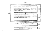
図4を参照すると、フローチャート450は、2段階のDCオフセット補正ウォームアップ・プロセスがいかにして実際的な受信機ウォームアップ・プロセスの1部として使用可能であるかを要約する。ここで、強力なオンまたはオフチャネル信号が閉ループシステムの捕捉性能を劣化させるため、LNA212と送受信スイッチ104は、可能であれば、2段階のDCオフセット補正ウォームアップ・プロセス460、462間に低利得状態にされて、関連するウォームアップ時間を短縮することに注意されたい。ウォームアップ・シーケンス460の第1のステップ間、PMAの入力はアースに短絡されて、ベースバンド路の第1の閉ループ較正を実行する。ウォームアップ・シーケンス462の第2のステップ間、PMA218の入力はミキサ出力に直接接続され、PMAは高利得モードに置かれる。受信路の第2の閉ループ較正は、こうした設定で実行される。高PMA利得設定は、A/D222の入力へのPMA218の入力に存在するオフセットを最大化し、受信感度条件(DC補正性能が最も重要である)下での所望の補正性能を保証することに注意されたい。
Referring to FIG. 4,
DC補正ウォームアップ455後、閉ループDCオフセット補正システムは開ループ補正モード464に置かれ、そのモードにDC補正フィードバック路を保持モードに置くことによって保持され、DC補正値をレジスタ428に保持する。開ループ補正方法を採用して、AGCシステム466の通常動作間、PMA218利得の変更に応答して、開ループ補正を実行することによって瞬時に大きなベースバンドの利得変動により導入されるDCオフセットステップが動的に補償される。
After the DC correction warm-up 455, the closed loop DC offset correction system is placed in the open
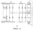
図5は、本発明の好適な実施形態によるPMA218回路形態を示す。PMA218回路形態は、PMA218利得制御範囲全体にのみPMA218段に起因する一定のDCオフセットを達成する。このPMA218段に起因するDCオフセットがPMA218制御範囲を超えて大きく変動する場合、各PMA218利得設定のために追加のウォームアップ較正ステップ310、312が必要とされる。これは、無線装置のバッテリ寿命を最大化するために受信機ウォームアップ時間を最小化する需要があるので、望ましくない。
FIG. 5 illustrates a
利得制御は、演算増幅器510の仮想アースから3dBステップで差動仮想アースへ電流を導くことによって、このPMA218で達成される。DCオフセットへの最大の寄与因子は、演算増幅器510の入力差動段でのミスマッチである。利得制御は増幅器510の前での減衰によって達成されるため、トポロジ512、514はAGC226範囲全体にほぼ一定のDCオフセットを提供する。信号「DCOC」が論理1のとき、PMA218の入力はAC短絡され、共通モード電圧がPMA218の入力に供給されてAGC226の範囲に亘ってラインアップの静的オフセットが算出される。
Gain control is achieved with this
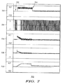
図6、7、および8のグラフは、本発明のDCオフセット補正システムのシステム・シミュレーション結果を示す。図6は、PMA218の利得変動の動的補償がない場合、受信A/D変換器222で生じる可能性がある、200チップ期間(>52us)より長く続く長い過渡電流の例600を示す。PMA218の出力はグラフ602に示され、1−ビットのフィードバック比較器からの出力はグラフ604に示され、DC補正加算器440の出力はグラフ606に示され、受信A/D変換器222の入力はグラフ608に示され、デジタル・オフセット補正D/A変換器232の出力はグラフ610に示される。600では、16dBのPMA218の利得変動が時間612で適用され、LNA212の利得変動を補償する。また、高DCオフセット補正ループ帯域幅は、ループ発振状況を検討することなく、できる限りDC過渡電流を最小化しようと試みる。グラフ608(A/D入力での信号)では、時間612において、高帯域幅モードで動作するループでさえ相当なDC過渡電流(約52us継続時間)があることが分かる。この長い捕捉過渡電流は、16dBのPMAの利得変動に反応しつつ、グラフ608(受信A/D変換器222での信号)における時間612で見ることもできる。このような長いDC過渡電流は、特定のDC過渡電流期間にわたる受信機の性能を劣化させる。
The graphs of FIGS. 6, 7 and 8 show the system simulation results of the DC offset correction system of the present invention. FIG. 6 shows an example 600 of a long transient current that can occur in the receive A /
図7および8は、受信機A/D入力222でのDC過渡電流を除去するためPMA218の入力にのみに存在するオフセットの特定の利得補償アルゴリズムを用いることにより、本発明の2段階のDC補正プロセスの補正動作を強調する700、800を示す。図7を参照すると、PMA218の出力がグラフ702に示され、フィードバック比較器の出力がグラフ704に示され、DC補正減算器440の出力がグラフ706に示され、受信A/D変換器222の入力がグラフ708に示され、デジタル・オフセット補正A/D変換器232の出力がグラフ710に示される。PMA218の後でcal_offsetレジスタ424に、次にウォームアップ・プロセス462に存在するベースバンド路のオフセットを較正し、蓄えるための、期間712間におけるPMA218の入力の短絡が示される。LO215の漏れやミキサ216のオフセット(PMA218入力はミキサ216に接続される)などの受信路に位置する追加オフセットの補正は図7、特にグラフ710の2番目の長い上向きの斜線に見ることができる。時点714で、PMA218の利得は、LNA212の状態の変動を補償するため16dB低減される。さらに、DC補正DAC出力グラフ710は、特定のPMA218の利得変動に起因してPMA218の入力に存在するオフセットのみを補償するため、どのようにして時点714で特定量だけDAC232出力が瞬時に低減されるかを示す。このDC補正DAC232の出力での瞬時開ループ補正の結果、600(図6)で発生した状況とは異なり、グラフ708のA/D222入力には過渡電流がないことに注意されたい。これは、大きなPMA218の利得変動の結果として生じる可能性のある望ましくない過渡電流を除去するための、本発明の開ループ補正アルゴリズムの瞬時補正動作を例示する。
FIGS. 7 and 8 illustrate the two-stage DC correction of the present invention by using an offset specific gain compensation algorithm that is present only at the input of
図8のグラフ800は、PMA218段の後に存在するオフセット(たとえば、IFA、IFF、バイクォッド、出力バッファ、およびDC補正DAC)がPMA218の入力に存在するオフセットより大きい場合ですら、いかにしてDC過渡電流が時点814において受信機A/D222の入力で回避されるかを示す。図6および7と同様、図8は、グラフ802に示されるPMA218の出力、グラフ804に示されるフィードバック比較器の出力、グラフ806に示されるDC補正加算器440の出力、グラフ808に示される受信A/D変換器222の入力、およびグラフ810に示されるデジタル・オフセット補正D/A変換器232の出力を含む。
The
少なくとも1つの例示となる実施形態を上記の本発明の詳細な説明で提示したが、多数の変形が存在することを了解すべきである。さらに、例示となる実施形態は単に例であり、いかなる形でも本発明の範囲、適用可能性、または構造を限定することを意図していないと了解すべきである。そうではなく、上記の詳細な説明は、本発明の例示となる実施形態を実行するための簡便な道筋を当業者に提供するものであり、添付の請求項に記載されるような本発明の範囲を逸脱せずに、例示となる実施形態に記載される構成要素の機能および配置に様々な変更を行うことができると理解される。 While at least one exemplary embodiment has been presented in the foregoing detailed description of the invention, it should be appreciated that a vast number of variations exist. Further, it is to be understood that the illustrated embodiments are merely examples and are not intended to limit the scope, applicability, or structure of the invention in any way. Rather, the above detailed description provides those skilled in the art with a convenient route for carrying out the exemplary embodiments of the invention, and is intended to be the subject of the present invention as set forth in the appended claims. It will be understood that various changes can be made in the function and arrangement of the components described in the exemplary embodiments without departing from the scope.
Claims (20)
前記ベースバンド路の第1の閉ループ補正を実行して、前記DC補正値の第1の成分を得るステップと、
前記受信路の第2の閉ループ補正を前記ウォームアップ時間中の利得に応じて実行し、前記DC補正値の第2の成分を得るステップとを含む、方法。 A method in a radio frequency (RF) receiver circuit having a warm-up time and a receive path associated with the warm-up time, the RF receiver circuit having at least one gain and a baseband path associated with the gain. Including a baseband analog gain control stage, wherein the method performs a DC correction calculation process during the warm-up time to provide a first component and a second component for each of the at least one gain control stage. Obtaining a DC correction value comprising: performing a DC correction calculation process during the warm-up time,
Performing a first closed loop correction of the baseband path to obtain a first component of the DC correction value;
Performing a second closed loop correction of the receive path as a function of the gain during the warm-up time to obtain a second component of the DC correction value.
前記DC補正フィードバック路を保持モードに置くステップと、
利得の変更に応答して、前記DC補正値に応じて開ループ補正を実行するステップとを備える請求項2に記載の方法。 The RF receiver circuit includes a DC correction feedback path, and performing the open loop correction places the DC correction feedback path in a hold mode;
The method of claim 2, comprising performing open loop correction in response to the change in gain in response to the DC correction value.
前記少なくとも1つのベースバンド・アナログ制御段の入力をアースに接続するステップと、
ベースバンド路の閉ループDCオフセット値をDC補正値の第1の成分として記憶するステップと、を備える請求項1に記載の方法。 The at least one baseband analog control stage includes an input and an output, and performing the first closed-loop correction to obtain a first component of the DC correction value;
Connecting the input of the at least one baseband analog control stage to ground;
Storing the baseband closed-loop DC offset value as a first component of the DC correction value.
前記少なくとも1つのミキサの出力を前記少なくとも1つのベースバンド・アナログ利得段の入力と結合するステップと、
前記少なくとも1つのベースバンド・アナログ利得段の利得を高利得に設定するステップと、
前記LNAを低利得状態に置くステップと、
前記受信路の閉ループDCオフセット値を前記DC補正値の第2の成分として記憶するステップと、を備える請求項4に記載の方法。 The RF receiver circuit is coupled to the at least one baseband analog control stage and includes a low noise amplifier (LNA) having a high gain state and a low gain state, and at least one mixer coupled to the LNA. Each of the at least one mixer includes at least one mixer having an input and an output, and performing the second closed-loop correction as a function of gain during the warm-up time, Obtaining two components comprises:
Combining the output of the at least one mixer with the input of the at least one baseband analog gain stage;
Setting the gain of the at least one baseband analog gain stage to a high gain;
Placing the LNA in a low gain state;
Storing the closed-loop DC offset value of the receive path as a second component of the DC correction value.
前記DC補正フィードバック路を保持モードに置くステップと、
自動利得制御の動作を可能にするステップと、
開ループ補正を利得および記憶されたDC補正値に応じて実行するステップと、を備える請求項8に記載の方法。 The RF receiver circuit further includes a DC correction feedback path and performing the open loop correction;
Placing the DC correction feedback path in hold mode;
Enabling automatic gain control operation; and
The method of claim 8, comprising performing open loop correction as a function of gain and stored DC correction value.
前記プレミキサRFラインアップを前記少なくとも1つのベースバンド・アナログ利得段の入力に結合するステップと、
前記少なくとも1つのベースバンド・アナログ利得段の利得を高利得に設定するステップと、
前記プレミキサRFラインアップの利得を低利得状態に設定するステップと、
第2の閉ループDCオフセット値を前記DC補正値の第2の成分として記憶するステップと、を備える請求項1に記載の方法。 The RF receiver circuit is coupled to the at least one baseband analog gain stage and includes a premixer RF lineup having a high gain state and a low gain state, the at least one baseband analog gain stage being an input And performing the second closed loop correction according to the gain during the warm-up time to obtain a second component of the DC correction value,
Coupling the premixer RF lineup to an input of the at least one baseband analog gain stage;
Setting the gain of the at least one baseband analog gain stage to a high gain;
Setting the gain of the premixer RF lineup to a low gain state;
Storing a second closed loop DC offset value as a second component of the DC correction value.
少なくとも1つのベースバンド・アナログ利得制御段であって、該少なくとも1つのベースバンド・アナログ利得制御段に関連する利得を有するとともに、該利得を制御する制御信号を受信するための第1の入力と、第2の入力と、出力とを有する少なくとも1つのベースバンド・アナログ利得制御段と、
前記少なくとも1つの利得制御段に結合され、前記制御信号を生成し前記少なくとも1つの利得制御段に供給するための自動利得制御回路と、
前記少なくとも1つの利得制御段に結合され、該少なくとも1つの利得制御段からの情報を受信するためのるDCオフセット補正回路と、を備え、
前記ウォームアップ時間中、前記少なくとも1つの利得制御段の第2の入力がアースに結合されて、第1の閉ループ補正が実行されてDC補正値の第1の成分が得られ、該DC補正値の第1の成分が前記DCオフセット補正回路に記憶される、RF受信機回路。 A radio frequency (RF) receiver circuit, wherein the RF receiver circuit has a warm-up time associated with the RF receiver circuit.
At least one baseband analog gain control stage having a gain associated with the at least one baseband analog gain control stage and receiving a control signal for controlling the gain; At least one baseband analog gain control stage having a second input and an output;
An automatic gain control circuit coupled to the at least one gain control stage for generating the control signal and supplying the control signal to the at least one gain control stage;
A DC offset correction circuit coupled to the at least one gain control stage and for receiving information from the at least one gain control stage;
During the warm-up time, a second input of the at least one gain control stage is coupled to ground and a first closed loop correction is performed to obtain a first component of a DC correction value, the DC correction value. An RF receiver circuit, wherein a first component of is stored in the DC offset correction circuit.
少なくとも1つのミキサと、を備え、
前記少なくとも1つのミキサの各々は、前記LOに結合される入力と、前記少なくとも1つのベースバンド・アナログ利得制御段のうちの1つに結合可能な出力とを有し、
前記ウォームアップ時間中、前記少なくとも1つの利得制御段の各々の第2の入力は前記少なくとも1つのミキサのうちの1つと結合されて、第2の閉ループ補正が利得に応じて実行されてDC補正値の第2の成分が得られる、請求項14に記載のRF受信機回路。 A low-frequency oscillator (LO),
And at least one mixer,
Each of the at least one mixer has an input coupled to the LO and an output coupleable to one of the at least one baseband analog gain control stages;
During the warm-up time, a second input of each of the at least one gain control stage is coupled with one of the at least one mixer, and a second closed loop correction is performed as a function of gain to provide a DC correction. 15. The RF receiver circuit of claim 14, wherein a second component of value is obtained.
前記LOに結合される入力と、前記利得制御段に結合可能な出力とを有するミキサと、を備え、
前記ウォームアップ時間中、前記少なくとも1つの利得制御段の第2の入力が前記ミキサに結合されて、第2の閉ループ補正が利得に応じて実行されて、2つの部分の2番目について前記DC補正値の第2の成分が得られる、請求項14に記載のRF受信機回路。 A low-frequency oscillator (LO),
A mixer having an input coupled to the LO and an output coupleable to the gain control stage;
During the warm-up time, a second input of the at least one gain control stage is coupled to the mixer, and a second closed-loop correction is performed as a function of gain, and the DC correction for the second of the two parts. 15. The RF receiver circuit of claim 14, wherein a second component of value is obtained.
Applications Claiming Priority (2)
| Application Number | Priority Date | Filing Date | Title |
|---|---|---|---|
| US11/099,138 US7899431B2 (en) | 2005-04-04 | 2005-04-04 | DC offset correction system for a receiver with baseband gain control |
| PCT/US2006/007120 WO2006107466A2 (en) | 2005-04-04 | 2006-02-28 | Dc offset correction system for a receiver with baseband gain control |
Publications (2)
| Publication Number | Publication Date |
|---|---|
| JP2008535377A true JP2008535377A (en) | 2008-08-28 |
| JP2008535377A5 JP2008535377A5 (en) | 2009-04-09 |
Family
ID=37070476
Family Applications (1)
| Application Number | Title | Priority Date | Filing Date |
|---|---|---|---|
| JP2008504060A Pending JP2008535377A (en) | 2005-04-04 | 2006-02-28 | DC offset correction system for a receiver with baseband gain control |
Country Status (5)
| Country | Link |
|---|---|
| US (1) | US7899431B2 (en) |
| EP (1) | EP1869855B8 (en) |
| JP (1) | JP2008535377A (en) |
| KR (1) | KR101241064B1 (en) |
| WO (1) | WO2006107466A2 (en) |
Families Citing this family (22)
| Publication number | Priority date | Publication date | Assignee | Title |
|---|---|---|---|---|
| US7277688B2 (en) * | 2003-06-17 | 2007-10-02 | Broadcom Corporation | DC offset correction for very low intermediate frequency receiver |
| JP4403132B2 (en) * | 2005-11-11 | 2010-01-20 | 株式会社東芝 | Receiving machine |
| US7603094B2 (en) * | 2006-06-14 | 2009-10-13 | Freescale Semiconductor Inc. | DC offset correction for direct conversion receivers |
| US8195096B2 (en) * | 2006-07-13 | 2012-06-05 | Mediatek Inc. | Apparatus and method for enhancing DC offset correction speed of a radio device |
| US7912437B2 (en) * | 2007-01-09 | 2011-03-22 | Freescale Semiconductor, Inc. | Radio frequency receiver having dynamic bandwidth control and method of operation |
| US8010077B2 (en) * | 2008-04-21 | 2011-08-30 | Freescale Semiconductor, Inc. | DC offset calibration in a direct conversion receiver |
| US8260227B2 (en) * | 2008-06-10 | 2012-09-04 | Mediatek Inc. | Direct conversion receiver and DC offset concellation method |
| US8170506B2 (en) * | 2008-07-29 | 2012-05-01 | Qualcomm Incorporated | Direct current (DC) offset correction using analog-to-digital conversion |
| US8494470B2 (en) | 2008-11-25 | 2013-07-23 | Silicon Laboratories Inc. | Integrated receivers and integrated circuit having integrated inductors |
| US8306103B2 (en) * | 2009-12-07 | 2012-11-06 | Csr Technology Inc. | Systems and methods providing in-phase and quadrature equalization |
| GB2487973A (en) * | 2011-02-11 | 2012-08-15 | Elonics Ltd | Reduction of DC offsets in high gain cross-coupled IF active filters |
| US8983417B2 (en) | 2012-01-03 | 2015-03-17 | Silicon Laboratories Inc. | Low-cost receiver using integrated inductors |
| CN103312647B (en) | 2012-03-08 | 2017-07-04 | 英特尔德国有限责任公司 | For the method for fine RF transceiver direct current offset calibration |
| EP2637311B1 (en) * | 2012-03-08 | 2016-12-07 | Intel Deutschland GmbH | Algorithm for raw rf transceiver dc offset calibration |
| EP2637312B1 (en) * | 2012-03-08 | 2017-01-11 | Intel Deutschland GmbH | Algorithm for fine rf transceiver dc offset calibration |
| US8787503B2 (en) * | 2012-09-18 | 2014-07-22 | Vixs Systems, Inc. | Frequency mixer with compensated DC offset correction to reduce linearity degradation |
| US10079647B2 (en) * | 2014-12-10 | 2018-09-18 | Nxp Usa, Inc. | DC offset calibration of wireless receivers |
| EP3068044A1 (en) * | 2015-03-11 | 2016-09-14 | Nxp B.V. | Module for a radio receiver |
| US9608587B2 (en) | 2015-06-25 | 2017-03-28 | Freescale Semiconductor, Inc. | Systems and methods to dynamically calibrate and adjust gains in a direct conversion receiver |
| US9577576B1 (en) | 2016-06-22 | 2017-02-21 | Qualcomm Incorporated | Biased passive mixer |
| US10382087B1 (en) * | 2018-12-14 | 2019-08-13 | Texas Instruments Incorporated | Adaptation of zero intermediate frequency (ZIF) transmitter to correct local oscillator (LO) leakage |
| KR102543126B1 (en) * | 2020-09-29 | 2023-06-13 | 홍성준 | Meat sauce containing yeast and fermenting apparatus of the meat sauce containing yeast |
Citations (1)
| Publication number | Priority date | Publication date | Assignee | Title |
|---|---|---|---|---|
| JP2005020119A (en) * | 2003-06-24 | 2005-01-20 | Renesas Technology Corp | Semiconductor integrated circuit for communication, wireless communication system, and adjustment method of gain and offset |
Family Cites Families (19)
| Publication number | Priority date | Publication date | Assignee | Title |
|---|---|---|---|---|
| US5251233A (en) | 1990-12-20 | 1993-10-05 | Motorola, Inc. | Apparatus and method for equalizing a corrupted signal in a receiver |
| US5212826A (en) * | 1990-12-20 | 1993-05-18 | Motorola, Inc. | Apparatus and method of dc offset correction for a receiver |
| US5689815A (en) | 1995-05-04 | 1997-11-18 | Oki Telecom, Inc. | Saturation prevention system for radio telephone with open and closed loop power control systems |
| US6240100B1 (en) * | 1997-07-31 | 2001-05-29 | Motorola, Inc. | Cellular TDMA base station receiver with dynamic DC offset correction |
| US6504884B1 (en) * | 1999-05-12 | 2003-01-07 | Analog Devices, Inc. | Method for correcting DC offsets in a receiver |
| US6459889B1 (en) * | 2000-02-29 | 2002-10-01 | Motorola, Inc. | DC offset correction loop for radio receiver |
| US6668164B2 (en) | 2000-06-01 | 2003-12-23 | Motorola, Inc. | Method and apparatus for reducing intermodulation distortion in a low current drain automatic gain control system |
| US6606359B1 (en) * | 2000-07-26 | 2003-08-12 | Motorola, Inc | Area-optimum rapid acquisition cellular multi-protocol digital DC offset correction scheme |
| US6735422B1 (en) * | 2000-10-02 | 2004-05-11 | Baldwin Keith R | Calibrated DC compensation system for a wireless communication device configured in a zero intermediate frequency architecture |
| US6560447B2 (en) * | 2001-03-05 | 2003-05-06 | Motorola, Inc. | DC offset correction scheme for wireless receivers |
| DE10128236A1 (en) * | 2001-06-11 | 2002-08-01 | Infineon Technologies Ag | Method for compensating a step-shaped DC interference in a digital baseband signal of a homodyne radio receiver |
| JP3805258B2 (en) * | 2002-01-29 | 2006-08-02 | 松下電器産業株式会社 | Direct conversion receiver |
| US7385913B2 (en) * | 2002-04-24 | 2008-06-10 | Motorola, Inc. | Method and apparatus for compensating for variations in a receive portion of a wireless communication device |
| US6753727B2 (en) * | 2002-06-13 | 2004-06-22 | Skyworks Solutions, Inc. | Sequential DC offset correction for amplifier chain |
| US7136431B2 (en) * | 2002-10-24 | 2006-11-14 | Broadcom Corporation | DC offset correcting in a direct conversion or very low IF receiver |
| US7333557B2 (en) * | 2002-12-16 | 2008-02-19 | Nortel Networks Limited | Adaptive controller for linearization of transmitter with impairments |
| JP4230762B2 (en) * | 2002-12-20 | 2009-02-25 | 株式会社ルネサステクノロジ | Direct conversion receiver |
| US7302246B2 (en) * | 2002-12-23 | 2007-11-27 | Intel Corporation | Programmable gain amplifier with self-adjusting offset correction |
| US6750703B1 (en) * | 2002-12-24 | 2004-06-15 | Silicon Integrated Systems Corp. | DC offset canceling circuit applied in a variable gain amplifier |
-
2005
- 2005-04-04 US US11/099,138 patent/US7899431B2/en active Active
-
2006
- 2006-02-28 JP JP2008504060A patent/JP2008535377A/en active Pending
- 2006-02-28 EP EP06736439.8A patent/EP1869855B8/en not_active Expired - Fee Related
- 2006-02-28 KR KR1020077022679A patent/KR101241064B1/en active IP Right Grant
- 2006-02-28 WO PCT/US2006/007120 patent/WO2006107466A2/en active Application Filing
Patent Citations (1)
| Publication number | Priority date | Publication date | Assignee | Title |
|---|---|---|---|---|
| JP2005020119A (en) * | 2003-06-24 | 2005-01-20 | Renesas Technology Corp | Semiconductor integrated circuit for communication, wireless communication system, and adjustment method of gain and offset |
Also Published As
| Publication number | Publication date |
|---|---|
| KR101241064B1 (en) | 2013-03-12 |
| EP1869855B8 (en) | 2016-06-01 |
| KR20080002806A (en) | 2008-01-04 |
| EP1869855B1 (en) | 2016-04-27 |
| EP1869855A2 (en) | 2007-12-26 |
| US7899431B2 (en) | 2011-03-01 |
| US20060222117A1 (en) | 2006-10-05 |
| WO2006107466A2 (en) | 2006-10-12 |
| EP1869855A4 (en) | 2013-05-01 |
| WO2006107466A3 (en) | 2007-11-15 |
Similar Documents
| Publication | Publication Date | Title |
|---|---|---|
| JP2008535377A (en) | DC offset correction system for a receiver with baseband gain control | |
| EP1878184B1 (en) | Power control system for a continuous time mobile transmitter | |
| EP2386144B1 (en) | Circuits, systems, and methods for managing automatic gain control in quadrature signal paths of a receiver | |
| US7912437B2 (en) | Radio frequency receiver having dynamic bandwidth control and method of operation | |
| US8666343B2 (en) | DC-offset-correction system and method for communication receivers | |
| US9065537B2 (en) | Method and system for calibrating a multi-mode, multi-standard transmitter and receiver | |
| US7346317B2 (en) | Dynamic gain and phase compensation for power amplifier load switching | |
| US7409199B2 (en) | Direct conversion receiver with DC offset compensation | |
| US20030174783A1 (en) | Self calibrating transmit path correction system | |
| EP2055013B1 (en) | Adaptive predistortion for controlling an open loop power amplifier | |
| EP1902525A2 (en) | Polar loop radio frequency (rf) transmitter having increased dynamic range amplitude control | |
| US20060227910A1 (en) | Receiver DC offset correction | |
| US7149487B2 (en) | Mobile communication terminal device and variable gain circuit | |
| US7496163B2 (en) | AGC system, AGC method, and receiver using the AGC system | |
| US7110724B1 (en) | System and method for detecting compression of a power amplifier circuit | |
| JP5098811B2 (en) | Portable terminal device and power consumption control method thereof | |
| US20240106467A1 (en) | Envelope tracking for radio frequency (rf) front end modules | |
| KR100592589B1 (en) | Apparatus and method for automatic gain control to suppress the generation of inter-modulation products in receiver | |
| KR100644550B1 (en) | Method for calibrating control parameter of transmission power in global system for mobile communication terminal and the terminal thereof |
Legal Events
| Date | Code | Title | Description |
|---|---|---|---|
| A521 | Written amendment |
Free format text: JAPANESE INTERMEDIATE CODE: A523 Effective date: 20090218 |
|
| A621 | Written request for application examination |
Free format text: JAPANESE INTERMEDIATE CODE: A621 Effective date: 20090218 |
|
| A977 | Report on retrieval |
Free format text: JAPANESE INTERMEDIATE CODE: A971007 Effective date: 20101119 |
|
| A131 | Notification of reasons for refusal |
Free format text: JAPANESE INTERMEDIATE CODE: A131 Effective date: 20101207 |
|
| A601 | Written request for extension of time |
Free format text: JAPANESE INTERMEDIATE CODE: A601 Effective date: 20110303 Free format text: JAPANESE INTERMEDIATE CODE: A601 Effective date: 20110303 |
|
| A602 | Written permission of extension of time |
Free format text: JAPANESE INTERMEDIATE CODE: A602 Effective date: 20110310 |
|
| A521 | Written amendment |
Free format text: JAPANESE INTERMEDIATE CODE: A523 Effective date: 20110406 |
|
| A02 | Decision of refusal |
Free format text: JAPANESE INTERMEDIATE CODE: A02 Effective date: 20110809 Free format text: JAPANESE INTERMEDIATE CODE: A02 Effective date: 20110809 |