JP2008527375A - Infrared transmitting substrate, semiconductor substrate, silicon substrate, fluid sample analysis device, fluid sample analysis method, and computer-readable recording medium - Google Patents
Infrared transmitting substrate, semiconductor substrate, silicon substrate, fluid sample analysis device, fluid sample analysis method, and computer-readable recording medium Download PDFInfo
- Publication number
- JP2008527375A JP2008527375A JP2007551259A JP2007551259A JP2008527375A JP 2008527375 A JP2008527375 A JP 2008527375A JP 2007551259 A JP2007551259 A JP 2007551259A JP 2007551259 A JP2007551259 A JP 2007551259A JP 2008527375 A JP2008527375 A JP 2008527375A
- Authority
- JP
- Japan
- Prior art keywords
- sample
- fluid sample
- substrate
- probe
- infrared
- Prior art date
- Legal status (The legal status is an assumption and is not a legal conclusion. Google has not performed a legal analysis and makes no representation as to the accuracy of the status listed.)
- Pending
Links
- 239000000758 substrate Substances 0.000 title claims abstract description 107
- 238000004458 analytical method Methods 0.000 title claims abstract description 43
- 239000012530 fluid Substances 0.000 title claims description 128
- 239000004065 semiconductor Substances 0.000 title claims description 29
- 229910052710 silicon Inorganic materials 0.000 title claims description 27
- XUIMIQQOPSSXEZ-UHFFFAOYSA-N Silicon Chemical compound [Si] XUIMIQQOPSSXEZ-UHFFFAOYSA-N 0.000 title claims description 24
- 239000010703 silicon Substances 0.000 title claims description 24
- 238000012284 sample analysis method Methods 0.000 title claims 13
- 239000000523 sample Substances 0.000 claims abstract description 442
- 239000012472 biological sample Substances 0.000 claims abstract description 50
- 238000000034 method Methods 0.000 claims description 87
- 238000000862 absorption spectrum Methods 0.000 claims description 41
- 238000010521 absorption reaction Methods 0.000 claims description 28
- 239000000463 material Substances 0.000 claims description 26
- 238000001514 detection method Methods 0.000 claims description 21
- 230000005540 biological transmission Effects 0.000 claims description 16
- 238000003860 storage Methods 0.000 claims description 15
- 230000001678 irradiating effect Effects 0.000 claims 2
- 235000012431 wafers Nutrition 0.000 description 95
- 230000003287 optical effect Effects 0.000 description 29
- 230000009102 absorption Effects 0.000 description 21
- 238000000926 separation method Methods 0.000 description 21
- 238000012360 testing method Methods 0.000 description 21
- 230000003595 spectral effect Effects 0.000 description 18
- 239000000126 substance Substances 0.000 description 18
- 238000005259 measurement Methods 0.000 description 17
- 102000004169 proteins and genes Human genes 0.000 description 16
- 108090000623 proteins and genes Proteins 0.000 description 16
- 238000004566 IR spectroscopy Methods 0.000 description 14
- 230000027455 binding Effects 0.000 description 13
- 230000005855 radiation Effects 0.000 description 13
- 238000001228 spectrum Methods 0.000 description 13
- 230000003993 interaction Effects 0.000 description 11
- 230000008569 process Effects 0.000 description 11
- 238000012545 processing Methods 0.000 description 11
- 230000000694 effects Effects 0.000 description 10
- 238000003556 assay Methods 0.000 description 9
- 230000005684 electric field Effects 0.000 description 9
- 238000005070 sampling Methods 0.000 description 9
- 230000033001 locomotion Effects 0.000 description 8
- 150000001875 compounds Chemical class 0.000 description 7
- 238000010586 diagram Methods 0.000 description 7
- 238000002474 experimental method Methods 0.000 description 7
- 238000001155 isoelectric focusing Methods 0.000 description 7
- 210000004027 cell Anatomy 0.000 description 6
- 239000003814 drug Substances 0.000 description 6
- 238000006243 chemical reaction Methods 0.000 description 5
- 229940079593 drug Drugs 0.000 description 5
- 238000005530 etching Methods 0.000 description 5
- 238000003384 imaging method Methods 0.000 description 5
- 230000031700 light absorption Effects 0.000 description 5
- 230000006916 protein interaction Effects 0.000 description 5
- 238000002460 vibrational spectroscopy Methods 0.000 description 5
- XLYOFNOQVPJJNP-UHFFFAOYSA-N water Substances O XLYOFNOQVPJJNP-UHFFFAOYSA-N 0.000 description 5
- IJGRMHOSHXDMSA-UHFFFAOYSA-N Atomic nitrogen Chemical compound N#N IJGRMHOSHXDMSA-UHFFFAOYSA-N 0.000 description 4
- CURLTUGMZLYLDI-UHFFFAOYSA-N Carbon dioxide Chemical compound O=C=O CURLTUGMZLYLDI-UHFFFAOYSA-N 0.000 description 4
- 238000007792 addition Methods 0.000 description 4
- 239000011248 coating agent Substances 0.000 description 4
- 238000000576 coating method Methods 0.000 description 4
- 238000005516 engineering process Methods 0.000 description 4
- 238000001704 evaporation Methods 0.000 description 4
- 230000008020 evaporation Effects 0.000 description 4
- -1 halide salts Chemical class 0.000 description 4
- 239000011159 matrix material Substances 0.000 description 4
- 108090000790 Enzymes Proteins 0.000 description 3
- 102000004190 Enzymes Human genes 0.000 description 3
- VYPSYNLAJGMNEJ-UHFFFAOYSA-N Silicium dioxide Chemical compound O=[Si]=O VYPSYNLAJGMNEJ-UHFFFAOYSA-N 0.000 description 3
- HEMHJVSKTPXQMS-UHFFFAOYSA-M Sodium hydroxide Chemical compound [OH-].[Na+] HEMHJVSKTPXQMS-UHFFFAOYSA-M 0.000 description 3
- 239000007864 aqueous solution Substances 0.000 description 3
- 230000008901 benefit Effects 0.000 description 3
- 230000008238 biochemical pathway Effects 0.000 description 3
- 230000008859 change Effects 0.000 description 3
- 239000007795 chemical reaction product Substances 0.000 description 3
- 239000012636 effector Substances 0.000 description 3
- 229920001971 elastomer Polymers 0.000 description 3
- 238000001962 electrophoresis Methods 0.000 description 3
- 229910052732 germanium Inorganic materials 0.000 description 3
- 239000003446 ligand Substances 0.000 description 3
- 230000004001 molecular interaction Effects 0.000 description 3
- 230000009467 reduction Effects 0.000 description 3
- 238000012216 screening Methods 0.000 description 3
- 239000007787 solid Substances 0.000 description 3
- 239000000243 solution Substances 0.000 description 3
- 238000000935 solvent evaporation Methods 0.000 description 3
- 238000004611 spectroscopical analysis Methods 0.000 description 3
- 238000002965 ELISA Methods 0.000 description 2
- NBIIXXVUZAFLBC-UHFFFAOYSA-N Phosphoric acid Chemical compound OP(O)(O)=O NBIIXXVUZAFLBC-UHFFFAOYSA-N 0.000 description 2
- WCUXLLCKKVVCTQ-UHFFFAOYSA-M Potassium chloride Chemical compound [Cl-].[K+] WCUXLLCKKVVCTQ-UHFFFAOYSA-M 0.000 description 2
- FAPWRFPIFSIZLT-UHFFFAOYSA-M Sodium chloride Chemical compound [Na+].[Cl-] FAPWRFPIFSIZLT-UHFFFAOYSA-M 0.000 description 2
- 230000002378 acidificating effect Effects 0.000 description 2
- 239000000654 additive Substances 0.000 description 2
- 230000004075 alteration Effects 0.000 description 2
- 150000001413 amino acids Chemical class 0.000 description 2
- 238000003491 array Methods 0.000 description 2
- 239000001569 carbon dioxide Substances 0.000 description 2
- 229910002092 carbon dioxide Inorganic materials 0.000 description 2
- 210000000170 cell membrane Anatomy 0.000 description 2
- 239000003795 chemical substances by application Substances 0.000 description 2
- 230000001276 controlling effect Effects 0.000 description 2
- 230000000875 corresponding effect Effects 0.000 description 2
- 238000000708 deep reactive-ion etching Methods 0.000 description 2
- 229910001873 dinitrogen Inorganic materials 0.000 description 2
- 239000000806 elastomer Substances 0.000 description 2
- 238000005370 electroosmosis Methods 0.000 description 2
- 239000010408 film Substances 0.000 description 2
- 239000011521 glass Substances 0.000 description 2
- 238000010438 heat treatment Methods 0.000 description 2
- 230000003834 intracellular effect Effects 0.000 description 2
- 238000002372 labelling Methods 0.000 description 2
- 239000007788 liquid Substances 0.000 description 2
- 102000006240 membrane receptors Human genes 0.000 description 2
- 108020004084 membrane receptors Proteins 0.000 description 2
- 239000000203 mixture Substances 0.000 description 2
- 239000004033 plastic Substances 0.000 description 2
- 229920003023 plastic Polymers 0.000 description 2
- 229920000642 polymer Polymers 0.000 description 2
- 229920001343 polytetrafluoroethylene Polymers 0.000 description 2
- 239000004810 polytetrafluoroethylene Substances 0.000 description 2
- 239000000843 powder Substances 0.000 description 2
- 238000002360 preparation method Methods 0.000 description 2
- 238000003127 radioimmunoassay Methods 0.000 description 2
- 239000000376 reactant Substances 0.000 description 2
- 102000005962 receptors Human genes 0.000 description 2
- 108020003175 receptors Proteins 0.000 description 2
- SBIBMFFZSBJNJF-UHFFFAOYSA-N selenium;zinc Chemical compound [Se]=[Zn] SBIBMFFZSBJNJF-UHFFFAOYSA-N 0.000 description 2
- 230000035945 sensitivity Effects 0.000 description 2
- HBMJWWWQQXIZIP-UHFFFAOYSA-N silicon carbide Chemical compound [Si+]#[C-] HBMJWWWQQXIZIP-UHFFFAOYSA-N 0.000 description 2
- 229910010271 silicon carbide Inorganic materials 0.000 description 2
- 235000012239 silicon dioxide Nutrition 0.000 description 2
- 150000003384 small molecules Chemical class 0.000 description 2
- 238000006467 substitution reaction Methods 0.000 description 2
- 239000012780 transparent material Substances 0.000 description 2
- KHOITXIGCFIULA-UHFFFAOYSA-N Alophen Chemical compound C1=CC(OC(=O)C)=CC=C1C(C=1N=CC=CC=1)C1=CC=C(OC(C)=O)C=C1 KHOITXIGCFIULA-UHFFFAOYSA-N 0.000 description 1
- 108010032595 Antibody Binding Sites Proteins 0.000 description 1
- 229910016036 BaF 2 Inorganic materials 0.000 description 1
- 230000005457 Black-body radiation Effects 0.000 description 1
- 229910004261 CaF 2 Inorganic materials 0.000 description 1
- IGXWBGJHJZYPQS-SSDOTTSWSA-N D-Luciferin Chemical compound OC(=O)[C@H]1CSC(C=2SC3=CC=C(O)C=C3N=2)=N1 IGXWBGJHJZYPQS-SSDOTTSWSA-N 0.000 description 1
- CYCGRDQQIOGCKX-UHFFFAOYSA-N Dehydro-luciferin Natural products OC(=O)C1=CSC(C=2SC3=CC(O)=CC=C3N=2)=N1 CYCGRDQQIOGCKX-UHFFFAOYSA-N 0.000 description 1
- IMROMDMJAWUWLK-UHFFFAOYSA-N Ethenol Chemical compound OC=C IMROMDMJAWUWLK-UHFFFAOYSA-N 0.000 description 1
- BJGNCJDXODQBOB-UHFFFAOYSA-N Fivefly Luciferin Natural products OC(=O)C1CSC(C=2SC3=CC(O)=CC=C3N=2)=N1 BJGNCJDXODQBOB-UHFFFAOYSA-N 0.000 description 1
- 238000005033 Fourier transform infrared spectroscopy Methods 0.000 description 1
- 229910001218 Gallium arsenide Inorganic materials 0.000 description 1
- DGAQECJNVWCQMB-PUAWFVPOSA-M Ilexoside XXIX Chemical compound C[C@@H]1CC[C@@]2(CC[C@@]3(C(=CC[C@H]4[C@]3(CC[C@@H]5[C@@]4(CC[C@@H](C5(C)C)OS(=O)(=O)[O-])C)C)[C@@H]2[C@]1(C)O)C)C(=O)O[C@H]6[C@@H]([C@H]([C@@H]([C@H](O6)CO)O)O)O.[Na+] DGAQECJNVWCQMB-PUAWFVPOSA-M 0.000 description 1
- 108060001084 Luciferase Proteins 0.000 description 1
- 239000005089 Luciferase Substances 0.000 description 1
- DDWFXDSYGUXRAY-UHFFFAOYSA-N Luciferin Natural products CCc1c(C)c(CC2NC(=O)C(=C2C=C)C)[nH]c1Cc3[nH]c4C(=C5/NC(CC(=O)O)C(C)C5CC(=O)O)CC(=O)c4c3C DDWFXDSYGUXRAY-UHFFFAOYSA-N 0.000 description 1
- 108010052285 Membrane Proteins Proteins 0.000 description 1
- 102000018697 Membrane Proteins Human genes 0.000 description 1
- 229910000661 Mercury cadmium telluride Inorganic materials 0.000 description 1
- 102000029749 Microtubule Human genes 0.000 description 1
- 108091022875 Microtubule Proteins 0.000 description 1
- 239000004698 Polyethylene Substances 0.000 description 1
- 230000010799 Receptor Interactions Effects 0.000 description 1
- 239000004809 Teflon Substances 0.000 description 1
- 229920006362 Teflon® Polymers 0.000 description 1
- 229920004890 Triton X-100 Polymers 0.000 description 1
- 239000013504 Triton X-100 Substances 0.000 description 1
- XSQUKJJJFZCRTK-UHFFFAOYSA-N Urea Chemical compound NC(N)=O XSQUKJJJFZCRTK-UHFFFAOYSA-N 0.000 description 1
- 239000003929 acidic solution Substances 0.000 description 1
- 230000009471 action Effects 0.000 description 1
- 230000000996 additive effect Effects 0.000 description 1
- 230000002411 adverse Effects 0.000 description 1
- 239000003513 alkali Substances 0.000 description 1
- 229910000147 aluminium phosphate Inorganic materials 0.000 description 1
- 239000012080 ambient air Substances 0.000 description 1
- 239000000959 ampholyte mixture Substances 0.000 description 1
- 230000003321 amplification Effects 0.000 description 1
- 239000012491 analyte Substances 0.000 description 1
- 239000000427 antigen Substances 0.000 description 1
- 102000036639 antigens Human genes 0.000 description 1
- 108091007433 antigens Proteins 0.000 description 1
- 238000013459 approach Methods 0.000 description 1
- 239000003125 aqueous solvent Substances 0.000 description 1
- 239000012298 atmosphere Substances 0.000 description 1
- 239000002585 base Substances 0.000 description 1
- 239000003637 basic solution Substances 0.000 description 1
- 230000009141 biological interaction Effects 0.000 description 1
- 239000004202 carbamide Substances 0.000 description 1
- 230000001413 cellular effect Effects 0.000 description 1
- 238000012512 characterization method Methods 0.000 description 1
- 230000002925 chemical effect Effects 0.000 description 1
- 238000007398 colorimetric assay Methods 0.000 description 1
- 238000004891 communication Methods 0.000 description 1
- 230000006854 communication Effects 0.000 description 1
- 238000003271 compound fluorescence assay Methods 0.000 description 1
- 239000012141 concentrate Substances 0.000 description 1
- 230000021615 conjugation Effects 0.000 description 1
- 238000007796 conventional method Methods 0.000 description 1
- 230000002596 correlated effect Effects 0.000 description 1
- 229910021419 crystalline silicon Inorganic materials 0.000 description 1
- 230000007423 decrease Effects 0.000 description 1
- 238000000151 deposition Methods 0.000 description 1
- 238000009795 derivation Methods 0.000 description 1
- 238000013461 design Methods 0.000 description 1
- 230000001066 destructive effect Effects 0.000 description 1
- 239000003599 detergent Substances 0.000 description 1
- 201000010099 disease Diseases 0.000 description 1
- 208000037265 diseases, disorders, signs and symptoms Diseases 0.000 description 1
- 238000007876 drug discovery Methods 0.000 description 1
- 238000007877 drug screening Methods 0.000 description 1
- 230000005670 electromagnetic radiation Effects 0.000 description 1
- 230000007613 environmental effect Effects 0.000 description 1
- 238000006911 enzymatic reaction Methods 0.000 description 1
- 238000013401 experimental design Methods 0.000 description 1
- 238000000605 extraction Methods 0.000 description 1
- 239000000835 fiber Substances 0.000 description 1
- 238000001914 filtration Methods 0.000 description 1
- 230000004907 flux Effects 0.000 description 1
- 235000013305 food Nutrition 0.000 description 1
- 238000009615 fourier-transform spectroscopy Methods 0.000 description 1
- 230000006870 function Effects 0.000 description 1
- 239000007789 gas Substances 0.000 description 1
- 238000001502 gel electrophoresis Methods 0.000 description 1
- 238000009499 grossing Methods 0.000 description 1
- 230000006872 improvement Effects 0.000 description 1
- 238000012844 infrared spectroscopy analysis Methods 0.000 description 1
- 238000002329 infrared spectrum Methods 0.000 description 1
- 238000009413 insulation Methods 0.000 description 1
- 230000001788 irregular Effects 0.000 description 1
- 238000001459 lithography Methods 0.000 description 1
- 238000004949 mass spectrometry Methods 0.000 description 1
- 230000002503 metabolic effect Effects 0.000 description 1
- 229910052751 metal Inorganic materials 0.000 description 1
- 239000002184 metal Substances 0.000 description 1
- 229920000609 methyl cellulose Polymers 0.000 description 1
- 239000001923 methylcellulose Substances 0.000 description 1
- 210000004688 microtubule Anatomy 0.000 description 1
- 238000003330 mid-infrared imaging Methods 0.000 description 1
- 230000005012 migration Effects 0.000 description 1
- 238000013508 migration Methods 0.000 description 1
- 238000002156 mixing Methods 0.000 description 1
- 230000009149 molecular binding Effects 0.000 description 1
- 238000012544 monitoring process Methods 0.000 description 1
- 229910052757 nitrogen Inorganic materials 0.000 description 1
- 238000003199 nucleic acid amplification method Methods 0.000 description 1
- HEGSGKPQLMEBJL-RKQHYHRCSA-N octyl beta-D-glucopyranoside Chemical compound CCCCCCCCO[C@@H]1O[C@H](CO)[C@@H](O)[C@H](O)[C@H]1O HEGSGKPQLMEBJL-RKQHYHRCSA-N 0.000 description 1
- 239000003960 organic solvent Substances 0.000 description 1
- 239000006072 paste Substances 0.000 description 1
- 230000000737 periodic effect Effects 0.000 description 1
- 230000010363 phase shift Effects 0.000 description 1
- 230000000704 physical effect Effects 0.000 description 1
- 229910021420 polycrystalline silicon Inorganic materials 0.000 description 1
- 229920000573 polyethylene Polymers 0.000 description 1
- 229920005591 polysilicon Polymers 0.000 description 1
- 229920002451 polyvinyl alcohol Polymers 0.000 description 1
- 239000001103 potassium chloride Substances 0.000 description 1
- 235000011164 potassium chloride Nutrition 0.000 description 1
- 238000001556 precipitation Methods 0.000 description 1
- 230000002028 premature Effects 0.000 description 1
- 238000007639 printing Methods 0.000 description 1
- 238000011112 process operation Methods 0.000 description 1
- 239000000047 product Substances 0.000 description 1
- 230000004845 protein aggregation Effects 0.000 description 1
- 230000004850 protein–protein interaction Effects 0.000 description 1
- 238000000746 purification Methods 0.000 description 1
- 239000010453 quartz Substances 0.000 description 1
- 229910001404 rare earth metal oxide Inorganic materials 0.000 description 1
- 230000009257 reactivity Effects 0.000 description 1
- 238000011897 real-time detection Methods 0.000 description 1
- 238000011160 research Methods 0.000 description 1
- 230000002441 reversible effect Effects 0.000 description 1
- 238000012552 review Methods 0.000 description 1
- 229910052594 sapphire Inorganic materials 0.000 description 1
- 239000010980 sapphire Substances 0.000 description 1
- 235000015067 sauces Nutrition 0.000 description 1
- 239000000377 silicon dioxide Substances 0.000 description 1
- 239000002210 silicon-based material Substances 0.000 description 1
- 229910052708 sodium Inorganic materials 0.000 description 1
- 239000011734 sodium Substances 0.000 description 1
- 239000011780 sodium chloride Substances 0.000 description 1
- 239000002904 solvent Substances 0.000 description 1
- 238000002798 spectrophotometry method Methods 0.000 description 1
- 238000007811 spectroscopic assay Methods 0.000 description 1
- 230000000087 stabilizing effect Effects 0.000 description 1
- 230000003335 steric effect Effects 0.000 description 1
- 238000005556 structure-activity relationship Methods 0.000 description 1
- PGAPATLGJSQQBU-UHFFFAOYSA-M thallium(i) bromide Chemical compound [Tl]Br PGAPATLGJSQQBU-UHFFFAOYSA-M 0.000 description 1
- 239000010409 thin film Substances 0.000 description 1
- 230000036962 time dependent Effects 0.000 description 1
- 230000009466 transformation Effects 0.000 description 1
- 230000007704 transition Effects 0.000 description 1
- 238000000411 transmission spectrum Methods 0.000 description 1
- 239000001993 wax Substances 0.000 description 1
Images


Classifications
-
- G—PHYSICS
- G01—MEASURING; TESTING
- G01N—INVESTIGATING OR ANALYSING MATERIALS BY DETERMINING THEIR CHEMICAL OR PHYSICAL PROPERTIES
- G01N27/00—Investigating or analysing materials by the use of electric, electrochemical, or magnetic means
- G01N27/26—Investigating or analysing materials by the use of electric, electrochemical, or magnetic means by investigating electrochemical variables; by using electrolysis or electrophoresis
- G01N27/416—Systems
- G01N27/447—Systems using electrophoresis
- G01N27/44704—Details; Accessories
- G01N27/44717—Arrangements for investigating the separated zones, e.g. localising zones
- G01N27/44721—Arrangements for investigating the separated zones, e.g. localising zones by optical means
-
- G—PHYSICS
- G01—MEASURING; TESTING
- G01N—INVESTIGATING OR ANALYSING MATERIALS BY DETERMINING THEIR CHEMICAL OR PHYSICAL PROPERTIES
- G01N21/00—Investigating or analysing materials by the use of optical means, i.e. using sub-millimetre waves, infrared, visible or ultraviolet light
- G01N21/01—Arrangements or apparatus for facilitating the optical investigation
- G01N21/03—Cuvette constructions
-
- G—PHYSICS
- G01—MEASURING; TESTING
- G01N—INVESTIGATING OR ANALYSING MATERIALS BY DETERMINING THEIR CHEMICAL OR PHYSICAL PROPERTIES
- G01N21/00—Investigating or analysing materials by the use of optical means, i.e. using sub-millimetre waves, infrared, visible or ultraviolet light
- G01N21/17—Systems in which incident light is modified in accordance with the properties of the material investigated
- G01N21/25—Colour; Spectral properties, i.e. comparison of effect of material on the light at two or more different wavelengths or wavelength bands
- G01N21/251—Colorimeters; Construction thereof
- G01N21/253—Colorimeters; Construction thereof for batch operation, i.e. multisample apparatus
-
- G—PHYSICS
- G01—MEASURING; TESTING
- G01N—INVESTIGATING OR ANALYSING MATERIALS BY DETERMINING THEIR CHEMICAL OR PHYSICAL PROPERTIES
- G01N21/00—Investigating or analysing materials by the use of optical means, i.e. using sub-millimetre waves, infrared, visible or ultraviolet light
- G01N21/17—Systems in which incident light is modified in accordance with the properties of the material investigated
- G01N21/25—Colour; Spectral properties, i.e. comparison of effect of material on the light at two or more different wavelengths or wavelength bands
- G01N21/31—Investigating relative effect of material at wavelengths characteristic of specific elements or molecules, e.g. atomic absorption spectrometry
- G01N21/35—Investigating relative effect of material at wavelengths characteristic of specific elements or molecules, e.g. atomic absorption spectrometry using infrared light
- G01N21/3577—Investigating relative effect of material at wavelengths characteristic of specific elements or molecules, e.g. atomic absorption spectrometry using infrared light for analysing liquids, e.g. polluted water
-
- G—PHYSICS
- G01—MEASURING; TESTING
- G01N—INVESTIGATING OR ANALYSING MATERIALS BY DETERMINING THEIR CHEMICAL OR PHYSICAL PROPERTIES
- G01N21/00—Investigating or analysing materials by the use of optical means, i.e. using sub-millimetre waves, infrared, visible or ultraviolet light
- G01N21/01—Arrangements or apparatus for facilitating the optical investigation
- G01N21/03—Cuvette constructions
- G01N2021/0346—Capillary cells; Microcells
-
- G—PHYSICS
- G01—MEASURING; TESTING
- G01N—INVESTIGATING OR ANALYSING MATERIALS BY DETERMINING THEIR CHEMICAL OR PHYSICAL PROPERTIES
- G01N21/00—Investigating or analysing materials by the use of optical means, i.e. using sub-millimetre waves, infrared, visible or ultraviolet light
- G01N21/17—Systems in which incident light is modified in accordance with the properties of the material investigated
- G01N21/25—Colour; Spectral properties, i.e. comparison of effect of material on the light at two or more different wavelengths or wavelength bands
- G01N21/31—Investigating relative effect of material at wavelengths characteristic of specific elements or molecules, e.g. atomic absorption spectrometry
- G01N21/35—Investigating relative effect of material at wavelengths characteristic of specific elements or molecules, e.g. atomic absorption spectrometry using infrared light
- G01N21/3563—Investigating relative effect of material at wavelengths characteristic of specific elements or molecules, e.g. atomic absorption spectrometry using infrared light for analysing solids; Preparation of samples therefor
Landscapes
- Physics & Mathematics (AREA)
- Health & Medical Sciences (AREA)
- Life Sciences & Earth Sciences (AREA)
- Chemical & Material Sciences (AREA)
- General Physics & Mathematics (AREA)
- Analytical Chemistry (AREA)
- Biochemistry (AREA)
- General Health & Medical Sciences (AREA)
- Immunology (AREA)
- Pathology (AREA)
- Spectroscopy & Molecular Physics (AREA)
- Molecular Biology (AREA)
- Chemical Kinetics & Catalysis (AREA)
- Electrochemistry (AREA)
- Investigating Or Analysing Materials By Optical Means (AREA)
- Optical Measuring Cells (AREA)
- Automatic Analysis And Handling Materials Therefor (AREA)
Abstract
【課題】生物学的サンプルの分析を可能にするための赤外線透過基板を提供する。
【解決手段】赤外線透過基板は、活性表面及び裏側表面を有する。赤外線透過基板の活性表面は凹領域を有する。凹領域は、一方のプローブ領域と、このプローブ領域の反対側に設けられた対のプローブ領域と、プローブ領域及び対のプローブ領域間のサンプルを収容する領域とを有する。サンプル収容領域は、分析のための生物学的サンプルを収容する。
【選択図】図10BAn infrared transmissive substrate for enabling analysis of a biological sample is provided.
An infrared transmitting substrate has an active surface and a back surface. The active surface of the infrared transmitting substrate has a concave region. The concave region has one probe region, a pair of probe regions provided on the opposite side of the probe region, and a region for accommodating a sample between the probe region and the pair of probe regions. The sample receiving area contains a biological sample for analysis.
[Selection] Figure 10B
Description
本発明は、光学分析法を用いて流体サンプルをスクリーニングする技術に関し、特に、振動分光法を用いて複数のサンプルを同時にスクリーニングする技術に関する。 The present invention relates to a technique for screening a fluid sample using optical analysis, and more particularly to a technique for simultaneously screening a plurality of samples using vibrational spectroscopy.
生物医科学のほとんどあらゆる領域において、化学的及び生物学的相互作用に関与する特定の検体の存在、構造、及び機能を測定する必要がある。必要性は、生物化学的な経路の位置付け及び疾病との相関付けが行われる基礎的な科学研究所から、患者が診療に関する検体のレベルを定例的に監視される診療所の診断までの範囲に至る。他の領域には、医薬研究、軍事用途、獣医学、食物、環境用途が含まれる。これらのすべての場合において、特定の検体又は検体の群の存在、量、構造活性の関係を測定する必要がある。 In almost every area of biomedical science, there is a need to measure the presence, structure, and function of specific analytes involved in chemical and biological interactions. The need ranges from basic scientific laboratories where biochemical pathways are positioned and correlated to disease to clinic diagnoses where patients are routinely monitored for the level of clinical specimens. It reaches. Other areas include pharmaceutical research, military applications, veterinary medicine, food and environmental applications. In all these cases, it is necessary to measure the relationship between the presence, amount, and structure activity of a particular analyte or group of analytes.
この必要性を満足するために多くの方法が開発された。方法は、酵素関連の免疫吸着剤アッセイ(enzyme-linked immunosorbent assay)(ELISA)、放射線免疫アッセイ(RIA)、多くの蛍光アッセイ、質量スペクトル法、比色アッセイ、ゲル電気泳動、ならびに多くのさらに特殊な方法を含む。アッセイ技術の大部分は、標識の化学的付着、又は試験されるサンプルの精製と増幅などの特殊な調製を必要とする。一般に、2個又は複数の分子間の相互作用は相互作用に関する検出可能な信号によって監視される。典型的に、対象の配位子又は非配位子に共役する標識は信号を発生する。物理的又は化学的効果は検出可能な信号を生成する。信号は、放射能、蛍光、化学蛍光、リン光、酵素活性を含むことができる。分光測光、放射線分析、又は、光学的追跡法を用いて多くの標識を検出することができる。 Many methods have been developed to satisfy this need. Methods include enzyme-linked immunosorbent assay (ELISA), radioimmunoassay (RIA), many fluorescence assays, mass spectrometry, colorimetric assays, gel electrophoresis, and many more specialized Including methods. Most of the assay techniques require special preparation such as chemical attachment of the label or purification and amplification of the sample being tested. In general, the interaction between two or more molecules is monitored by a detectable signal regarding the interaction. Typically, a label conjugated to a ligand of interest or non-ligand generates a signal. A physical or chemical effect produces a detectable signal. The signal can include radioactivity, fluorescence, chemical fluorescence, phosphorescence, enzyme activity. Many labels can be detected using spectrophotometry, radiation analysis, or optical tracking.
残念ながら多くの場合、特別のアッセイに必要な1個又はすべての分子に標識を付けることは困難であり、不可能でさえある。標識の存在は、分子相互作用を妨害し、さもなければ、立体効果を含む多くの理由から、2個の分子の間の分子認識が機能しないことがある。さらに、これらの標識手段はどれも相互作用の性質を正確に測定することができない。例えば、受容体への活性部位結合を非活性部位結合から区別することができず、従って、本検出方法からは機能的な情報は得られない。標識の必要がなく、かつ機能的な情報を生成する相互作用の検出方法は、上述の手段に多くの改善をもたらすであろう。 Unfortunately, in many cases, it is difficult and even impossible to label one or all molecules required for a particular assay. The presence of the label interferes with the molecular interaction, otherwise molecular recognition between the two molecules may not work for a number of reasons, including steric effects. Furthermore, none of these labeling means can accurately measure the nature of the interaction. For example, active site binding to the receptor cannot be distinguished from non-active site binding and therefore no functional information can be obtained from this detection method. An interaction detection method that does not require labeling and that generates functional information would provide a number of improvements to the means described above.
「分子相互作用」という用語は、少なくとも2個の分子間の結合及び生化学相互作用を含んで、任意の相互作用を意味する。結合相互作用は、例えば、抗体結合部位と抗原間の結合、膜タンパク質とタンパク質に結合するエフェクターの間など、タンパク質と配位子間の結合、細胞膜受容体に結合して作用することのできる化学物質の添加で生じる細胞内変化によって間接的に測定される相互作用、細胞膜受容体に結合するエフェクターへの結合(それによってエフェクターが受容体へ結合するのを防ぐ)、及び、他の分子又は細胞処理に検出可能ないくつかの変化をもたらす分子の細胞内侵入を含む。 The term “molecular interaction” means any interaction, including binding and biochemical interactions between at least two molecules. Binding interactions include, for example, binding between an antibody binding site and an antigen, between a membrane protein and an effector that binds to the protein, such as a binding between a protein and a ligand, a chemistry that can bind and act on a cell membrane receptor Interactions indirectly measured by intracellular changes that occur upon addition of a substance, binding to an effector that binds to a cell membrane receptor (thus preventing the effector from binding to the receptor), and other molecules or cells Includes intracellular entry of molecules that result in some detectable change in processing.
検出技術は商業的に非常に重要である。生物医学産業は、タンパク質-タンパク質相互作用、薬物-タンパク質相互反応、小分子結合、酵素反応を評価し、かつ、他の対象化合物を評価する上で、様々な水ベース又は流体ベースの生理系の試験に依存している。理想的には、技術は特殊な抗体などの高度に特殊なプローブを必要とすべきではない。アッセイは分子の天然の特性を測定することによって動作すべきであり、結合事象を検出するために追加の標識又は追跡子を必要としないであろう。多くの用途において、複雑な生物化学的経路を精密に計画することができ、又は極めて少量かつ多数の化合物が薬物スクリーニング実験計画に使用できるように、アッセイは最小化され、サンプルは並列に取り扱われるべきである。多くの用途において、正確な動力学及び構造-活性関係をほとんど同時に得ることができるように、アッセイは複数な一連の反応を実時間で監視しなければならない。 Detection technology is very important commercially. The biomedical industry is evaluating various water-based or fluid-based physiological systems in evaluating protein-protein interactions, drug-protein interactions, small molecule binding, enzymatic reactions, and evaluating other compounds of interest. Depends on the test. Ideally, the technique should not require highly specialized probes such as specialized antibodies. The assay should operate by measuring the natural properties of the molecule and will not require additional labels or tracers to detect binding events. In many applications, the assay is minimized and samples are handled in parallel so that complex biochemical pathways can be precisely planned, or very small quantities and a large number of compounds can be used in drug screening experimental designs Should. In many applications, the assay must monitor multiple series of reactions in real time so that accurate kinetics and structure-activity relationships can be obtained almost simultaneously.
振動分光法は、分子相互作用について多くの情報を明らかにすることのできる、十分確立された非破壊分析手段である。赤外分光法は、一般に0.770-1000ミクロンの電磁気放射の吸収に関連し、分子種の振動転移に見られる程度のエネルギーを表す。組成物及び構造でのこれらのモードの位置、幅、強度の変化は分子種の識別を可能にする。赤外分光法の1つの利点は、ほとんどあらゆる状態におけるほとんどあらゆる任意のサンプルを、別の標識を使用することなく研究できることである。液体、溶液、ペースト、粉、フィルム、繊維、気体、表面を、サンプリング技術の適正な選択によって検査することができる。 Vibrational spectroscopy is a well-established non-destructive analytical tool that can reveal much information about molecular interactions. Infrared spectroscopy is generally associated with the absorption of electromagnetic radiation between 0.770 and 1000 microns and represents the degree of energy found in the vibrational transition of molecular species. Changes in the position, width, and intensity of these modes in the composition and structure allow identification of molecular species. One advantage of infrared spectroscopy is that almost any arbitrary sample in almost any state can be studied without using a separate label. Liquids, solutions, pastes, powders, films, fibers, gases, surfaces can be inspected with the proper selection of sampling techniques.
残念ながら、これらの装置は感度及び/又は速度の制約を受ける。短時間にサンプルと相互作用して意味のある信号を発生することのできる光子の数が、サンプルのサイズの増加応じて劇的に減少し、一般に感度と速度の両方が制約を受ける。この問題を解決することは、新しい発見領域を開拓し、非常に小さな多数のサンプルの迅速なアッセイを用いることにより多大な利益を受けるであろう、急成長している結合化学の分野に特に重要であろう。 Unfortunately, these devices are subject to sensitivity and / or speed constraints. The number of photons that can interact with the sample in a short period of time to produce a meaningful signal decreases dramatically with increasing sample size, and is generally limited in both sensitivity and speed. Solving this problem is particularly important in the fast-growing field of conjugation chemistry that will open up new discovery areas and benefit greatly from using rapid assays of very small numbers of samples Will.
概して、本発明は、振動分光学法を用いた複数のサンプルの分析を可能にする方法と装置に関するものである。本発明は、プロセス、装置、システム、デバイス又は方法を含む多数の方法で実施され得ることを認識されなければならない。本発明のいくつかの発明の実施例について説明する。 In general, the present invention relates to a method and apparatus that allows analysis of multiple samples using vibrational spectroscopy. It should be appreciated that the present invention can be implemented in numerous ways, including as a process, apparatus, system, device or method. Several inventive embodiments of the present invention will be described.
一実施例において、生物学的サンプルの分析を可能にするための赤外線(IRとも記す)透過基板が提供される。赤外線透過基板は、活性表面及び裏側表面を含む。赤外線透過基板の活性表面はその中に定義された凹領域を有する。凹領域は、凹領域の一方の側のプローブ領域と、凹領域の反対側の対のプローブ領域と、プローブ領域及び対のプローブ領域間のサンプル収容領域とを有する。サンプル収容領域は、分析のための生物学的サンプルを受けることが可能である。 In one embodiment, an infrared (also referred to as IR) transmissive substrate is provided to allow analysis of biological samples. The infrared transmissive substrate includes an active surface and a back surface. The active surface of the infrared transmitting substrate has a recessed area defined therein. The concave region has a probe region on one side of the concave region, a pair of probe regions opposite to the concave region, and a sample storage region between the probe region and the pair of probe regions. The sample receiving area can receive a biological sample for analysis.
もう一つの実施例では、生物学的サンプルの分析を可能にするための半導体基板が提供される。半導体基板は、活性表面及び裏側表面を有する半導体基板を含む。半導体基板の活性表面はその中に、定義された凹領域を有する。凹領域は、凹領域の一方側のプローブ領域と、凹領域の他方側上の対のプローブ領域と、プローブ領域及び対のプローブ領域間のサンプル収容領域とを有する。サンプル収容領域は、分析のための生物学的サンプルを受けることが可能である。 In another embodiment, a semiconductor substrate is provided to allow analysis of a biological sample. The semiconductor substrate includes a semiconductor substrate having an active surface and a backside surface. The active surface of the semiconductor substrate has a defined recessed area therein. The concave region has a probe region on one side of the concave region, a pair of probe regions on the other side of the concave region, and a sample storage region between the probe region and the pair of probe regions. The sample receiving area can receive a biological sample for analysis.
他の実施形態では、生物学的サンプルの分析を可能にするためのシリコン基板が設けられている。半導体基板は、活性表面及び裏側表面を有するシリコン基板を含む。シリコン基板の活性表面はその中に定義される凹領域を有する。凹領域は、凹領域の一方の側のプローブ領域と、凹領域の反対側の対プローブ領域と、プローブ領域及び対プローブ領域間のサンプル収容領域とを有する。サンプルを収容領域は、分析のための生物学的サンプルを受けることができる。 In other embodiments, a silicon substrate is provided to allow analysis of the biological sample. The semiconductor substrate includes a silicon substrate having an active surface and a backside surface. The active surface of the silicon substrate has a recessed region defined therein. The concave region has a probe region on one side of the concave region, a paired probe region on the opposite side of the recessed region, and a sample storage region between the probe region and the paired probe region. The sample containing area can receive a biological sample for analysis.
さらに別の実施形態では、分析流体サンプルのための装置が提供される。この装置は、基板ホルダに配置されている基板を含み、基板が基板内に定義される複数の毛細管を有する。複数の毛細管のそれぞれは、第1端部及び第2端部を有する。本装置は、さらに基板ホルダに取り付けるため移動可能に構成される電圧アプリケータを含む。電圧アプリケータは、複数の毛細管の第1端部に正電荷を、複数の毛細管の第2端部に負電荷のそれぞれ印加するように構成される。本装置は、さらに複数の毛細管を通じて赤外線光を伝達するように構成される光源を含む。本装置は、さらに光源としての基板の反対側に配置されている赤外線光線検出器を含み、複数の毛細管のそれぞれの中における各サンプルの吸収マップを生成するように構成される。吸収マップは、少なくとも一つのデータポイントとして示されることができる。 In yet another embodiment, an apparatus for an analytical fluid sample is provided. The apparatus includes a substrate disposed on a substrate holder, the substrate having a plurality of capillaries defined within the substrate. Each of the plurality of capillaries has a first end and a second end. The apparatus further includes a voltage applicator configured to be movable for attachment to the substrate holder. The voltage applicator is configured to apply a positive charge to the first ends of the plurality of capillaries and a negative charge to the second ends of the plurality of capillaries, respectively. The apparatus further includes a light source configured to transmit infrared light through the plurality of capillaries. The apparatus further includes an infrared light detector disposed on the opposite side of the substrate as a light source, and is configured to generate an absorption map for each sample in each of the plurality of capillaries. The absorption map can be shown as at least one data point.
もう一つの実施例では、流体サンプルを分析する装置が提供され、そして、その装置は、基板ホルダ上に配置された基板を含み、基板は基板内に定義される毛細管を有し、毛細管は第1端部及び第2端部を有する。本装置は、さらに、基板ホルダに取り付けるため移動可能に構成される電圧アプリケータを有し、毛細管の第1端部に正電荷を、また、毛細管の第2端部に負電荷をそれぞれ印加する。本装置は、毛細管を通して赤外線光を伝達する光源を更に含む。本装置は、さらに光源としての基板の反対側に配置されている赤外線光線検出器を含み、複数の毛細管のそれぞれの中における各サンプルの吸収マップを生成するように構成される。吸収マップは、少なくとも一つのデータポイントとして示されることができる。 In another embodiment, an apparatus for analyzing a fluid sample is provided, and the apparatus includes a substrate disposed on a substrate holder, the substrate having capillaries defined in the substrate, the capillaries being first. It has one end and a second end. The apparatus further includes a voltage applicator configured to be movable for attachment to the substrate holder, and applies a positive charge to the first end of the capillary and a negative charge to the second end of the capillary. . The apparatus further includes a light source that transmits infrared light through the capillary. The apparatus further includes an infrared light detector disposed on the opposite side of the substrate as a light source, and is configured to generate an absorption map for each sample in each of the plurality of capillaries. The absorption map can be shown as at least one data point.
本発明の効果は非常に多く、特に、本実施例では等電点電気泳動を使用する複数のサンプル及び赤外線分光学のスクリーニングを可能にする。具体的には、ウエハ内の毛細管内のサンプルは、等電点電気泳動を用いてそれらの電荷に従って分離することができる。等電点電気泳動は、毛細管に沿ってサンプルを特定の場所に移動させ、バンドを形成する。一旦サンプルが毛細管の一部の場所に置かれると、干渉計からの赤外線光が毛細管を通して伝達される。カメラは、各々の毛細管のバンドによる赤外線光吸収を検出することができ、記録することができる。カメラからのデータは、各々のバンドのための赤外線吸収スペクトルを生成するために、フーリエ変換を用いて処理されることができる。赤外線吸収スペクトルを用いて、毛細管のサンプルは、特徴付けられることができる。 The effects of the present invention are numerous, and in particular, this example enables screening of multiple samples and infrared spectroscopy using isoelectric focusing. Specifically, the samples in the capillaries in the wafer can be separated according to their charge using isoelectric focusing. Isoelectric focusing moves a sample along a capillary tube to a specific location, forming a band. Once the sample is placed in a portion of the capillary, infrared light from the interferometer is transmitted through the capillary. The camera can detect and record infrared light absorption by each capillary band. Data from the camera can be processed using a Fourier transform to generate an infrared absorption spectrum for each band. Using infrared absorption spectra, capillary samples can be characterized.
他の態様及び本発明の効果は以下の詳細な説明から明らかになる。そして、添付の図面に関連してされる。そして、例として本発明の原理を例示する。 Other aspects and advantages of the present invention will become apparent from the following detailed description. And with reference to the attached drawings. Then, the principle of the present invention is illustrated as an example.
振動分光法を用いた複数生物学的サンプルの分析を可能にする方法と装置に関する発明が開示される。以下の説明では、多数の具体的な詳細は、本発明の完全な理解を提供するために説明される。しかしながら、いわゆる当業者が、いくつか又はすべての詳細事項無しに本発明の実施が可能とされることは理解されるであろう。他の例において、周知のプロセス動作は、本発明をいたずらに不明瞭にしないために詳述していない。 An invention relating to a method and apparatus that enables analysis of multiple biological samples using vibrational spectroscopy is disclosed. In the following description, numerous specific details are set forth in order to provide a thorough understanding of the present invention. However, it will be appreciated that one of ordinary skill in the art will be able to practice the invention without some or all of the details. In other instances, well known process operations have not been described in detail in order not to unnecessarily obscure the present invention.
一般用語において、本発明は、ウエハ内の各々の複数の毛細管内の生物学的サンプルについての電荷ベースの分離及び赤外線分光学を用いた方法及び装置を含む。実施例において、サンプルはウエハの毛細管に投入され、そして、サンプルの中の成分は等電点電気泳動により分離される。次に、干渉計の赤外線光がウエハに照射される。毛細管のサンプルを通じて移動した赤外線光は、赤外線カメラによって受光され、捕えられる。赤外線カメラは、捕えられた赤外線画像をサンプルの各々の構成要素の赤外線吸収スペクトルを得るために逆フーリエ変換をデータに適用することができるプロセッサに送信する。これは、ウエハ上の毛細管のサンプルの全てと並行してされることができる。従って、複数のサンプルの並列のテストは、その方法によってテスト効率及び精度を増加させる一貫したテスト環境において行われることができる。 In general terms, the present invention includes methods and apparatus using charge-based separation and infrared spectroscopy for biological samples in each of a plurality of capillaries in a wafer. In an embodiment, the sample is loaded into the capillary of the wafer and the components in the sample are separated by isoelectric focusing. Next, the wafer is irradiated with infrared light from an interferometer. Infrared light traveling through the capillary sample is received and captured by an infrared camera. The infrared camera sends the captured infrared image to a processor that can apply an inverse Fourier transform to the data to obtain an infrared absorption spectrum of each component of the sample. This can be done in parallel with all of the capillary samples on the wafer. Thus, parallel testing of multiple samples can be performed in a consistent test environment that increases test efficiency and accuracy by the method.
図4Aまでの説明は、実質的に並列の方法の中で複数のサンプルの試験について様々な方法を開示する。図4Aから図20は、複数のサンプルの中で並行して生物学的成分を特徴づけるために等電点電気泳動及び赤外線光透過/吸収を使用する方法及び装置に説明を集中している。 The description up to FIG. 4A discloses various methods for testing multiple samples in a substantially parallel method. FIGS. 4A through 20 concentrate the description on methods and apparatus that use isoelectric focusing and infrared light transmission / absorption to characterize biological components in parallel among multiple samples.
発明者らは、複数のサンプルの分光法の問題をシステム全体から研究し、サンプル当たりに処理される光量が、多くの小さなサンプルの同時アッセイの主な制約であることを認識した。すなわち、多数のサンプルを並列に分光分析するには、各サンプルに関する並列の情報を同時に得るため、非常に高い全光の流れを必要とする。このシステムの障害は、(i)パラボラ光学系と複数の光源とにより出発光の量を増加させたこと、(ii)広範囲のスペクトル光とフーリエ解析を使用する高帯域幅のシステムを利用して、はるかに高い光束と、その結果としての情報の流れを可能にすること、(iii)多くのサンプル数を可能にしながらも、光のスループットを大きく増加させる微細管と代替のサンプル形態との発見、(iv)半導体加工技術によって大量生産することのできる小型サンプルホルダの発見、(v)雑音対信号を向上させるために信号エネルギーの使用をさらに最適化する生物化学及び細胞集束技術の発見のうちの1つもしくは複数によって対処された。これらの発見の各々は、以下にさらに詳細に述べるように、単一又は組み合わせで、性能の向上に貢献し、より多数のサンプルの分光法アッセイの使用を容易にする。 The inventors studied the problem of multiple sample spectroscopy from the entire system and recognized that the amount of light processed per sample was a major limitation of many small sample simultaneous assays. That is, in order to perform spectroscopic analysis of a large number of samples in parallel, a very high total light flow is required in order to obtain parallel information on each sample simultaneously. The obstacles to this system are that (i) the amount of emitted light is increased by parabolic optics and multiple light sources, and (ii) a high bandwidth system that uses a wide spectrum light and Fourier analysis. , Enabling much higher luminous flux and resulting information flow; (iii) discovery of microtubules and alternative sample forms that greatly increase light throughput while allowing for a large number of samples (Iv) the discovery of small sample holders that can be mass-produced by semiconductor processing technology; (v) the discovery of biochemical and cell focusing technologies that further optimize the use of signal energy to improve noise versus signal. Addressed by one or more of Each of these discoveries, as described in more detail below, contributes to improved performance, either alone or in combination, and facilitates the use of larger sample spectroscopic assays.
本発明の実施形態は、複数の波長の光スペクトルを用いて、複数サンプルのアレイから吸収及び/又は透過スペクトルを同時に測定する。従来の多くの技術とは対照的に、本発明の実施形態の高帯域幅システムは、はるかに多くの全光を使用し、狭い光濾過を必要としない個々の波長の実時間検出のために、フーリエ変換解析と組み合わせてスペクトル領域全体を用いる。他の分光法システムのほとんどは、バンドパスフィルタによって、又は回折格子の使用及び波長の選択によって光源からの光の大部分を廃棄する。高帯域幅及びフーリエ解析は、プリズム状構造と小さなサイズであるが多くのサンプル数のアッセイ目標を組み合わせる上で特に望ましい。 Embodiments of the present invention simultaneously measure absorption and / or transmission spectra from an array of multiple samples using optical spectra of multiple wavelengths. In contrast to many conventional techniques, the high bandwidth system of embodiments of the present invention uses much more total light and for real-time detection of individual wavelengths that do not require narrow light filtration. The whole spectral region is used in combination with Fourier transform analysis. Most other spectroscopic systems discard most of the light from the light source by bandpass filters or by the use of diffraction gratings and wavelength selection. High bandwidth and Fourier analysis are particularly desirable in combining prismatic structures with small sample size but large sample number assay goals.
「プリズム状」という用語は、光学的測定に使用される光を、目標表面に対して垂直に近い角度で表面に光が入るように、目標の透過な媒体の表面に対して曲げることを意味する。光に透過なプリズムは、プリズムを目標の近く又は目標に接触させ、適切な角度及び配置を選択することによってプリズムのように使用することができる。 The term “prismic” means that the light used for optical measurements is bent with respect to the surface of the target transparent medium so that the light enters the surface at an angle close to normal to the target surface. To do. A light transmissive prism can be used like a prism by bringing the prism close to or in contact with the target and selecting the appropriate angle and placement.
本発明の実施形態に用いられるフーリエ変換法は、既知であり、1995年5月16日にBuontempo等に発行された米国特許第5,416,325号に例示されているように、分光法及び全内部反射に使用された。この特許の内容、特に低い光強度の信号の雑音対信号比を最大にする方法は、参照によりその全体が援用されている。また、1998年7月7日にHortonへ発行された米国特許第5,777,736号、1993年10月19日にWolfman等へ発行された米国特許第5,254,858号、1983年5月10日にGilbyへ発行された米国特許第4,382,656号、1980年12月23日にWinstonへ発行された米国特許第4,240,692号、1978年12月19日にRabl等に発行された米国特許第4,130,107号、1994年11月1日にNormandin等に発行された米国特許第5,361,160号の内容は、特に参照により援用されているフーリエ変換分光方法の使用の詳細を提供し、当業者には既知の技術を記述している。 The Fourier transform method used in embodiments of the present invention is known and is useful for spectroscopy and total internal reflection, as illustrated in US Pat. No. 5,416,325 issued to Buontempo et al. On May 16, 1995. Used. The content of this patent, in particular the method of maximizing the noise-to-signal ratio of low light intensity signals, is incorporated in its entirety by reference. In addition, U.S. Patent No. 5,777,736 issued to Horton on July 7, 1998, U.S. Patent No. 5,254,858 issued to Wolfman et al. On October 19, 1993, and issued to Gilby on May 10, 1983. U.S. Pat.No. 4,382,656, U.S. Pat.No. 4,240,692 issued to Winston on Dec. 23, 1980, U.S. Pat.No. 4,130,107 issued to Rabl et al. On Dec. 19, 1978, Nov. 1, 1994 U.S. Pat. No. 5,361,160, issued to Normandin et al., Provides details of the use of Fourier transform spectroscopy, specifically incorporated by reference, and describes techniques known to those skilled in the art.
光源からの光は変調され、この目的のために、光ビームを管理するための集束及び/又はビーム操縦光学系を有する光通路内に干渉計を使用することが好ましい。管理されたビームは各サンプルに同時に接触(反射又は透過によって)し、次いで、検出器へ導かれる。これは二次元検出器が好ましい。検出器はデータをサンプルから同時に収集し、保存及び処理のためにデータをコンピュータへ移動する。 The light from the light source is modulated, and for this purpose it is preferable to use an interferometer in the light path with focusing and / or beam steering optics for managing the light beam. The supervised beam contacts each sample simultaneously (by reflection or transmission) and is then directed to the detector. This is preferably a two-dimensional detector. The detector collects data from the sample simultaneously and moves the data to a computer for storage and processing.
干渉計は光源側に配置され、サンプルに接触する前にプローブ光を遮ることができ、又は検出器側に置いてサンプルと検出器の間の光を遮ることができる。いずれの実施形態においても、干渉計は検出器で検出する前に光を変調する。赤外光を用いる実施形態では、できる限り多くのビーム通路を制御環境に置いて水吸収による誤差を制限しなければならない。サンプルを取り囲む環境中の水蒸気及び二酸化炭素の量を制御することは、安定な基準線を達成するために非常に望ましい。温度、湿度、又は光ビームが測定中に通過する媒体の化学的含有物の変動は、スペクトルを制御不能に変化させ得る。それらの変化は背景の数学的減算を複雑にし、それを困難にさせ、及び/又は信頼性を損なう。好ましい実施形態において、赤外ビームがサンプルへの通路及びサンプルからの通路を通過する途中の空間に、乾燥窒素ガスが加えられる。 The interferometer is placed on the light source side and can block the probe light before contacting the sample, or it can be placed on the detector side to block the light between the sample and the detector. In either embodiment, the interferometer modulates the light before detecting it with the detector. In embodiments using infrared light, as many beam paths as possible must be placed in the control environment to limit errors due to water absorption. Controlling the amount of water vapor and carbon dioxide in the environment surrounding the sample is highly desirable to achieve a stable baseline. Variations in temperature, humidity, or chemical content of the medium through which the light beam passes during the measurement can cause the spectrum to change uncontrollably. These changes complicate the mathematical subtraction of the background, make it difficult and / or compromise reliability. In a preferred embodiment, dry nitrogen gas is added to the space where the infrared beam passes through the path to and from the sample.
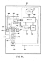
図1は、本発明の実施形態による反射モード装置の例を示す。図1は、光源、検出器、光源と検出器の間のいくつかの部品を示す。光源105からの光はビームスプリッタ110を通過し、干渉計ミラー115によってスペクトルフィルター120へ反射される。スペクトルフィルター120からの光は、集束及びビーム操縦光学系125及び130によってサンプルホルダ150の底部へ集束する。次いで、光は1回又は複数回の通過で各サンプルと相互作用し、次いでサンプルホルダ150の外へ反射され、光学系135によって赤外線カメラ140へ集束される。図1に示したこのシステムの実施形態は、(1)赤外線源、(2)放射を変調するデバイス、(3)サンプルホルダ、(4)赤外検出器、(5)操舵光学系、及び(6)スペクトルデータを収集、処理して提示するコンピュータの6つの構成要素を含む。
FIG. 1 shows an example of a reflection mode device according to an embodiment of the present invention. FIG. 1 shows a light source, a detector, and some components between the light source and the detector. Light from the
図2は、本発明の実施形態による透過モードの装置の例を示す。ここで、光源205からの放射は、ビームスプリッタ210を通過し、干渉計ミラー215によってスペクトルフィルター220へ反射される。スペクトルフィルター220からの光は集束光学系225によってサンプルホルダ230の底部へ集束し、ホルダ230内のサンプルアレイの各要素は同時に照射される。放射はサンプルを通過し、次いで光学系235によって集束して赤外線カメラ240へ入射する。
FIG. 2 shows an example of a device in transmissive mode according to an embodiment of the present invention. Here, the radiation from the
透過測定は、光源からの光をサンプル及び検出器を通過させることによって行われ、一般に反射測定用に用いられるものとは異なるサンプルホルダが必要である。溶液ベースの赤外透過測定は、一般に短い経路長の透過セル又は貫流セルを必要とする。両方の構成において、サンプルを通る光路長は水性溶液において長さ約10〜50ミクロンなどの短い距離に制限される。サンプルは、サンプルを拘束し、サンプルを通じて経路長を固定するように設計された、薄いガスケット(Teflon)によって分離された2個の赤外透過窓の間に挟むことができる。類似のサンプルホルダが存在し、サンプルは、光の出入りが可能な赤外線に対して透過の側壁を有する管を通って流れる。どちらの構成も複数のサンプルから同時に赤外吸収スペクトルを得ることは不可能である。したがって、並列の複数の透過測定の問題は、(i)赤外ビーム中のすべてのサンプルの分離、(ii)必要な短い経路長の制御、(iii)溶媒蒸発の低減が必要なことであると言える。 Transmission measurements are performed by passing light from the light source through the sample and detector, and generally require a different sample holder from that used for reflection measurements. Solution-based infrared transmission measurements generally require a short path length transmission or flow-through cell. In both configurations, the optical path length through the sample is limited to short distances such as about 10-50 microns in length in aqueous solutions. The sample can be sandwiched between two infrared transmission windows separated by a thin gasket (Teflon) designed to constrain the sample and fix the path length through the sample. There is a similar sample holder, and the sample flows through a tube with side walls that are transparent to the infrared where light can enter and exit. In either configuration, it is impossible to obtain an infrared absorption spectrum from a plurality of samples at the same time. Thus, the problem of multiple transmission measurements in parallel is that (i) separation of all samples in the infrared beam, (ii) control of the required short path length, and (iii) reduction of solvent evaporation are required. It can be said.
これらの問題は、図3に例示したように並列のサンプルホルダの発見によって首尾よく対処された。このサンプルホルダは、これらの問題を軽減するいくつかの特徴を有する。第1に、ホルダは光がサンプルを通過することのできる赤外線透過性の領域を含む。これらの赤外線透過性のサンプリング領域はホルダ全体を赤外線透過性の媒体から構成することによって、又は一連の赤外線透過性の窓を不透過な母材に一体化することによって作製することができる。第2に、サンプルホルダは、図3に見られるように特定のサンプル注入口を含む。各サンプルの位置は、反応物、溶媒等の混合を可能にするいくつかのサンプル注入口を有することができる。最終的に、サンプル注入口はマイクロチャンネルによって赤外サンプリング領域に接続しており、口からサンプリング領域へ毛細管作用によってサンプルが動くことを可能にする。毛細管によって供給される短い通路長のサンプリング領域は、サンプルを通るビーム通路の制限及び溶媒蒸発を低減するのに必要な絶縁に適するように修正することができる。 These problems were successfully addressed by the discovery of parallel sample holders as illustrated in FIG. This sample holder has several features that alleviate these problems. First, the holder includes an infrared transparent region that allows light to pass through the sample. These infrared transmissive sampling regions can be made by constructing the entire holder from an infrared transmissive medium or by integrating a series of infrared transmissive windows into an impermeable matrix. Second, the sample holder includes a specific sample inlet as seen in FIG. Each sample location can have several sample inlets that allow mixing of reactants, solvents, and the like. Finally, the sample inlet is connected to the infrared sampling region by a microchannel, allowing the sample to move from the mouth to the sampling region by capillary action. The short path length sampling area provided by the capillary can be modified to suit the beam path restriction through the sample and the insulation necessary to reduce solvent evaporation.
さらに具体的に、図3aは赤外線透過性の材料から作られた3個のサンプリングユニットを有するサンプルホルダ300の側面図を示す。最も左のユニットに見ることができるように、サンプル注入/取り出し口310はサンプル又はサンプル流の添加又は除去のために使用され、サンプル又はサンプル流は毛細管微小チャンネル320を通ってサンプリング領域330へ流れ、次いでサンプル注入/取り出し口340を出る。
More specifically, FIG. 3a shows a side view of a
図3bは本発明の実施形態による、不透過な母材領域360をさらに含むサンプルホルダ350を示す。
FIG. 3b shows a
これらのサンプルホルダ、及び、以下に説明する図4A乃至20に示されたサンプルホルダの赤外線透過性の領域は、ハロゲン化アルカリ塩(KBr又はNaCl)、CaF2、BaF2、ZnSe、 Ge、Si、シリコンベースの材料(例えば二酸化ケイ素、その他)ポリシリコン、半導体材料、結晶シリコン、ガラス、サファイヤ、クォーツ、薄いポリエチレン、ポリテトラフルオロエチレン(PTFE)、又はAMT赤外線及びKRS-5などの特殊な赤外材料など1種又は複数の赤外線透過性の材料とすることができる。Si 及びGeなどの材料を使用することによって、サンプルアレイ全体をリソグラフィー及び標準的な半導体加工技術を用いて微小加工することができる。不透過な母材はプラスチック、ガラス、ワックス、ポリマー、エラストマー等などの低コスト材料から作ることができる。一実施例において、ここで利用される半導体基板は、伝導帯を価電子帯から切り離す、ゼロではないエネルギーギャップを有する材料からなる基板を用いる。この種の典型的な材料は、例えば、Si、Ge、GaAs、ZnSe及びZnSを含む。 These sample holders and the infrared transparent regions of the sample holders shown in FIGS. 4A to 20 described below are alkali halide salts (KBr or NaCl), CaF 2 , BaF 2 , ZnSe, Ge, Si , Silicon based materials (eg silicon dioxide, etc.) polysilicon, semiconductor materials, crystalline silicon, glass, sapphire, quartz, thin polyethylene, polytetrafluoroethylene (PTFE), or special reds such as AMT infrared and KRS-5 One or more infrared transparent materials such as an external material can be used. By using materials such as Si and Ge, the entire sample array can be microfabricated using lithography and standard semiconductor processing techniques. The impermeable matrix can be made from low cost materials such as plastic, glass, wax, polymer, elastomer and the like. In one embodiment, the semiconductor substrate utilized herein is a substrate made of a material having a non-zero energy gap that separates the conduction band from the valence band. Typical materials of this type include, for example, Si, Ge, GaAs, ZnSe and ZnS.
意図している用途の大部分は、5〜16.5ミクロン(1ミクロン=10-6メートル)の波長のスペクトル情報を蓄積する必要がある。赤外源は可視から遠赤外の広い波長範囲にわたる放射を放出し、本発明の実施形態は様々な波長を使用する。望ましいスペクトル窓の外側の赤外波長はサンプルの加熱によって測定に悪い影響を与えることがある。すなわち、制御されない加熱は背景(基準線信号)の移動を招き、測定の雑音対信号比を低下させる。したがって、放射源からの赤外線を対象帯域幅に制限するために、スペクトルフィルターを含み、放射源から発生するが測定には必要のない他の放射を遮断することが好ましい。 Most of the intended applications need to store spectral information at wavelengths between 5 and 16.5 microns (1 micron = 10 −6 meters). Infrared sources emit radiation over a wide wavelength range from the visible to the far infrared, and embodiments of the present invention use a variety of wavelengths. Infrared wavelengths outside the desired spectral window can adversely affect the measurement by heating the sample. That is, uncontrolled heating causes movement of the background (reference line signal) and reduces the noise-to-signal ratio of the measurement. Therefore, in order to limit the infrared radiation from the radiation source to the target bandwidth, it is preferable to include a spectral filter to block other radiation generated from the radiation source but not required for the measurement.
それらの遮断は、小さな面積のサンプルのために光の強度を増加する(高密度出力の用途)とき特に価値がある。赤外フィルターは、赤外線透過性の基板上の特殊な材料(金属及び半導体)薄膜の堆積によって作製することができる。一般的な概論は、http: //www.ocli.com/pdf_files/products/gen_info_infrared_filters.pdf又は O.S.Heavens Optical Properties of Thin Solid Films、1991、Dover Press、New Yorkの多くの光学情報源に見出すことができる。 These blockages are particularly valuable when increasing the light intensity for small area samples (high density output applications). Infrared filters can be made by depositing a special material (metal and semiconductor) thin film on an infrared transparent substrate. A general overview can be found at http://www.ocli.com/pdf_files/products/gen_info_infrared_filters.pdf or OSHeavens Optical Properties of Thin Solid Films, 1991, Dover Press, New York. it can.
フーリエ変換と組み合わせた変調は、信号と分析の時間を向上させるのに特に強力である。光源からの光は干渉計で変調することが好ましい。好ましい干渉計は Michelson干渉計である。多数の他の干渉計設計が存在し、適している。1つ又は複数の実施形態において、原理的に、光路差を生成する任意の干渉計が役に立つであろう。 Modulation combined with Fourier transform is particularly powerful in improving signal and analysis time. The light from the light source is preferably modulated with an interferometer. A preferred interferometer is a Michelson interferometer. Many other interferometer designs exist and are suitable. In principle, any interferometer that produces an optical path difference will be useful in one or more embodiments.
多くの研究所ベースの中間赤外像形成分光計は、放射がサンプルと相互作用する前に、マイケルソン(Michelson)干渉計を使用して赤外線を変調する。しばしば Michelson干渉計は市販のFT-赤外線分光計において、そのシステムの「光源」として使用される。Michelson干渉計は、2個の分割光源の構成要素間の光路差を発生させるために可動ミラーシステムを使用する。2ビーム干渉計のスペクトル解像度は干渉計中の全体的な光路差及び検出器が読み取られる光路差の数(測定されるミラーの位置の数)に基づく。各光路差からのデータは数学的(例えばフーリエ)変換アルゴリズム及びコンピュータを援用して吸収スペクトルに変換される。 Many laboratory-based mid-infrared imaging spectrometers use a Michelson interferometer to modulate the infrared radiation before the radiation interacts with the sample. Often Michelson interferometers are used as “light sources” for the systems in commercial FT-IR spectrometers. The Michelson interferometer uses a movable mirror system to generate an optical path difference between the components of two split light sources. The spectral resolution of a two-beam interferometer is based on the overall optical path difference in the interferometer and the number of optical path differences at which the detector is read (number of mirror positions measured). Data from each optical path difference is converted to an absorption spectrum with the aid of a mathematical (eg, Fourier) transformation algorithm and a computer.
2ビームシステムは非常に広い帯域幅(25,000〜13cm-1)、及び非常に高い解像度(〜0.005cm-1) が可能であり、本発明の実施形態に有用であるので特別に説明する。測定される事象の動力学がミラーの速度と同じタイムスケールにあるとき、1個又は両方のミラーを動かす必要性は、時間依存分析を複雑にする。言い換えれば、データはミラー経路の1つの長さを掃引するのに必要な時間で平均化され、速度と解像度は逆の相関がある。或る2ビーム干渉計はステップ-スキャン形態を用い、干渉計は段階的に固定光路差に進み、その経路長の周辺で少量の走査(小さなミラーの動き)を行う。 The two-beam system is specifically described as it is capable of very wide bandwidth (25,000 to 13 cm −1 ) and very high resolution (˜0.005 cm −1 ) and is useful for embodiments of the present invention. The need to move one or both mirrors complicates time-dependent analysis when the measured event dynamics are on the same time scale as the mirror speed. In other words, the data is averaged over the time required to sweep one length of the mirror path, and speed and resolution are inversely related. Some two-beam interferometers use a step-scan configuration, where the interferometer advances in steps to a fixed optical path difference and performs a small amount of scanning (small mirror movement) around its path length.
アレイからデータを得るのに必要な時間が増加するので、像形成システムへの影響は大きい。アレイ速度は一般にサイズと共に大きくなり、より小さなアレイはより速く、単一ピクセル検出器(FT-赤外線分光計に見られる)は一般にMHzの周波数で動作する。典型的な64×64ピクセルのHg-Cd-Teアレイは 3000Hzの最大フレーム速度を有し、特別のアレイは〜1KHzで動作が可能である。像は各光路差(ミラー位置)で取得しなければならず、スペクトル解像度は測定される異なるミラー位置の数に依存するので、より高い解像度は像形成の意味でより長い時間にも解釈される。 The impact on the imaging system is significant because the time required to obtain data from the array increases. Array speed generally increases with size, smaller arrays are faster, and single pixel detectors (as found in FT-infrared spectrometers) generally operate at frequencies of MHz. A typical 64x64 pixel Hg-Cd-Te array has a maximum frame rate of 3000Hz, and a special array can operate at ~ 1KHz. Images must be acquired at each optical path difference (mirror position), and the spectral resolution depends on the number of different mirror positions measured, so higher resolution is interpreted in longer time in the sense of imaging .
速度の問題をさらに複雑にするのは、多くの化学的及び生物学的反応が多数のスペクトルを必要とし、データ処理の前に雑音低減のために平均化しなければならないことである。典型的なタンパク質実験は、例えば、平滑化、誘導、曲線当てはめ等などの1種又は複数のアルゴリズムで数学的に処理するために、100個又はそれを超えるスペクトルの組み合わせを必要とするであろう。本発明の実施形態はアレイ中の各サンプルから迅速な複数のスペクトルを提供し、システムの性能を向上させ、良好なサンプルスループットを提供する。 To further complicate the speed problem, many chemical and biological reactions require a large number of spectra and must be averaged for noise reduction prior to data processing. A typical protein experiment will require a combination of 100 or more spectra for mathematical processing with one or more algorithms such as smoothing, derivation, curve fitting, etc. . Embodiments of the present invention provide rapid multiple spectra from each sample in the array, improving system performance and providing good sample throughput.
水性溶液中の赤外測定を行うとき、雑音に最も大きく寄与するものの1つは、背景(基準線)の移動である。この問題は背景(基準線)測定を行い、次いでその測定値を後続のスペクトルの参照に使用することによって対処される。多くの場合、保存された基準線スペクトルは後続のスペクトルから差し引かれる。典型的に基準線は温度の変化、又は湿度への変化、二酸化炭素含有量等などの大気条件の変化によって変化するであろう。これらの変化は不十分な減算、又は背景効果の過剰補償として現れる。移動の問題は、希釈された分子濃度の測定で深刻であり、基準線の雑音が溶液中の分子からの望ましい信号を凌駕する。 When making infrared measurements in aqueous solutions, one of the biggest contributors to noise is the movement of the background (reference line). This problem is addressed by taking a background (baseline) measurement and then using that measurement for subsequent spectral reference. In many cases, the stored baseline spectrum is subtracted from subsequent spectra. Typically, the baseline will change due to changes in temperature, or changes in atmospheric conditions such as changes to humidity, carbon dioxide content, and the like. These changes appear as insufficient subtraction or overcompensation of background effects. The problem of migration is severe in measuring diluted molecule concentrations, and baseline noise exceeds the desired signal from molecules in solution.
これらの目的のための並列赤外分光計は、5〜17ミクロンの波長範囲の中間赤外線に敏感な検出器を持たなければならない。これらの検出器は、Hg-Cd- Te、DTGS、サーモパイルなどの材料、量子ウェル赤外光検出器(QWIP)、ならびに多くの冷却及び非冷却ボロメーターを含む。像形成又は並列分光計において、これらの検出器は直線(1×128、1×256等)又は矩形アレイ(64×64、128×128、4×256等)のいずれかで見られる。検出器及び読み取り電子機器は赤外線カメラの構成要素を形成する。カメラは、標準的なパーソナルコンピュータ上の数学的変換アルゴリズムを用いて入って来る放射をスペクトル像に変換する。 Parallel infrared spectrometers for these purposes must have detectors that are sensitive to mid-infrared in the 5-17 micron wavelength range. These detectors include materials such as Hg-Cd-Te, DTGS, thermopile, quantum well infrared photodetectors (QWIP), and many cooled and uncooled bolometers. In imaging or parallel spectrometers, these detectors can be seen either as straight lines (1 × 128, 1 × 256, etc.) or rectangular arrays (64 × 64, 128 × 128, 4 × 256, etc.). The detector and reading electronics form the components of an infrared camera. The camera converts incoming radiation into a spectral image using a mathematical conversion algorithm on a standard personal computer.
多数の化学的及び生物学的反応が、水性又は中間赤外線を良く吸収する有機溶媒中で起きる。例えば、中間赤外スペクトル領域の強い吸収は、一般に水性溶液の中で光路長を5〜10ミクロンに制限する。従来の一度に一回の分光計はこれらの環境でスペクトルを得るために典型的に3つの手法を用いる。それらは、短い経路長あるいは貫通セル、全内部反射、及び溶媒蒸発を含む。各手法は赤外線透過性のサンプルホルダ、又は少なくとも透過なホルダの領域の必要性によって制約を受ける。本明細書に述べる多くの実施形態はこの問題を(従来技術に比べて)サンプルサイズの縮小化、及び多数のサンプルの同時アッセイによって対処する。 A number of chemical and biological reactions occur in aqueous or organic solvents that absorb mid-infrared well. For example, strong absorption in the mid-infrared spectral region generally limits the optical path length to 5-10 microns in aqueous solutions. Conventional once-at-a-time spectrometers typically use three techniques to obtain spectra in these environments. They include short path lengths or through cells, total internal reflection, and solvent evaporation. Each approach is constrained by the need for an infrared transparent sample holder, or at least a transparent holder area. Many embodiments described herein address this problem by reducing sample size (as compared to the prior art) and simultaneous assaying of multiple samples.
本発明の実施形態は、光と対象分子に見出される化学結合電子との相互作用によって得られる診断信号を提供する。診断信号は検出された光信号に相当する電子衝撃から生成する。したがって、良好な雑音(不規則な電子的背景信号)対信号比は、測定時間が短くなると処理された光の量(及び光から得られる電気信号)がより小さくなるので、迅速な測定値を得るために重要である。赤外光は、望ましいスペクトル処理が一般に4000〜400cm-1(2.5〜25ミクロン)で画定される光スペクトルの中間赤外領域で分子の基本振動共鳴を伴う、多くの実施形態に用いられる。生物学的化合物の大部分は1800〜600cm-1(5.5〜16.7ミクロン)に制限される。 Embodiments of the present invention provide a diagnostic signal obtained by the interaction of light and chemically bonded electrons found in the molecule of interest. The diagnostic signal is generated from an electron impact corresponding to the detected optical signal. Therefore, a good noise (irregular electronic background signal) to signal ratio is a quick measurement because the amount of processed light (and the electrical signal derived from the light) becomes smaller as the measurement time is shortened. Is important to get. Infrared light is used in many embodiments with fundamental vibrational resonances of molecules in the mid-infrared region of the light spectrum where the desired spectral processing is generally defined by 4000-400 cm −1 (2.5-25 microns). The majority of biological compounds are limited to 1800-600 cm -1 (5.5-16.7 microns).
赤外領域のプローブ光を発生するためには、「グローバー(glowbar)」(SiCなどの熱い材料)などの黒体放射源、サンプル又は場の固有の熱放射、又は太陽赤外線から典型的に使用される。好ましい光源は、単一グローバー(シリコンカーバイド棒)、Nernst発光体(希土類酸化物の円筒)、又は白熱線を含む。光源は、典型的に出力約50〜100W、及びビーム直径約4cm、又はビーム出力密度約4W/cm2を有することができる。この出力密度は光学系を小さなサンプルに焦点を合わせることによって高めることができ、アパーチャーを光源とサンプルの間に置くときに低下させることができる。この出力密度は、ビーム通路中の単一サンプル、又はビームが特定の点に集束することのできる小さな面積のサンプルを含む従来の赤外実験には許容される。数百個の小さなサンプルが同時に測定されるときに存在する大面積のサンプリング環境において、有効面積を拡大するためにビームを広げることは、サンプルの各位置での出力密度を低下させる。したがって、より大きなサンプルの拡大した面積に有利な出力密度を維持するために、赤外光源の出力を増加することが望ましい。 Typically used from black body radiation sources such as “glowbars” (hot materials such as SiC), sample or field intrinsic thermal radiation, or solar infrared to generate infrared probe light Is done. Preferred light sources include single glow bars (silicon carbide rods), Nernst emitters (rare earth oxide cylinders), or incandescent rays. The light source typically can have a power of about 50-100 W and a beam diameter of about 4 cm, or a beam power density of about 4 W / cm 2 . This power density can be increased by focusing the optical system on a small sample and can be reduced when the aperture is placed between the light source and the sample. This power density is acceptable for conventional infrared experiments involving a single sample in the beam path or a small area sample where the beam can be focused to a specific point. In a large sampling environment that exists when hundreds of small samples are measured simultaneously, expanding the beam to expand the effective area reduces the power density at each location of the sample. Therefore, it is desirable to increase the output of the infrared light source in order to maintain an advantageous power density for the enlarged area of the larger sample.
一実施形態において、赤外測定に使用されるものなどの回転ミラー干渉計は、より短い波長の光に必要なミラー回転速度を高めるために修正される。光変調技術の将来の進歩は、適切な変調を発生させるより便利な代わりの方法を提供するであろうが、本発明の実施形態に意図されている。 In one embodiment, rotating mirror interferometers such as those used for infrared measurements are modified to increase the mirror rotation speed required for shorter wavelengths of light. Future advances in light modulation technology will provide a more convenient alternative method of generating proper modulation, but are contemplated by embodiments of the present invention.
本明細書に述べる赤外技術と組み合わせて、蛍光、リン光、時分割(time resolved)蛍光、及び/又は化学蛍光を用いることができる。さらに分子及び代謝情報を明らかにするために、薬剤発見方法はそれらの追加の情報を有利に利用することができる。追加の情報は、サンプル中の試験化合物の効果が非常に複雑で、複数の化学的相互作用が試験される必要のある生物化学及び細胞研究に特に役に立つ。例えば、細胞はルシフェリン及びルシフェラーゼを現すように遺伝子的に加工され、生物化学的経路から光を発生し、新しい先導的な薬剤を試験する複数のサンプル・ウェルのプローブとして使用することができる。試験化合物からの効果は可視光信号として検出することができる。赤外反射及び可視光信号の両方を同時に監視することによって、試験化合物の細胞表面への化学的結合を監視することができ、生物化学的加工の時間及び効果を監視することができる。それらの一実施形態において、プリズムデバイスは赤外反射測定のサンプルアレイの下に用いることができ、可視光像形成検出器はサンプルアレイの上に置いてアレイから得られる光の位置と強度を監視することができる。検出された可視光信号及び反射分光信号は処理され比較されて、各サンプルに属する情報を発生する。 Fluorescence, phosphorescence, time resolved fluorescence, and / or chemical fluorescence can be used in combination with the infrared techniques described herein. In order to further reveal molecular and metabolic information, drug discovery methods can advantageously utilize these additional information. The additional information is particularly useful for biochemical and cellular studies where the effect of the test compound in the sample is very complex and multiple chemical interactions need to be tested. For example, cells can be genetically engineered to reveal luciferin and luciferase, generate light from biochemical pathways, and be used as multiple sample well probes to test new leading agents. The effect from the test compound can be detected as a visible light signal. By simultaneously monitoring both infrared reflection and visible light signals, the chemical binding of the test compound to the cell surface can be monitored, and the time and effect of biochemical processing can be monitored. In one such embodiment, the prism device can be used under an infrared reflectance measurement sample array, and a visible light imaging detector is placed over the sample array to monitor the position and intensity of light obtained from the array. can do. The detected visible light signal and the reflected spectral signal are processed and compared to generate information belonging to each sample.
図4Aから図20は、例えば赤外線分光法等の振動分光法を用い、複数の化学/生物サンプルを分析する方法及び装置の各種実施形態を示す。本方法及び装置が、例えば生物学及び化学において利用されているあらゆる適当な種類及び/又は数の分子のような、あらゆる適切なタイプの生物サンプルを分析することができ、検討することができることが理解されるべきである。さらに、各生体サンプルがサンプル成分(例えば、一つ以上の薬、抗体、水、タンパク質、生体分子、その他)のいかなる適当な数(例えば複数)も含むことができることが理解されるべきである。加えて、分析されるサンプルは、物理的状態(例えば液体、半流動体、半固体、固体、粉等)のいかなる適当な種類にあってもよい。実施例において、シリコンチップ/ウエハの活性表面上の毛細管で例示される複数の凹部は、例えば、分析されるサンプルで各々満たされる。次に、等電点分離法は、サンプルの中に含まれる異なる化学/生物学的成分を分離するために利用される。従って、電界が毛細管に印加され、そして、pH勾配が毛細管に沿って発生する。従って、サンプルの中の異なる分子は、それらの実効電荷がゼロである毛細管に沿って、異なる位置へ移動する。サンプルを通過した赤外線光は、赤外線カメラによって検出され、赤外線カメラは検出データをコンピュータに送信し、コンピュータは、フーリエ変換を実行することにより赤外線吸収スペクトルを生成する。特定の生物/化学成分(例えばタンパク質、遺伝物質、タンパク相互作用反応生成物、その他)が異なる波長で特定の赤外線吸収を生成するので、赤外線吸収スペクトルは何の成分がサンプルの中に存在するかについて判定するための試験を行うことができる。 FIGS. 4A-20 show various embodiments of methods and apparatus for analyzing multiple chemical / biological samples using vibrational spectroscopy, such as infrared spectroscopy. The method and apparatus can analyze and review any suitable type of biological sample, such as any suitable type and / or number of molecules utilized in biology and chemistry, for example. Should be understood. Furthermore, it should be understood that each biological sample can include any suitable number (eg, multiple) of sample components (eg, one or more drugs, antibodies, water, proteins, biomolecules, etc.). In addition, the sample to be analyzed may be in any suitable type of physical state (eg, liquid, semi-fluid, semi-solid, solid, powder, etc.). In an embodiment, a plurality of recesses, exemplified by capillaries on the active surface of a silicon chip / wafer, are each filled with a sample to be analyzed, for example. The isoelectric point separation method is then utilized to separate the different chemical / biological components contained in the sample. Thus, an electric field is applied to the capillary and a pH gradient is generated along the capillary. Thus, the different molecules in the sample move to different positions along the capillary where their net charge is zero. Infrared light that has passed through the sample is detected by an infrared camera, which transmits detection data to a computer, which generates an infrared absorption spectrum by performing a Fourier transform. Because certain biological / chemical components (eg proteins, genetic material, protein interaction reaction products, etc.) produce specific infrared absorptions at different wavelengths, the infrared absorption spectrum shows what components are present in the sample Tests can be performed to determine
図4Aは、本発明の一実施例に係る複数のサンプルを分析するシステム400を表す。図4Aのシステム400が理解の容易さのために単純化されたことが理解されるべきである。実施例において、複数のサンプルを分析するシステム400は、分析されるもう一つのサンプルを含むサンプルホルダ462による赤外線光を照射する光源480を含む。サンプルは、赤外線分光法によって分析されることができるいかなる適当なサンプル(例えば生物学的製剤、化学物質、その他)でもあってもよいことが理解されるべきである。サンプルを通じて照射された赤外線光は、赤外線カメラ448によって検出されることができる。カメラ448によって受光される光信号を分析することによって、赤外線吸収スペクトルを含む赤外線吸収マップは、例えば、サンプルホルダ462のサンプルの成分を判定して/特徴づけるために生成されることができる。赤外線吸収マップは、サンプルの赤外線光吸収を示すことができる、図的及び/又は数式的表現のいかなる適当な種類でもあってもよい。実施例において、赤外線吸収データは、サンプルを通じて送られる赤外光の検出に基づく少なくとも一つのデータ点として示されることができる。赤外線吸収マップの例示的実施形態は、図11C、12A及び12bに示される。
FIG. 4A depicts a
図4Bは、本発明の一実施例に係る複数のサンプルを分析するシステム400のより詳細なブロック図を示す。実施例において、複数サンプル分析システム400は、干渉計500へ光を照射し、赤外光によって生成されたあらゆる波長の同相波及び位相外れ波の赤外光を生成するための赤外線源504を含む。実施例において、図5Bに関して更に詳細に述べられるように、光源480は干渉計500及び赤外線源504を含む。HeNeレーザは、干渉計500の変調を観測する時計として利用されることができる。同相及び位相外れ赤外線光波は、サンプルホルダ462のサンプルを通じて伝達されることができる。実施例において、サンプルホルダ462は、ウエハ(例えばチップ)及び/又はウエハホルダを含むことができる。読取りヘッド458は上方向(システム400の構成次第では下方向)移動することができ、そして、サンプルホルダ462のサンプルを通じて発信された赤外線光透過を受光するために、読取りヘッド458はサンプルホルダ462に付属される。カメラ448は、読取りヘッドから光信号を受光することができ、サンプルの赤外線吸収を組み込む電気的信号を生成する。電気的信号はコンピュータ412に送信されることで、サンプルの各々の成分についての赤外線吸収スペクトル生成のためのフーリエ変換が行われる。
FIG. 4B shows a more detailed block diagram of a
図5Aは、本発明の一実施例に係る複数のサンプルを分析するシステム400の詳細なブロック図を示す。実施例において、複数サンプル分析システム400は、光信号を受信することができるカメラ448を含む。上記の通り、カメラ448は分析される複数のサンプルを通じて照射される赤外光を検出することができる装置のいかなる適当な種類でもあってもよいことが理解されるべきである。カメラ448は赤外線検出器(例えば焦点面アレイ488)(FRA)を含むことができ、カメラ448は赤外線光を受光して、記録するためにデュワー450の中に組み込まれる。実施例において、カメラ448は、約5〜約10ミクロンの間で光波長を検出するように構成されることができる。ある特定の実施例では、128x128ピクセルHgCdTe焦点配列(FRA)カメラを利用することができる。例えばスキャン光学、回転鏡、可動鏡を有する単一検出器、その他等、いかなる適当な赤外線検出/走査する装置が、赤外線光を受光し、記録することができる装置において利用されることが理解されるべきである。
FIG. 5A shows a detailed block diagram of a
デュワー450は、赤外線検出環境の温度を制御することができる被覆であってもよい。実施例において、デュワー450は、試験されるべきサンプルが通過した赤外線信号を受光することができる光学系460を囲む。温度は、被覆の温度制御流体(例えば窒素)の適用によって管理されることができる。FRA488は、次に光学系460から赤外線光を検出することができて、この検出からデータを記録することができる。
The
複数サンプル分析システム400は、書込みヘッド456及び読取りヘッド458を含むこともできる。更に以下でも説明されるように、書込みヘッド456はソースプレートのウェルからサンプルを取り去ることができて、赤外線分光法のためのウエハの凹部(例えば毛細管)にサンプルを投入することができる。実施例において、書込みヘッド456は、ソースプレート及びウエハ上を垂直に移動するように構成される。ソースプレート及びウエハと共に用いられる読取りヘッド458及び書込みヘッド456については図6にて更に詳細に説明する。
The multiple
テストを開始する際に、テストすべきサンプルを含むソースプレートは書き込みヘッド456の下に移動する。ソースプレートに関しては、図15で更に詳細に説明する。書込みヘッド456は、ソースプレートからサンプルを取り除くために、ソースプレート上まで下降することができる。書込みヘッド456は、ソースプレートを離れて移動する。次に、書込みヘッド456がソースプレートからサンプルホルダ462にサンプルを投入する場合に、サンプルホルダ462は、書込みヘッド456の下に移動することができる。
When starting the test, the source plate containing the sample to be tested moves under the
サンプルテストの一実施例において、サンプルホルダ462は、分析環境が実質的に恒常的な状態に保たれるように、制御された窒素ガス雰囲気を有するシステム400の範囲内の領域である活性領域454に設置されることができる。サンプルホルダ462は、書込みヘッド456か読取りヘッド458の下にサンプルホルダを動かす可動テーブルに設置されることができる。他の実施例においては、カメラ448、読取りヘッド458及び/又は書込みヘッド456はサンプルホルダ462の下に位置する所で利用されることができることが理解されるべきである。また、書込みヘッドがソースプレートからサンプルを取り出すことができて、サンプルホルダ462にサンプルを投入することができるように、可動テーブル(図6を参照して詳述)は書込みヘッド456の下で分析される複数のサンプルを有するソースプレートを動かすこともできる。サンプルがサンプルホルダ462に投入された後、サンプルホルダ462は読取りヘッド458の下に移動することができる。
In one example of sample testing, the
実施例において、書込みヘッド456がサンプルをサンプルホルダ462に載せたあと、サンプルホルダ462は読取りヘッド458の下に移動することができる。読取りヘッド458は、分析されるサンプルを含むウエハ上に垂直に移動するように構成される。次に、読取りヘッド458は、サンプルホルダ462上まで下降することができる。実施例において、読取りヘッド458はサンプルホルダ462に付属し、そして、光源480はサンプルホルダ462を通じて赤外線光を照射することができる。従って、実施例において、読出しヘッド458及び書込みヘッド456は垂直にそれぞれ移動可能でもよい。サンプルホルダ462が読出しヘッド458及び書込みヘッド456のいずれの下に移動するときに、読出しヘッド458及び書込みヘッド456のいずれもサンプルホルダ462上及び/又はサンプルホルダ462へ下降することができる。
In an embodiment, the
読取りヘッド458は、ウエハに定義される各々の毛細管の2つの端に電荷を印加することができ、複数のプローブ(例えば電圧ピン)を含むこともできる。従って、読取りヘッド458は電圧アプリケータであってもよい。電荷の印加は、生体分子を分離するため、等電点分離法を容易にすることができる。読取りヘッド458は、赤外線光を透過するウインドウを有することもできる。これにより、サンプルホルダ462の下から発信された赤外線光が、カメラ448のFPA488によって検出されるために、読取りヘッド458のウインドウを通じて発信されることができる。読取りヘッド458及びサンプルホルダ462は、後述する図を参照しつつ、更に詳細に説明する。
Read
実施例において、赤外光がサンプルホルダ462の範囲内で含まれるサンプルに当てられることができるように、光源480は複数のサンプルを分析するシステムの中に設置されることができる。図5Bを参照しつつ更に詳細に説明されるように、光源480は干渉計を含むことができる。一実施例において、サンプルホルダ462が複数の凹部を有する基板であってもよい。ここで、サンプルホルダ462は、例えば、凹部の各々が分析されるサンプルを含むように構成される毛細管でもよい。他の実施形態では、サンプルホルダ462は、ウエハホルダに取り付けられるウエハを含むことができる。ウエハにおいて定義される凹部は、図9A乃至図9C及び図10Aを参照しつつ更に詳細に説明される。
In an embodiment, the
動作に関し、サンプルの中の生物学的成分は、成分の生物学的組成によって特定の波長/周波数の赤外線光を吸収することができる。実施例において、サンプルホルダ462を通じて発信された赤外線光は、カメラ448のFPA488によって検出される。赤外線光を透過するデュワー450の終端に位置するウインドウにより、赤外線光はFPA488によって検出されることができる。FPA488によって受光される光信号は、デュワー450の中で位置する電子回路452に発信されることができる。当業者ならば周知のように、デュワー450は、フレームレート、クロック・サイクル等を制御することによって焦点面アレイの管理に寄与する電子回路452を含むことができる。電子回路452は、コンピュータ412の範囲内でカメラ448及びフレームグラッバ444の間の通信を容易にすることもできる。従って、光信号は、デュワー450からフレームグラッバ444へ発信されることができて、メモリ446の中に格納されることができる。コンピュータ412の内部のメモリ446は、フレームグラッバ444からデータを受信し、格納することができるキャッシュ・メモリであってもよい。メモリ446(例えばキャッシュ・メモリ)の利用によって、赤外線分光処理を高いフレームレートで使用が可能になる。
In operation, a biological component in a sample can absorb infrared light of a specific wavelength / frequency depending on the biological composition of the component. In the embodiment, the infrared light transmitted through the
プロセッサ442は、サンプルを通じて照射された光信号を検出するための光源480及びカメラ448を管理するように構成されるプログラム440を実行する。カメラ448から受光される光信号は、サンプルホルダ462の範囲内でサンプルの成分を判定/特徴づけるために用いられることができる。
The
図5Bは、本発明の一実施例に係る干渉計500を示す。実施例において、干渉計500は、図5Aにて示す如く、光源480であってもよい。干渉計は、赤外線光を生成することができる赤外線源504を含むことができる。赤外線源504が赤外線スペクトルにおいて、ある光波ビーム生成するように構成されることが理解されるべきである。干渉計500の一つの簡略実施例において、赤外線光線514及び516は、赤外線源504によって生成される事が示される。二つの赤外線光線514及び516を有することが干渉計の仕組みを示す単なる実施例であることが理解されるべきである。従って、いかなる適当な光線の種類、及び/又は光線の数は、ここに用いられることができる。従って、赤外線光のいかなる適当な種類も、赤外線源によって生成されることができ、同相赤外線光波及び対応する位相外れ赤外線光波を生成するために、干渉計500によって処理されることができる。
FIG. 5B shows an
光線514は、鏡515にて反射され、分光器510へ進む。鏡515にて反射された光線514は、光線514-1として示される。一部の光線514-1は、分光器510にて反射して、光線514-2を形成する。光線514-1の他の部分は、分光器510の中で分離し反射せずに、分光器510を通じて移動して光線514-4を形成する。光線514-2は、鏡508の中で分離し反射して、サンプルに発信される光の一つである光線514-3を形成する。光線514-4は反射し、光線514-5を生成する。光線514-5は分光器510中で反射し、異なる距離のため、光線514-3と位相が一致せずに光線514-6を形成する。鏡508は、2つの分離した光線が進む異なる距離を生成するために、分光器510から異なる距離の場所へ移動することができる。異なる距離を進む分離した光線を有することによって、同位相である一つのビーム及び位相外れの光線を生成することができる。
The
光線516は鏡515で反射され、分光器510へ進む。鏡515で反射する光は、光線516-1として示される。一部の光線516-1は分光器510で反射し、光線516-2を形成する。光線516-1の他の部分は、分光器510の中で離れて反射せず、分光器510を通じて移動して光線516-4を形成する。光線516-2は鏡508で反射し、サンプルに発信される光の一つである光線516-3を形成する。上記のように、分光器510によって分割された光線が異なる距離を進むことができるように、鏡508は分光器510から異なる距離を移動するようにしてもよい。光線516-4は、光線516-5を生成する鏡512で反射する。光線516-5は分光器510で反射し、光線が進む異なる距離のため、光線516-3とは位相が一致しない光線516-6を形成する。このような方法で、干渉計は、位相外れの可能性がある赤外線の光波を有する赤外光を生成するように構成される。
The
光源480は、変調を干渉計に設定することができるレーザ501を含むことができる。いかなる適当な装置もレーザ501からの光を変調するために使用されることができることが理解されるべきである。例えば、同相及び位相外れ赤外線光波の進行距離を区別するために使用される可動鏡の位置を観測するモーターを有する符号器の如くである。レーザ501によって生成される光は、光線514及び516と同様にレーザ光線を分割することができる分光器510に発信されることができる。レーザ501が光線514及び516の移相を管理するための参照光として用いられることができるように、レーザ検出器518はレーザ501から光線を検出するように構成することができる。
The
図6は、本発明の一実施例に係る読取りヘッド458及び書込みヘッド456を示す。実施例において、ソースプレート530は、書込みヘッド456の下にソースプレート530をいかなる適当な方向にもおいてを移動する側方移動することができるテーブル532にあることができる。テーブル532がシステムの構成次第でいかなる適当な方向(垂直に、水平、その他)にもおいて移動するように構成することができることが理解されるべきである。実施例において、書込みヘッド456は、ソースプレート530の複数のウェルからサンプルを取り除くことができるピン534を含むように構成される。実施例において、3つ毎のウェルは、ウエハ550の単一の毛細管に対応することができる。書込みヘッド456は、ソースプレート530からサンプルを取り除き、サンプルホルダ462にサンプルを投入するために、例えば、ピンや管等を用いる適当な装置を利用することができることが理解されるべきである。実施例において、サンプルを取り除いて、サンプルを投入するためにピン534によって生成される際の書込みヘッド456は差圧を使用することができる。実施例において、流体の生物学的サンプルはピン534で定義される内側通路を通じて取り除かれることができ、生物学的サンプルはピン534において定義される内側通路からサンプルホルダ462に投入することができる。
FIG. 6 shows a
書込みヘッド456が例えば任意の適当な数の流体除去器具(例えばピン)を含むことができることが理解されるべきである。例えば、その数は1、20、50、100、その他がサンプルホルダ462に移動されることを要求されるサンプルの数による。実施例において、書込みヘッド456は、30本のピンを有することができる。ピン534がソースプレート530からのサンプルの除去し、かつ、ピンが知的な方法によって、サンプルをサンプルホルダに投入することを可能とする限りにおいて、いかなる適当な構成であってもよいということを認識されなければならない。実施例において、30個のピン書込みヘッドのピン構成は、3本の列及び10行のピンを有することができる。この種の構成において、ピンの各行は、図9、図10A及び図10Bに関して更に詳細に説明したように、10個の毛細管のサンプルホルダのうちの1つの毛細管に、流体を投入することができる。
It should be understood that the
読取りヘッド458はカメラに連結することができ、また、実施例において、読み取りヘッド458はサンプルホルダ462が読取りヘッド458の下の位置へ移動するときに、サンプルホルダ462に接続するために上下に移動可能とすることができる。読取りヘッド458は、サンプルを通じて発信された赤外線光が焦点面アレイ488によって検出されるようにウインドウ590を含むことができる。実施例において、赤外線光検出の条件が制御されることができるように、焦点面アレイ488はデュワー450に含まれることができる。
The read
図7Aは、本発明の一実施例に係る読取りヘッド458を示す。読取りヘッド458の本体は、いかなる適当な材料(例えばプラスチック)からも製造されることができる。加えて、読取りヘッド458がサンプルを通じて発信される赤外線光を効果的に受光することができる限り、読取りヘッド458はいかなる適当なサイズ及び形状であってもよい。実施例において、読取りヘッド458は高さ約3mmであって、サンプルホルダ462に付属するように構成される。読取りヘッド458は、サンプルが含まれる一部のウエハにサイズ及び形状において一致するウインドウ590を含むことができる。ウインドウ590は、赤外線光を実質的に透過するいかなる適当な材料でもあってもよい。読取りヘッド458は、複数の電圧ピン570及び572を含むこともできる。実施例において、電圧ピン570及び572の一組は、サンプルがウエハ内で保持可能な場所(例えば、毛細管)のあらゆる凹部に存在する。従って、サイズ及び凹部の形状に応じて、電圧ピン570及び572の位置及び数を変化させることができる。加えて、ウエハの凹部の配置に応じて、ウインドウ590のサイズ及び形状を異なるようにしてもよい。また、読取りヘッド458は、実質的にウインドウ590を囲み、図8Aに示すようにウエハホルダ560から読取りヘッド458を封止することができるガスケット604を含むことができる。一旦読取りヘッド458がウエハホルダ560に封止されると、毛細管の範囲内のサンプルは環境空気から封止され、これにより早熟な蒸発を実質的に減らしている。実施例において、毛細管が少量のサンプルを含むため、蒸発の減少は、サンプルテストが可能な時間を非常に増加させる。
FIG. 7A shows a
図7Bは、本発明の一実施例に係る読取りヘッド458の側面図を表す。実施例において、ピン570及び572は読取りヘッド458よりも引き出しているので、読取りヘッド458がサンプルホルダ462に取り付けられるときに、ピン570は特定の毛細管の一端に沈下する、そして、ピン572は特定の毛細管の他端に沈下する。任意の適当な数のピン570及び572が試験される毛細管の数に応じて読取りヘッドにあることができることが理解されるべきである。実施例において、サンプルホルダ上の各毛細管のために、ピン570及びピン572を用いることができる。
FIG. 7B depicts a side view of a
図7Cは、本発明の一実施例に係るウエハホルダ560に取り付けられるウエハ550の側面図を示す。実施例において、ウエハホルダ560は、ウエハ550の縁の部分周辺にウエハ550を保持するように構成されることができる。この種の構成において、ウエハホルダ560の中央の開口部は、赤外線光が開口部を通じて直接ウエハ550に発信されることを可能にする。ウエハホルダ560の一実施例は、図7Dを参照しつつ更に詳細に記載する。
FIG. 7C shows a side view of the
図7Dは、本発明の一実施例に係るウエハホルダ560の上面図を示す。ウエハ550が保持され、また、赤外線光はウエハホルダ560の開口部を通じて発信されることができる限り、ウエハホルダ560がいかなる適当なサイズ及び/又は形状であってもよいことが理解されるべきである。他の実施形態では、ウエハホルダ560が赤外線光を透過する材料から製造される限り、ウエハホルダ560は開口部を有する必要はない。一実施例において、ウエハホルダ560は、中央に矩形の穴を有することができ、これにより、光線は、ウエハ550の一面から入射され、ウエハ550の反対側から出射される。ウエハ550が安全に保持されることができる限り、ウエハホルダ560がいかなる適当な材料からも製造されることができる。
FIG. 7D shows a top view of a
図8Aは、本発明の一実施例に係るサンプルホルダ462に取り付けられる読取りヘッド458の横断面図を示す。実施例において、サンプルホルダ462は、ウエハホルダ560に取り付けられてその中に定義される凹部(例えば毛細管)を有するウエハ550を含む。ウエハ550は、図9A及び図9Bを参照しつつ更に詳細に説明する。ウエハ550は、ウエハホルダ560に取り付けられることができ、これにより、ウエハ550が赤外線光を透過する材料から作られるときに、赤外線光はウエハホルダ560の下から入射され、ウエハ550を通じて読取りヘッド458のウインドウ590に出射される。上記のように、赤外線透過材は、赤外線光線スペクトルの一部分又は全てを実質的に透過することができるいかなる適当な材料でもあってもよい。加えて、ウエハホルダ560の材料が赤外線光を実質的に透過する場合には、ウエハホルダ560は開口部を有する必要はない。
FIG. 8A shows a cross-sectional view of a
図8Bは、本発明の一実施例に係るウエハホルダ560と連結する読取りヘッド456の拡大図を示す。実施例において、読取りヘッド456は、ウエハホルダ560の表面に接続するガスケット604を含む。ガスケット604は、読取りヘッド456をウエハホルダ560から実質的に封止することができるいかなる適当な材料(例えばゴム、エラストマ等)から作製されることができることが理解されるべきである。読取りヘッド456は、ウエハ550を通じて送られる赤外線光線が入射することができるウインドウ590を含む。読取りヘッド456は、電圧ピン570及び572を含む。電圧ピン570及び572は、ウエハ550の毛細管に印加されることができ、これにより、等電点分離法が行われることができるように、電界は毛細管の長さ方向全体に渡って印加されることができる。
FIG. 8B shows an enlarged view of the read
図9Aは、本発明の一実施例に係る、サンプルが投入及び分析され、凹部を含むように構成されるウエハ550の上面図を示す。実施例において、ウエハ550は、テストされるサンプルを保持するためにウエハ550において定義される凹部(例えば毛細管)について、いかなる適当な数も及び/又は種類を有することができる。実施例において、凹部は、各々並列に間隔を置かれた複数の毛細管602-1〜602-10である。ウエハ550の表面に定義された凹部の他の例示的な形状は、図10C 乃至図10Eを用いて詳述する。実施例において、ウエハ550及び/又はウエハホルダ560は底の部分を形成することができ、そして、読取りヘッド458は接続構造の上部部分を形成することができる。従って、読取りヘッド458がウエハホルダ560に接続するときに、サンプルが所定期間外部環境にさらされないようにするため、毛細管は読取りヘッド458によって封止される。これは、サンプルの蒸発を減らすことができるという多大な効果がある。さらに別の実施形態では、ウエハ550は、サンプルの蒸発を減らすために、ウエハ550の範囲内の全面に定義される封じ込め空間を含むことができる。
FIG. 9A shows a top view of a
図9Bは、本発明の一実施例に係る他のウエハ550の上面図を示す。実施例において、ウエハ550は、図13にて更に詳細に述べられるように、複数の凹部(例えば毛細管)を含むことができる。図13で述べられるように、毛細管602は幅において毛細管602の中間の部分より各々大きい第1端部及び第2端部を有する。この種の構成において、サンプルが中間の部分に位置することができると共に、電圧プローブは第1端部及び第2端部に印加されることができる。
FIG. 9B shows a top view of another
図9Cは、本発明の一実施例に係る拡張した長さ毛細管602’を有するウエハ550’上面図を示す。本実施例において、生物学的サンプルの成分が伝播することができる長さは、実質的に重複する毛細管の部分に応じて延長される。実施例において、毛細管の602’は上記の通りにいかなる適当なサイズも有することができ、そして、好ましい実施例で、毛細管は幅約75ミクロンであってもよい。実施例において、望まれる移動距離にもよっては、毛細管の折り返し周期を増やすことは、成分が移動する必要がある距離を増加させることができる。このような実施例では、より大きいpH勾配は用いられることができ、また、より低い強度電界は利用されることができる。上記の通りの電界のいかなる適当な強度も利用されることができることが理解されるべきであるが、好ましい実施例で、約20V/cmの電界は利用されることができる。1つの例示的実施形態において、流体サンプルは、陽極及び陰極の間に毛細管の中間において投入されることができる。従って、毛細管の有効長を増加させることによって、移動に対する実効抵抗を増加することができ、そして、電界の低い強度は生物学的サンプルの成分を分離するために利用されることができる。 FIG. 9C shows a top view of a wafer 550 'having an extended length capillary 602' according to one embodiment of the present invention. In this example, the length that a biological sample component can propagate is extended depending on the portion of the capillary that substantially overlaps. In embodiments, the capillary 602 'can have any suitable size as described above, and in a preferred embodiment, the capillaries can be about 75 microns wide. In an embodiment, depending on the desired travel distance, increasing the capillary turn-back period can increase the distance that the component needs to travel. In such embodiments, larger pH gradients can be used, and lower strength electric fields can be utilized. It should be understood that any suitable strength of the electric field as described above can be utilized, but in a preferred embodiment, an electric field of about 20 V / cm can be utilized. In one exemplary embodiment, the fluid sample can be injected in the middle of the capillary between the anode and the cathode. Thus, by increasing the effective length of the capillary, the effective resistance to movement can be increased, and the low strength of the electric field can be exploited to separate the components of the biological sample.
図10aは、本発明の一実施例に係る毛細管602の側面図を示す。毛細管602は、サンプルの中の成分の分離が可能なように構成されることができる。実施例において、等電点分離法は、分子分離のために利用されることができる。他の実施形態では、電気泳動法は、分子分離のために用いられることができる。上述の等電点分離法の説明が利用されることができる1つの例示的な分離テクニックであることが理解されるべきであり、そして、分子分離技術の他の適当な種類が利用されることができる。
FIG. 10a shows a side view of a
一実施例において、毛細管602は、3つの部分を有する。第一の部分は、プローブ領域800、対のプローブ領域802、及びサンプルを収容領域804であってもよい。毛細管602のプローブ領域800は、酸性溶液を保持するための構成とすることができ、そして、対のプローブ領域802は、塩基性溶液(又はその逆、領域が負電荷若しくは陽電荷を有するによる)を有するように構成されることができると共に、サンプル収容領域804がサンプルを収容して、分析すべきサンプルを保持するように構成される。実施例において、pH勾配は、毛細管602の一端及び毛細管602の他端との間に生成される。加えて、電圧は電界を生成するために毛細管602の長さ全体に印加され、サンプルの分子の電気的性質に応じて、サンプルの異なる成分は毛細管の異なる領域へ移動する。実施例において、約20V〜約200Vの電圧が印加される。印加する他の方法として、毛細管に沿って生成されることができる電界が、約100V/cm及び300V/cmの間にあることができる。好ましい実施例において、約100Vの電圧が印加されることができる。
In one embodiment, the capillary 602 has three parts. The first portion may be a
従って、pH勾配及び電界を適用することによって、毛細管602の異なる領域は、異なる電気的及び酸性のレベルを有することができる。成分が例えば分析されて、タンパク質は、異なる電荷を有することができる。従って、異なる生物学的/化学成分の異なる等電特性のため、サンプルの各特定の成分は、毛細管602の異なる領域へ移動することができる。毛細管に沿った移動の間、成分は、pH勾配に沿って移動し、pH勾配に沿った成分の位置により、陽子を得る、若しくは、失う。一旦成分が充電されていない場所へ移動すると、成分の移動は止まることができる。この方法を用いて、分析されているサンプルの中の特定の成分(例えばタンパク質、タンパク相互作用反応生成物、アミノ酸、遺伝物質、その他)は、赤外線分光法によって更なる分析のために分離されることができる。 Thus, by applying a pH gradient and electric field, different regions of the capillary 602 can have different electrical and acidic levels. The components can be analyzed, for example, and proteins can have different charges. Thus, due to the different isoelectric properties of different biological / chemical components, each particular component of the sample can move to a different region of the capillary 602. During movement along the capillary, the component moves along the pH gradient and gains or loses protons depending on the position of the component along the pH gradient. Once the component has moved to an uncharged location, the component movement can stop. Using this method, certain components in the sample being analyzed (eg, proteins, protein interaction reaction products, amino acids, genetic material, etc.) are separated for further analysis by infrared spectroscopy. be able to.
図10Bは、本発明の一実施例に係る毛細管602に流体サンプル818を投入する書込みヘッド456を示す。流体がサンプルのいかなる適当な種類(例えばタンパク質、タンパク相互作用反応生成物、遺伝物質、アミノ酸、など)でもあってもよいことが理解されるべきである。実施例において、書込みヘッド456及び読取りヘッド458は、ウエハ550上に示され、ピン534aから第1のプローブ流体816、ピン534bから流体サンプル818、そして、ピン534cから第2のプローブ流体818を毛細管602へ投入される位置に移動される。第1のプローブ流体816はプローブ領域800に投入されることができ、流体サンプル818はサンプルを収容する領域804に投入されることができ、そして、第2のプローブ流体820は対のプローブ領域802に投入されることができる。実施例において、第1のプローブ流体はいかなる適当な酸性の流体(例えばリン酸(H3PO4))であってもよく、第2のプローブ流体はいかなる適当な塩基性の流体(例えば水酸化ナトリウム(NaOH))でもあってもよい。他の実施例では、電気泳動法が生物学的サンプルの中で生物学的成分を分離するために利用される場合、塩化カリウムを利用することができる。
FIG. 10B illustrates a
一実施例において、領域800、802及び804は、ウエハ560の活性表面806上の凹部である。実施例において、活性表面806は、裏側表面808上として反対側にある。図14にて更に詳細に述べられるように、領域800、802及び804を形成する凹部は活性表面806にエッチングすることによって活性表面806上に定義されることができる。適当なエッチング処理については、当業者にとって公知の技術を用いることが理解されるべきである。
In one embodiment,
毛細管602、ピン562、及び電圧ピン570及び572のうちの一つ、組合せ、又は全部は、サンプルへの誘引を減少させることができるいかなる適当な材料で製作され、若しくはコーティング材料を用いることができる点を留意すべきである。実施例において、ピン562は、サンプルがピン562に誘引されない材料でコーティングされるようにしてもよい。他の実施形態では、電圧ピン570及び572は、サンプルと非反応性を有する材料でコーティングされることができる。他の一実施例において、毛細管602を含む凹部は、毛細管602の表面上の表面荷電が軽減するような材料でコーティングすることができる。
One, combination, or all of the capillary 602, pin 562, and
図10C乃至図10Eは、分析のためのサンプルを含むために毛細管602と置換されることができる凹領域を示す図である。図10C乃至図10Eに示すように、サンプルを保持するための凹領域は、いかなる適当なサイズ又は形状であってもよい。図においては、1つの凹領域だけがウエハに示されたが、凹領域のいかなる適当な数もウエハに定義されることができるということを理解されなければならない。 FIGS. 10C-10E illustrate a recessed area that can be replaced with a capillary 602 to contain a sample for analysis. As shown in FIGS. 10C-10E, the recessed area for holding the sample may be any suitable size or shape. In the figure, only one recessed area is shown on the wafer, but it should be understood that any suitable number of recessed areas can be defined on the wafer.
図10Cは、本発明の一実施例に係る楕円形の凹領域811を表す。実施例において、楕円形の凹領域811は、プローブ領域800と、サンプルを収容する領域804と、対のプローブ領域802とを有する。
FIG. 10C shows an elliptical
図10Dは、本発明の一実施例に係る四角形(正方形)の凹領域812を示す。実施例において、楕円形の凹領域812は、プローブ領域800と、サンプルを収容する領域804と、対のプローブ領域802とを有する。
FIG. 10D shows a quadrangular (square) recessed
図10eは、本発明の一実施例に係る円形の凹領域814を示す。実施例において、楕円形の形づくられた凹領域814は、プローブ領域800と、サンプルを収容する領域804と、対のプローブ領域802とを有する。
FIG. 10e shows a circular recessed
図11は、本発明の一実施例に係る分子の詳細(例えば等電分離チャンバ820に導入されるサンプル810から溶質の位置、移動及び結合)を示す画像処理を示す。実施例において、等電分離チャンバは、ウエハ550において定義される毛細管602であってもよい。バンド825は、等電点分離法によってチャンバ820内に形成されてもよい。赤外線の光学及び検出器830は、信号パターン840を生成するバンド825を同時に撮像する。信号パターンは、グラフ850によって表されるように、適時に発生するスペクトル変化を判定するために用いられる。超スペクトル測定を実時間で実施する能力は、高密度の粘性の高い又はゲル状の母材に依存しない、新しい種類の等電点電気泳動を可能にする。例えば、複数のサンプルをアッセイするために、中心電極の周囲に輪環を備える半球レンズ構造で複雑な二次元パターンを作ることができる。
FIG. 11 illustrates image processing showing molecular details (eg, solute position, movement and binding from
システムは溶質の逆の流れ、結合相手、又は常に更新することのできる基質と組み合わせることができ、又は集束したサンプルを定期的な又は他の変動する濃度に露出して、酵素基質を含む他の基質の構造的なスペクトルへの効果を測定する。この実施形態は、試験化合物が酵素分子又は巨大分子錯体との反応中に消費される場合に薬剤を発見するのに特に有用である。 The system can be combined with a reverse flow of solute, binding partner, or a substrate that can be renewed at any time, or by exposing the focused sample to periodic or other varying concentrations, including other enzyme substrates. Measure the effect on the structural spectrum of the substrate. This embodiment is particularly useful for discovering drugs when a test compound is consumed during reaction with an enzyme molecule or macromolecular complex.
図12Aは、本発明の一実施例に係る赤外線分光法を通じて分析されたサンプルを表す。実施例において、サンプルが毛細管602に投入された後で、pH勾配は図10を参照して説明された通りに生成される。電圧は毛細管の602の二つの端の間に印加されるので、サンプルの異なる分子は、分子が電気的な平衡であるpH勾配の場所に移動する。この例示的な処理におけるバンド842及び844は、サンプルの2つの異なる成分が実質的にゼロの電荷を有する場所を示す。従って、サンプルの異なる化学/生物学的分子は、この種の方法を用いて分離されることができる。
FIG. 12A represents a sample analyzed through infrared spectroscopy according to one embodiment of the present invention. In an example, after the sample is loaded into the capillary 602, a pH gradient is generated as described with reference to FIG. Since a voltage is applied between the two ends of the capillary 602, the different molecules in the sample move to the location of the pH gradient where the molecules are in electrical equilibrium.
一旦分離が起こった場合、毛細管602の各々のバンド842及び844の分子に対して、上述の赤外線分光法を実施することができる。従って、等電点分離法及び赤外線分光法を用いることにより、サンプル中の異なる分子は、知的で費用効果的な方法で確認されることができる。さらに、ウエハ550において定義される複数の毛細管を有することによって、多数のサンプルは、並行して分析されることができる。この方法を使用することにより、試験条件は、毛細管との間で実質的に同一とすることができ、これによって、各テストの試験条件の変化によってもたらされ得るテスト・エラーを実質的に減らすことができる。
Once separation has occurred, the infrared spectroscopy described above can be performed on each
図12Bは、本発明の一実施例に係る特定のサンプルの赤外線光吸収スペクトルの拡大図を示す。図12Bに示すように、毛細管の中で示される各バンドは、異なる電気的性質を有する分子の異なる種類を表すことができる。従って、pH勾配及び毛細管602の端に印加される電圧のため、サンプルの各々の化学物質は、電気平衡を得る毛細管の異なる部分へ移動する。各々のバンドは、赤外線光線吸収スペクトルを生成することができ、これによって、テストされているサンプルの知的判定、個体識別及び/又は特性評価を可能にする。 FIG. 12B shows an enlarged view of the infrared light absorption spectrum of a specific sample according to one embodiment of the present invention. As shown in FIG. 12B, each band shown in the capillary can represent a different type of molecule with different electrical properties. Thus, due to the pH gradient and the voltage applied to the end of the capillary 602, each chemical in the sample moves to a different part of the capillary that achieves electrical equilibrium. Each band can generate an infrared light absorption spectrum, thereby enabling intelligent determination, individual identification and / or characterization of the sample being tested.
図13は、本発明の一実施例に係る毛細管602の上面図を示す。実施例において、毛細管602は、上述の如く、3つの領域800、802及び804を有する。実施例において、プローブ領域800は、正電荷をその領域内の流体に印加する陰極領域である。実施例において、サンプル収容領域804に分析されるサンプルが置かれる。対のプローブ領域802は、陰電荷をその領域の中で印加する陽極領域である。領域800及び802は、約25nlから約50nlまで範囲の流体量を各々保持することができる。好ましい実施例において、領域800及び802は、約25nlを各々保持することができる。領域804は約10nlから約100nlまで範囲のサンプル流体を保持することができる、そして、好ましい実施例で、領域804はサンプル流体の15nlを含むことができる。
FIG. 13 shows a top view of a
一実施例において、長さ866及び862の各々約1mm〜約3mmの間にあり、距離864は約2mm〜約10mmの間にある。好ましい実施例において、長さ866及び862は、各々約2mmであってもよい。毛細管602の幅860は、実施例において、約50ミクロン〜約100ミクロンの間にある。好ましい実施例において、毛細管602の幅860は、約125ミクロンである。実施例において、幅868及び870が、約250ミクロン〜約1000ミクロンの間に、各々あることができる。幅868及び870は、好ましい実施例において、約500ミクロンである。
In one embodiment, the
毛細管602は、所望の毛細管602の容積に応じて、いかなる適当な深さも有することができる。一実施例において、毛細管602は、約5ミクロン〜約100ミクロンの深さを有することができ、好ましい実施例においては、毛細管は、深さ約25ミクロンである。 The capillary 602 can have any suitable depth depending on the desired volume of the capillary 602. In one example, the capillary 602 can have a depth of about 5 microns to about 100 microns, and in a preferred embodiment, the capillary is about 25 microns deep.
図14は、本発明の一実施例に係るウエハ550の側面図を示す。図13において説明した如く、ウエハ550は、約5ミクロン〜約100ミクロンとの間に深さ900を有することができる毛細管620を一つ以上含むことができる。好ましい実施例において、深さ900は、約30ミクロンであってもよい。実施例において、毛細管は、エッチングプロセスを通じてウエハ550の表面に定義されることができる。当業者にとって公知のいかなるエッチング技術を、本エッチングプロセスに利用されることができる。実施例において、深堀反応性イオンエッチング(DRIE)は、毛細管620を生成するためにウエハ550の表面上の凹部を生成するために利用されることができる。実施例において、ウエハ550はいかなる適当な厚みでもあってもよく、好ましい実施例で、ウエハ550が約1ミクロン及び厚さ4cmの間にあることができる。
FIG. 14 shows a side view of a
図15は、本発明の一実施例に係るソースプレート530を表す。実施例において、ソースプレート530は、赤外線分光法分析において用いられるためにいかなる適当な流体も収容することができる複数のウェル952を含む。実施例において、各列に渡る3つのウェルに関して、第一ウェルは、毛細管460の陽極部に投入される流体で満たされ、第二ウェルは、分析されるサンプルで満たされ、そして、第三ウェルは、毛細管の460の陰極部分に投入される流体で満たされる。図15に示される例示的実施形態において、ソースプレート530は、各列に9つのウェルを含む。従って、3つのサンプルを一列に配置することができる。ここで、ソースプレート950のウェルの数、列の数、及び/又は行の数は要求されるアプリケーション次第であるいかなる適当な数でもあってもよいことが理解されるべきである。加えて、書込みヘッド456に応じて、ウェル及び/又はソースプレート530のいかなる適当な形状も利用されることができる。一つの例示的実施形態において、当業者に知られているように、1536フォーマットを利用することができる。
FIG. 15 illustrates a
一実施例において、書込みヘッドはソースプレート530の上を移動することができ、書込みヘッド456はソースプレート950上へまで下降することができる。書込みヘッドのピンは、ソースプレート530のウェル952から流体を吸い込み、保持することができる。実施例において、書込みヘッド458のピンは、整列されたある列の最初の3つのウェル用のピンがウェル952の上部セクション954に沈下する位置するように構成される。その列の二番目の3つのウェル用の書き込みヘッド458の次の3つのピンは、これらのピンはウェルセクション952の中間セクション956に沈下するようにずらして配置されるようにしてもよい。そして、書き込みヘッド456の最後列の三つピンは、これらのピンはウェルセクション952の最後列セクション958に沈下するようにさらにずらして配置されるようにしてもよい。実施例において、この種のピン構成は、ソースプレート530のウェル952の列に沈下するようにピンの各一組を繰り返すような構成にすることができる。
In one embodiment, the write head can move over the
書込みヘッド456は、ソースプレート530から上昇することができる。次に、ソースプレート530は邪魔にならない所に移動することができ、そして、ウエハを有するサンプルホルダは書込みヘッドの下に移動することができる。ピンが適切な流体を放出するために毛細管内のユーザが定義した場所に配置されるように、書込みヘッドはサンプルホルダ上へ下降することができる。書込みヘッド456がソースプレート530から流体を取り除き、そして、サンプルホルダに、流体を投入するための方法及び/又は装置のいかなる適当な類型(例えばピペット操作、印刷、シリンジ・ポンプ、吸引装置、その他)も利用することができることが理解されるべきである。サンプルは、その表面張力を管理する添加物のいかなる適当な種類も含むことができるということが理解されるべきである。実施例において、タンパク質毛細管等電点分離法のための添加物は、沈殿を防止若しくは制限するために、洗浄剤、例えば、トリトンX-100、チャップス、及び、オクチルグルコシドを含むことができる。加えて、尿素は、タンパク質凝集を抑制するために加えられることができる。実施例において、メチルセルロース、ポバール又は他の高分子のコーティングは、毛細管の壁との相互影響を減らして、電気浸透流(EOF)を防止するか又は減らすことができる。
The
図16Aは、本発明の一実施例に係るカメラ448の検出領域970を示す。領域970は、光が検出されることができる空間の領域であってもよい。実施例において、領域970は、毛細管602のサンプルを受け取る領域804を通じて発信される赤外線光を受光する。図10A及び図10Bを参照しつつ説明される如く、サンプルを収容する領域804は分析されるサンプルが位置する毛細管602の領域である。従って、等電点分離法で発生したいかなるバンドは適用された赤外線光線を得ることができ、カメラ448の表示を通じて判定される赤外線吸収スペクトルを得ることができる。
FIG. 16A shows a
図16Bは、本発明の一実施例に係るカメラ448の検出領域970の一部の典型的な画素パターンを示す。図16Bに示される画素パターンは、等電焦点処理により生成されたバンドの赤外線吸収を検出することができる限定された数のピクセルの簡略図である。ピクセル表示は説明のために単純化され、これよりかなり多くのピクセル数が赤外線光検出のために利用されることができることが理解されるべきである。
FIG. 16B shows a typical pixel pattern of a portion of the
図16Bに示される例示的実施形態において、画素980は、斜線を付したピクセルで示すように、第1の毛細管上のバンドから、赤外線吸収信号を受信する。ピクセル982及び984は、斜線を付したピクセルで示すように、第2の毛細管上の2つのバンドから赤外線吸収信号を受信することができる。これらのバンドは、図16Aに示すようにバンドに対応する。
In the exemplary embodiment shown in FIG. 16B,
図17Aは、本発明の一実施例に従って、時間軸で表示されるカメラ出力のグラフ1000のデータをフーリエ変換することを説明する図である。実施例において、x軸上の時間及びy軸上のコンピュータへのカメラ出力を表示するグラフ1000が生成される。カメラ出力は、逆フーリエ変換を用いることにより処理されることができるデータ点の非常にかなりの量を有する。実施例において、本願明細書において記載されている方法と整合したフーリエ変換のいかなる適当な種類も、x軸が周波数の範囲を表し、そして、y軸がサンプルを通じて発信された検出赤外光の強度を表す赤外線吸収スペクトルを生成するために利用されることができる。
FIG. 17A is a diagram illustrating the Fourier transform of the data of the
一つの例示的実施形態において、タンパク相互作用前の生物学的サンプルの赤外線吸収スペクトルは生成されることができ、そして、タンパク相互作用後のサンプルの赤外線吸収スペクトルを生成されることができる。二つのスペクトラムが生成されたあと、共通吸収域は相殺されることができる、そして、残りの吸収スペクトルは特定のサンプルの実際の生物学的及び/又は化学変化を判定するために利用されることができる。 In one exemplary embodiment, an infrared absorption spectrum of the biological sample before protein interaction can be generated, and an infrared absorption spectrum of the sample after protein interaction can be generated. After the two spectra are generated, the common absorption range can be canceled and the remaining absorption spectrum can be used to determine the actual biological and / or chemical changes of a particular sample. Can do.
数多くの分析は、本発明の装置及び方法を用いて行われることができる。例えば、1つのタンパク質は、異なる薬剤を有する異なる反応性のために分析されることができる。他の実施例において、10の異なる薬剤は、10の異なる反応物でテストされることができる。さらに別の例では、同じ薬の異なる濃縮は、薬剤での治療の効果を判定するために、特定のタンパク質でテストされることができる。従って、本発明は、複数の生物学的サンプルの中で知的で強力な分析となり得る。 Numerous analyzes can be performed using the apparatus and method of the present invention. For example, one protein can be analyzed for different reactivity with different drugs. In other examples, 10 different agents can be tested with 10 different reactants. In yet another example, different concentrations of the same drug can be tested with a particular protein to determine the effect of treatment with the drug. Thus, the present invention can be an intelligent and powerful analysis among multiple biological samples.
図17Bは、本発明の一実施例に従って、第一の毛細管及び第二の毛細管内のバンドの吸収スペクトルを示すグラフ1200及び1210を表す。実施例において、グラフ1200は、他の流体とともに、特定のタンパク質の赤外線吸収スペクトルを示し、典型的には、例えば水、両性小分子、担体両性電解質等の等電点分離法を行うときに利用される。グラフ1210は、タンパク質なしのグラフ1200の流体の赤外線吸収スペクトルを示す。従って、グラフ1210は、サンプル中に含まれていない流体の基本的な赤外線吸収を示す。
FIG. 17B depicts
図17Cを参照しつつ更に詳細に説明するが、グラフ1200及び1210の両方ともサンプルの識別を判定するために新規な赤外線吸収スペクトルを生成するために利用されることができる。図17Cは、本発明の一実施例に係る図17Bにおいて説明したように、サンプルだけの赤外線吸収スペクトルを示すグラフ1220を示す。実施例において、グラフ1220は、グラフ1200の赤外線吸収スペクトルから図17Bのグラフ1210の赤外線吸収スペクトルを減算した結果の差分グラフである。基本的に、グラフ1210で示す吸収ピークの全ては、グラフ1200から取り除かれている。サンプル無しの流体の赤外線吸収スペクトルを示すグラフ1210及びサンプルありの同じ流体の赤外線吸収スペクトルを示すグラフ1200であるため、グラフ1210及び1200の赤外線吸収スペクトル間の差分は結果としてまさにサンプルの赤外線吸収スペクトルになる。
As described in more detail with reference to FIG. 17C, both
図18は、本発明の一実施例に係る流体サンプルを試験する方法を定めるフローチャート1250を示す。方法及びここに記載されている流れ図のいずれかで表される処理は、読み取り可能な計算機媒体の任意型に書き込まれたプログラム命令形であってもよいことを理解すべきである。例えば、プログラム命令が、プログラム言語のいかなる適当な種類も使用して開発されるソフトウェアコードでもよい。完全性のために、図18の手順フローは、サンプルが赤外線分光法の使用を通じて分析されるそれによって例示的処理を示す。
FIG. 18 shows a
本方法は、試験すべき流体サンプルを準備する手順1252で始まる。次に、ステップ1252の後に手順1254に進み、等電焦点、電気泳動、などのうちの1つを使用することによりサンプルされる流体の成分を分離する。次に、手順256は、赤外分光法によって分離された成分を識別する。
The method begins at
図19は、本発明の一実施例に従い、サンプルが複数のサンプル分析システムを使用して分析される方法を定義するフローチャート1300を示す。実施例において、本方法は試験をセットアップする手順1302から始まる。一実施例において、種々の変数、例えば、時間、毛細管に印加される電圧、温度、その他は、複数サンプル分析システムに接続されるコンピュータのグラフィカル・ユーザ・インタフェースに準備変数を入力することによって調整されることができる。
FIG. 19 shows a
手順1302の後、本方法は手順1304へ進み、サンプルホルダ及びソースプレートが複数サンプル分析システムに配置される。実施例において、サンプルホルダは、分析されるサンプルを保持する複数の毛細管を有するウエハであってもよい。実施例において、サンプルホルダは、識別マーク、例えば、バーコード、無線周波数識別子(RF ID)を含むことができる。実施例において、ウエハの一方又は両方又はウエハホルダはウエハを識別するための1つ又は複数のマーキングを有することができる。加えて、ソースプレートは、コンピュータに入力可能な識別マークを有することもできる。従って、コンピュータは、ソースプレートの特定のウェル内部で、ソースプレート及びサンプルを認識することができる。
After
次に、手順1306では、ソースプレートからサンプルホルダへサンプルを移す。実施例において、書込みヘッドは、ソースプレートからサンプルを取り除くことができて、サンプルホルダにおいて定義される毛細管に、サンプルを投入する。
Next, in
手順1306の後、本方法は、読取りヘッドをサンプルホルダに適用する手順1308へ進む。
After
次に手順1310は、温度及び複数サンプル分析システム内部の環境を安定させる。手順1310は、利用されるある場合と無い場合とがある任意の手順である。温度及び環境の中で安定させることは、サンプル分析処理をより管理され、一貫性を有することができる。
手順1310の後、手順1312は、実験を行うために、セットアップデータを実行する。実施例において、セットアップデータのいかなる適当な種類も、実行されることができる。セットアップデータ実行の実施例は、例えば、動作領域の温度及び/若しくは環境の制御、プロセッサの動作条件の読み込み、これら条件の調整、電圧の印加、カメラが記録を開始する若しくは終了する時間の如くである。
After
次に、試験を行う手順1314へ進む。手順1314の後、本方法は、行うべき実験がまだあるかどうかについて判定する手順1316へ進む。行うべき実験がまだある場合、本方法は手順1304に戻って、手順1304、1306、1308、1310、1312、1314、及び1316を繰り返す。
Next, the procedure proceeds to the
実施例において、手順1316が行うべき実験がまだあると判定するときに、他のサンプルを処理してもよいし、又は、新たなサンプルを準備することもできる。一方、行うべき実験がない場合には本方法は終了する。
In an embodiment, when the
図20は、本発明の一実施例に従い、生物学的サンプルが試験されて、識別される詳細な処理を定義するフローチャート1400を表す。実施例において、フローチャート1400は、試験すべき生物学的サンプルを準備する手順1402から始める。手順1402の後、本方法は、サンプルホルダに生物学的サンプルをソースプレートから移す手順1404へ進む。実施例において、生物学的サンプルは、ウエハの活性表面に定義される凹部へ移動されることができる。次に、手順1406は赤外線光線を生成する。赤外線光線が同相及び位相外れである赤外線光波を有する。手順1406の後、本方法は、サンプルホルダの生物学的サンプルを通じて赤外線光線を送る手順1408へ進む。次に、手順1410は、生物学的サンプルを通じて送られる赤外線光線を検出する。手順1410の後、本方法は、赤外線光線検出データについてフーリエ変換を実行することによって生物学的サンプルのための赤外線吸収スペクトルを生成する手順1412へ進む。次に、手順1414は、赤外線吸収スペクトルの分析によって、生物学的サンプルを特徴づける。
FIG. 20 depicts a
本発明はいくつかの好ましい実施例に関して記載されたが、同業者が本明細書を読んで図面を研究した場合には、さまざまな変更、追加、置換及びその等価物を理解することはいうまでもない。本発明は、請求された本発明の本当の趣旨及び範囲にあたる全ての変更、追加、置換及び均等物を含むことが意図される。 Although the present invention has been described with reference to several preferred embodiments, it will be understood that various alterations, additions, substitutions and equivalents will be apparent to those skilled in the art upon reading this specification and studying the drawings. Nor. The present invention is intended to embrace all such alterations, additions, substitutions and equivalents that fall within the true spirit and scope of the claimed invention.
105, 205, 480…光源
110, 210…ビームスプリッタ
115, 215…干渉計ミラー
120, 220…スペクトルフィルター
125…ビーム操縦光学系
135, 235, 460…光学系
140, 448…赤外線カメラ
150, 230, 300, 350, 462…サンプルホルダ
225…集束光学系
240…赤外カメラ
320…毛細管微小チャンネル
330…サンプリング領域
360…母材領域
400…複数サンプル分析システム
412…コンピュータ
440…プログラム
442…プロセッサ
444…フレームグラッバ
446…メモリ
450…デュワー
452…電子回路
454…活性領域
456, 458…ヘッド
488…焦点面アレイ
500…干渉計
501…レーザ
504…赤外線源
508, 512, 515…鏡
510…分光器
514…赤外線光線
516…光線
518…レーザ検出器
530, 950…ソースプレート
532…テーブル
534, 534a, 534b, 534c…ピン
550…ウエハ
562…ピン
570…電圧ピン
572…ピン
590…ウインドウ
602, 620…毛細管
604…ガスケット
800…プローブ領域
802…プローブ領域
804…サンプル収容領域
806…活性表面
808…裏側表面
810…サンプル
811, 812, 814…凹領域
816…第1のプローブ流体
818…流体サンプル
818…第2のプローブ流体
825, 842…バンド
830…検出器
840…信号パターン
952…ウェル
952…ウェルセクション
954…上部セクション
956…中間セクション
958…最後列セクション
970…検出領域
980…画素
982…ピクセル
105, 205, 480… Light source
110, 210… beam splitter
115, 215 ... Interferometer mirror
120, 220… Spectral filter
125 ... Beam steering optical system
135, 235, 460 ... Optical system
140, 448 ... Infrared camera
150, 230, 300, 350, 462… Sample holder
225 ... Focusing optics
240 ... Infrared camera
320 ... capillary microchannel
330 ... Sampling area
360 ... Base material area
400 ... Multiple sample analysis system
412 ... Computer
440 ... Program
442 ... Processor
444… Frame grabber
446… Memory
450 ... Dewar
452 ... Electronic circuit
454 ... Active region
456, 458 ... head
488 ... Focal plane array
500 ... Interferometer
501 ... Laser
504 ... Infrared source
508, 512, 515 ... mirror
510 ... Spectroscope
514 ... Infrared rays
516 ... Ray
518 ... Laser detector
530, 950 ... sauce plate
532 ... Table
534, 534a, 534b, 534c… pin
550 ... wafer
562 ... pin
570… Voltage pin
572… pin
590 ... Window
602, 620 ... capillaries
604 ... Gasket
800 ... probe area
802 ... probe region
804 ... Sample storage area
806 ... Active surface
808… Back side surface
810 ... Sample
811, 812, 814 ... concave area
816 ... first probe fluid
818 ... Fluid sample
818 ... second probe fluid
825, 842… Band
830 ... Detector
840 ... Signal pattern
952 ... Well
952… Well section
954 ... Upper section
956 ... Intermediate section
958 ... last row section
970… Detection area
980 ... pixel
982 ... Pixels
Claims (64)
前記赤外線透過基板は、活性表面及び裏側表面を有し、前記活性表面は、前記赤外線透過基板中に規定される凹領域を有し、前記凹領域は、一方のプローブ領域と、前記プローブ領域の反対側に設けられた対のプローブ領域と、前記プローブ領域及び前記対のプローブ領域間のサンプルを収容するサンプル収容領域とを有し、前記サンプル収容領域は、分析のための生物学的サンプルを収容することを特徴とする赤外線透過基板。 In an infrared transmitting substrate to enable analysis of biological samples,
The infrared transmission substrate has an active surface and a back surface, and the active surface has a concave region defined in the infrared transmission substrate, and the concave region includes one probe region and a probe region. A pair of probe regions provided on opposite sides, and a sample storage region for storing a sample between the probe region and the pair of probe regions, wherein the sample storage region contains a biological sample for analysis. An infrared transmitting substrate characterized by being accommodated.
前記半導体基板は、活性表面及び裏側表面を有し、前記活性表面は、前記半導体基板中に規定される凹領域を有し、前記凹領域は、一方のプローブ領域と、前記前記プローブ領域の反対側に設けられた対のプローブ領域と、前記プローブ領域及び前記対のプローブ領域間のサンプルを収容するサンプル収容領域とを有し、前記サンプル収容領域は、分析のための生物学的サンプルを収容することを特徴とする半導体基板。 In a semiconductor substrate for the analysis of biological samples,
The semiconductor substrate has an active surface and a backside surface, the active surface has a recessed region defined in the semiconductor substrate, the recessed region being opposite to one probe region and the probe region. A pair of probe regions provided on the side and a sample storage region for storing a sample between the probe region and the pair of probe regions, wherein the sample storage region stores a biological sample for analysis A semiconductor substrate characterized in that:
前記珪素基板は、活性表面及び裏側表面を有し、前記活性表面は、前記半導体基板中に規定される凹領域を有し、前記凹領域は、一方のプローブ領域と、前記前記プローブ領域の反対側に設けられた対のプローブ領域と、前記プローブ領域及び前記対のプローブ領域間のサンプルを収容するサンプル収容領域とを有し、前記サンプル収容領域は、分析のための生物学的サンプルを収容することを特徴とする珪素基板。 In a silicon substrate for analyzing biological samples,
The silicon substrate has an active surface and a back surface, and the active surface has a recessed region defined in the semiconductor substrate, the recessed region being one probe region and the opposite of the probe region. A pair of probe regions provided on the side and a sample storage region for storing a sample between the probe region and the pair of probe regions, wherein the sample storage region stores a biological sample for analysis A silicon substrate characterized by:
第1端部及び第2端部を有する複数の毛細管を含む基板と、
前記基板のホルダに接続するために移動可能に構成され、前記複数の毛細管のそれぞれの前記第1端部に陽電荷を印加し、前記第2端部に陰電荷を印加する電圧アプリケータと、
前記複数の毛細管を通じて赤外光を照射する光源と、
前記基板の前記光源の反対側に配置され、前記複数の毛細管の各々の内部の各々のサンプルについて、少なくとも一つのデータ点として示される吸収マップを生成する赤外線検出器
とを有する事を特徴とする流体サンプル分析装置。 In an apparatus for analyzing a fluid sample,
A substrate including a plurality of capillaries having a first end and a second end;
A voltage applicator configured to be movable for connection to the holder of the substrate, applying a positive charge to the first end of each of the plurality of capillaries and applying a negative charge to the second end;
A light source that emits infrared light through the plurality of capillaries;
An infrared detector disposed on an opposite side of the light source of the substrate and generating an absorption map shown as at least one data point for each sample within each of the plurality of capillaries. Fluid sample analyzer.
第1端部及び第2端部を有する毛細管を含む基板と、
前記基板のホルダに接続するために移動可能に構成され、前記毛細管の前記第1端部に陽電荷を印加し、前記第2端部に負電荷の印加する電圧アプリケータと、
前記毛細管を通じて赤外光を照射する光源と、
前記基板の前記光源の反対側に配置され、前記毛細管内のサンプルについて、少なくとも一つのデータ点として示される吸収マップを生成する赤外線検出器
とを有する事を特徴とする流体サンプル分析装置。 In a fluid sample analyzer,
A substrate including a capillary having a first end and a second end;
A voltage applicator configured to be movable for connection to the holder of the substrate, applying a positive charge to the first end of the capillary and applying a negative charge to the second end;
A light source that emits infrared light through the capillary;
A fluid sample analyzer, comprising: an infrared detector disposed on the opposite side of the substrate to the light source and generating an absorption map shown as at least one data point for the sample in the capillary.
分析される複数の流体サンプルを供給し、
基板内に規定される複数の毛細管に複数の流体サンプルをそれぞれを投入し、
前記複数の毛細管の前記第1端部の前記複数のそれぞれの流体サンプルに陽電荷を印加し、第2端部の複数のそれぞれの流体サンプルに陰電荷を印加し、
実質的に同時に複数の流体サンプルのそれぞれを通じて赤外光を照射し、
前記複数の流体サンプルのそれぞれを通じて照射された赤外光を検出し、;
前記複数の流体サンプルのそれぞれを通じて照射された赤外光の検出に基づいて、少なくとも一つのデータ点として示される吸収マップを生成する
ことを特徴とする流体サンプル分析方法。 In a method for analyzing a fluid sample,
Supply multiple fluid samples to be analyzed;
Each of a plurality of fluid samples is put into a plurality of capillaries defined in a substrate,
Applying a positive charge to the respective fluid samples at the first end of the plurality of capillaries and applying a negative charge to the respective fluid samples at the second end;
Irradiating infrared light through each of the plurality of fluid samples substantially simultaneously,
Detecting infrared light irradiated through each of the plurality of fluid samples;
An absorption map shown as at least one data point is generated based on detection of infrared light irradiated through each of the plurality of fluid samples.
前記赤外光の少なくとも一つの吸収スペクトルに基づいて、前記複数の流体サンプルのそれぞれを特徴づけることを含むことを特徴とする請求項43に記載の流体サンプル分析方法。 The analysis method further includes:
44. The fluid sample analysis method according to claim 43, further comprising characterizing each of the plurality of fluid samples based on at least one absorption spectrum of the infrared light.
分析される流体サンプルを供給し、
基板の中に規定される毛細管に流体サンプルを投入し、;
前記毛細管の前記第1端部の流体サンプルに陽電荷を印加し、第2端部の流体サンプルに陰電荷を印加し、
前記流体サンプルを通じて赤外光を照射し、
前記流体サンプルを通じて照射された赤外線光を検知し、
前記流体サンプルを通じて照射された赤外光の検出に基づいて、少なくとも一つのデータ点として示される吸収マップを生成する
ことを特徴とする流体サンプル分析方法。 In a method for analyzing a fluid sample,
Supplying a fluid sample to be analyzed;
Placing a fluid sample into a capillary tube defined in the substrate;
Applying a positive charge to the fluid sample at the first end of the capillary and applying a negative charge to the fluid sample at the second end;
Irradiate infrared light through the fluid sample,
Detecting infrared light irradiated through the fluid sample;
A fluid sample analysis method, comprising generating an absorption map shown as at least one data point based on detection of infrared light irradiated through the fluid sample.
前記赤外光の少なくとも一つの吸収スペクトルに基づいて、前記流体サンプルのそれぞれを特徴づけることを含むことを特徴とする請求項50に記載の流体サンプル分析方法。 The analysis method further includes:
51. A fluid sample analysis method according to claim 50, comprising characterizing each of the fluid samples based on at least one absorption spectrum of the infrared light.
分析される流体サンプルを設置するプログラム命令と、
前記基板の中に規定される毛細管に前記流体サンプルを投入するプログラム命令と、;
前記毛細管の第1端部の流体サンプルに陽電荷を印加し、第2端部の流体サンプルに陰電荷を印加するプログラム命令と、
前記流体サンプルを通じて赤外光を照射するプログラム命令と、
前記流体サンプルを通じて照射された赤外線光を検知するプログラム命令と、
前記流体サンプルを通じて照射された赤外光の検出に基づいて、少なくとも一つのデータ点として示される吸収マップを生成するプログラム命令
とを含むことを特徴とする流体サンプル分析プログラム命令を有する計算機読み取り可能な記録媒体。 In a computer readable recording medium having program instructions for analyzing a fluid sample,
Program instructions to place the fluid sample to be analyzed;
Program instructions for injecting the fluid sample into a capillary tube defined in the substrate;
Program instructions for applying a positive charge to the fluid sample at the first end of the capillary and applying a negative charge to the fluid sample at the second end;
Program instructions for irradiating infrared light through the fluid sample;
Program instructions for detecting infrared light irradiated through the fluid sample;
A computer readable program having fluid sample analysis program instructions comprising: program instructions for generating an absorption map shown as at least one data point based on detection of infrared light illuminated through the fluid sample recoding media.
前記赤外光の少なくとも一つの吸収スペクトルに基づいて、前記流体サンプルのそれぞれを特徴づけるプログラム命令を有することを特徴とする請求項57に記載の流体サンプル分析プログラム命令を有する計算機読み取り可能な記録媒体。 The computer-readable recording medium further includes:
58. A computer readable recording medium having fluid sample analysis program instructions according to claim 57, comprising program instructions characterizing each of said fluid samples based on at least one absorption spectrum of said infrared light. .
前記珪素基板は、活性表面及び裏側表面を有し、前記活性表面は、前記半導体基板中に規定される凹領域を有し、前記凹領域は前記凹領域の一方の側にプローブ領域を有し、前記複数の凹領域のそれぞれは実質的に矩形である延伸するウェルとして規定され、前記複数の凹領域は複数の生物学的サンプルを受け入れ、対のプローブ領域が前記複数の凹領域のそれぞれの反対側にあり、サンプル収容領域が前記プローブ領域及び前記対のプローブ領域の間にあり、前記サンプル収容領域が分析のために前記生物学的サンプルを収容し、前記対のプローブ領域が前記分析を可能とする電気伝導プローブと接触可能であり、
前記珪素基板は基板ホルダに配置され、前記珪素基板は約1ミクロンから4cmの間にある厚さを有し、前記複数の凹領域のそれぞれは、約5mmの長さ、約125ミクロンの幅、及び約25ミクロンの深さを有する矩形のウェルで規定され、前記複数の凹領域は10個の毛細管を含むことを特徴とする珪素基板。 In a silicon substrate for analyzing biological samples,
The silicon substrate has an active surface and a back surface, the active surface has a recessed region defined in the semiconductor substrate, and the recessed region has a probe region on one side of the recessed region. Each of the plurality of recessed regions is defined as an elongate well that is substantially rectangular, the plurality of recessed regions accepting a plurality of biological samples, and a pair of probe regions is provided for each of the plurality of recessed regions. On the opposite side, a sample receiving area between the probe area and the pair of probe areas, the sample receiving area receiving the biological sample for analysis, and the pair of probe areas performing the analysis It can be contacted with an electrical conducting probe,
The silicon substrate is disposed on a substrate holder, the silicon substrate having a thickness between about 1 micron and 4 cm, each of the plurality of recessed regions having a length of about 5 mm, a width of about 125 microns, And a silicon substrate defined by a rectangular well having a depth of about 25 microns, wherein the plurality of recessed regions include ten capillaries.
Applications Claiming Priority (4)
| Application Number | Priority Date | Filing Date | Title |
|---|---|---|---|
| US11/038,550 US20050211555A1 (en) | 2002-02-14 | 2005-01-18 | Method for multiple sample screening using IR spectroscopy |
| US11/039,276 US20050153435A1 (en) | 2002-02-14 | 2005-01-18 | Multiple sample screening using a silicon substrate |
| US11/038,435 US20050170521A1 (en) | 2002-02-14 | 2005-01-18 | Multiple sample screening using IR spectroscopy |
| PCT/US2005/044550 WO2006078366A2 (en) | 2005-01-18 | 2005-12-09 | Multiple sample screening using ir spectroscopy with capillary isoelectric focusing |
Publications (2)
| Publication Number | Publication Date |
|---|---|
| JP2008527375A true JP2008527375A (en) | 2008-07-24 |
| JP2008527375A5 JP2008527375A5 (en) | 2009-01-29 |
Family
ID=36692689
Family Applications (1)
| Application Number | Title | Priority Date | Filing Date |
|---|---|---|---|
| JP2007551259A Pending JP2008527375A (en) | 2005-01-18 | 2005-12-09 | Infrared transmitting substrate, semiconductor substrate, silicon substrate, fluid sample analysis device, fluid sample analysis method, and computer-readable recording medium |
Country Status (4)
| Country | Link |
|---|---|
| US (1) | US20080074646A1 (en) |
| EP (1) | EP1842045A4 (en) |
| JP (1) | JP2008527375A (en) |
| WO (1) | WO2006078366A2 (en) |
Cited By (3)
| Publication number | Priority date | Publication date | Assignee | Title |
|---|---|---|---|---|
| JP2018509634A (en) * | 2015-01-14 | 2018-04-05 | フランク・トーマス・ハートレイ | Apparatus and method for extracting body fluid |
| JP2019515269A (en) * | 2016-04-22 | 2019-06-06 | プロテイン ダイナミック ソリューションズ インコーポレイテッドProtein Dynamic Solutions,Inc. | Spectrum analysis sampling array device and system |
| WO2020153337A1 (en) * | 2019-01-25 | 2020-07-30 | 横河電機株式会社 | Fourier spectroscopic analyzer |
Families Citing this family (9)
| Publication number | Priority date | Publication date | Assignee | Title |
|---|---|---|---|---|
| US8601421B2 (en) * | 2008-10-16 | 2013-12-03 | Lockheed Martin Corporation | Small, adaptable, real-time, scalable image processing chip |
| JP5824281B2 (en) * | 2010-08-10 | 2015-11-25 | アークレイ株式会社 | Electrophoresis apparatus and method for controlling electrophoresis apparatus |
| DE102011079938A1 (en) * | 2011-07-27 | 2013-01-31 | Endress + Hauser Conducta Gesellschaft für Mess- und Regeltechnik mbH + Co.KG | Optics module for determining at least one physical or chemical process variable, in particular the concentration of at least one component of a medium |
| WO2015071881A1 (en) * | 2013-11-18 | 2015-05-21 | Indian Institute Of Technology Madras | Systems and methods for screening solvents for dissolving tank bottom sludge |
| WO2015127386A1 (en) * | 2014-02-21 | 2015-08-27 | Terahertz Device Corporation | Front-side emitting mid-infrared light emitting diode |
| US9366574B2 (en) * | 2014-03-07 | 2016-06-14 | Lawrence Livermore National Security, Llc | Infrared (IR) photon-sensitive spectromicroscopy in a cryogenic environment |
| US10712310B2 (en) | 2016-01-22 | 2020-07-14 | Temple University—Of the Commonwealth System of Higher Education | Protein quantification by near infrared spectral imaging |
| CN109552043A (en) * | 2018-12-26 | 2019-04-02 | 华北理工大学 | Using the automobile anti-drunken driving device and drunk-driving prevention method of the detection of near infrared light alcohol |
| US20230061881A1 (en) * | 2021-08-25 | 2023-03-02 | The United States Of America, As Represented By The Secretary Of The Navy | Measurement Device with Tunable Two-Dimensional Material for Environment Characterization |
Citations (7)
| Publication number | Priority date | Publication date | Assignee | Title |
|---|---|---|---|---|
| JPH10505410A (en) * | 1994-06-08 | 1998-05-26 | アフィマックス テクノロジーズ ナムローゼ フェンノートシャップ | Bioarray chip reactor and method for producing the same |
| JP2002284545A (en) * | 2001-03-27 | 2002-10-03 | Ulvac Japan Ltd | Dry etching method |
| JP2002357616A (en) * | 2001-05-31 | 2002-12-13 | Inst Of Physical & Chemical Res | Trace liquid control mechanism |
| JP2003527580A (en) * | 1999-12-17 | 2003-09-16 | ツェプトゼンス アクチエンゲゼルシャフト | Flow cell array and its use for multiple analyte measurements |
| WO2004017061A1 (en) * | 2002-08-17 | 2004-02-26 | Paraytec Ltd | Optical assembly and method for detection of light transmission |
| WO2004048929A2 (en) * | 2002-11-22 | 2004-06-10 | Solus Biosystems, Inc. | High throughput screening with parallel vibrational spectroscopy |
| JP2004340702A (en) * | 2003-05-15 | 2004-12-02 | Aida Eng Ltd | Microchip and liquid detection method |
Family Cites Families (39)
| Publication number | Priority date | Publication date | Assignee | Title |
|---|---|---|---|---|
| US4240692A (en) * | 1975-12-17 | 1980-12-23 | The University Of Chicago | Energy transmission |
| GB1562015A (en) * | 1976-03-03 | 1980-03-05 | Us Energy | Solar concentrator with the angle of incidence of energy on the energy absorber restricted |
| US4382656A (en) * | 1980-11-12 | 1983-05-10 | The Foxboro Company | Non-imaging optical energy transfer system |
| GB2191110B (en) * | 1986-06-06 | 1989-12-06 | Plessey Co Plc | Chromatographic separation device |
| US5153675A (en) * | 1990-02-22 | 1992-10-06 | Nicolet Instrument Corporation | Modular optical system for Fourier transform infrared spectrometer |
| US5750015A (en) * | 1990-02-28 | 1998-05-12 | Soane Biosciences | Method and device for moving molecules by the application of a plurality of electrical fields |
| US6176962B1 (en) * | 1990-02-28 | 2001-01-23 | Aclara Biosciences, Inc. | Methods for fabricating enclosed microchannel structures |
| GB2244135B (en) * | 1990-05-04 | 1994-07-13 | Gen Electric Co Plc | Sensor devices |
| JPH0678978B2 (en) * | 1990-05-25 | 1994-10-05 | スズキ株式会社 | Aggregation pattern detector |
| IL99367A (en) * | 1991-09-02 | 1995-12-31 | Israel Atomic Energy Comm | System for performing ir transmission spectroscopy |
| US5361160A (en) * | 1992-03-20 | 1994-11-01 | National Research Council Of Canada | Large angle broadband multilayer deflectors |
| US5744366A (en) * | 1992-05-01 | 1998-04-28 | Trustees Of The University Of Pennsylvania | Mesoscale devices and methods for analysis of motile cells |
| US5312535A (en) * | 1992-07-17 | 1994-05-17 | Beckman Instruments, Inc. | Capillary electrophoresis detection |
| US5348633A (en) * | 1993-01-22 | 1994-09-20 | Northeastern University | Method for quantitating trace amounts of an analyte in a sample by affinity capillary electrophoresis |
| US5416325A (en) * | 1993-04-29 | 1995-05-16 | Arch Development Corporation | Fourier transform infrared spectrometer |
| US5580435A (en) * | 1994-06-10 | 1996-12-03 | The Board Of Trustees Of The Leland Stanford Junior University | System for detecting components of a sample in electrophoretic separation |
| US5658413A (en) * | 1994-10-19 | 1997-08-19 | Hewlett-Packard Company | Miniaturized planar columns in novel support media for liquid phase analysis |
| US5585069A (en) * | 1994-11-10 | 1996-12-17 | David Sarnoff Research Center, Inc. | Partitioned microelectronic and fluidic device array for clinical diagnostics and chemical synthesis |
| US5603351A (en) * | 1995-06-07 | 1997-02-18 | David Sarnoff Research Center, Inc. | Method and system for inhibiting cross-contamination in fluids of combinatorial chemistry device |
| US5644395A (en) * | 1995-07-14 | 1997-07-01 | Regents Of The University Of California | Miniaturized flow injection analysis system |
| US5872010A (en) * | 1995-07-21 | 1999-02-16 | Northeastern University | Microscale fluid handling system |
| DE69735189T2 (en) * | 1996-02-20 | 2006-10-26 | Waters Investments Ltd., Milford | SENSOR FOR CAPILLARY ELECTROPHORESIS |
| US5777736A (en) * | 1996-07-19 | 1998-07-07 | Science Applications International Corporation | High etendue imaging fourier transform spectrometer |
| US5745243A (en) * | 1996-11-15 | 1998-04-28 | Optical Solutions, Inc. | Photometer apparatus |
| US6093330A (en) * | 1997-06-02 | 2000-07-25 | Cornell Research Foundation, Inc. | Microfabrication process for enclosed microstructures |
| US5900130A (en) * | 1997-06-18 | 1999-05-04 | Alcara Biosciences, Inc. | Method for sample injection in microchannel device |
| US6180536B1 (en) * | 1998-06-04 | 2001-01-30 | Cornell Research Foundation, Inc. | Suspended moving channels and channel actuators for microfluidic applications and method for making |
| US6245227B1 (en) * | 1998-09-17 | 2001-06-12 | Kionix, Inc. | Integrated monolithic microfabricated electrospray and liquid chromatography system and method |
| US6158712A (en) * | 1998-10-16 | 2000-12-12 | Agilent Technologies, Inc. | Multilayer integrated assembly having an integral microminiature valve |
| EP1006355A3 (en) * | 1998-11-30 | 2000-11-08 | The Institute of Physical and Chemical Research | Capillary electrophoretic apparatus |
| US6156178A (en) * | 1999-07-13 | 2000-12-05 | Molecular Dynamics, Inc. | Increased throughput analysis of small compounds using multiple temporally spaced injections |
| US6210986B1 (en) * | 1999-09-23 | 2001-04-03 | Sandia Corporation | Microfluidic channel fabrication method |
| US6821787B2 (en) * | 2000-11-17 | 2004-11-23 | Thermogenic Imaging, Inc. | Apparatus and methods for infrared calorimetric measurements |
| US6570158B2 (en) * | 2001-06-02 | 2003-05-27 | Hya Feygin | Method and apparatus for infrared-spectrum imaging |
| US7033542B2 (en) * | 2002-02-14 | 2006-04-25 | Archibald William B | High throughput screening with parallel vibrational spectroscopy |
| AU2003297214A1 (en) * | 2002-12-16 | 2004-07-22 | Cytodiscovery, Inc. | Microfluidic system with integrated permeable membrane |
| WO2005052644A2 (en) * | 2003-11-21 | 2005-06-09 | Perkinelmer Las, Inc. | Optical device integrated with well |
| US6976782B1 (en) * | 2003-11-24 | 2005-12-20 | Lam Research Corporation | Methods and apparatus for in situ substrate temperature monitoring |
| JP4646035B2 (en) * | 2006-04-07 | 2011-03-09 | 株式会社 日立ディスプレイズ | Rubbing angle measuring device, liquid crystal display device and optical film manufacturing method |
-
2005
- 2005-12-09 US US11/795,379 patent/US20080074646A1/en not_active Abandoned
- 2005-12-09 JP JP2007551259A patent/JP2008527375A/en active Pending
- 2005-12-09 EP EP05853462A patent/EP1842045A4/en not_active Withdrawn
- 2005-12-09 WO PCT/US2005/044550 patent/WO2006078366A2/en active Application Filing
Patent Citations (8)
| Publication number | Priority date | Publication date | Assignee | Title |
|---|---|---|---|---|
| JPH10505410A (en) * | 1994-06-08 | 1998-05-26 | アフィマックス テクノロジーズ ナムローゼ フェンノートシャップ | Bioarray chip reactor and method for producing the same |
| JP2003527580A (en) * | 1999-12-17 | 2003-09-16 | ツェプトゼンス アクチエンゲゼルシャフト | Flow cell array and its use for multiple analyte measurements |
| JP2002284545A (en) * | 2001-03-27 | 2002-10-03 | Ulvac Japan Ltd | Dry etching method |
| JP2002357616A (en) * | 2001-05-31 | 2002-12-13 | Inst Of Physical & Chemical Res | Trace liquid control mechanism |
| WO2004017061A1 (en) * | 2002-08-17 | 2004-02-26 | Paraytec Ltd | Optical assembly and method for detection of light transmission |
| WO2004048929A2 (en) * | 2002-11-22 | 2004-06-10 | Solus Biosystems, Inc. | High throughput screening with parallel vibrational spectroscopy |
| JP2006507504A (en) * | 2002-11-22 | 2006-03-02 | ソルス バイオシステムズ インコーポレーテッド | High-throughput screening by parallel vibrational spectroscopy |
| JP2004340702A (en) * | 2003-05-15 | 2004-12-02 | Aida Eng Ltd | Microchip and liquid detection method |
Cited By (7)
| Publication number | Priority date | Publication date | Assignee | Title |
|---|---|---|---|---|
| JP2018509634A (en) * | 2015-01-14 | 2018-04-05 | フランク・トーマス・ハートレイ | Apparatus and method for extracting body fluid |
| JP2019515269A (en) * | 2016-04-22 | 2019-06-06 | プロテイン ダイナミック ソリューションズ インコーポレイテッドProtein Dynamic Solutions,Inc. | Spectrum analysis sampling array device and system |
| JP2021185392A (en) * | 2016-04-22 | 2021-12-09 | プロテイン ダイナミック ソリューションズ インコーポレイテッドProtein Dynamic Solutions, Inc. | Sampling array device and system for spectral analysis |
| JP7209790B2 (en) | 2016-04-22 | 2023-01-20 | プロテイン ダイナミック ソリューションズ インコーポレイテッド | Spectral analysis sampling array device and system |
| WO2020153337A1 (en) * | 2019-01-25 | 2020-07-30 | 横河電機株式会社 | Fourier spectroscopic analyzer |
| JP2020118617A (en) * | 2019-01-25 | 2020-08-06 | 横河電機株式会社 | Fourier spectroscopic analyzer |
| JP7014192B2 (en) | 2019-01-25 | 2022-02-01 | 横河電機株式会社 | Fourier spectrophotometer |
Also Published As
| Publication number | Publication date |
|---|---|
| WO2006078366A2 (en) | 2006-07-27 |
| WO2006078366A3 (en) | 2007-02-22 |
| US20080074646A1 (en) | 2008-03-27 |
| EP1842045A2 (en) | 2007-10-10 |
| EP1842045A4 (en) | 2009-04-15 |
Similar Documents
| Publication | Publication Date | Title |
|---|---|---|
| JP2008527375A (en) | Infrared transmitting substrate, semiconductor substrate, silicon substrate, fluid sample analysis device, fluid sample analysis method, and computer-readable recording medium | |
| US20050214167A1 (en) | High throughput screening with parallel vibrational spectroscopy | |
| US7033542B2 (en) | High throughput screening with parallel vibrational spectroscopy | |
| US20050211555A1 (en) | Method for multiple sample screening using IR spectroscopy | |
| US6881312B2 (en) | Ultra high throughput microfluidic analytical systems and methods | |
| US7361501B2 (en) | Miniaturized spectrometer using optical waveguide and integrated Raman system on-chip | |
| US8673650B2 (en) | Optical molecular detection | |
| CN108449968B (en) | Handheld field portable surface plasma resonance device and application thereof in detection of chemical and biological reagents | |
| AU2001249320A1 (en) | Ultra high throughput microfluidic analytical systems and methods | |
| US20050153435A1 (en) | Multiple sample screening using a silicon substrate | |
| US7118659B2 (en) | Robotic friendly external loading system for electrophoresis instrument and method | |
| JP3692983B2 (en) | Fluorescence measurement method and fluorescence measurement apparatus | |
| JP2006519400A (en) | Two-dimensional protein separation using chromatofocusing and multiplexed capillary gel electrophoresis | |
| US20050170521A1 (en) | Multiple sample screening using IR spectroscopy | |
| US20140049771A1 (en) | High-throughput multi laser wave mixing detection methods and apparatus | |
| Schasfoort et al. | SPR instrumentation | |
| JP4632156B2 (en) | Analysis method using fluorescence depolarization | |
| KR100691528B1 (en) | Instrument of scanning surface plasmon microscope for the analysis of protein arrays | |
| JP2005147845A (en) | New electrophoretic analysis method, electrophoretic analyzer for performing method, and optically transparent base material used therefor | |
| KR100728897B1 (en) | Dual function surface plasmon resonance biosensor | |
| JP2006138853A (en) | Device and method facilitating measurement of molecular interaction | |
| Gregerson et al. | Ultrasensitive standoff chemical sensing based on nonlinear multi-photon laser wave-mixing spectroscopy | |
| JP2004309270A (en) | Microchemical system | |
| Azeemi et al. | Regulation of Industrial Process For Non-Invasive Scanning Instrumentation—A Novel Approach |
Legal Events
| Date | Code | Title | Description |
|---|---|---|---|
| A521 | Written amendment |
Free format text: JAPANESE INTERMEDIATE CODE: A523 Effective date: 20081203 |
|
| A621 | Written request for application examination |
Free format text: JAPANESE INTERMEDIATE CODE: A621 Effective date: 20081203 |
|
| A977 | Report on retrieval |
Free format text: JAPANESE INTERMEDIATE CODE: A971007 Effective date: 20110224 |
|
| A131 | Notification of reasons for refusal |
Free format text: JAPANESE INTERMEDIATE CODE: A131 Effective date: 20110301 |
|
| A02 | Decision of refusal |
Free format text: JAPANESE INTERMEDIATE CODE: A02 Effective date: 20110803 |