JP2008506191A - Method and apparatus for performing variable size fast orthogonal transform - Google Patents
Method and apparatus for performing variable size fast orthogonal transform Download PDFInfo
- Publication number
- JP2008506191A JP2008506191A JP2007520491A JP2007520491A JP2008506191A JP 2008506191 A JP2008506191 A JP 2008506191A JP 2007520491 A JP2007520491 A JP 2007520491A JP 2007520491 A JP2007520491 A JP 2007520491A JP 2008506191 A JP2008506191 A JP 2008506191A
- Authority
- JP
- Japan
- Prior art keywords
- architecture
- butterfly
- stage
- unit
- reconfigurable
- Prior art date
- Legal status (The legal status is an assumption and is not a legal conclusion. Google has not performed a legal analysis and makes no representation as to the accuracy of the status listed.)
- Pending
Links
Images


Classifications
-
- G—PHYSICS
- G06—COMPUTING; CALCULATING OR COUNTING
- G06F—ELECTRIC DIGITAL DATA PROCESSING
- G06F17/00—Digital computing or data processing equipment or methods, specially adapted for specific functions
- G06F17/10—Complex mathematical operations
- G06F17/14—Fourier, Walsh or analogous domain transformations, e.g. Laplace, Hilbert, Karhunen-Loeve, transforms
- G06F17/141—Discrete Fourier transforms
- G06F17/142—Fast Fourier transforms, e.g. using a Cooley-Tukey type algorithm
-
- G—PHYSICS
- G06—COMPUTING; CALCULATING OR COUNTING
- G06F—ELECTRIC DIGITAL DATA PROCESSING
- G06F17/00—Digital computing or data processing equipment or methods, specially adapted for specific functions
- G06F17/10—Complex mathematical operations
- G06F17/14—Fourier, Walsh or analogous domain transformations, e.g. Laplace, Hilbert, Karhunen-Loeve, transforms
Landscapes
- Physics & Mathematics (AREA)
- Mathematical Physics (AREA)
- Engineering & Computer Science (AREA)
- General Physics & Mathematics (AREA)
- Computational Mathematics (AREA)
- Mathematical Analysis (AREA)
- Mathematical Optimization (AREA)
- Pure & Applied Mathematics (AREA)
- Data Mining & Analysis (AREA)
- Theoretical Computer Science (AREA)
- Algebra (AREA)
- Databases & Information Systems (AREA)
- Software Systems (AREA)
- General Engineering & Computer Science (AREA)
- Discrete Mathematics (AREA)
- Complex Calculations (AREA)
Abstract
ベクトルの高速直交変換を多段階で実施する、再構成可能なアーキテクチャおよび方法であって、ベクトルのサイズはNであり、Nは変化してよく、段階の数はNの関数であり、アーキテクチャは、1つまたは複数のバタフライ・ユニットを含むように構成され配置された計算ユニット(182)と、計算ユニットの出力に結合され、変換の少なくとも1つの段階向けのバタフライ演算をすべて実施するように構成され配置された1つまたは複数の乗算器(184)を含むブロックと、各バタフライ演算を実施する計算ユニットによる使用のために、バタフライ演算の中間結果および所定の係数を格納するように構成され配置された記憶ユニット(180)であって、メモリおよび多重化アーキテクチャを(180)含む記憶ユニットとを含む。
A reconfigurable architecture and method that implements a fast orthogonal transformation of a vector in multiple stages, where the size of the vector is N, N may vary, the number of stages is a function of N, and the architecture is A computing unit (182) configured and arranged to include one or more butterfly units and coupled to the output of the computing unit and configured to perform all butterfly operations for at least one stage of the transformation A block comprising one or more multipliers (184) arranged and arranged and arranged to store the intermediate results of the butterfly operation and a predetermined coefficient for use by a computing unit performing each butterfly operation Storage unit (180) comprising a memory and a storage unit (180) including a multiplexing architecture .
Description
本出願は、以下の優先権を主張するものである。
2004年7月8日に出願した「Low−Power Reconfigurable Architecture for Simultaneous Implementation of Distinct Communication Standards」という名称の米国特許仮出願第60/586,390号(整理番号66940−016)、
2004年7月8日に出願した「Method and Architecture for Implementation of Reconfigurable Matrix−Vector Computations」という名称の米国特許仮出願第60/586,391号(整理番号66940−017)、
2004年7月8日に出願した「Method and Architecture for Implementation of Reconfigurable Orthogonal Transformations」という名称の米国特許仮出願第60/586,389号(整理番号66940−018)、
2004年7月8日に出願した「Method and Architecture for Implementation of Reconfigurable Trellis−Type Coding」という名称の米国特許仮出願第60/586,353号(整理番号66940−019)、
2004年8月25日に出願した「A Method And Device For On−line Reconfigurable Vitter Decoding Of Recursive And Non−recursive Systematic Convolution Codes With Varying Parameters」という名称の米国特許仮出願第60/604,258号(整理番号66940−020)、ならびに
2005年3月3日に出願した「Low−Power Reconfigurable Architecture For Simultaneous Implementation Of Distinct Communication Standards」という名称の米国特許出願第11/071,340号(整理番号66940−021)。
This application claims the following priority.
US Provisional Application No. 60 / 586,390 (Docket 669), entitled “Low-Power Reconfigurable Architecture for Simulative Implementation of Distinct Communication Standards” filed on July 8, 2004 (reference number 669)
US Provisional Patent Application No. 60 / 586,391 (Docket No. 66940-017) entitled “Method and Architecture for Implementation of Reconfigurable Matrix-Vector Computations” filed on July 8, 2004;
U.S. Provisional Patent Application No. 60 / 586,389 (Docket No. 66940-018) entitled "Method and Architecture for Implementation of Reconfigurable Orthogonal Transformations" filed on July 8, 2004;
US Provisional Patent Application No. 60 / 586,353 (Docket 66940-019) entitled “Method and Architecture for Implementation of Reconfigurable Trellis-Type Coding” filed on July 8, 2004;
“A Method And Device For On-line Reconfigurable Vitter Decoding Of Recursive And
本開示は、たとえばFFT/IFFT(逆FFT)変換、ウォルシュ/アダマール変換など、およびこのような変換の複数のタイプの組合せを含む、変動サイズのベクトルの直交変換の実施を可能にするように、ハードウェアのオンライン再構成可能性を提供するシステムおよび方法に関する。本システムおよび方法は、このような変換を用いる通信装置において特に有用である。 The present disclosure allows for performing orthogonal transformations of variable size vectors, including, for example, FFT / IFFT (inverse FFT) transforms, Walsh / Hadamard transforms, and combinations of multiple types of such transforms, The present invention relates to systems and methods that provide online reconfigurability of hardware. The system and method are particularly useful in communication devices that use such conversions.
一般的な直交変換は、ワイヤレス通信システムにおいて伝送される情報をエンコードする際の強力なツールを提供し、このような変換の様々なものが、情報を伝送するのに使われるプロトコルに応じて用いられる。たとえば、FFT(高速フーリエ変換)/IFFT(逆FFT)は、たとえばOFDMシステムおよびフィルタ・バンクにおけるクリティカル計算ブロックである。たとえば、N.West、D.J.Skellernの「VLSI for OFDM」(IEEE Communications Magazine、127〜31頁、vol.36、(no.10)、1998年10月)、およびR.van Nee及びR.Prasadの「OFDM for Wireless Multimedia Communications」(Artech House Publishers、2000年)を参照されたい。 Common orthogonal transforms provide a powerful tool in encoding information transmitted in a wireless communication system, and various such transforms are used depending on the protocol used to transmit the information. It is done. For example, FFT (Fast Fourier Transform) / IFFT (Inverse FFT) is a critical computation block in, for example, OFDM systems and filter banks. For example, N.I. West, D.C. J. et al. Skellern's “VLSI for OFDM” (IEEE Communications Magazine, pages 127-31, vol. 36, (no. 10), October 1998), and R.A. van Nee and R.W. See Prasad's “OFDM for Wireless Multimedia Communications” (Arttech House Publishers, 2000).
FFT/IFFTの魅力的な特徴は、IFFTが、FFTブロックを使って、FFTの入力および出力を結合させ、処理されたベクトルのサイズで出力を割ることによって実施することができることである。したがって、同じハードウェアを、FFTおよびIFFT両方に使うことができる。FFT/IFFTを実施するいくつかの標準実装形態が公知であり、その一部は、再構成可能性をもたらす。ある標準FFT/IFFT実装形態は、FFTカーネル演算を用いている。 An attractive feature of FFT / IFFT is that IFFT can be implemented by using FFT blocks to combine the inputs and outputs of the FFT and divide the output by the size of the processed vector. Thus, the same hardware can be used for both FFT and IFFT. Several standard implementations that implement FFT / IFFT are known, some of which provide reconfigurability. One standard FFT / IFFT implementation uses FFT kernel operations.
FFTカーネル演算
NポイントDFT(離散フーリエ変換)(たとえば、A.V.Oppenheim及びR.W.Schaferの「Discrete−Time Signal Processing」(Prentice Hill、New Jersey、1989)を参照されたい)のデジタル計算は、

であり、上式で、複素指数係数は、
である。
FFT kernel operations Digital calculation of N-point DFT (Discrete Fourier Transform) (see, eg, “Discrete-Time Signal Processing” by A. V. Openheim and RW Schaffer (Prentice Hill, New Jersey, 1989)) Is
Where the complex exponential coefficient is
It is.
(全kに対する)DFTの直接計算は、N×N乗算およびN×(N−1)加算を必要とする。FFTアルゴリズムは、乗算の回数をNlog2Nに削減する、より効率的な実装である。基本的な考え方は、長さNのFFTを、長さN/2の2つのFFT構成要素に分割することであり、次いで、こうした構成要素はそれぞれ、長さN/2の2つのFFT構成要素にさらに分割され、以下同様に続く。このプロセスは、各FFT構成要素の長さが2に減じられるまで継続し、この長さは、いわゆる「バタフライ」ユニットによって直接計算することができる。このようなバタフライ・ユニットのトレリスを、図1に示してある。
一般的に使われる他の2つのFFTアルゴリズムは、周波数分割(DIF)および時間分割(DIT)アルゴリズムであり、この2つは、性質が似ている。DIFアルゴリズムは、FFT中間結果が、
および同様に、
を有する偶部および奇部に分割されるアーキテクチャの実装を示すのに用いられる。
Direct computation of DFT (for all k) requires N × N multiplication and N × (N−1) addition. The FFT algorithm is a more efficient implementation that reduces the number of multiplications to Nlog 2 N. The basic idea is to divide the FFT of length N into two FFT components of length N / 2, which are then each two FFT components of length N / 2 And so on. This process continues until the length of each FFT component is reduced to 2, which can be calculated directly by a so-called “butterfly” unit. A trellis of such a butterfly unit is shown in FIG.
Two other commonly used FFT algorithms are the frequency division (DIF) and time division (DIT) algorithms, which are similar in nature. In the DIF algorithm, the FFT intermediate result is
And similarly
Is used to show an implementation of an architecture that is divided into even and odd parts.
標準実装
標準的な従来技術の手法において、関数特有の再構成可能性を実現するためには、計算構造を分析することが第1に必要である。FFTは、バタフライ・ブロックからなる、シャッフル交換相互連結ネットワークと見なすことができ、このネットワークは、FFTのサイズと共に変化し、したがって、最もエネルギー効率がよい完全並列実装の柔軟性のサポートを困難にする。完全並列実装において、シグナル・フロー・グラフは、ハードウェア上に直接マップすることができる。たとえば、16ポイントFFTの場合、合計で32個のバタフライ・ユニットがあり、こうしたユニットは、図2のトレリスで示すように相互連結される。概して、NポイントFFTは、(N/2)log2N個のバタフライ・ユニットを必要とする。この最大並列アーキテクチャには、高性能および低電力消費の可能性があるが、特に大きいFFTサイズに対しては、コストが高い、大きいシリコン域をもっている。
Standard Implementation In order to realize function-specific reconfigurability in standard prior art approaches, it is first necessary to analyze the computational structure. The FFT can be viewed as a shuffle exchange interconnected network consisting of butterfly blocks, which varies with the size of the FFT, thus making it difficult to support the flexibility of the most energy efficient fully parallel implementation . In a fully parallel implementation, the signal flow graph can be mapped directly onto the hardware. For example, for a 16-point FFT, there are a total of 32 butterfly units, which are interconnected as shown by the trellis in FIG. In general, an N-point FFT requires (N / 2) log 2 N butterfly units. This maximum parallel architecture has the potential for high performance and low power consumption, but has a large silicon area that is costly, especially for large FFT sizes.
DIF FFTによって生成された出力は、ビットを逆順にされる。たとえば、
X[10]=X[10102]=Y[01012]=Y[5]
となる。
The output generated by the DIF FFT is bit reversed. For example,
X [10] = X [1010 2 ] = Y [0101 2 ] = Y [5]
It becomes.
実装が、固定小数点演算で行われるとき、スケーリングおよびオーバーフローを扱うことは、変換器の正しい挙動にとって不可欠である。FFTの各段階でのバタフライ演算は、複素加算および複素乗算両方を伴う。各複素加算は、2回の実数加算からなり、こうした加算は、入力ワード長を1ビットだけ拡張する。各複素乗算は、4回の実数乗算および2回の実数加算からなる。実数乗算は、入力ワード長を2倍にする。このように、正しい挙動を確実にするために、出力ワード長が(M+1)ビットまで増加されるか、あるいは出力が、Mビットまで切り捨てられ、または丸められる必要がある。切捨てが実施される場合、出力の最上位ビットは、Mビットで記述することができる最大値まで値を切り捨てることによって破棄されるに過ぎない。丸めが実施される場合、出力が右に1ビットだけシフトされ、最下位ビットが破棄される前に、最初に「1」が正の出力に加算される。最大数および最小数(a+b)は、その最下位ビットを、加算の後でゼロ(偶数)にさせるので、丸めは、加算器のオーバーフローを引き起こさない。丸めの後、出力は、aおよびbと同じ範囲、たとえばMビット内にある。 Dealing with scaling and overflow when the implementation is done with fixed point arithmetic is essential to the correct behavior of the converter. The butterfly operation at each stage of the FFT involves both complex addition and complex multiplication. Each complex addition consists of two real additions that extend the input word length by one bit. Each complex multiplication consists of four real multiplications and two real additions. Real number multiplication doubles the input word length. Thus, to ensure correct behavior, the output word length needs to be increased to (M + 1) bits or the output needs to be truncated or rounded to M bits. When truncation is performed, the most significant bit of the output is only discarded by truncating the value to the maximum value that can be described with M bits. When rounding is performed, the output is shifted one bit to the right and “1” is first added to the positive output before the least significant bit is discarded. The maximum and minimum numbers (a + b) cause their least significant bits to be zero (even) after the addition, so rounding does not cause adder overflow. After rounding, the output is in the same range as a and b, for example in M bits.
列ベースの手法
列ベースのFFTアーキテクチャにおいて、計算は、相互連結が、図3のトレリスで示されるすべての段階において同一に保たれるように再構成される。バタフライへの入力は、出力が演算されるともはや必要とされないので、出力は、同じバタフライの入力に経路指定することができ、同じバタフライはしたがって、反復方式で次および後続の段階用に再利用される(インプレース計算)。その結果、ただ一列のバタフライが必要とされ、この列は、異なる計算段階によって再利用される(時分割される)。ただし、FFT係数は、段階ごとに変更される必要がある。概して、NポイントFFTは、N/2個のバタフライ・ユニットを必要とし、たとえば8個のバタフライが、16ポイントFFT用に必要とされる。その電力消費は、完全並列アーキテクチャに非常に近いが、より小さい区域を必要とする。再構成可能な設計にさらに変換することは、単純な反復構造が特定のサイズ向けに最適化されるので、複雑なタスクである。並列から列ベースの実装への転換は、FFTフレームを処理するより多くのクロックを必要とする。実際、並列手法は、1クロック・サイクルでのフルFFTフレームの処理を可能にするが、列手法は、反復時分割構造により、log2N個(radix−2ベースのバタフライ・アーキテクチャを用いるとき)のクロック周期を必要とする。
Column-based approach In a column-based FFT architecture, the computation is reconfigured so that the interconnections remain the same in all stages shown by the trellis in FIG. Since the input to the butterfly is no longer needed once the output is computed, the output can be routed to the same butterfly input, and the same butterfly is therefore reused for the next and subsequent stages in an iterative fashion (In-place calculation). As a result, only one row of butterflies is required, and this row is reused (time-shared) by different calculation stages. However, the FFT coefficient needs to be changed for each stage. In general, an N-point FFT requires N / 2 butterfly units, for example, 8 butterflies are required for a 16-point FFT. Its power consumption is very close to a fully parallel architecture but requires a smaller area. Further conversion to a reconfigurable design is a complex task because a simple repetitive structure is optimized for a particular size. The conversion from parallel to column-based implementation requires more clocks to process the FFT frame. In fact, the parallel approach allows the processing of a full FFT frame in one clock cycle, while the column approach has a log 2 N (when using a radix-2 based butterfly architecture) with an iterative time division structure. Clock period.
再構成可能な設計
FFTアルゴリズムを稼動するために正規のパイプライン型アーキテクチャを選ぶことによって、FFT変換の計算量の標準下方境界によって提供されるものと比較してもエネルギー・オーバーヘッドが非常に低い、再構成可能な設計を実装することが可能である。
Reconfigurable design By choosing a regular pipelined architecture to run the FFT algorithm, the energy overhead is very low compared to that provided by the standard lower bound of the complexity of the FFT transform, It is possible to implement a reconfigurable design.
パイプライン型手法
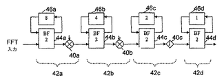
正規のパイプライン型アーキテクチャでは、ただ1つのバタフライ・ユニットが各段階ごとに使われ、完全並列手法での(N/2)log2Nおよび列ベースの手法でのN/2と比較して、合計でlog2Nの計算量となる。16ポイントFFTの長さに対するパイプライン手法の例を、図4に示してある。各段階42a、42bおよび42cの乗算器40は、ハードウェア要件同士を区別するために、バタフライ・ユニット44a、44bおよび44cとは区別される。バタフライ・ユニット44a、44b、44cおよび44dはそれぞれ、各段階ごとのN/2回のバタフライ演算の中で時分割される。バタフライ・ユニット44cを含む段階の場合、乗算器40cは「j」である。最後のバタフライ・ユニット44dの外には、乗算器は必要ない。パイプライン型ベースの実装は、列ベースの手法よりも、FFTフレームごとに、より多くのクロック周期を必要とする。というのは、パイプライン型ベースの手法は、N(radix−2ベースのバタフライ・アーキテクチャを用いるとき)クロック周期中にフルFFTフレームを実装することができ、列手法は、反復時分割構造により、log2N(radix−2ベースのバタフライ・アーキテクチャを用いるとき)クロック周期を必要とするからである。全段階のハードウェア実装において、FFTフレームを処理するクロック数は、障害とはならない。というのは、データは、直列に1フレームずつ挿入され、フレームごとのクロック周期数は、スループットが高いまま、一定の初期遅延に変換されるからである。
Pipelined approach In a regular pipelined architecture, only one butterfly unit is used for each stage, with (N / 2) log 2 N in a fully parallel approach and N / 2 in a column-based approach. In comparison, the total amount of log 2 N is calculated. An example of a pipeline technique for a 16 point FFT length is shown in FIG. The multiplier 40 in each
単一パス遅延フィードバック(SDF)実装については、たとえば、E.H.Wald及びA.M.Despainの「Pipelined and parallel−pipeline FFT processors for VLSI implementation」(IEEE Trans.Comput.、414〜426頁、1984年5月)を参照されたい。この実装は、バタフライ出力をフィードバック・シフト・レジスタまたはFIFO46(そのサイズは図4に与えられており、この例では、レジスタの長さは、相応して8、4、2および1である)に格納することによって、メモリをより効率的に使う。1個のデータ・ストリームが、すべての段階で乗算器を通過する。 For single path delay feedback (SDF) implementations, see, for example, E.I. H. Wald and A.W. M.M. See Despain's “Pipelined and parallel-pipeline FFT processors for VLSI implementation” (IEEE Trans. Comput. 414-426, May 1984). This implementation converts the butterfly output to a feedback shift register or FIFO 46 (its size is given in FIG. 4 and in this example the register lengths are correspondingly 8, 4, 2 and 1). By storing, use memory more efficiently. One data stream passes through the multiplier at all stages.
ハイブリッド手法
ハイブリッド手法は、列およびフィードバック手法の利益を兼ね備える。この手法は、フィードバック手法の要素を使ってメモリを保存し、列段階は、より優れたハードウェア使用に使われる。4ビット幅の列段階バタフライ・ユニットの使用は、より広いBUS幅および適正な再構成可能乗算器の利用と組み合わせることができる。このアーキテクチャは、高い空間使用率およびアルゴリズム効率のために必要な、正確なBUS幅をもつものにコンバートすることもできる。
Hybrid approach The hybrid approach combines the benefits of queue and feedback approaches. This technique uses the elements of the feedback technique to save memory, and the column stage is used for better hardware use. The use of a 4-bit wide column stage butterfly unit can be combined with the use of a wider BUS width and a proper reconfigurable multiplier. This architecture can also be converted to one with the exact BUS width required for high space utilization and algorithm efficiency.
反復プロセスを稼動するポピュラーなアーキテクチャを、図5に示す。このFFT実装は、単一のバタフライ・ユニット50を使用する。この単一バタフライ・ユニット設計は主に、スケジューリングおよびメモリ・アクセス方式の最適化、すなわち、繰り返し時分割された同じバタフライ・ユニットを再利用することによって段階それぞれを実装する際の、パイプライン手法の提供に注力している。Spiffeeプロセッサについては、たとえば、B.M.Baasの「A Low−power、high−performance、1024 point FFT processor」(IEEE Journal of Solid−State Circuits、1999年3月)を参照されたい。このプロセッサは、低電力消費を達成するために、RAM52および乗算器56を含むキャッシュ・メモリ・アーキテクチャを用いて、FFTアルゴリズムの正規のメモリ・アクセス・パターンを活用する例である。コントローラ54として示されるこのプロセッサは、どの長さのFFTも実施するようにプログラミングすることができるが、RAM52によって与えられるキャッシュ・サイズなど、特定の特徴は、特定のFFTサイズ向けにのみ最適化され、この手法は、非常に低い速度で作用する。というのは、Nクロック周期が、パイプライン・アルゴリズムの完全実装によるFFTフレームの計算に必要とされ、一定の初期遅延をもたらすからである。このことは、再利用されるバタフライ・ユニット50による段階の反復時間分割により、フル・フレームは、次のFFTフレームの扱いを始めることができるようになる前に、計算される必要がある(radix−2ベースのバタフライ・ユニットを使うとき、Nクロック周期を必要とする)ことを意味する。
A popular architecture that runs an iterative process is shown in FIG. This FFT implementation uses a
比較的大きいradixベースのバタフライ・ユニット、たとえばRadix−4ベースのアーキテクチャを使うことによって、より効率的なFFTプロセッサを作ることができる。これにより、フルFFTフレームの処理に必要とされる計算クロック・サイクルが、N/2に削減される。高度なDSPおよびチップ内に実装されるFFTアクセラレータのほとんどは、Radix−2またはRadix−4 FFTプロセッサに基づく。こうしたアクセラレータは、使用が限られ(FFT変換用のみ)、非常に低い速度を使用し、高いクロック・レート設計の必要性に苦しむ。 By using a relatively large radix-based butterfly unit, such as a Radix-4 based architecture, a more efficient FFT processor can be made. This reduces the computational clock cycle required to process a full FFT frame to N / 2. Most of the FFT accelerators implemented in advanced DSPs and chips are based on Radix-2 or Radix-4 FFT processors. Such accelerators are limited in use (for FFT conversion only), use very low speeds, and suffer from the need for high clock rate designs.
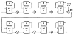
多重パイプライン型手法に基づくフィルタ実装
図6に示すような再構成可能な反復方式を用いると、効率が高いどの種類のフィルタも相関関数も実装することができる。この実装は、図6の60を見ると最もよく分かる、IFFTがその後に続く、フィルタ係数での乗算(時間領域乗算)用の、FFT変換の最終段階の乗算器を使うことによって遂行される。この実装は、FFT/IFFT、たとえば離散コサイン/サイン変換(DCTおよびDST)のどのサブプロダクト、ならびに(等化、予測、補間および相関の計算にも用いることができる)カスケード式FFTおよびIFFTアルゴリズムを用いるフィルタリングのような、上述したアルゴリズムの組合せであるどのアルゴリズムの実装においても効率的である。
Filter Implementation Based on Multiple Pipeline Approach Using a reconfigurable iterative scheme as shown in FIG. 6, any kind of highly efficient filter and correlation function can be implemented. This implementation is accomplished by using a final stage multiplier of the FFT transform for multiplication with filter coefficients (time domain multiplication) followed by IFFT, best seen by looking at 60 in FIG. This implementation uses FFT / IFFT, for example any discrete cosine / sine transform (DCT and DST) sub-products, and cascaded FFT and IFFT algorithms (which can also be used for equalization, prediction, interpolation and correlation calculations). It is efficient in implementing any algorithm that is a combination of the algorithms described above, such as the filtering used.
異なるradixを用いるFFT
radix−22アルゴリズムは、特に関心をもたれている。このアルゴリズムは、radix−4およびsplit−radixアルゴリズムそれぞれと乗算計算量が同じであり、同時に規則的なradix−2バタフライ構造を保持する。この空間的規則性は、VLSI実装用の他のアルゴリズムに勝る、構造上の大きな利点をもたらす。radix−22アルゴリズムの背景にある基本的な考え方は、正規のDIF FFTアルゴリズムの2段階をとり、実数/虚数スワップおよび符号反転のみを伴うW(N/4) N=Jによる自明な乗算の回数を最大にすることにある。言い換えると、FFT係数は再構成され、非自明な乗算は、すべての2段階においてただ1つの複素乗算器が必要とされるように一段階にまとめられる(全体的論理区域を削減する)。図7は、このような係数再構成を表すトレリスを(並列形で)示す。すなわち、どの2つのバタフライ係数、Wi NおよびW(i+(N/4)) Nに対しても、Wi Nが除かれ、次の段階に転送され、この段階は、係数1および
を、対応する位置に残す。この係数再構成を、係数ペアすべてに対して実施した後、一段階が、非自明な乗算なしで残される。
FFT with different radix
radix-2 2 algorithm, it is of particular interest. This algorithm has the same amount of multiplication as the radix-4 and split-radix algorithms, and at the same time maintains a regular radix-2 butterfly structure. This spatial regularity provides significant structural advantages over other algorithms for VLSI implementation. The basic idea behind the radix-2 2 algorithm is the two steps of the regular DIF FFT algorithm, with the obvious multiplication of W (N / 4) N = J with real / imaginary swap and sign inversion only It is to maximize the number of times. In other words, the FFT coefficients are reconstructed and the non-trivial multiplication is combined in one stage (reducing the overall logic area) so that only one complex multiplier is required in all two stages. FIG. 7 shows a trellis representing such a coefficient reconstruction (in parallel form). That is, for any two butterfly coefficients, W i N and W (i + (N / 4)) N , W i N is removed and forwarded to the next stage, which includes the
In the corresponding position. After performing this coefficient reconstruction on all coefficient pairs, one stage is left without non-trivial multiplication.
ハイブリッド・パイプライン/多重化手法
この10年間、いくつかのパイプライン型FFTアーキテクチャが提案されている。シグナル・フロー・グラフの空間規則性は、パイプライン型アーキテクチャにおいて保たれるので、高度にモジュール式であり拡張が容易である。シャッフル・ネットワーク80は、図8Aに示される単一パス遅延フィードバックを介して実装され、ここで、データは、単一パス中の段階82の間で処理され、フィードバックFIFOレジスタ84は、新たな入力および中間結果を格納するのに用いられる。この方式の背景にある基本的な考え方は、データを格納し、次の段階がデータを正しい順序で受け取ることができるようにスクランブルすることである。FIFOレジスタ84が、入力の前半部分で一杯になると、直前の結果の後半部分が、次の段階へシフトアウトされる。この間、演算要素は迂回される。入力の前半部分は、FIFOレジスタからシフトアウトされると、到着した入力の後半と共に処理要素に供給される。この間、演算要素は、2つの出力を操作し生成しており、1つは次の段階82に直接供給され、もう1つは、対応するFIFOレジスタにシフトインされる。乗算器(図示せず)は、必要な場合、radix−22またはradix−2アルゴリズムいずれかに従って、段階の間に挿入される。このような実装において使用するためのトレリスおよびデータ・パケットを、それぞれ図8B、8Cに示してある。
Hybrid pipeline / multiplexing approaches Several pipelined FFT architectures have been proposed over the last decade. The spatial regularity of the signal flow graph is maintained in a pipelined architecture, so it is highly modular and easy to expand. The shuffle network 80 is implemented via single path delay feedback as shown in FIG. 8A, where data is processed during
添付の図面に対して参照が行われるが、同じ参照文字指定をもつ要素は、全体を通して同じ要素を表す。
以下の開示では、変動サイズを有するベクトル(実数ベクトルおよび複素ベクトル)の高速フーリエ変換(FFT)などの直交変換を実施する方法およびシステムを説明する。変換のサイズが、オン・ラインで決定することができ、アルゴリズムへの入力に依存する適合アルゴリズムが実装される。このような適合アルゴリズムの例は、(1)FFT、(2)逆FFT(IFFT)、(3)FFTおよびIFFT、たとえば離散コサイン/サイン変換(DCTおよびDST)の任意のサブプロダクト、(4)ウォルシュ/アダマール変換およびその任意のサブプロダクト、たとえばCDMA、DSSS、拡散/逆拡散コア・アルゴリズム、ならびに上述したアルゴリズムの任意の組合せである。本方法およびシステムは、フィルタリングおよび他の機能に対しても使うことができ、たとえば、FFTおよびIFFTアルゴリズム(このアルゴリズムは、等化、ヒルベルト変換、予測および補間ならびに相関に対しても用いることができる)をカスケードするときに実現することができる。本方法およびシステムは、FFT/IFFTおよび上述したアルゴリズムすべての、高い効率での、かつハードウェアの高速オンライン再構成による広範なパラメータでの実装を可能にする。この実装は、上述した、異なるサイズのいくつかのFFT変換またはアルゴリズムの並列または直列実装用に指定される、装置内のハードウェアの量を大幅に減少させる。 The following disclosure describes a method and system for performing an orthogonal transform, such as a Fast Fourier Transform (FFT) of vectors with varying sizes (real vectors and complex vectors). The size of the transform can be determined online, and an adaptation algorithm is implemented that depends on the input to the algorithm. Examples of such adaptation algorithms are (1) FFT, (2) Inverse FFT (IFFT), (3) FFT and IFFT, eg any sub-product of discrete cosine / sine transform (DCT and DST), (4) Walsh / Hadamard transform and any subproducts thereof, such as CDMA, DSSS, spreading / despreading core algorithm, and any combination of the algorithms described above. The method and system can also be used for filtering and other functions, such as FFT and IFFT algorithms (which can also be used for equalization, Hilbert transform, prediction and interpolation and correlation) ) Can be realized in cascade. The method and system allows implementation of the FFT / IFFT and all of the algorithms described above with a wide range of parameters with high efficiency and hardware fast online reconfiguration. This implementation greatly reduces the amount of hardware in the device specified for the parallel or serial implementation of several FFT transforms or algorithms of different sizes described above.
開示する手法は、FFTベクトルの長さに適合し、それに従ってメモリのサイズを決め、たとえば、シフト・レジスタ(またはFIFO)の長さを変え、相互接続バスを必要に応じて修正し、I/Oブロックの単純な多重化を実現することによって、柔軟性を実現しやすくする簡素化された相互接続構造を提供するように、直交変換プロセッサを修正するものである。入力サンプル・レートでのクロック周波数を使って、FFTの範囲全体を、ハードウェアに直接マップし、より短い長さのFFTには不必要なブロックを無効にすることによって、またはより長い(ただし、より低いシンボル・レートの)ケースの場合は処理段階をたたみ、ハードウェアを時分割することによって、調節することができる。このアーキテクチャは、バッファリングも直列/並列変換も必要としない。 The disclosed technique adapts to the length of the FFT vector, sizes the memory accordingly, eg, changes the length of the shift register (or FIFO), modifies the interconnect bus as needed, By implementing simple multiplexing of O blocks, the orthogonal transform processor is modified to provide a simplified interconnect structure that facilitates flexibility. Use the clock frequency at the input sample rate to map the entire FFT range directly into hardware and disable blocks that are unnecessary for shorter length FFTs or longer (but In the case of lower symbol rates, this can be adjusted by folding the processing steps and time-sharing the hardware. This architecture requires neither buffering nor serial / parallel conversion.
このアーキテクチャは、Radix2、Radix22、Radix23、Radix4、Radix8、または同様の形式を使って、またはそれに従って実装することができる。radix−4(回転係数の乗数なし)は、図9に示すように行列演算として表し、図10のトレリスで示すように実施することもできる。 This architecture can be implemented using or according to Radix2, Radix2 2 , Radix2 3 , Radix4, Radix8, or similar formats. radix-4 (no multiplier of the rotation coefficient) is represented as a matrix operation as shown in FIG. 9, and can also be implemented as shown by the trellis in FIG.
図11に示してある、再構成可能なradix22段階の実装の実施形態は、入力マルチプレクサ111と、2段階のバタフライ・ユニット110aおよび110bと、(符号反転能力をもつ)ただ1つの汎用乗算器114および1つの交差接合ブロック116を有する2つのフィードバック・メモリ112aおよび112bと、コントローラ118とを備える。ブロック116は、IFFTとFFT処理の間を切り換えるのに使われ、そうすることによって、バタフライ・ユニット110aの出力で、乗算器の必要がなくなる。実装において、メモリ112aおよび112bの使用可能メモリのサイズは、処理されるFFTの長さを調節するために、コントローラ118によって修正することができる。変換ベクトルの長さは、検出装置117によって検出し、コントローラ118によって判定することができる。さらに、各計算段階向けの、乗算器114によって使用するための係数を格納するメモリ119が提供される。
The reconfigurable radix2 two- stage implementation shown in FIG. 11 includes an
図12は、16ポイントFFTの、パイプライン型Radix−22(N=16)に基づく実装の実施形態を示す。本実施形態では、コントローラ128は、メモリ、この場合は各段階向けのシフト・レジスタ124それぞれのサイズを設定するための入力を与える。マルチプレクサ121も、第1段階のバタフライ・ユニット122aの入力に所望の順次入力を与えるように設定される。乗算器126a、126bおよび126cは、最初の3段階それぞれの出力の所に別々に位置付けられ、最後の段階は、乗算器を必要としない。図を見ると分かるように、乗算器126aおよび126cは、虚複素「j」に結合される段階の出力を、jで乗算することによって変換する。
FIG. 12 shows an embodiment of a 16-point FFT implementation based on a pipelined Radix-2 2 (N = 16). In this embodiment, the
反復プロセスを実施するアーキテクチャを組み込む代替実施形態を、図13に示す。具体的には、図13は、16ポイントFFTを処理する半パイプライン/反復Radix−22(N=16)に基づく実装の例を示す。本実施形態では、フィードバックを提供する乗算器130bの出力、ならびに変換プロセッサの出力を有する2つのバタフライ段階130aおよび130bのみが必要とされる。具体的には、マルチプレクサ131の出力は、バタフライ・ユニット132aの入力に与えられる。後者は、メモリ(たとえばシフト・レジスタ134aにフィードバックを、および「j」乗算器136aに出力を提供する。「j」乗算器136aの出力は、バタフライ・ユニット132bの入力に加えられる。後者は、メモリ(たとえば、シフト・レジスタ134b)にフィードバックを、および乗算器136bに出力を提供する。出力136bは、フィードバック・パスを介して、バタフライ・ユニット132aの入力に接続される。動作の際、コントローラ138が、メモリ134のサイズを、処理段階に応じて制御する。信号ベクトルが最初に受け取られる第1の事例において、レジスタ134aおよび134bは、それぞれ「8」、「4」で設定され、信号は、2段階を介して処理される。プロセッサの出力は無効にされ、第2段階のバタフライ・ユニット132bの出力は、フィードバック・パスを介して、バタフライ・ユニット132aの入力に加えられる。次の反復中、メモリは、コントローラによって「2」、「1」に設定される。信号は次いで、第2のバタフライ・ユニット132bの出力まで連続して処理される。プロセッサの出力は次いで、有効にされ、フィードバック・パスは、プロセッサの出力が139で与えられるように無効にされる。
An alternative embodiment incorporating an architecture that performs an iterative process is shown in FIG. Specifically, FIG. 13 shows an example implementation based on a half-pipeline / iteration Radix-2 2 (N = 16) that processes a 16-point FFT. In this embodiment, only two
図14は、16ポイント・フィルタの、パイプラインRadix−22(N=16)に基づく実装の例の実施形態を示す。やはり、メモリのサイズは、コントローラ148によって各段階ごとに設定される。フィルタ係数は、乗算器140に加えられる。このアーキテクチャは、反復でもあるいはパイプライン/反復または並列の混合物でもよい。
FIG. 14 illustrates an example embodiment of an implementation of a 16 point filter based on pipeline Radix-2 2 (N = 16). Again, the size of the memory is set for each stage by the
繰り返しになるが、図14のアーキテクチャは、反復あるいはパイプライン/反復または並列アーキテクチャの混合物となるように修正することができる。 Again, the architecture of FIG. 14 can be modified to be iterative or a mixture of pipeline / iteration or parallel architecture.
ウォルシュ/アダマール変換の有効化
行列演算としてのradix−4変換に関する上記の考察から、アーキテクチャは、ウォルシュ拡散/逆拡散関数など、他の直交信号方式を処理するように容易に変えることができることがすぐにに分かる。後者は、乗算係数を、±1の自明なもので単に代用することによって、既存のアーキテクチャを用いて容易に実装することができる。さらに検討すると、非自明な係数および−jで乗算される係数のみが、変更される必要があることが分かる。さらに、非自明な乗算係数は、ウォルシュ拡散/逆拡散関数に必要とされる自明な乗算器の実装に必要なものをすべて、すなわちFFT←→IFFTと、−jでの乗算との間で変化するための能力を、既にもっている。ハードウェアに対する唯一の特別な要件は、コントローラ148を管理することにある。
Enabling the Walsh / Hadamard Transform From the above discussion regarding the radix-4 transform as a matrix operation, it is readily apparent that the architecture can be easily altered to handle other orthogonal signaling schemes, such as Walsh spreading / despreading functions. To understand. The latter can be easily implemented using existing architectures by simply substituting the obvious multiplication factor of ± 1. Further examination shows that only non-trivial coefficients and coefficients multiplied by -j need to be changed. In addition, the non-trivial multiplication factor changes everything necessary for the implementation of the trivial multiplier required for Walsh spreading / despreading functions, ie, FFT ← → IFFT and multiplication at −j. I already have the ability to do that. The only special requirement for hardware is to manage the
一例として、「Radix4」ウォルシュ拡散/逆拡散バタフライ・ユニットは、以下のように、行列演算として表すことができる。
2つの行列表現を比較することによって、2つの変換の間の関係を理解することができる。
radix−4変換は複素演算なので、実数ベクトルに対する2つの独立ウォルシュ拡散/逆拡散プロセスを取得する。というのは、±1での自明な乗数は、IとQ信号の間を入れ替わらないからである。したがって、この特徴は、たとえば、新しいWCDMA標準でのように、2finger RAKE受信機、または複素ウォルシュ拡散/逆拡散関数の実装用に用いることができる。また、第2の独立ウォルシュ拡散/逆拡散関数を、特別段階として使うことも、あるいは、適正な場所で、用意されたIおよびQによって、より大きいウォルシュ拡散/逆拡散用に使うこともできる(この可能性は、図9〜14に示す再構成可能なRadix22アーキテクチャにおいて既に実現されている)。
As an example, a “Radix4” Walsh spreading / despreading butterfly unit can be represented as a matrix operation as follows:
By comparing the two matrix representations, the relationship between the two transformations can be understood.
Since the radix-4 transform is a complex operation, we get two independent Walsh spread / despread processes for real vectors. This is because the obvious multiplier at ± 1 does not interchange between the I and Q signals. Thus, this feature can be used, for example, for implementations of 2finger RAKE receivers, or complex Walsh spreading / despreading functions, as in the new WCDMA standard. The second independent Walsh spreading / despreading function can also be used as a special stage, or can be used for larger Walsh spreading / despreading with the I and Q provided at the right place ( this possibility has already been realized in Radix2 2 architecture reconfigurable shown in Figure 9-14).
図14に提示される実装は、たとえば、NLog(N)回の演算のみを用いて実施されるFFTアルゴリズムを必要とし、したがって、いくつかのコードを併せもつCDMA変調/復調のような演算、すなわち、重いデータ・ロードにとっては非常に効率的である。 The implementation presented in FIG. 14 requires, for example, an FFT algorithm implemented using only NLog (N) operations, and thus operations such as CDMA modulation / demodulation with several codes combined, ie It is very efficient for heavy data loads.
ここで、複素乗算器は、擬似ランダム・シーケンスを有するウォルシュ・シーケンスを、非常に高い効率でランダム化し/非ランダム化する、周波数領域内でのフィルタの実装において使うことができる(いくつかのコードを併せもつCDMA変調/復調を扱うとき、すなわち、重いデータ・ロードの場合(CDMA/WCDMA標準において見られるように)。この効率性は、変調されたデータを(コードすべてに対して)一度だけ乗算する必要があり、すべてのコードが別々に乗算されるのではないおかげで実現される。 Here, the complex multiplier can be used in the implementation of a filter in the frequency domain that randomizes / derandomizes Walsh sequences with pseudo-random sequences with very high efficiency (some codes When dealing with CDMA modulation / demodulation, ie, in the case of heavy data loads (as seen in the CDMA / WCDMA standard), this efficiency is only once for the modulated data (for all codes) This is achieved thanks to the need to multiply and not all code is multiplied separately.
図15は、ウォルシュ・コードをランダム化する回転乗数が、並列アーキテクチャの最初および最後で使われるときのウォルシュ拡散/逆拡散関数へのradix−4段階の変換の実施形態の例のトレリスを示す。図15は具体的には、16ポイント・ウォルシュ拡散/逆拡散関数の並列Radix−22(N=16)に基づく実装の例を示す。
かっkお
回転乗数を使ってradix−2ベースのFFTを実施すると、乗数は、「1」にのみ変えることができる。図16は、16ポイントの、ウォルシュ拡散/逆拡散シーケンスの並列Radix−2(N=16)に基づく実装のトレリスの例、すなわち、変調/復調中の一連の16チップのウォルシュ拡散/逆拡散シーケンスの例を示す。
FIG. 15 shows an example trellis of an embodiment of a radix-4 stage conversion to a Walsh spreading / despreading function when the rotation multiplier that randomizes the Walsh code is used at the beginning and end of the parallel architecture. FIG. 15 specifically shows an example of an implementation based on parallel Radix-2 2 (N = 16) of 16-point Walsh spreading / de-spreading functions.
When a radix-2 based FFT is performed using a rotation multiplier, the multiplier can only be changed to “1”. FIG. 16 shows an example of a trellis of an implementation based on a parallel 16-point Walsh spread / despread sequence Radix-2 (N = 16), ie a series of 16 chips Walsh spread / despread sequence during modulation / demodulation An example of
やはり、複素乗算器を上で説明したように、たとえば周波数領域内のフィルタの実装に、または擬似ランダム・シーケンスを有するウォルシュ・シーケンスのランダム化/非ランダム化に使うことができる。効率性は、変調されたデータを(コードすべてに対して)一度だけ乗算する必要があり、したがって各コードが別々に乗算されるわけではないおかげで実現される。 Again, complex multipliers can be used as described above, for example in the implementation of filters in the frequency domain, or in the randomization / non-randomization of Walsh sequences with pseudo-random sequences. Efficiency is achieved thanks to the need to multiply the modulated data only once (for all codes) and thus not each code being multiplied separately.
再構成可能なハイブリッド・パイプライン列の多重化手法
図17に示すように、4ビット幅の小さいradix22バタフライ・ユニットの「バンク」を組み合わせて、より広いBUS radix22を形成することができ、小さいRadixはそれぞれ、組合せ/分裂することができる、RAMの再構成可能な制御された「バンク」に接続される。BUS分裂用の再構成可能な乗算器は、上記方法に基づいて、非常に高い使用率および低電力消費である、任意の長さのIFFT/FFT/フィルタ/相関器およびウォルシュ/アダマール変換またはその任意の下位プロダクト、たとえば、CDMA DSSSコアもしくはDDS周波数フィルタも有する、再構成可能な「処理」コアを用いて実装することもでき、様々な並列/パイプライン/反復アルゴリズム・アーキテクチャ方式を含むいくつかのアルゴリズムがどの構成中でも稼動することができるとき、任意のBUS幅が必要になる。シリコンでのコアの実装は、最大クロック・レートを有するので、必要性による再構成は、任意の数の並列/パイプライン/反復アルゴリズム・アーキテクチャ方式をもたらし、各々が、いつでもアルゴリズムおよびシリコン実装資源用に、かつモデム実装のどの標準に対しても最適化され、したがって、高い使用性能を有する非常に小型の再構成アーキテクチャをもたらす。図17は、FFT/IFFTベクトルを処理する再構成可能なME−Iコアの例を示す。
Reconfigurable Hybrid Pipeline Array Multiplexing Technique As shown in FIG. 17, the “bank” of radix2 2 butterfly units with a small 4 bit width can be combined to form a wider BUS radix2 2 , Each small Radix is connected to a reconfigurable controlled “bank” of RAM that can be combined / split. Based on the above method, a reconfigurable multiplier for BUS splitting is an IFFT / FFT / filter / correlator and Walsh / Hadamard transform of any length that has very high utilization and low power consumption. Some sub-products can also be implemented using a reconfigurable “processing” core, which also has a CDMA DSSS core or a DDS frequency filter, and several including various parallel / pipeline / iteration algorithm architecture schemes When any of the above algorithms can be operated in any configuration, an arbitrary BUS width is required. Since the core implementation in silicon has a maximum clock rate, reconfiguration by necessity results in any number of parallel / pipeline / iteration algorithm architecture schemes, each for algorithm and silicon implementation resources at any time And is optimized for any standard of modem implementation, thus resulting in a very compact reconfiguration architecture with high usage performance. FIG. 17 shows an example of a reconfigurable ME-I core that processes FFT / IFFT vectors.
本開示を要約すると、現在の手法は、簡素化された相互接続構造を用いることによる、基本FFTプロセッサの修正を含む。こうすることにより、メモリのシフト・レジスタ(またはFIFO)の長さを単に変えること、バス・サイズを必要に応じて変えること、I/Oブロックのシンプル多重化によってFFTのサイズを調整する際の柔軟性が実現される。入力サンプル・レートでのクロック周波数を使って、FFTの範囲全体を、ハードウェアに直接マップし、より短い長さのFFTには不必要なブロックを無効にすることによって、またはより長い(ただし、より遅いシンボル・レートの)ケースの場合は処理段階をたたみ、ハードウェアを時分割することによって、調節することができる。このアーキテクチャは、バッファリングも直列/並列変換も必要としない。 To summarize this disclosure, the current approach involves a modification of the basic FFT processor by using a simplified interconnect structure. This allows you to simply change the length of the memory shift register (or FIFO), change the bus size as needed, and adjust the FFT size by simple multiplexing of I / O blocks. Flexibility is realized. Use the clock frequency at the input sample rate to map the entire FFT range directly into hardware and disable blocks that are unnecessary for shorter length FFTs or longer (but In the case of slower symbol rates, this can be adjusted by folding the processing steps and time-sharing the hardware. This architecture requires neither buffering nor serial / parallel conversion.
一例として、Radix22アーキテクチャを用いると、(回転係数の乗数のない)radix−4は、図9に見られる行列演算としても表すことができる。対応するバタフライ構造を、図10に提示してある。したがって、上記の例に示すように、radix22段階の実装は、ただ1つの汎用乗算器を有する2段階のバタフライ・ユニットと、符号乗算を伴う1つの交差接合(IFFT/FFT変化にも必要とされる)とを必要とし、こうすることにより、乗算器の必要がなくなる。対応する構造を、図11に提示してある。16ポイントFFTのRadix22実装の対応する多段階実装(図4を参照)が、図12で与えられる。同じであるが、再構成可能な反復スイッチ機構を用いて実装される変換を、図13(一段階)および図14(多段階)に提示してある。 As an example, the use of Radix2 2 architecture, (multiplier without the rotation factor) radix-4 can also be expressed as a matrix operation seen in FIG. A corresponding butterfly structure is presented in FIG. Thus, as shown in the example above, the implementation of radix2 two- stage is required for a two-stage butterfly unit with only one general-purpose multiplier and one cross-junction with sign multiplication (IFFT / FFT change). This eliminates the need for a multiplier. The corresponding structure is presented in FIG. Radix2 2 implementation of the corresponding multi-stage implementation of the 16-point FFT (see Figure 4) is given in Figure 12. A transformation implemented using the same but reconfigurable repetitive switch mechanism is presented in FIG. 13 (one stage) and FIG. 14 (multistage).
ウォルシュ/アダマール変換の有効化:FFT/IFFTに関連して以上のように説明したプロセッサおよび方法は、他の変換用のプロセッサおよび方法を実装するのに使うこともできる。行列演算としてのradix−4変換の上記提示から、演算をウォルシュ拡散/逆拡散関数に変えるために必要とされることは、FFT用に使われる乗数を、±1の自明な乗数で代用することだけである。さらに検討すると、非自明なもの、および−jで乗算されるものだけが、変更される必要があることが分かる。さらに、FFT←→IFFTの間で変化させ、−jで乗算するための能力をもつ、非自明な乗数だけが、ウォルシュ拡散/逆拡散に必要とされる自明な乗数の実装に必要である。ハードウェアに対するただ1つの特別な要件は、プロセッサの動作を管理し制御するコントローラにある。 Enabling the Walsh / Hadamard Transform: The processors and methods described above in connection with FFT / IFFT can also be used to implement processors and methods for other transforms. From the above presentation of the radix-4 transform as a matrix operation, what is needed to change the operation to Walsh diffusion / despreading function is to substitute the multiplier used for FFT with an obvious multiplier of ± 1. Only. Further examination shows that only the non-obvious ones and those multiplied by -j need to be changed. Furthermore, only non-trivial multipliers with the ability to vary between FFT ← → IFFT and multiply by −j are necessary for the implementation of the trivial multipliers required for Walsh spreading / despreading. The only special requirement for hardware is a controller that manages and controls the operation of the processor.
「Radix4」ウォルシュ拡散/逆拡散バタフライは、下に示すように、行列演算としても表すことができる。
図17に提示される実装は、たとえば、NLog(N)回の演算のみを必要とし、いくつかのコードを併せもつCDMA変調/復調、すなわち、重いデータ・ロードにとっては非常に効率的である。 The implementation presented in FIG. 17 requires only NLog (N) operations, for example, and is very efficient for CDMA modulation / demodulation with several codes, ie heavy data loading.
ここで、複素乗算器は、擬似ランダム・シーケンスを有するウォルシュ・シーケンスを、非常に高い効率でランダム化し/非ランダム化する、周波数領域内でのフィルタのような構成の実装に使うことができる(いくつかのコードを併せもつCDMA変調/復調を扱うとき、すなわち、重いデータ・ロードの場合(CDMA/WCDMA標準において見られるように)。この効率は、変調されたデータを(コードすべてに対して)一度だけ乗算する必要があり、すべてのコードが別々に乗算されるのではないおかげで達成される。 Here, the complex multiplier can be used to implement a filter-like configuration in the frequency domain that randomizes / non-randomizes Walsh sequences with pseudo-random sequences ( When dealing with CDMA modulation / demodulation with several codes, ie in case of heavy data load (as seen in the CDMA / WCDMA standard), this efficiency can be obtained by This is achieved thanks to having to multiply only once and not all code is multiplied separately.
図15は、ウォルシュ・コードをランダム化する回転乗数が並列アーキテクチャにおいて必要とされるとき(開始/最後)のウォルシュ拡散/逆拡散関数へのradix−4段階の変換を提示する。Radix−2ベースのFFTの例の場合、回転乗数は、「1」にのみ変更される必要がある。変調/復調処理のための16チップのウォルシュ拡散/逆拡散シーケンスの例を、図16に示す。複素乗算器を上で説明したように、たとえば周波数領域内のフィルタの実装に、または擬似ランダム・シーケンスを有するウォルシュ・シーケンスのランダム化/非ランダム化に使うことができる。変調されたデータを(コードすべてに対して)一度だけ乗算する必要があるおかげで、効率性が実現される。各コードは、別々に乗算される必要がない。 FIG. 15 presents a radix-4 stage conversion to a Walsh spreading / despreading function when a rotation multiplier that randomizes the Walsh code is needed in the parallel architecture (start / end). In the case of the Radix-2 based FFT example, the rotation multiplier only needs to be changed to “1”. An example of a 16-chip Walsh spread / despread sequence for modulation / demodulation processing is shown in FIG. Complex multipliers can be used as described above, for example in the implementation of filters in the frequency domain, or for randomization / non-randomization of Walsh sequences with pseudo-random sequences. Efficiency is achieved thanks to the need to multiply the modulated data only once (for all codes). Each code need not be multiplied separately.
再構成可能なハイブリッド・パイプライン列多重化手法
最後に、一般直交変換を実装する再構成可能な装置の全体アーキテクチャを、Radix2i/xバタフライ変換の場合の図18に簡単に示す。計算ユニットは、Radix2、Radix22、Radix23、Radix4、Radix8などのバタフライ・ユニットを使用して実装することができる。この装置は好ましくは、再構成可能なRAMクラスタおよび再構成可能なBUSマルチプレクサ・ブロック180、1つまたは複数のバタフライ・ユニットを備える計算ユニット182、再構成可能な乗算器ブロック184、制御および記憶ユニット186ならびに検出装置188を備える。変換の各段階で、ユニット186は、2のバタフライ・ユニット内の乗算器の係数を、変換に従って修正する(対応する係数は、値{−1,1,j,−j}をとり得る)。ユニット182による演算の結果は、ユニット180(やはりユニット186によって制御される)のレジスタに格納される。レジスタのサイズは、段階ごとに変更される。格納されたデータの一部は、再構成可能な乗算器ブロック184に挿入され、データは、段階およびアルゴリズムに従って、制御および記憶ユニット186によって確立された係数で乗算される。乗算の結果は、ブロック180に格納される。ブロック180のマルチプレクサは、格納されたデータの多重化に使われる。各段階ごとにわずか1つのバタフライ・ユニットおよび1つのマルチプレクサを使えばよく、この1つのバタフライ・ユニットおよび乗算器は、ハードウェアを単に再構成することによって、各段階向けに再利用することができることが明らかであろう。
Reconfigurable Hybrid Pipeline Sequence Multiplexing Technique Finally, the overall architecture of a reconfigurable device implementing the general orthogonal transform is briefly shown in FIG. 18 for the Radix2 i / x butterfly transform. The computing unit can be implemented using butterfly units such as Radix2, Radix2 2 , Radix2 3 , Radix4, Radix8. The apparatus preferably includes a reconfigurable RAM cluster and a reconfigurable
上述した内容の具体的なアプリケーションが、参照によって組み込まれている、2005年3月3日に出願した、「Low−Power Reconfigurable Architecture For Simultaneous Implementation Of Distinct Communication Standards」という名称の、我々の同時継続出願第11/071,340号(整理番号66940−021)に記載されている。図18は、この同時継続出願において記載され権利請求されているシステムのブロック図を示す。 A specific application of the above content is incorporated by reference, filed on Mar. 3, 2005, “Continuation of our application named“ Low-Power Reconfigurable Architecture for Simulative Implementation Of Distinct Communication Standards ””. No. 11 / 071,340 (reference number 66940-021). FIG. 18 shows a block diagram of the system described and claimed in this co-pending application.
したがって、図19に示すように、上で述べたチップ・アーキテクチャ要件に従うようになされた集積チップの実施形態は、以下の基本的な機能構成要素を備える。 Accordingly, as shown in FIG. 19, an embodiment of an integrated chip adapted to comply with the chip architecture requirements described above comprises the following basic functional components:
CPU190は好ましくは、(a)装置のconfigware部、すなわち、ネット・バス192、I/Oブロック194、RAMブロック196、メガファンクション・ブロック(群)198、相互接続ブロック200、フラッシュ・メモリ・ブロック202およびクロック204を制御し、(b)メガファンクション・ブロック(群)198、ならびにバス192、I/Oブロック194、RAMブロック196、相互接続ブロック200、フラッシュ・メモリ・ブロック202およびクロック204の構成を、チップによって処理される信号のプロトコルに応じて固定するのに必要とされる、比較的小さいコンピュータ処理ユニットである。CPU190は、比較的重要でなく単純な割当てまたはタスクを計算し、メガファンクションおよびI/Oブロックを相互接続するのに使われるバスを構成するのを助けることもできる。
The
ネット・バス192は、プロトコルに応じて再構成可能である。I/Oブロック194は好ましくは、チップを外界と接続する、構成可能なI/Oブロックである。そのタスクは、アプリケーション・アルゴリズムの「コンパイルされたソフトウェア」を受け取ること、および入力データを受け取り、出力処理されたデータを届けることを含む。RAM196は、好ましくは「コンパイルされたソフトウェア命令」を格納するように、かつデータをキャッシュに入れバッファに入れるように構成されたランダム・アクセス・メモリである。メガファンクション・ブロック198は好ましくは、2つ以上のアプリケーション、すなわち、アプリケーション機能の各ドメインを、一機能として並外れた効率で計算することによって処理されるプロトコルからなる比較的重要なアプリケーション機能を含むように構成される。本ケースでは、メガファンクション・ブロック198は、本明細書において説明した直交変換の1つまたは複数、あるいはそのどの組合せも含むように構成される。相互接続ブロック200は好ましくは、CPU190、I/Oブロック194、RAM196、メガファンクション・ブロック198、ならびにフラッシュ・メモリ202およびクロック・ブロック204を含む、チップの構成要素をすべて接続する再構成可能なネット・バスを含む。相互接続ブロックは、比較的重要でなく単純な割当てまたはタスクを、好ましくは余分メモリ内で実施するように構成することもできる。最後に、フラッシュ・メモリ200は好ましくは、チップがそのプログラムを介して稼動するとき、データを格納するように働く。フラッシュ・メモリは好ましくは、一度のプログラミング動作で多数の記憶場所を消去させ、またはそこに書き込ませ、そうすることによって、それを使うシステムが、異なる場所で同時に読み取り、書き込むときに、より高い実効速度で動作することができるEEPROMの形である。より少ない複素演算用には、他のタイプのメモリを使ってよいことが理解されるべきである。情報は好ましくは、チップ内に情報を維持するのに電力を必要としないやり方で情報をシリコン・チップ上に格納することによって、フラッシュ・メモリに格納される。したがって、チップへの電力を絶つことができ、電力を全く消費することなく、情報がフラッシュ・メモリに保持される。さらに、フラッシュ・メモリは、高速読取りアクセス時間および固体衝撃抵抗を提供し、フラッシュ・メモリを、セルラー電話およびPDAのような、電池で動く装置におけるデータ記憶装置などのアプリケーションにおいて特に望ましいものにする。
The
ここまで説明したアーキテクチャはしたがって、集積回路として実装することができる。本アーキテクチャは、ベクトル(実数ベクトルおよび複素ベクトル両方)がサイズを変化させ得る、どのタイプの直交信号方式にも適合可能と考えられる。このような直交信号方式は、FFT変換、逆FFT変換(IFFT)または離散コサイン/サイン変換(DCTおよびDST)のようなその任意のサブプロダクト、ウォルシュ/アダマール変換またはCDMA DSSS拡散/逆拡散のようなその任意のサブプロダクト、こうしたアルゴリズムの2つ以上の組合せである任意のアルゴリズム、ならびに、等化、ヒルベルト変換、予測、補間、相関などにも使うことができる、このような他の機能、たとえば、FFTおよびIFFT変換の連結を用いることによるフィルタリングを含み得るが、それに制約されない。 The architecture described so far can therefore be implemented as an integrated circuit. The architecture is considered adaptable to any type of orthogonal signaling where vectors (both real and complex vectors) can vary in size. Such an orthogonal signaling scheme can be any sub-product such as FFT transform, inverse FFT transform (IFFT) or discrete cosine / sine transform (DCT and DST), Walsh / Hadamard transform or CDMA DSSS spreading / despreading. Any such sub-product, any algorithm that is a combination of two or more of these algorithms, and other such functions that can also be used for equalization, Hilbert transform, prediction, interpolation, correlation, etc. , Filtering by using concatenation of FFT and IFFT transforms, but is not limited thereto.
本明細書で開示した本開示のアーキテクチャ、およびその全要素は、添付の特許請求の範囲の少なくとも1つの範囲内に含まれる。ここで開示したチップ・アーキテクチャのどの要素も、権利放棄されることも意味しているのではなく、必ずしも特許請求の範囲の解釈を制限することも意図していない。 The disclosed architecture and all elements disclosed herein are within the scope of at least one of the appended claims. None of the elements of the chip architecture disclosed herein is meant to be waived, nor is it necessarily intended to limit the interpretation of the claims.
Claims (30)
1つまたは複数のバタフライ・ユニットを含むように構成され配置された計算ユニットと、
前記計算ユニットの出力に結合され、前記変換の少なくとも1つの段階向けの前記バタフライ演算をすべて実施するように構成され配置された1つまたは複数の乗算器を含むブロックと、
各バタフライ演算を実施する前記計算ユニットによる使用のために、前記バタフライ演算の中間結果および所定の係数を格納するように構成され配置された記憶ユニットであって、メモリおよび多重化アーキテクチャを含む前記記憶ユニットと、前記変換の前記バタフライ演算すべてを、前記段階用にただ1つの計算ユニットが必要とされるように前記一段階向けの前記計算ユニットを使って時分割するように構成され配置されたマルチプレクサ・ユニットと、
前記計算ユニットに係数を与え、前記記憶ユニット内のメモリのサイズおよび多重化アーキテクチャを制御するように構成され配置されたコントローラとを備え、
各段階用の、前記乗算器の係数、前記計算ユニットの前記係数、メモリのサイズ、および多重化アーキテクチャが、Nの値に応じて修正される、再構成可能なアーキテクチャ。 A reconfigurable architecture that performs fast orthogonal transformation of vectors in multiple stages, the size of the vector is N, N may vary, and the number of stages is a function of N;
A computing unit constructed and arranged to include one or more butterfly units;
A block including one or more multipliers coupled to the output of the computing unit and configured and arranged to perform all the butterfly operations for at least one stage of the transformation;
A storage unit configured and arranged to store intermediate results of the butterfly operation and predetermined coefficients for use by the computing unit performing each butterfly operation, the memory comprising a memory and a multiplexing architecture And a multiplexer configured and arranged to time-divide all the butterfly operations of the transformation using the computing unit for the stage so that only one computing unit is required for the stage・ Unit and
A controller configured and arranged to provide coefficients to the computing unit and to control the size and multiplexing architecture of the memory in the storage unit;
A reconfigurable architecture, wherein for each stage the multiplier coefficients, the coefficients of the computing unit, the size of the memory, and the multiplexing architecture are modified according to the value of N.
1つまたは複数のバタフライ・ユニットを含むように構成され配置された計算ユニットと、
前記計算ユニットの出力に結合され、前記変換の少なくとも1つの段階向けの前記バタフライ演算をすべて実施するように構成され配置された1つまたは複数の乗算器を含むブロックと、
各バタフライ演算を実施する前記計算ユニットによる使用のために、前記バタフライ演算の中間結果および所定の係数を格納するように構成され配置された記憶ユニットであって、メモリおよび多重化アーキテクチャを含む前記記憶ユニットと、
メモリおよび多重化アーキテクチャを含む前記記憶ユニットと、
前記変換の前記バタフライ演算すべてを、前記段階用にただ1つの計算ユニットが必要とされるように前記一段階向けの前記計算ユニットを使って時分割するように構成され配置されたマルチプレクサ・ユニットと、
前記計算ユニットに係数を与え、前記記憶ユニット内のメモリのサイズおよび多重化アーキテクチャを制御するように構成され配置されたコントローラとを備え、
各段階用の、前記乗算器の係数、前記計算ユニットの前記係数、メモリのサイズ、および多重化アーキテクチャが、Nの値に応じて修正される集積チップ。 An integrated chip with a reconfigurable architecture that performs fast orthogonal transformation of vectors in multiple stages, the size of the vector is N, N may vary, and the number of stages is a function of N; The architecture is
A computing unit constructed and arranged to include one or more butterfly units;
A block comprising one or more multipliers coupled to the output of the computing unit and configured and arranged to perform all the butterfly operations for at least one stage of the transformation;
A storage unit configured and arranged to store intermediate results and predetermined coefficients of the butterfly operation for use by the computing unit performing each butterfly operation, the memory comprising a memory and a multiplexing architecture Unit,
Said storage unit comprising a memory and a multiplexing architecture;
A multiplexer unit configured and arranged to time-share all the butterfly operations of the transformation using the computing unit for the stage so that only one computing unit is required for the stage; ,
A controller configured and arranged to provide coefficients to the computing unit and to control the size and multiplexing architecture of the memory in the storage unit;
An integrated chip in which, for each stage, the coefficients of the multiplier, the coefficients of the computing unit, the size of the memory, and the multiplexing architecture are modified according to the value of N.
計算ユニットを、1つまたは複数のバタフライ・ユニットを含むように、ブロックを、前記計算ユニットの出力に結合された1つまたは複数の乗算器を含むように構成し配列し、前記1つまたは複数のバタフライ・ユニットおよび1つまたは複数の乗算器を、前記変換の少なくとも1つの段階向けの前記バタフライ演算をすべて実施するように構成し配列すること、
各バタフライ演算を実施する前記計算ユニットによる使用のために、前記バタフライ演算の中間結果および所定の係数を記憶ユニットに格納することであって、前記記憶ユニットは、メモリおよび多重化アーキテクチャを含むこと、
前記変換の前記バタフライ演算すべてを、前記段階用にただ1つの計算ユニットが必要とされるように前記一段階向けの前記計算ユニットを使って時分割すること、ならびに
前記計算ユニットに係数を与え、前記記憶ユニット内のメモリのサイズおよび多重化アーキテクチャを制御することを含み、
各段階用の、前記乗算器の係数、前記計算ユニットの前記係数、メモリのサイズ、および多重化アーキテクチャが、Nの値に応じて修正される方法。 A method of performing a fast orthogonal transformation of a vector in multiple stages, where the size of the vector is N, N may vary, the number of stages is a function of N,
Configuring and arranging the block to include one or more multipliers coupled to an output of the calculation unit, such that the calculation unit includes one or more butterfly units; Configuring and arranging the butterfly unit and one or more multipliers to perform all the butterfly operations for at least one stage of the transformation;
Storing an intermediate result of the butterfly operation and a predetermined coefficient in a storage unit for use by the computing unit performing each butterfly operation, the storage unit comprising a memory and a multiplexing architecture;
Time-sharing all the butterfly operations of the transformation using the computing unit for the stage so that only one computing unit is needed for the stage, and giving coefficients to the computing unit; Controlling the size and multiplexing architecture of the memory in the storage unit;
A method in which, for each stage, the coefficients of the multiplier, the coefficients of the calculation unit, the size of the memory and the multiplexing architecture are modified according to the value of N.
前記計算ユニットが、前記変換の少なくとも1つの段階向けの前記バタフライ演算すべてを実施することができるように、少なくとも1つの計算ユニットを、少なくとも1つのバタフライ・ユニットおよび前記バタフライ・ユニットの出力に結合された乗算器を含むように構成し配列することができるように構成され配置された、再構成可能な一群のバタフライ・ユニットおよび再構成可能な1組の乗算器、ならびに前記バタフライ演算の中間結果および各バタフライ演算の実施において使用するための所定の係数を格納するように前記計算ユニットに結合された再構成可能なメモリを使用することを含み、
各段階用の係数およびメモリのサイズが、Nの値に応じて修正される方法。 A method of performing a fast orthogonal transformation of a vector in multiple stages, where the size of the vector is N, N may vary, the number of stages is a function of N,
At least one computing unit is coupled to at least one butterfly unit and the output of the butterfly unit so that the computing unit can perform all the butterfly operations for at least one stage of the transformation. A reconfigurable group of butterfly units and a reconfigurable set of multipliers configured and arranged to include and can be arranged to include intermediate multipliers, and intermediate results of the butterfly operations and Using a reconfigurable memory coupled to the computing unit to store predetermined coefficients for use in performing each butterfly operation;
A method in which the coefficients for each stage and the size of the memory are modified according to the value of N.
前記計算ユニットが、前記変換の少なくとも1つの段階向けの前記バタフライ演算すべてを実施することができるように、少なくとも1つの計算ユニットを、少なくとも1つのバタフライ・ユニットおよび前記バタフライ・ユニットの出力に結合された乗算器を含むように構成し配列することができるように構成され配置された、再構成可能な一群のバタフライ・ユニットおよび再構成可能な1組の乗算器、ならびに前記バタフライ演算の中間結果および各バタフライ演算の実施において使用するための所定の係数を格納するように前記計算ユニットに結合された再構成可能なメモリを使用することを含み、
各段階用の係数およびメモリのサイズが、Nの値に応じて修正されるシステム。
A system that performs fast orthogonal transformation of a vector in multiple stages, the size of the vector is N, N may vary, the number of stages is a function of N,
At least one computing unit is coupled to at least one butterfly unit and the output of the butterfly unit so that the computing unit can perform all of the butterfly operations for at least one stage of the transformation. A reconfigurable group of butterfly units and a reconfigurable set of multipliers configured and arranged to be configured and arranged to include a plurality of multipliers, and intermediate results of the butterfly operations and Using a reconfigurable memory coupled to the computing unit to store predetermined coefficients for use in performing each butterfly operation;
A system in which the coefficients for each stage and the size of the memory are modified according to the value of N.
Applications Claiming Priority (7)
| Application Number | Priority Date | Filing Date | Title |
|---|---|---|---|
| US58639104P | 2004-07-08 | 2004-07-08 | |
| US58635304P | 2004-07-08 | 2004-07-08 | |
| US58638904P | 2004-07-08 | 2004-07-08 | |
| US58639004P | 2004-07-08 | 2004-07-08 | |
| US60425804P | 2004-08-25 | 2004-08-25 | |
| US11/071,340 US7568059B2 (en) | 2004-07-08 | 2005-03-03 | Low-power reconfigurable architecture for simultaneous implementation of distinct communication standards |
| PCT/US2005/024063 WO2006014528A1 (en) | 2004-07-08 | 2005-07-08 | A method of and apparatus for implementing fast orthogonal transforms of variable size |
Publications (2)
| Publication Number | Publication Date |
|---|---|
| JP2008506191A true JP2008506191A (en) | 2008-02-28 |
| JP2008506191A5 JP2008506191A5 (en) | 2008-08-21 |
Family
ID=35787416
Family Applications (1)
| Application Number | Title | Priority Date | Filing Date |
|---|---|---|---|
| JP2007520491A Pending JP2008506191A (en) | 2004-07-08 | 2005-07-08 | Method and apparatus for performing variable size fast orthogonal transform |
Country Status (6)
| Country | Link |
|---|---|
| EP (1) | EP1769391A1 (en) |
| JP (1) | JP2008506191A (en) |
| KR (1) | KR101162649B1 (en) |
| AU (1) | AU2005269896A1 (en) |
| CA (1) | CA2563450A1 (en) |
| WO (1) | WO2006014528A1 (en) |
Cited By (8)
| Publication number | Priority date | Publication date | Assignee | Title |
|---|---|---|---|---|
| WO2009110022A1 (en) * | 2008-03-03 | 2009-09-11 | 富士通株式会社 | Wireless communication device |
| WO2013042249A1 (en) * | 2011-09-22 | 2013-03-28 | 富士通株式会社 | Fast fourier transform circuit |
| WO2014013726A1 (en) * | 2012-07-18 | 2014-01-23 | 日本電気株式会社 | Fft circuit |
| JPWO2013042249A1 (en) * | 2011-09-22 | 2015-03-26 | 富士通株式会社 | Fast Fourier transform circuit |
| US9880975B2 (en) | 2013-12-13 | 2018-01-30 | Nec Corporation | Digital filter device, digital filter processing method, and storage medium having digital filter program stored thereon |
| US9934199B2 (en) | 2013-07-23 | 2018-04-03 | Nec Corporation | Digital filter device, digital filtering method, and storage medium having digital filter program stored thereon |
| JP2019511056A (en) * | 2016-04-01 | 2019-04-18 | エイアールエム リミテッド | Complex multiplication instruction |
| WO2021157172A1 (en) * | 2020-02-06 | 2021-08-12 | 三菱電機株式会社 | Complex multiplication circuit |
Families Citing this family (5)
| Publication number | Priority date | Publication date | Assignee | Title |
|---|---|---|---|---|
| FR2935819B1 (en) * | 2008-09-05 | 2010-09-10 | Commissariat Energie Atomique | DIGITAL PROCESSING DEVICE FOR FOURIER TRANSFORMATION AND FINAL IMPULSE RESPONSE FILTERING |
| CN102737007B (en) * | 2011-04-07 | 2015-01-28 | 中兴通讯股份有限公司 | Method and device supporting random replacement of plurality of data units |
| KR101275087B1 (en) | 2011-10-28 | 2013-06-17 | (주)에프씨아이 | Ofdm receiver |
| KR102155770B1 (en) * | 2018-11-27 | 2020-09-14 | 한국항공대학교산학협력단 | Scalable fast Fourier transform apparatus and method based on twice perfect shuffle network for radar applications |
| CN113111300B (en) * | 2020-01-13 | 2022-06-03 | 上海大学 | Fixed point FFT implementation system with optimized resource consumption |
Citations (7)
| Publication number | Priority date | Publication date | Assignee | Title |
|---|---|---|---|---|
| JPH02504682A (en) * | 1987-08-21 | 1990-12-27 | コモンウエルス・サイエンティフィック・アンド・インダストリアル・リサーチ・オーガニゼイション | Conversion processing circuit |
| US5293330A (en) * | 1991-11-08 | 1994-03-08 | Communications Satellite Corporation | Pipeline processor for mixed-size FFTs |
| WO1997019412A1 (en) * | 1995-11-17 | 1997-05-29 | Teracom Svensk Rundradio | Improvements in or relating to real-time pipeline fast fourier transform processors |
| JP2001514771A (en) * | 1997-01-06 | 2001-09-11 | ジョンソン、ロバート・ダブリュ | Dimensionless fast Fourier transform method and apparatus |
| JP2002501253A (en) * | 1998-01-21 | 2002-01-15 | テレフオンアクチーボラゲット エル エム エリクソン(パブル) | High-speed pipelined Fleier transform processor |
| JP2002215605A (en) * | 2001-01-19 | 2002-08-02 | Sony Corp | Operation system |
| JP2004153800A (en) * | 2002-10-07 | 2004-05-27 | Matsushita Electric Ind Co Ltd | Communication device and communication device reconstructing method |
Family Cites Families (3)
| Publication number | Priority date | Publication date | Assignee | Title |
|---|---|---|---|---|
| JPH11143860A (en) | 1997-11-07 | 1999-05-28 | Matsushita Electric Ind Co Ltd | Orthogonal transformer |
| JP2001156644A (en) * | 1999-11-29 | 2001-06-08 | Fujitsu Ltd | Orthogonal transform device |
| US20030055861A1 (en) * | 2001-09-18 | 2003-03-20 | Lai Gary N. | Multipler unit in reconfigurable chip |
-
2005
- 2005-07-08 CA CA002563450A patent/CA2563450A1/en not_active Abandoned
- 2005-07-08 KR KR1020077003027A patent/KR101162649B1/en not_active IP Right Cessation
- 2005-07-08 WO PCT/US2005/024063 patent/WO2006014528A1/en active Application Filing
- 2005-07-08 AU AU2005269896A patent/AU2005269896A1/en not_active Abandoned
- 2005-07-08 JP JP2007520491A patent/JP2008506191A/en active Pending
- 2005-07-08 EP EP05768342A patent/EP1769391A1/en not_active Withdrawn
Patent Citations (7)
| Publication number | Priority date | Publication date | Assignee | Title |
|---|---|---|---|---|
| JPH02504682A (en) * | 1987-08-21 | 1990-12-27 | コモンウエルス・サイエンティフィック・アンド・インダストリアル・リサーチ・オーガニゼイション | Conversion processing circuit |
| US5293330A (en) * | 1991-11-08 | 1994-03-08 | Communications Satellite Corporation | Pipeline processor for mixed-size FFTs |
| WO1997019412A1 (en) * | 1995-11-17 | 1997-05-29 | Teracom Svensk Rundradio | Improvements in or relating to real-time pipeline fast fourier transform processors |
| JP2001514771A (en) * | 1997-01-06 | 2001-09-11 | ジョンソン、ロバート・ダブリュ | Dimensionless fast Fourier transform method and apparatus |
| JP2002501253A (en) * | 1998-01-21 | 2002-01-15 | テレフオンアクチーボラゲット エル エム エリクソン(パブル) | High-speed pipelined Fleier transform processor |
| JP2002215605A (en) * | 2001-01-19 | 2002-08-02 | Sony Corp | Operation system |
| JP2004153800A (en) * | 2002-10-07 | 2004-05-27 | Matsushita Electric Ind Co Ltd | Communication device and communication device reconstructing method |
Cited By (12)
| Publication number | Priority date | Publication date | Assignee | Title |
|---|---|---|---|---|
| WO2009110022A1 (en) * | 2008-03-03 | 2009-09-11 | 富士通株式会社 | Wireless communication device |
| WO2013042249A1 (en) * | 2011-09-22 | 2013-03-28 | 富士通株式会社 | Fast fourier transform circuit |
| JPWO2013042249A1 (en) * | 2011-09-22 | 2015-03-26 | 富士通株式会社 | Fast Fourier transform circuit |
| WO2014013726A1 (en) * | 2012-07-18 | 2014-01-23 | 日本電気株式会社 | Fft circuit |
| JPWO2014013726A1 (en) * | 2012-07-18 | 2016-06-30 | 日本電気株式会社 | FFT circuit |
| US9525579B2 (en) | 2012-07-18 | 2016-12-20 | Nec Corporation | FFT circuit |
| US9934199B2 (en) | 2013-07-23 | 2018-04-03 | Nec Corporation | Digital filter device, digital filtering method, and storage medium having digital filter program stored thereon |
| US9880975B2 (en) | 2013-12-13 | 2018-01-30 | Nec Corporation | Digital filter device, digital filter processing method, and storage medium having digital filter program stored thereon |
| JP2019511056A (en) * | 2016-04-01 | 2019-04-18 | エイアールエム リミテッド | Complex multiplication instruction |
| WO2021157172A1 (en) * | 2020-02-06 | 2021-08-12 | 三菱電機株式会社 | Complex multiplication circuit |
| JPWO2021157172A1 (en) * | 2020-02-06 | 2021-08-12 | ||
| JP7317151B2 (en) | 2020-02-06 | 2023-07-28 | 三菱電機株式会社 | complex multiplication circuit |
Also Published As
| Publication number | Publication date |
|---|---|
| AU2005269896A1 (en) | 2006-02-09 |
| CA2563450A1 (en) | 2006-02-09 |
| WO2006014528A1 (en) | 2006-02-09 |
| KR20070060074A (en) | 2007-06-12 |
| KR101162649B1 (en) | 2012-07-06 |
| EP1769391A1 (en) | 2007-04-04 |
Similar Documents
| Publication | Publication Date | Title |
|---|---|---|
| US7870176B2 (en) | Method of and apparatus for implementing fast orthogonal transforms of variable size | |
| JP2008506191A (en) | Method and apparatus for performing variable size fast orthogonal transform | |
| KR101842061B1 (en) | Vector processing engines employing a tapped-delay line for filter vector processing operations, and related vector processor systems and methods | |
| KR101781057B1 (en) | Vector processing engine with merging circuitry between execution units and vector data memory, and related method | |
| US9977676B2 (en) | Vector processing engines (VPEs) employing reordering circuitry in data flow paths between execution units and vector data memory to provide in-flight reordering of output vector data stored to vector data memory, and related vector processor systems and methods | |
| US9880845B2 (en) | Vector processing engines (VPEs) employing format conversion circuitry in data flow paths between vector data memory and execution units to provide in-flight format-converting of input vector data to execution units for vector processing operations, and related vector processor systems and methods | |
| US7720897B2 (en) | Optimized discrete fourier transform method and apparatus using prime factor algorithm | |
| US9619227B2 (en) | Vector processing engines (VPEs) employing tapped-delay line(s) for providing precision correlation / covariance vector processing operations with reduced sample re-fetching and power consumption, and related vector processor systems and methods | |
| EP0329023A2 (en) | Apparatus for performing digital signal processing including fast fourier transform radix-4 butterfly computations | |
| US20150143076A1 (en) | VECTOR PROCESSING ENGINES (VPEs) EMPLOYING DESPREADING CIRCUITRY IN DATA FLOW PATHS BETWEEN EXECUTION UNITS AND VECTOR DATA MEMORY TO PROVIDE IN-FLIGHT DESPREADING OF SPREAD-SPECTRUM SEQUENCES, AND RELATED VECTOR PROCESSING INSTRUCTIONS, SYSTEMS, AND METHODS | |
| EP1546863B1 (en) | Computationally efficient mathematical engine | |
| Revanna et al. | A scalable FFT processor architecture for OFDM based communication systems | |
| WO2002091221A3 (en) | Address generator for fast fourier transform processor | |
| CN100547580C (en) | Be used to realize the method and apparatus of the fast orthogonal transforms of variable-size | |
| EP0942379A1 (en) | Pipelined fast fourier transform processor | |
| Roohi et al. | ReFACE: efficient design methodology for acceleration of digital filter implementations | |
| KR100416641B1 (en) | The Calculation Methods and Cricuits for High-Speed FFT on Programmable Processors | |
| Sakthivel et al. | Design of dynamically reconfigurable fully optimized low power FFT architecture for MC-CDMA receiver |
Legal Events
| Date | Code | Title | Description |
|---|---|---|---|
| A521 | Written amendment |
Free format text: JAPANESE INTERMEDIATE CODE: A523 Effective date: 20080703 |
|
| A621 | Written request for application examination |
Free format text: JAPANESE INTERMEDIATE CODE: A621 Effective date: 20080703 |
|
| A977 | Report on retrieval |
Free format text: JAPANESE INTERMEDIATE CODE: A971007 Effective date: 20110223 |
|
| A131 | Notification of reasons for refusal |
Free format text: JAPANESE INTERMEDIATE CODE: A131 Effective date: 20110228 |
|
| A601 | Written request for extension of time |
Free format text: JAPANESE INTERMEDIATE CODE: A601 Effective date: 20110531 |
|
| A602 | Written permission of extension of time |
Free format text: JAPANESE INTERMEDIATE CODE: A602 Effective date: 20110607 |
|
| A521 | Written amendment |
Free format text: JAPANESE INTERMEDIATE CODE: A523 Effective date: 20110831 |
|
| A131 | Notification of reasons for refusal |
Free format text: JAPANESE INTERMEDIATE CODE: A131 Effective date: 20120206 |
|
| A601 | Written request for extension of time |
Free format text: JAPANESE INTERMEDIATE CODE: A601 Effective date: 20120502 |
|
| A602 | Written permission of extension of time |
Free format text: JAPANESE INTERMEDIATE CODE: A602 Effective date: 20120511 |
|
| A521 | Written amendment |
Free format text: JAPANESE INTERMEDIATE CODE: A523 Effective date: 20120806 |
|
| A131 | Notification of reasons for refusal |
Free format text: JAPANESE INTERMEDIATE CODE: A131 Effective date: 20120828 |
|
| A601 | Written request for extension of time |
Free format text: JAPANESE INTERMEDIATE CODE: A601 Effective date: 20121128 |
|
| A602 | Written permission of extension of time |
Free format text: JAPANESE INTERMEDIATE CODE: A602 Effective date: 20121205 |
|
| A02 | Decision of refusal |
Free format text: JAPANESE INTERMEDIATE CODE: A02 Effective date: 20130423 |