JP2008502897A - Manufacturing method of microband electrode - Google Patents
Manufacturing method of microband electrode Download PDFInfo
- Publication number
- JP2008502897A JP2008502897A JP2007516030A JP2007516030A JP2008502897A JP 2008502897 A JP2008502897 A JP 2008502897A JP 2007516030 A JP2007516030 A JP 2007516030A JP 2007516030 A JP2007516030 A JP 2007516030A JP 2008502897 A JP2008502897 A JP 2008502897A
- Authority
- JP
- Japan
- Prior art keywords
- receptacle
- laminate
- working electrode
- hole
- well
- Prior art date
- Legal status (The legal status is an assumption and is not a legal conclusion. Google has not performed a legal analysis and makes no representation as to the accuracy of the status listed.)
- Withdrawn
Links
Images


Classifications
-
- G—PHYSICS
- G01—MEASURING; TESTING
- G01N—INVESTIGATING OR ANALYSING MATERIALS BY DETERMINING THEIR CHEMICAL OR PHYSICAL PROPERTIES
- G01N27/00—Investigating or analysing materials by the use of electric, electrochemical, or magnetic means
- G01N27/26—Investigating or analysing materials by the use of electric, electrochemical, or magnetic means by investigating electrochemical variables; by using electrolysis or electrophoresis
- G01N27/28—Electrolytic cell components
- G01N27/30—Electrodes, e.g. test electrodes; Half-cells
- G01N27/327—Biochemical electrodes, e.g. electrical or mechanical details for in vitro measurements
- G01N27/3271—Amperometric enzyme electrodes for analytes in body fluids, e.g. glucose in blood
- G01N27/3272—Test elements therefor, i.e. disposable laminated substrates with electrodes, reagent and channels
-
- Y—GENERAL TAGGING OF NEW TECHNOLOGICAL DEVELOPMENTS; GENERAL TAGGING OF CROSS-SECTIONAL TECHNOLOGIES SPANNING OVER SEVERAL SECTIONS OF THE IPC; TECHNICAL SUBJECTS COVERED BY FORMER USPC CROSS-REFERENCE ART COLLECTIONS [XRACs] AND DIGESTS
- Y10—TECHNICAL SUBJECTS COVERED BY FORMER USPC
- Y10T—TECHNICAL SUBJECTS COVERED BY FORMER US CLASSIFICATION
- Y10T29/00—Metal working
- Y10T29/49—Method of mechanical manufacture
- Y10T29/49002—Electrical device making
- Y10T29/49108—Electric battery cell making
Abstract
電気化学セルを有する装置を製造する方法が提供される。上記装置は、その中に形成されたレセプタクルまたは部分レセプタクルを有するストリップを含み、上記レセプタクルまたは部分レセプタクルの壁に電気化学セルの作用電極が位置している。上記方法は、2つの絶縁層間に作用電極層を含む積層体を形成する工程と、作用電極層を貫通する穴またはウェルを積層体に作製する工程と、場合により、積層体をベースに取り付けてレセプタクルを形成する工程とを含み、前記の穴またはウェルを形成する工程は積層体をレーザー穴あけ加工する工程を含む。 A method of manufacturing a device having an electrochemical cell is provided. The apparatus includes a strip having a receptacle or partial receptacle formed therein, and a working electrode of an electrochemical cell is located on the wall of the receptacle or partial receptacle. The method includes a step of forming a laminate including a working electrode layer between two insulating layers, a step of forming a hole or well penetrating the working electrode layer in the laminate, and optionally attaching the laminate to a base. Forming the receptacle, and the step of forming the hole or well includes a step of laser drilling the laminate.
Description
本発明は、電気化学セルを有する装置を製造する方法、この方法によって得られた、または得ることができる装置、およびその装置を用いた電気化学検出方法に関する。 The present invention relates to a method of manufacturing a device having an electrochemical cell, a device obtained or obtainable by this method, and an electrochemical detection method using the device.
マイクロ電極、例えばマイクロバンド電極を含む電気化学セルが、物質の様々なパラメータの電気化学的検出に用いられている。例えばそのようなセルは、検体中の特定化合物を検出したり、濃度を測定したりするために使用できる。サンプリング装置としてマイクロ電極を含む電気化学セルの使用は、処理の速度、精度、最小限のサンプルの必要を含め数多くの潜在的な利益をもたらす。酵素またはその他の電気活性物質と共にマイクロ電極を使用することにより、対応する電気活性物質との反応を通して、対象パラメータの定量的測定を提供するセンサーを開発することは可能である。 Electrochemical cells including microelectrodes, such as microband electrodes, are used for electrochemical detection of various parameters of matter. For example, such a cell can be used to detect a specific compound in a sample or to measure its concentration. The use of an electrochemical cell that includes a microelectrode as a sampling device provides a number of potential benefits, including processing speed, accuracy, and minimal sample requirements. By using a microelectrode with an enzyme or other electroactive substance, it is possible to develop a sensor that provides a quantitative measurement of the parameter of interest through reaction with the corresponding electroactive substance.
電気化学セルの作用電極をマイクロバンド電極としてその壁に組み込むウェル状構造の形態である電気化学セルが公知である。場合により、1以上のその他の電極が、ウェルの壁に存在してもよい。酵素またはその他の電気活性物質がウェルに存在してもよい。被検物質をウェルに挿入し、電気活性物質との反応に続いて、電気化学的測定を実施することができる。 An electrochemical cell is known which is in the form of a well-like structure that incorporates the working electrode of the electrochemical cell as a microband electrode on its wall. Optionally, one or more other electrodes may be present on the wall of the well. Enzymes or other electroactive substances may be present in the wells. A test substance can be inserted into the well and an electrochemical measurement can be performed following reaction with the electroactive substance.
そのようなセルは通常、作用電極材の層を含む積層体を貫通する穴を機械的にあけてウェルの壁を形成することによって製造される。次に、さらなる絶縁材がこの積層体に取り付けられてウェル構造が形成される。この機械的打ち抜き工程によって作用電極層のエッジが露出され、それによりウェルの壁にマイクロバンド電極が形成される。 Such cells are typically manufactured by mechanically drilling holes through the laminate containing a layer of working electrode material to form the well walls. Next, additional insulation is attached to the stack to form a well structure. This mechanical punching process exposes the edge of the working electrode layer, thereby forming a microband electrode on the wall of the well.
この技術はウェルにマイクロ電極を形成する便利な方法であるが、打ち抜き工程により積層体が損傷することがある。例えば、積層体の層の亀裂やデラミネーションが観察されている。特に、絶縁層が作用電極層から剥離することがある。さらなる問題は、ウェルの壁の下方の電極層が汚れて、最終的なウェルの壁における個別の層の精細度が失われることに関連する。これは特に銀系電極の場合に生じる問題であり、ウェルの壁における銀の度合いが増えるため、ウェルに挿入される任意の酵素の変性が起こることがある。これらの問題が原因で、セルにより測定される電気化学的結果に不一致が生じることがあり、場合によっては、ウェルが汚れたり電極が短絡することもある。機械的工具を用いることにより、作製されるウェルの大きさおよび形状は、本質的に、機械的技術によりアクセスできる大きさおよび形状に限定される。 This technique is a convenient method for forming microelectrodes in wells, but the laminate may be damaged by the punching process. For example, cracks and delamination of the layers of the laminate are observed. In particular, the insulating layer may peel from the working electrode layer. A further problem is associated with the soiling of the electrode layers below the well walls and loss of the fineness of the individual layers in the final well walls. This is particularly a problem with silver-based electrodes, and the degree of silver in the well walls increases, which can cause denaturation of any enzyme inserted into the well. These problems can cause inconsistencies in the electrochemical results measured by the cell, and in some cases, the wells can become dirty or the electrodes can be shorted. By using mechanical tools, the size and shape of the wells produced is essentially limited to the size and shape accessible by mechanical techniques.
したがって、ウェルの内部の損傷に関連する問題を軽減すると共に、この種の電気化学セルの製造を可能にする新規な製造技術が要望されている。
発明の概要
Accordingly, there is a need for a new manufacturing technique that reduces the problems associated with well internal damage and enables the manufacture of this type of electrochemical cell.
Summary of the Invention
したがって、本発明によれば、電気化学セルを有する装置を製造する方法であって、前記装置は、その中に形成されたレセプタクルまたは部分レセプタクルを有するストリップを含み、レセプタクルまたは部分レセプタクルの壁に電気化学セルの作用電極が位置している方法が提供されるものであり、
この方法は、
− 2つの絶縁層間に作用電極層を含む積層体を形成する工程と、
− 作用電極層を貫通する穴またはウェルを積層体に作製する工程と、
− 場合により、積層体をベースに取り付けてレセプタクルを形成する工程を含み、
上記の穴またはウェルを形成する工程は積層体をレーザー穴あけ加工する工程を含む。
Thus, according to the present invention, a method of manufacturing a device having an electrochemical cell, the device comprising a strip having a receptacle or partial receptacle formed therein, wherein the electrical wall is attached to the wall of the receptacle or partial receptacle. A method is provided in which the working electrode of the chemical cell is located,
This method
-Forming a laminate comprising a working electrode layer between two insulating layers;
-Creating a hole or well in the stack through the working electrode layer;
-Optionally including attaching the laminate to the base to form a receptacle;
The step of forming the hole or well includes a step of laser drilling the laminated body.
これらの工程は任意の順序で、例えば上記の順序で実施することができる。 These steps can be performed in any order, for example, in the order described above.
本発明者は、穴またはウェルを積層体にレーザー穴あけ加工によって形成することにより、装置におけるレセプタクルまたは部分レセプタクルの壁の表面が、機械的打ち抜き工程または穴あけ加工工程を用いて製造した装置の表面よりも有意に改善される、という驚くべき知見を得たのである。壁の表面の外観は、差異のあるものとなって現れる。また、レーザー穴あけ加工方法を用いた場合、壁の表面および積層体構造自体の損傷の程度が低くなる。特に、亀裂およびデラミネーションを軽減することができる。 The inventor forms holes or wells in the laminate by laser drilling so that the surface of the receptacle or partial receptacle wall in the device is more than the surface of the device manufactured using a mechanical punching or drilling process. I got the surprising finding that it was also significantly improved. The appearance of the wall surface appears to be different. Further, when the laser drilling method is used, the degree of damage to the wall surface and the laminate structure itself is reduced. In particular, cracks and delamination can be reduced.
壁の表面の差異は、この方法で製造した電気化学セルを用いた場合に得られる改善された結果から明白である。特に、試験の結果は一般的に信頼性が高く、繰り返された同じ実験間でばらつきは少なかった。さらに、作用電極に吸着される場合のみ検出可能であるコバルトなどの物質を検出する場合は特に、ピークの精細度が向上する。 The difference in wall surface is evident from the improved results obtained when using electrochemical cells made in this way. In particular, the results of the tests were generally reliable and there was little variation between the same experiments repeated. Furthermore, the peak definition is improved particularly when a substance such as cobalt that can be detected only when adsorbed on the working electrode is detected.
また、レーザー穴あけ加工技術では、作製できる穴の大きさおよび形状の範囲が広くなる。これにより、レセプタクルまたは部分レセプタクルをさらに小型化する可能性が生まれる。 In addition, in the laser drilling technique, the range of the size and shape of the hole that can be manufactured is widened. This creates the possibility of further miniaturizing the receptacle or partial receptacle.
また、レーザー穴あけ加工により、ストリップを完全に貫通する穴ではなく、ストリップにウェルを形成する可能性が生まれる。ウェルの作製は、レセプタクルが積層体に直接形成されるという利点を有している。このため、別個のベースを取り付ける工程は不要である。 Laser drilling also creates the possibility of forming wells in the strip rather than holes that completely penetrate the strip. The fabrication of the well has the advantage that the receptacle is formed directly on the stack. For this reason, the process of attaching a separate base is unnecessary.
本発明の一態様においては、傾斜した壁を有する穴、例えば実質的に円錐台の形状を有する穴が形成される。この態様においては、穴がその最も狭い端部において十分小さい場合(通常は600μm以下)、表面張力が原因で液体基板は穴の狭い端部を通って出ることができない。このためこの態様においては、積層体が単独でレセプタクルを形成するため、別個のベースを積層体に取り付ける必要がない。 In one aspect of the present invention, a hole having an inclined wall, such as a hole having a substantially frustoconical shape is formed. In this embodiment, if the hole is sufficiently small at its narrowest end (usually 600 μm or less), the liquid substrate cannot exit through the narrow end of the hole due to surface tension. For this reason, in this aspect, since the laminate forms a receptacle alone, there is no need to attach a separate base to the laminate.
さらに円錐台形状の穴は、試料が通って入ることができる開口だけでなく、押しのけられる空気が通って出ることができる通気口も提供する。従来の装置は、液体試料がレセプタクルに入るときに押しのけられる空気を逃がすことができるように、レセプタクルまたは部分レセプタクルに通気口を形成する別個の工程を用いて製造されていた。本発明のこの態様においては、通気口を別個に形成する必要がない。通気口を別個に形成する場合、通気口をレセプタクルと正しく整列させることが困難であるため、上記のことは特に好都合である。 Furthermore, the frustoconical hole provides not only an opening through which the sample can enter, but also a vent through which the displaced air can exit. Prior devices have been manufactured using a separate process that forms a vent in the receptacle or partial receptacle so that air that is displaced as the liquid sample enters the receptacle can escape. In this aspect of the invention, there is no need to form a vent separately. This is particularly advantageous when the vents are formed separately, because it is difficult to properly align the vent with the receptacle.
別の態様においては、本発明は、穴またはウェルを形成する工程がウォータージェット切断または超音波切断によって積層体を切断する工程を含む方法も提供する。またそのような技術は、機械的打ち抜きまたは穴あけ加工を用いた場合に比べ、改善された壁表面を提供することができ、壁表面の損傷(例えば亀裂やデラミネーション)を低減することができる。これにより、この方法で製造された電気化学セルにおける電気化学応答を向上することができる。 In another aspect, the present invention also provides a method wherein the step of forming a hole or well includes the step of cutting the laminate by water jet cutting or ultrasonic cutting. Such techniques can also provide improved wall surfaces and reduce wall surface damage (eg, cracks and delamination) compared to using mechanical punching or drilling. Thereby, the electrochemical response in the electrochemical cell manufactured by this method can be improved.
また本発明は、本発明による方法によって得られた、または得ることができる装置も提供する。さらに、
− 本発明による方法によって得られるまたは得ることが可能な装置のレセプタクルまたは部分レセプタクルに試料を挿入する工程と、
− 電気化学セルの両端に電位を印加する工程と、
− その結果生じる電気化学応答を測定する工程を含む電気化学検出方法も提供される。
発明の詳細な説明
The invention also provides an apparatus obtained or obtainable by the method according to the invention. further,
-Inserting the sample into a receptacle or partial receptacle of the device obtained or obtainable by the method according to the invention;
-Applying a potential across the electrochemical cell;
-An electrochemical detection method comprising the step of measuring the resulting electrochemical response is also provided.
Detailed Description of the Invention
電気化学セルは、少なくとも2つの電極を含む。使用時、各電極において電気化学反応が発生するため、電極への電子の流れおよび電極からの電子の流れが生じ、それにより電流が生成される。電気化学セルは、生成される電流を例えばバッテリーの形で利用するように、あるいは印加される電流または電圧によって誘起される電気化学反応を検出するようにセットアップできる。 The electrochemical cell includes at least two electrodes. In use, an electrochemical reaction occurs at each electrode, resulting in the flow of electrons to and from the electrodes, thereby generating a current. The electrochemical cell can be set up to utilize the generated current, for example in the form of a battery, or to detect an electrochemical reaction induced by an applied current or voltage.
本明細書で用いるマイクロ電極とは、50μm以下の少なくとも1つの寸法を有する電極である。マイクロ電極は、とても大きい寸法、すなわち50μmを超える寸法を有してもよい。マイクロバンド電極は50μm以下の1つの寸法と実質的に50μmを超える1つの寸法を有しているため、マイクロバンド電極の表面が薄いストリップまたはバンドを形成するようになっている。 As used herein, a microelectrode is an electrode having at least one dimension of 50 μm or less. The microelectrode may have a very large dimension, i.e. a dimension exceeding 50 μm. The microband electrode has one dimension of 50 μm or less and one dimension substantially greater than 50 μm, so that the surface of the microband electrode forms a thin strip or band.
本明細書で用いるレセプタクルとは、その中に液体を収容することができる構成部品、例えば容器である。部分レセプタクルとは、基板に配置されるとレセプタクルを形成する構成部品である。このため、基板に配置されたときの部分レセプタクルは、液体を収容することができる。 As used herein, a receptacle is a component, such as a container, that can contain a liquid therein. A partial receptacle is a component that forms a receptacle when placed on a substrate. For this reason, the partial receptacle when placed on the substrate can accommodate a liquid.
電気化学セルは、2電極方式または3電極方式のいずれであってもよい。2電極方式は、作用電極および擬似参照電極を含む。3電極方式は、作用電極、擬似参照電極、および個別の対向電極を含む。本明細書で用いる擬似参照電極とは、基準電位を提供することができる電極である。2電極方式では、擬似参照電極は対向電極としても機能し、そのため、基準電位を実質的に混乱させずに電流を通すことができる。3電極方式では、擬似参照電極は、通常、真の参照電極として機能し、例えば標準水素電極または標準甘汞電極である。 The electrochemical cell may be either a two-electrode system or a three-electrode system. The two-electrode system includes a working electrode and a pseudo reference electrode. The three-electrode system includes a working electrode, a pseudo reference electrode, and an individual counter electrode. As used herein, a pseudo reference electrode is an electrode that can provide a reference potential. In the two-electrode system, the pseudo reference electrode also functions as a counter electrode, so that current can be passed without substantially disrupting the reference potential. In the three-electrode system, the pseudo reference electrode usually functions as a true reference electrode, for example, a standard hydrogen electrode or a standard sweet potato electrode.
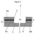
本発明の一態様においては、当該の方法では図1に示した装置が提供される。この装置は、その中に形成されたレセプタクル10を有するストリップSを含む。ストリップSは、任意の形状または大きさを有することができる。この態様におけるレセプタクルは、ベース1、壁2、および第1開口部3を有している。但し留意すべきことは、本発明によりカバーされる装置には、レセプタクルが異なる形状を有するもの、例えば形状が円錐、円錐台、または溝形のものがある。装置は電気化学セルを含み、電気化学セルの作用電極4は、レセプタクルの壁2に位置している。また装置は、任意の所望の位置にあることができる擬似参照電極も含む。擬似参照電極は図1に示していない。個別の対向電極を設けてもよい。
In one aspect of the invention, the method provides the apparatus shown in FIG. The apparatus includes a strip S having a
本発明の方法は、2つの絶縁層La、Lb間に作用電極層を含む積層体Lを最初に形成することによって装置を製造する工程を含む。必要に応じて追加の層を積層体に含めることができる。例えば作用電極層を層LaまたはLbに、通常は層Laの上に印刷することによって積層体を形成することができる。 The method of the present invention includes the step of manufacturing the device by first forming a laminate L including a working electrode layer between two insulating layers La, Lb. Additional layers can be included in the stack as needed. For example, the laminate can be formed by printing the working electrode layer on the layer La or Lb, usually on the layer La.
作業電極は、好ましくは炭素、パラジウム、金、白金、銅、または銀から、例えば炭素、パラジウム、金、または白金から、特に炭素から、例えば導電性インクの形で形成される。導電性インクは、追加素材、例えば白金および/または黒鉛を含有する改質インクであってもよい。 The working electrode is preferably formed from carbon, palladium, gold, platinum, copper or silver, for example from carbon, palladium, gold or platinum, in particular from carbon, for example in the form of a conductive ink. The conductive ink may be a modified ink containing additional materials such as platinum and / or graphite.
このインクは、通常、スクリーン印刷、インクジェット印刷、熱転写印刷、リソグラフ印刷、またはグラビア印刷技術、例えば国際公開公報第02/076160号(その内容が全体として参照により本明細書に組み入れられる)に記載された技術を利用して絶縁材La、Lbに印刷される。必要に応じて、同じまたは異なる材料からなる2つ以上のコーティングを塗布することができる。作用電極層の厚さは、通常0.01〜25μm、好ましくは0.05〜15μm、例えば0.1〜20μm、より好ましくは0.1〜10μmである。例えば厚さが0.1〜50μm、好ましくは5〜20μmの、より厚い作用電極層も考えられる。 This ink is typically described in screen printing, ink jet printing, thermal transfer printing, lithographic printing, or gravure printing techniques such as WO 02/076160, the contents of which are hereby incorporated by reference in their entirety. It is printed on the insulating materials La and Lb by using the above technique. If desired, two or more coatings of the same or different materials can be applied. The thickness of the working electrode layer is usually 0.01 to 25 μm, preferably 0.05 to 15 μm, for example 0.1 to 20 μm, more preferably 0.1 to 10 μm. For example, thicker working electrode layers with a thickness of 0.1 to 50 μm, preferably 5 to 20 μm are also conceivable.
層LaまたはLbへの作用電極の印刷は通常、選択されたパターンで実施される。選択されるパターンは、穴またはウェルの作製時に作用電極層の少なくとも一部が露出されることを保証するようなパターンである。また、導電トラックも都合よく絶縁層LaまたはLbに印刷される。導電トラックは、ポテンショスタットなど任意の必要な機器に作用電極を接続する。導電トラックは、作用電極自体に用いられる材料など任意の適切な導電性材料により作製することができる。 Printing of the working electrode on the layer La or Lb is usually carried out in a selected pattern. The pattern chosen is such that it ensures that at least a portion of the working electrode layer is exposed during the creation of the hole or well. Conductive tracks are also conveniently printed on the insulating layer La or Lb. The conductive track connects the working electrode to any necessary equipment such as a potentiostat. The conductive track can be made of any suitable conductive material, such as the material used for the working electrode itself.
第2絶縁層(通常は層Lb)は、絶縁材を作用電極層に印刷することによって形成することができる。絶縁層を形成するためのその他の技術としては、絶縁材溶液の溶媒蒸発法や、架橋結合による絶縁ポリマーの形成などが挙げられる。または、絶縁材の層を作用電極層に積層すること、例えば熱によって積層することによって絶縁層を形成してもよい。 The second insulating layer (usually layer Lb) can be formed by printing an insulating material on the working electrode layer. Other techniques for forming the insulating layer include solvent evaporation of an insulating material solution and formation of an insulating polymer by cross-linking. Alternatively, the insulating layer may be formed by laminating a layer of an insulating material on the working electrode layer, for example, by laminating by heat.
絶縁層La、Lbは通常、ポリマー、例えばアクリレート、ポリウレタン、PET、ポリオレフィン、ポリエステル、PVC、またはその他の任意の適切な絶縁材からなる。一態様においては、ポリマーはアクリレート、ポリウレタン、PET、ポリオレフィン、またはポリエステルである。ポリカーボネートおよびその他のプラスチックならびにセラミックも適切な絶縁材である。 The insulating layers La, Lb are typically made of a polymer, such as acrylate, polyurethane, PET, polyolefin, polyester, PVC, or any other suitable insulating material. In one aspect, the polymer is an acrylate, polyurethane, PET, polyolefin, or polyester. Polycarbonate and other plastics and ceramics are also suitable insulating materials.
図1に示した態様においては、このように形成される積層体Lは通常、50〜1000μm、好ましくは200〜800μm、例えば300〜600μmの深さ(すなわち、層Laの表面から層Lbの表面まで積層体の諸層を横切る距離および穴の作製される長さ)を有している。 In the embodiment shown in FIG. 1, the laminate L formed in this manner is usually 50 to 1000 μm, preferably 200 to 800 μm, for example, 300 to 600 μm deep (that is, the surface of the layer La to the surface of the layer Lb). The distance across the layers of the laminate and the length of the holes made).
次に、穴またはウェルが、積層体Lに作製される。穴は、積層体を完全に貫通する。したがって、レセプタクルを形成するために、通常はさらなる基板を積層体に取り付ける必要がある。但し、図3を参照して後述する一部の態様においては、さらなる基板を別個に取り付けることを避けることができる。これに反し、ウェルは積層体を完全には貫通せず、積層体に凹みまたはウェルを作製するものであり、これは、別個の基板を追加することなくレセプタクルが積層体に直接形成されるようにするものである。どちらの場合にも、作用電極層の端が露出されるように穴またはウェルが作用電極層を完全に貫通することが望ましい。図1に示した態様においては、穴が積層体を貫通して作製されている。 Next, holes or wells are created in the laminate L. The hole completely penetrates the stack. Therefore, it is usually necessary to attach an additional substrate to the stack to form the receptacle. However, in some embodiments described below with reference to FIG. 3, it is possible to avoid attaching additional substrates separately. On the other hand, the well does not completely penetrate the stack, creating a recess or well in the stack, so that the receptacle is formed directly in the stack without adding a separate substrate. It is to make. In either case, it is desirable for the hole or well to completely penetrate the working electrode layer so that the edges of the working electrode layer are exposed. In the embodiment shown in FIG. 1, the holes are made through the laminate.
穴またはウェルの作製には、レーザー穴あけ加工工程が含まれる。レーザー穴あけ加工工程によって積層体に穴またはウェルが作製されるように、レーザー穴あけ加工を単独で用いてもよい。または、レーザー穴あけ加工と別の技術、例えば機械技術を組み合わせて用いてもよい。例えば、中央プラグを取り囲む実質的に環状の穴またはウェルを作製すべく、積層体においてリングのレーザ穴あけ加工することによって(すなわち、トレパニング法によって)、穴またはウェルのエッジを形成するために、レーザー穴あけ加工を用いてもよい。中央プラグは別個に取り除くことができる。機械的打ち抜き工程を用いて中央プラグを取り除いてもよい。この態様においては、レーザー穴あけ加工工程を用いて穴またはウェルのエッジ、すなわちレセプタクルまたは部分レセプタクルの壁を形成する部分が形成される。この態様の好ましい様相においては、レーザー穴あけ加工工程では、積層体の一部のみ貫通される(すなわち、環状のウェルが形成される)のであって、積層体の残りの部分を切り通すには機械打ち抜きが用いられる。レーザー穴あけ加工工程では、通常、少なくとも上方の絶縁層Lbおよび作用電極層を貫通して穴あけが行われる。 The production of holes or wells includes a laser drilling process. Laser drilling may be used alone so that holes or wells are created in the laminate by the laser drilling process. Or you may use combining a laser drilling process and another technique, for example, a mechanical technique. For example, to form a hole or well edge by laser drilling a ring in the stack (ie, by trepanning) to create a substantially annular hole or well surrounding the central plug Drilling may be used. The central plug can be removed separately. The central plug may be removed using a mechanical stamping process. In this embodiment, a laser drilling process is used to form the edge of the hole or well, i.e. the part that forms the wall of the receptacle or partial receptacle. In a preferred aspect of this embodiment, in the laser drilling process, only a portion of the stack is penetrated (ie, an annular well is formed) and the machine is used to cut through the remaining portion of the stack. Punching is used. In the laser drilling process, drilling is usually performed through at least the upper insulating layer Lb and the working electrode layer.
または、穴またはウェルを機械的に打ち抜いて、穴またはウェルのエッジをレーザー穴あけ加工によって拡大することができる。レーザー穴あけ加工工程によって、穴またはウェルの壁表面を効果的に清浄化されるように、例えば少量の材料のみ取り除くことができる。この態様においては、レーザー穴あけ加工工程を用いて穴またはウェルのエッジ、すなわちレセプタクルまたは部分レセプタクルの壁を形成する部分が形成される。 Alternatively, the hole or well can be mechanically punched and the edge of the hole or well expanded by laser drilling. For example, only a small amount of material can be removed so that the laser drilling process effectively cleans the wall surface of the hole or well. In this embodiment, a laser drilling process is used to form the edge of the hole or well, i.e. the part that forms the wall of the receptacle or partial receptacle.
トレパニング技術を用いて穴またはウェルを形成する場合、トレパニング速度(T)およびレーザーのパルス繰り返し周波数(prf)が、T(rpm)/prf(kHz)>200という関係、好ましくはT(rpm)/prf(kHz)>250という関係を満たすことが好ましい。この関係が満たされた場合、得られる電気化学セルがより正確且つ一貫した結果をもたらすことが判明している。任意の特定理論によって拘束されることは望まないが、このように結果が向上した原因は、ビームパルスの重複が低減されるため、加熱によって誘発される試料の損傷が少なくなるためである。したがって、レーザーパラメータを慎重に選択することによって、そのような加熱効果を制御できること、そして、Tとprfの関係はこの有益な効果の達成手法の一例にすぎないことは、当業者にとって明らかである。 When forming holes or wells using trepanning techniques, the relationship between trepanning speed (T) and laser pulse repetition frequency (prf) is T (rpm) / prf (kHz)> 200, preferably T (rpm) / It is preferable to satisfy the relationship of prf (kHz)> 250. It has been found that when this relationship is satisfied, the resulting electrochemical cell provides more accurate and consistent results. While not wishing to be bound by any particular theory, the reason for this improved result is that the overlapping of the beam pulses is reduced, so less sample damage is induced by heating. Thus, it will be apparent to those skilled in the art that such heating effects can be controlled by careful selection of laser parameters, and that the relationship between T and prf is just one example of how to achieve this beneficial effect. .
レーザー穴あけ加工は、任意の適切なレーザードリル装置を用いて実施することができる。紫外線波長(例えば50〜400nm)、可視光波長(例えば、400〜700nm)、または赤外線波長(例えば700nm〜10μm、特に700nm〜5μmの近赤外領域)で動作するレーザーを用いることができる。適切な波長には、例えば100〜400nm、例えば150〜400nmが含まれる。パルスレーザーまたは連続波レーザーを用いることができる。パルスレーザーを用いる場合、好ましいパルス幅は0.1ps〜1000nsである。例えば、パルス幅は0.1ps〜1000psであってもよい。または、パルス幅は0.1ns〜1000ns、例えば1ns〜100nsであってもよい。このパルス幅を採用したレーザーを用いて製造された電気化学セルは、より正確であり、低い変動係数を有する結果をもたらすことが判明している。 Laser drilling can be performed using any suitable laser drilling device. A laser operating at an ultraviolet wavelength (for example, 50 to 400 nm), a visible light wavelength (for example, 400 to 700 nm), or an infrared wavelength (for example, a near infrared region of 700 nm to 10 μm, particularly 700 nm to 5 μm) can be used. Suitable wavelengths include, for example, 100-400 nm, such as 150-400 nm. A pulsed laser or continuous wave laser can be used. When a pulse laser is used, a preferable pulse width is 0.1 ps to 1000 ns. For example, the pulse width may be 0.1 ps to 1000 ps. Alternatively, the pulse width may be 0.1 ns to 1000 ns, for example, 1 ns to 100 ns. It has been found that electrochemical cells manufactured using lasers employing this pulse width are more accurate and result in a lower coefficient of variation.
本発明の一態様においては、穴またはウェルはウォータージェットによりガイドされるレーザー、例えばシノヴァ社のレーザーマイクロジェット技術を用いて形成される。 In one embodiment of the invention, the holes or wells are formed using a laser guided by a water jet, such as the laser microjet technology from Synova.
適切なレーザーの例には、それぞれ紫外線領域および/または可視光領域で動作するエキシマレーザー、窒素レーザー、ヘリウムカドミウムレーザー、およびイオンレーザーが含まれる。赤外線領域および/または可視光領域で動作するヘリウムネオンレーザーおよびCO2レーザーを用いることもできる。別のレーザーには、半導体レーザーおよび固体レーザー、例えばYAGレーザーおよびバナデイトレーザーが含まれる。レーザーの好ましい例には、エキシマレーザー、バナデイトレーザー、およびYAGレーザー、例えば倍数(二倍、三倍、および四倍を含む)周波数のバナデイトレーザーまたはYAGレーザーが含まれる。 Examples of suitable lasers include excimer lasers, nitrogen lasers, helium cadmium lasers, and ion lasers that operate in the ultraviolet and / or visible light region, respectively. It can also be used helium-neon laser and CO 2 laser operating in the infrared region and / or visible light region. Other lasers include semiconductor lasers and solid state lasers such as YAG lasers and vanadate lasers. Preferred examples of lasers include excimer lasers, vanadate lasers, and YAG lasers such as vanadate lasers or YAG lasers with multiple (including double, triple, and quadruple) frequencies.
本発明の一態様においては、一方または両方の絶縁層La、Lb(通常は少なくともLa)が、色素を含む。この色素は通常、レーザーの動作波長における絶縁層の吸収を高めるように選択される。このため、例えば紫外スペクトルで動作するレーザーの場合、紫外線を吸収する色素を層Laおよび/またはLbに含めることができる。この態様においては、レーザー波長における積層体Lの吸収度が大幅に向上し、その結果、レーザー穴あけ加工が容易になりその速度も速くなる。例えば、レーザー波長における積層体Lの吸収度が50%、75%、90%、または95%を上回ることがある。所望の波長において吸収する適切な色素は、当業者にとって公知である。 In one embodiment of the present invention, one or both of the insulating layers La and Lb (usually at least La) contains a dye. This dye is usually selected to enhance the absorption of the insulating layer at the operating wavelength of the laser. Thus, for example, in the case of a laser operating in the ultraviolet spectrum, a dye that absorbs ultraviolet light can be included in the layers La and / or Lb. In this aspect, the absorbance of the laminate L at the laser wavelength is greatly improved, and as a result, laser drilling is facilitated and the speed thereof is increased. For example, the absorbance of the laminate L at the laser wavelength may exceed 50%, 75%, 90%, or 95%. Suitable dyes that absorb at the desired wavelength are known to those skilled in the art.
本発明のさらなる態様においては、レーザー穴あけ加工はアシストガスの存在下で実施される。アシストガスを使用すると、レーザー切断において溶融物質を除去しやすくなるため、穴あけ加工速度が速くなる。反応性アシストガス、例えば酸素と、非反応性アシストガス、例えばアルゴンなどの不活性ガスの両方を使用することができる。 In a further aspect of the present invention, the laser drilling is performed in the presence of an assist gas. When the assist gas is used, it becomes easy to remove the molten material in the laser cutting, so that the drilling speed is increased. Both reactive assist gases, such as oxygen, and non-reactive assist gases, such as inert gases such as argon, can be used.
この態様の特定の局面においては、アシストガスとして酸素が用いられる。この局面においては、レーザーによって切断される表面が酸化され得る。作用電極表面の酸化は、それによって作用電極に機能性を導入できるようになるため、特に有利である。この技術は、例えば作用電極への触媒またはその他の電気活性材料の結合に利用することができる。 In a particular aspect of this embodiment, oxygen is used as the assist gas. In this aspect, the surface cut by the laser can be oxidized. Oxidation of the working electrode surface is particularly advantageous because it allows functionality to be introduced into the working electrode. This technique can be utilized, for example, for bonding a catalyst or other electroactive material to the working electrode.
本発明の別の態様においては、穴またはウェルの作製は、ウォータージェット切断工程または超音波切断工程を含む。ウォータージェット切断または超音波切断は単独で使用することもできるし、別の技術と組み合わせて、例えばレーザー穴あけ加工工程に関して上述した機械技術と組み合わせて使用することもできる。本技術分野で公知であり、μmまたはnmの寸法を有する穴またはウェルを形成するのに適した任意のウォータージェット切断装置または超音波切断装置を使用することができる。 In another aspect of the invention, the creation of the hole or well includes a water jet cutting process or an ultrasonic cutting process. Water jet cutting or ultrasonic cutting can be used alone or in combination with other techniques, for example, in combination with the mechanical techniques described above for the laser drilling process. Any water jet or ultrasonic cutting device known in the art and suitable for forming holes or wells having dimensions of μm or nm can be used.
通常、穴またはウェルは0.1〜5mm、例えば0.5〜2.0mm、または最大1.5mm、例えば1mmなどの幅を有する。この幅は、レセプタクルの断面の中点を横切って測定される壁間の最大距離と定義される。円筒形レセプタクルの場合、この幅は断面直径である。 Typically, the holes or wells have a width of 0.1-5 mm, such as 0.5-2.0 mm, or a maximum of 1.5 mm, such as 1 mm. This width is defined as the maximum distance between the walls measured across the midpoint of the cross section of the receptacle. In the case of a cylindrical receptacle, this width is the cross-sectional diameter.
穴またはウェルは、任意の所望の形状で形成することができる。適切な形状の例には、円筒形の穴またはウェル、及び、得られるレセプタクルまたは部分レセプタクルが円錐または円錐台の形状になるように傾斜した壁を有する穴またはウェルが含まれる。円錐形または円錐台形のウェルまたは穴の場合、前述の幅は、このように形成されるレセプタクルまたは部分レセプタクルの第1開口部の通常の幅である。または、穴またはウェルが溝の形のレセプタクルを提供してもよい。例えば、溝は約100〜約400μmの幅と、1〜10mm、例えば2〜5mmの長さを有することができる。 The holes or wells can be formed in any desired shape. Examples of suitable shapes include cylindrical holes or wells and holes or wells having walls that are slanted such that the resulting receptacle or partial receptacle is in the shape of a cone or frustoconical. In the case of a conical or frustoconical well or hole, the aforementioned width is the normal width of the first opening of the receptacle or partial receptacle thus formed. Alternatively, the hole or well may provide a receptacle in the form of a groove. For example, the grooves can have a width of about 100 to about 400 μm and a length of 1 to 10 mm, such as 2 to 5 mm.
穴またはウェルの作製によって作用電極が露出される。好ましくは、作用電極層が穴またはウェルの周囲全体にわたって露出されるような位置に穴またはウェルが形成される。この場合、最終的な装置における作用電極はレセプタクルまたは部分レセプタクルの周囲で連続した帯の形になる。好ましい態様においては、穴またはウェルの作製によって露出される作用電極はマイクロ電極である。さらなる好ましい態様においては、作用電極はマイクロバンド電極である。 The working electrode is exposed by creating a hole or well. Preferably, the hole or well is formed in a position such that the working electrode layer is exposed over the entire circumference of the hole or well. In this case, the working electrode in the final device is in the form of a continuous band around the receptacle or partial receptacle. In a preferred embodiment, the working electrode exposed by the creation of the hole or well is a microelectrode. In a further preferred embodiment, the working electrode is a microband electrode.
図1に示した態様においては、穴が形成されると、ベース、例えば絶縁材IMが積層体Lに取り付けられてレセプタクルのベース1が形成される。絶縁材IMは、例えば高分子シートを含む。適切なポリマーは、積層体Lの絶縁層を参照して説明したポリマーである。レセプタクルのベースを形成する表面に特定の特性を提供するために、ベースまたは絶縁材IMは表面処理が施されていてもよい。例えば、疎水性表面処理または親水性表面処理を用いてもよい。または、絶縁材IM自体を親水性多孔質膜または疎水性多孔質膜から形成してもよい。Pall filtration社のバーサポア膜(Versapor membrane)が、適切な絶縁材の例である。
In the embodiment shown in FIG. 1, when a hole is formed, a base, for example, an insulating material IM is attached to the laminate L to form a
積層体へのベースの接着は、任意の適切な技術によって実施することができる。例えば、加圧ローラーを用いて接着を実施することができる。感熱接着剤を用いてもよいが、その場合、高温が必要になる。感圧接着剤の場合は室温を用いることができる。 Adhesion of the base to the laminate can be performed by any suitable technique. For example, adhesion can be performed using a pressure roller. A heat sensitive adhesive may be used, but in that case, a high temperature is required. In the case of a pressure sensitive adhesive, room temperature can be used.
ベースの取り付けによってストリップSにレセプタクルが形成される。このように形成されたレセプタクルは通常、0.1〜5μl、例えば0.1〜3μlまたは0.2〜1μlの容積を有する。 A receptacle is formed on the strip S by attaching the base. The receptacle thus formed typically has a volume of 0.1-5 μl, for example 0.1-3 μl or 0.2-1 μl.
本発明の一態様においては、このように形成されたレセプタクルに電気活性物質が挿入される。電気活性物質は、試料に接触したときに電気化学反応を引き起こすことができる任意の物資である。したがって、試料がセルに挿入されて試料が電気活性物質に接触したとき、電気化学反応が発生し、セルにおいて測定可能な電流、電圧、および電荷が生じ得る。電気活性物質は、例えば電解触媒および/またはメディエーターを含んでいてもよい。適切な電解触媒は当業者にとって周知であり、様々な金属イオン(例えばコバルト)、および様々な酵素(例えば、乳酸オキシダーゼ、コレステロール脱水素酵素、グリセロール脱水素酵素、乳酸脱水素酵素、グリセロールキナーゼ、グリセロール−III−リン酸オキシダーゼ、およびコレステロールオキシダーゼ)が含まれる。適切なメディエーターの例は、フェリシアン化物/フェロシアン化物、およびルテニウム(III)ヘキサミン塩(例えば塩化物塩)などのルテニウム化合物である。 In one embodiment of the present invention, an electroactive substance is inserted into the thus formed receptacle. An electroactive substance is any material that can cause an electrochemical reaction when contacted with a sample. Thus, when the sample is inserted into the cell and the sample contacts the electroactive material, an electrochemical reaction can occur, resulting in measurable current, voltage, and charge in the cell. The electroactive material may include, for example, an electrocatalyst and / or a mediator. Suitable electrocatalysts are well known to those skilled in the art and include various metal ions (eg, cobalt) and various enzymes (eg, lactate oxidase, cholesterol dehydrogenase, glycerol dehydrogenase, lactate dehydrogenase, glycerol kinase, glycerol -III-phosphate oxidase and cholesterol oxidase). Examples of suitable mediators are ruthenium compounds such as ferricyanide / ferrocyanide and ruthenium (III) hexamine salts (eg chloride salts).
電気活性物質は、例えばマイクロピペット法または酵素ジェット印刷(enzyme jet printing)を用いてレセプタクルに挿入される。マイクロピペット法は一態様において、Allegro Technologies社のspot−on(商標)技術または類似の技術を用いて実施される。次に、任意の適切な技術、例えば空気乾燥、凍結乾燥、またはオーブンベーキングによって乾燥することができる。 The electroactive substance is inserted into the receptacle using, for example, a micropipette method or enzyme jet printing. The micropipette method, in one embodiment, is performed using Allegro Technologies' spot-on (TM) technology or similar technology. It can then be dried by any suitable technique, such as air drying, freeze drying, or oven baking.
好ましい態様においては、ウェルに1つ以上の通気口が形成される。これらの通気口があるため、試料がレセプタクルに入るときに、押しのけられる空気がレセプタクルから逃げることができる。通常は1つの通気口5がレセプタクルのベースに形成されるが、必要に応じて任意の数(例えば最大4つ)の穴があってもよい。通気口は、必要に応じてレセプタクルのベース以外の場所に位置決めしてもよい。通気口は、機械式穴あけ加工もしくは打ち抜き、またはレーザー穴あけ加工を含む任意の技術によって形成することができる。通気口は通常、毛管のような寸法を有している。例えば、通気口は約1〜600μm、例えば100〜500μmの直径を有し得る。レセプタクルに配置された液体試料が、表面張力が原因で通気口を通ってレセプタクルから出てしまうことが実質的に防止されるように、通気口は十分小さいことが望ましい。
In a preferred embodiment, one or more vents are formed in the well. Because of these vents, the displaced air can escape from the receptacle as the sample enters the receptacle. Normally, one
1つ以上の通気口は、積層体Lへのベースの取り付けの前後いずれにおいて形成してもよい。さらに、1つ以上の通気口は、レセプタクルへの電気活性物質の挿入の前後いずれにおいて形成してもよい。好ましい態様においては、電気活性物質がレセプタクルに挿入されて乾燥され、次に、レセプタクルのベースおよび乾燥された電気活性物質を貫通する通気口が形成される。このやり方では、通気口が電気活性物質で塞がれることがない。 One or more vent holes may be formed either before or after attachment of the base to the laminate L. Further, the one or more vents may be formed either before or after insertion of the electroactive material into the receptacle. In a preferred embodiment, the electroactive material is inserted into the receptacle and dried, and then a vent is formed through the base of the receptacle and the dried electroactive material. In this manner, the vent is not blocked by the electroactive material.
必要に応じて次に、浸透膜または半透膜を、レセプタクルを覆って配置してもよい。この膜は、被検試料が通過することができる材料からなることが好ましい。例えば試料が血漿である場合、血漿に対して透過性を有する膜であることが望ましい。膜として使用するのに適した材料には、ポリエステル、硝酸セルロース、ポリカーボネート、ポリスルホン、微孔ポリエーテルスルホンフィルム、PET、綿およびナイロン織物、被覆ガラス繊維、ならびにポリアクリロニトリル繊維が含まれる。場合により、使用に先立ってこれらの繊維に親水処理または疎水処理を施してもよい。必要に応じて、膜のその他の表面パラメータを変更することもできる。例えば、膜を通過する所望の試料の流れを促進するために、水における膜の接触角を変更する処理を用いてもよい。 An osmotic or semi-permeable membrane may then be placed over the receptacle as needed. This film is preferably made of a material through which the test sample can pass. For example, when the sample is plasma, a membrane that is permeable to plasma is desirable. Suitable materials for use as the membrane include polyester, cellulose nitrate, polycarbonate, polysulfone, microporous polyethersulfone film, PET, cotton and nylon fabrics, coated glass fibers, and polyacrylonitrile fibers. In some cases, these fibers may be subjected to a hydrophilic treatment or a hydrophobic treatment prior to use. Other surface parameters of the membrane can be changed as needed. For example, a process that changes the contact angle of the membrane in water may be used to facilitate the flow of the desired sample through the membrane.
膜は、それぞれが同じまたは異なる1つ、2つ、またはそれ以上の材料層を含むことができる。例えば、異なる機能を有する2つの異なる膜を用いることができる。例えば、2つの層の異なる膜材料を含む従来型の二重層膜を用いることができる。別の態様においては、膜は湿潤膜および血液ろ過膜を含む。ペテックス(Petex)が適切な湿潤膜であるが、好ましいろ過膜については後述する。一態様においては、膜はペテックス層およびPall BTS層を含む。 The membrane can include one, two, or more layers of material, each the same or different. For example, two different films with different functions can be used. For example, a conventional double layer film comprising two layers of different film materials can be used. In another embodiment, the membrane includes a wet membrane and a blood filtration membrane. Petex is a suitable wet membrane, but preferred filtration membranes are described below. In one aspect, the membrane includes a petex layer and a Pall BTS layer.
また、膜を用いて、セルに入ることが望ましくない一部の成分をろ過して取り除くこともできる。例えば、赤血球など一部の血液製剤を、これらの粒子がレセプタクルに入らないようにこの方法で分離することができる。血液ろ過膜を含め、適切なろ過膜は当技術分野で公知である。血液ろ過膜の例は、Pall filtration社のPresence 200、Whatman VF2、Whatman Cyclopore、Spectral NX、Spectral X、およびPall BTS、例えばPall filtration社のPresence 200、Whatman VF2、Whatman Cyclopore、Spectral NX、およびSpectral Xである。ガラス繊維フィルタ、例えばWhatman VF2は全血から血漿を分離することができ、全血検体が装置に供給され且つ被検試料が血漿である場合に使用するのに適している。血液からLDLを除去する活性膜を用いることもできる。
The membrane can also be used to filter out some components that are not desired to enter the cell. For example, some blood products such as red blood cells can be separated in this way so that these particles do not enter the receptacle. Suitable filtration membranes, including blood filtration membranes, are known in the art. Examples of blood filtration membranes include Pall Filtration's
膜は、通常、例えば両面接着剤またはスクリーン印刷感圧接着剤を用いてストリップの表面に取り付けられる。膜の取り付けは、例えば、レセプタクルを覆う領域、および通常はより広い作用領域を覆う領域における接着剤を除去するように打ち抜かれている感圧接着剤(流し込まれた)を用いて実施することができる。 The membrane is usually attached to the surface of the strip using, for example, a double-sided adhesive or a screen printing pressure sensitive adhesive. Membrane attachment may be performed, for example, using a pressure sensitive adhesive (poured) that has been punched to remove the adhesive in the area covering the receptacle and usually in the area covering the larger area of action. it can.
本発明の別の態様においては、ストリップSは部分レセプタクルを含む。この態様においては、部分レセプタクルは、第1開口部を第2開口部につなぐ1つ以上の壁2を含む。第2開口部を基板に対して配置してレセプタクルを形成することができるが、その際、基板がこのように形成されるレセプタクルの真のベースを形成する。これらの装置は、積層体Lに穴を形成することによって、但し積層体にベースを取り付ける工程を実施することなく、本発明の方法に従って製造することができる。
In another aspect of the invention, strip S includes a partial receptacle. In this aspect, the partial receptacle includes one or
後述の内容を除いて第1態様と同じである本発明のさらに別の態様を図2に示している。この態様においては、方法は、積層体Lにおいてウェルを形成する工程を含む。このため、レーザー穴あけ加工工程は、通常、所望のレセプタクル10の寸法および容積を有するウェルを積層体Lに直接形成する工程を含む。これにより、ベースを積層体に取り付ける追加工程が避けられる。この場合、ストリップは積層体Lのみからなることができる。
FIG. 2 shows still another aspect of the present invention which is the same as the first aspect except for the contents described below. In this embodiment, the method includes a step of forming a well in the stacked body L. For this reason, the laser drilling process usually includes a process of directly forming a well having a desired size and volume of the
この態様においては、積層体Lは通常、少なくとも1mm、例えば少なくとも1.5mmまたは少なくとも2mmの厚さを有する。積層体に形成されるウェルは通常、50〜1000μm、好ましくは200〜800μm、例えば300〜600μmの深さを有する。 In this embodiment, the laminate L typically has a thickness of at least 1 mm, such as at least 1.5 mm or at least 2 mm. The well formed in the laminate usually has a depth of 50 to 1000 μm, preferably 200 to 800 μm, for example 300 to 600 μm.
後述の内容を除いて第1態様と同じである本発明のさらに別の態様を図3に示している。この態様においては、穴の最も狭い部分が例えば600μm以下の幅を有するように、傾斜した壁を有する穴が積層体に形成される。穴の最も狭い部分の好ましい幅は1〜600μm、例えば100〜500μmである。穴の最も狭い部分の幅は、最も狭い地点における穴の断面の中間点を横切って測定される壁間の距離と定義される。 FIG. 3 shows still another aspect of the present invention which is the same as the first aspect except for the contents described below. In this aspect, the hole having an inclined wall is formed in the laminate so that the narrowest part of the hole has a width of, for example, 600 μm or less. The preferred width of the narrowest part of the hole is 1 to 600 μm, for example 100 to 500 μm. The width of the narrowest part of the hole is defined as the distance between the walls measured across the midpoint of the cross section of the hole at the narrowest point.
この態様においては一般に、穴は、第1開口部3から離れるにしたがって徐々に狭くなる幅を有する円錐台形の穴である。穴の幅は、穴が通気口5として機能できようにベースにおいて十分狭くなっている。このため、ベースを積層体に取り付ける追加工程および通気口を形成する工程を避けることができる。
In general, in this embodiment, the hole is a frustoconical hole having a width that gradually decreases as the distance from the
上記のようにストリップが2つ以上のレセプタクルまたは部分レセプタクルを含む装置を、本発明の方法によって製造することもできる。これは、作用電極層の適切なパターンを絶縁層La、Lbに印刷し、2つ以上の穴またはウェルを積層体Lに形成することによって達成される。それぞれの穴またはウェルが上記のように形成されることが好ましい。 An apparatus in which the strip includes two or more receptacles or partial receptacles as described above can also be manufactured by the method of the present invention. This is accomplished by printing a suitable pattern of working electrode layers on the insulating layers La, Lb and forming two or more holes or wells in the stack L. Each hole or well is preferably formed as described above.
本発明に従って製造された装置は、被検試料を1つのまたは各レセプタクルに挿入し、作用電極と対向電極間に電位を印加し、その結果生じる電気化学応答を測定する電気化学検出方法で用いることができる。例えば、生じる電流を測定することができる。このように、水、ビール、ワイン、血液、もしくは尿の試料、またはその他の生体液もしくは非生体液の試料における様々な物質の含有量を求めるために装置を用いることができる。例えば、環境アセスメント用の試料のペンタクロロフェノール含有量を求めたり、心臓のリスク分析で使用するためにコレステロール、HDL、LDL、およびトリグリセリドのレベルを測定したり、例えば糖尿病患者が使用するために血糖値を測定するために、この装置を用いることができる。本発明の装置の適切な用途のさらなる例は、腎臓病に罹患した患者の状態を測定するための腎機能モニターである。この場合、この装置を用いて、尿におけるクレアチニン、尿素、カリウム、およびナトリウムのレベルをモニターすることができる。この装置を用いて、虚血または血漿の試料を識別することもできる。
実施例
The apparatus manufactured according to the present invention is used in an electrochemical detection method in which a test sample is inserted into one or each receptacle, a potential is applied between the working electrode and the counter electrode, and the resulting electrochemical response is measured. Can do. For example, the resulting current can be measured. Thus, the apparatus can be used to determine the content of various substances in water, beer, wine, blood, or urine samples, or other biological or non-biological fluid samples. For example, determining the pentachlorophenol content of a sample for environmental assessment, measuring cholesterol, HDL, LDL, and triglyceride levels for use in cardiac risk analysis, or blood glucose for use by, for example, diabetics This device can be used to measure values. A further example of a suitable application of the device of the present invention is a renal function monitor for measuring the status of patients suffering from kidney disease. In this case, the device can be used to monitor creatinine, urea, potassium, and sodium levels in the urine. This device can also be used to identify ischemic or plasma samples.
Example
本発明に従って製造された装置がより高い信頼性を有していることを実証するために、本発明者らは、本発明の各種装置を用いて、および積層体に穴を形成する機械的打ち抜きを用いて製造された装置を用いて得られた結果の一貫性を比較するという試験を実施した。下記のすべての電圧は標準水素電極に対するものであり、IUPAC命名法を用いている。 In order to demonstrate that the device manufactured according to the present invention is more reliable, the inventors have used the various devices of the present invention and mechanical punching to form holes in the laminate. A test was performed to compare the consistency of the results obtained with an apparatus manufactured using All voltages below are relative to a standard hydrogen electrode and use the IUPAC nomenclature.
実施例1
図1に示した種類の4つのレセプタクルを有する装置を用いて、すべての試験を実施した。
Example 1
All tests were performed using a device having four receptacles of the type shown in FIG.
ヒートシールを用いて250μm PETのフィルムを被覆した。次に、作用電極および導電トラックを画定するパターンに導電性カーボンインクを用いて、ヒートシール被覆の裏面に、このフィルムは印刷された。次に、これを100℃で1時間乾燥した。続いて、誘電体インクを用いてカーボンインク印刷にオーバープリントを実施した。但し、測定装置のコネクタと結合するために必要なトラック部分にはオーバープリントを実施しなかった。次に、誘電体インクを100℃で2分間乾燥した。誘電体インクの被覆をさらに施し、それを100℃で1時間乾燥した。 A 250 μm PET film was coated using heat sealing. The film was then printed on the back side of the heat seal coating using conductive carbon ink in a pattern defining working electrodes and conductive tracks. Next, this was dried at 100 ° C. for 1 hour. Subsequently, carbon ink printing was overprinted using dielectric ink. However, overprinting was not performed on the track portion necessary for coupling with the connector of the measuring apparatus. Next, the dielectric ink was dried at 100 ° C. for 2 minutes. A further coating of dielectric ink was applied and it was dried at 100 ° C. for 1 hour.
次に、266nmで動作する周波数4倍Nd YAGレーザーを用いたレーザー穴あけ加工によって、1mmの直径を有する4つの穴をフィルムに形成した。次に、フィルムのヒートシールで被覆された面を加熱によって125μm PETのベースフィルムに貼り合わせて、4つのウェルを形成した。この加熱工程中に、ヒートシールがベースフィルムに接着された。Ag/AgCl擬似参照電極を用いた。周波数4倍Nd YAGレーザーを用いて、直径250μmの通気口を各ウェルのベースに形成した。 Next, four holes having a diameter of 1 mm were formed in the film by laser drilling using a 4 × frequency Nd YAG laser operating at 266 nm. Next, the surface covered with the heat seal of the film was bonded to a base film of 125 μm PET by heating to form four wells. During this heating step, a heat seal was adhered to the base film. An Ag / AgCl pseudo reference electrode was used. Using a quadruple frequency Nd YAG laser, a 250 μm diameter vent was formed in the base of each well.
次に、約4.0mMのRu(NH3)6Cl3水溶液に、上記のように製造された5つの装置を浸した。−0.45Vの電位を各セルに同時に印加し、1秒後に各セルの電流を順次測定した。その結果、合計で20の測定値が得られた。 Next, the five devices prepared as described above were immersed in about 4.0 mM Ru (NH 3 ) 6 Cl 3 aqueous solution. A potential of −0.45 V was simultaneously applied to each cell, and the current of each cell was measured sequentially after 1 second. As a result, a total of 20 measured values were obtained.
約8.0mMのRu(NH3)6Cl3溶液を用いて、この実験を繰り返した。両方の実験結果を図4に示している(四角で示した点、上側の線)。 This experiment was repeated with approximately 8.0 mM Ru (NH 3 ) 6 Cl 3 solution. The results of both experiments are shown in FIG. 4 (dots indicated by squares, upper line).
実施例2
レーザー穴あけ加工ではなく1mmのスチールパンチとダイのセットを用いてフィルムの穴を開けたことを除き、実施例1に記載の方法に従って装置を製造した。また、機械的穿孔によって通気口を形成した。
Example 2
An apparatus was manufactured according to the method described in Example 1 except that the film was punched using a 1 mm steel punch and die set instead of laser drilling. In addition, vents were formed by mechanical drilling.
約4.0及び約8.0mMのRu(NH3)6Cl3を含有する水溶液を、実施例1に記載の技術に従ってこれらの装置を用いて試験した。その結果を図4に示している(円で示した点、下側の線)。 Aqueous solutions containing about 4.0 and about 8.0 mM Ru (NH 3 ) 6 Cl 3 were tested using these devices according to the technique described in Example 1. The result is shown in FIG. 4 (dots indicated by circles, lower line).
図4は、レーザー穴あけ加工で設けられたウェルを用いて試験した各試料について、測定された電流の高い一貫性が得られたことを示している。測定された電流の分布において、レーザー穴あけ加工で設けられたウェルの場合、4.0mMでCV=3.2%、8.0mMでCV=2.9%(平均CV=3.0%)という結果が得られたが、機械的に打ち抜かれたウェルの場合、4.0mMでCV=9.7%、8.0mMでCV=15.5%(平均CV=12.6%)という結果が得られた。mM単位のRu(NH3)6Cl3濃度の測定値に変換すると、レーザー加工で設けられたウェルの場合、4.0mMでCV=3.9%、8.0mMでCV=3.2%(平均CV=3.6%)という結果が得られたが、打ち抜かれたウェルの場合、4.0mMでCV=11.6%、8.0mMでCV=17.0%(平均CV=14.3%)という結果が得られた。 FIG. 4 shows that a high consistency of the measured current was obtained for each sample tested using wells provided by laser drilling. In the measured current distribution, in the case of a well provided by laser drilling, CV = 3.2% at 4.0 mM, CV = 2.9% at 8.0 mM (average CV = 3.0%) Results were obtained, but in the case of wells that were mechanically punched, CV = 9.7% at 4.0 mM and CV = 15.5% at 8.0 mM (average CV = 12.6%). Obtained. When converted to measured values of Ru (NH 3 ) 6 Cl 3 concentration in mM units, CV = 3.9% at 4.0 mM and CV = 3.2% at 8.0 mM for wells provided by laser processing. Results were obtained (average CV = 3.6%), but in the case of punched wells, 4.0 mM at CV = 11.6%, 8.0 mM at CV = 17.0% (average CV = 14 .3%) was obtained.
実施例3
通気口の穴あけ加工および拡散膜の取り付けに先立って、コレステロールエステラーゼおよびコレステロール脱水素酵素を含む電気活性物質を、このように形成されたウェルに入れたことを除き、実施例1に記載の方法に従って装置を製造した。次に、この物質を凍結乾燥した。
Example 3
Prior to vent hole drilling and diffusion membrane attachment, an electroactive substance comprising cholesterol esterase and cholesterol dehydrogenase was placed in the well formed thus, according to the method described in Example 1. The device was manufactured. This material was then lyophilized.
次に、約3.3mMの総コレステロールを含有する血漿は、上記のように製造した4つの装置に適用され、60秒の湿潤時間により、凍結乾燥された電気活性物質が血漿内で再懸濁できるようにした。+0.15Vの酸化電位を各セルに同時に印加し、1秒後、各ウェルについて電流測定法により電流を順次測定し、合計で16の結果が得られた。これらの結果を図5に記録している。 Next, plasma containing about 3.3 mM total cholesterol is applied to the four devices prepared as described above, with 60 seconds of wet time allowing the lyophilized electroactive substance to be resuspended in the plasma. I was able to do it. An oxidation potential of +0.15 V was simultaneously applied to each cell, and after 1 second, current was sequentially measured for each well by a current measurement method, and a total of 16 results were obtained. These results are recorded in FIG.
約6.03mMの総コレステロール量を有する血漿を用いて実験を繰り返し、その結果も図5に記録している。 The experiment was repeated with plasma having a total cholesterol level of about 6.03 mM, and the results are also recorded in FIG.
図5は、高い一貫性の結果が得られたことを示している。測定された電流の分布において、3.3mMの総コレステロール量試料ではCV=6.1%、あるいはmM単位の総コレステロール濃度に変換した場合はCV=6.2%という結果が得られた。測定された電流の分布において、6.03mMの総コレステロール量試料ではCV=9.0%、あるいはmM単位の総コレステロール濃度に変換した場合はCV=9.2%という結果が得られた。平均値はCV=7.6%(電流)およびCV=7.7%(濃度)であった。 FIG. 5 shows that a highly consistent result was obtained. In the measured current distribution, the result was CV = 6.1% for the 3.3 mM total cholesterol sample, or CV = 6.2% when converted to a total cholesterol concentration in mM units. In the measured current distribution, the result was CV = 9.0% for the total amount of cholesterol of 6.03 mM, or CV = 9.2% when converted to the total cholesterol concentration in mM units. The average values were CV = 7.6% (current) and CV = 7.7% (concentration).
実施例4
図1に示した種類の4つのレセプタクルを有する装置を用いて、すべての試験を実施した。
Example 4
All tests were performed using a device having four receptacles of the type shown in FIG.
作用電極および導電トラックを画定するパターンにおいて導電性カーボンインクを用いて、250μm PETのフィルムは印刷された。次に、これを100℃で1時間乾燥した。続いて、カーボンインク印刷を誘電体インクでオーバープリントを実施した。但し、測定装置のコネクタと結合するために必要なトラック部分にはオーバープリントを実施しなかった。次に、誘電体インクを100℃で2分間乾燥した。誘電体インクの2つの被覆をさらに施し、それを100℃で1時間乾燥した。 A film of 250 μm PET was printed using conductive carbon ink in a pattern defining the working electrode and conductive track. Next, this was dried at 100 ° C. for 1 hour. Subsequently, carbon ink printing was overprinted with dielectric ink. However, overprinting was not performed on the track portion necessary for coupling with the connector of the measuring apparatus. Next, the dielectric ink was dried at 100 ° C. for 2 minutes. Two further coatings of dielectric ink were applied and it was dried at 100 ° C. for 1 hour.
次に、266nmの波長、2kHzのパルス繰り返し周波数(prf)、および450rpmのトレパニング速度で動作するNd:YVO4パルスレーザーを用いて、1mmの直径を有する4つの穴をレーザー穴あけ加工によってフィルムに形成した。次に、粘着テープを用いてPall社のバーサポア多孔質膜の基層にフィルムを接着させて、4つのウェルを形成した。Ag/AgCl擬似参照電極を用いた。 Next, four holes with a diameter of 1 mm are formed in the film by laser drilling using a Nd: YVO 4 pulse laser operating at a wavelength of 266 nm, a pulse repetition frequency (prf) of 2 kHz, and a trepanning speed of 450 rpm. did. Next, the film was adhered to the base layer of the Pall Versapore porous membrane using an adhesive tape to form four wells. An Ag / AgCl pseudo reference electrode was used.
次に、約5.0mMのRu(NH3)6Cl3水溶液は、上記のように製造された5つの装置に適用された。電位の印加に先立って、5秒の期間を経過させた。−0.45Vの電位を各セルに同時に印加し、1秒後に各セルの電流を順次測定した。その結果、合計で20の測定値が得られた。約10.0mMのRu(NH3)6Cl3溶液を用いて実験を繰り返し、合計で40の測定値が得られた。 Next, approximately 5.0 mM Ru (NH 3 ) 6 Cl 3 aqueous solution was applied to the five devices produced as described above. Prior to application of the potential, a period of 5 seconds was allowed to elapse. A potential of −0.45 V was simultaneously applied to each cell, and the current of each cell was measured sequentially after 1 second. As a result, a total of 20 measured values were obtained. The experiment was repeated with approximately 10.0 mM Ru (NH 3 ) 6 Cl 3 solution, for a total of 40 measurements.
下記の表1に示した様々なレーザー動作条件を用いて製造された装置を用いて、この一連の実験を繰り返した。一連の40の結果それぞれについて、変動係数(CV)を求めた。図6は、トレパニング速度/prfの比率と得られたCV値の関係を示している。 This series of experiments was repeated using equipment manufactured using the various laser operating conditions shown in Table 1 below. The coefficient of variation (CV) was determined for each of a series of 40 results. FIG. 6 shows the relationship between the ratio of trepanning speed / prf and the obtained CV value.
図6は、トレパニング速度(rpm)/prf(kHz)の比率が200を超える場合、特に250を超える場合、得られた結果の高い一貫性を実証している。 FIG. 6 demonstrates the high consistency of the results obtained when the ratio of trepanning speed (rpm) / prf (kHz) exceeds 200, in particular when it exceeds 250.

様々な特定の態様を参照して本発明について説明してきた。但し、当然のことながら、本発明はこれらの特定の態様に限定されるものではない。 The invention has been described with reference to various specific aspects. However, it should be understood that the present invention is not limited to these specific embodiments.
Claims (20)
前記方法が、
− 2つの絶縁層間に作用電極層を有する積層体を形成する工程と、
− 作用電極層を貫通する穴またはウェルを積層体に作製する工程と、
− 場合により、積層体をベースに取り付けてレセプタクルを形成する工程を含み、
前記の穴またはウェルを形成する工程が、積層体をレーザー穴あけ加工する工程を含む、方法。 A method of manufacturing a device having an electrochemical cell, the device comprising a strip containing a receptacle or partial receptacle formed therein, the working electrode of the electrochemical cell being located on the wall of the receptacle or partial receptacle And
The method comprises
-Forming a laminate having a working electrode layer between two insulating layers;
-Creating a hole or well in the stack through the working electrode layer;
-Optionally including attaching the laminate to the base to form a receptacle;
The method of forming the hole or well includes a step of laser drilling the laminate.
前記方法が、
− 2つの絶縁層間に作用電極層を含む積層体を形成する工程と、
− 作用電極層を貫通する穴またはウェルを積層体に作製する工程と、
− 場合により、該積層体をベースに取り付けてレセプタクルを形成する工程を含み、
穴またはウェルを形成する工程が、ウォータージェット切断または超音波切断によって積層体を切断する工程を含む、請求項1の方法の改良。 The method of claim 1, wherein the device comprises a strip having a receptacle or partial receptacle formed therein, the wall of the receptacle or partial receptacle being a method of manufacturing a device having an electrochemical cell. The working electrode of the electrochemical cell is located in
The method comprises
-Forming a laminate comprising a working electrode layer between two insulating layers;
-Creating a hole or well in the stack through the working electrode layer;
-Optionally, attaching the laminate to a base to form a receptacle;
The method improvement of claim 1 wherein the step of forming the hole or well comprises the step of cutting the laminate by water jet cutting or ultrasonic cutting.
− 電気化学セルの両端に電位を印加することと、
− その結果生じる電気化学応答を測定することを含む電気化学検出方法。 Inserting a sample into a receptacle or partial receptacle of the device according to claim 18 or 19;
-Applying a potential across the electrochemical cell;
An electrochemical detection method comprising measuring the resulting electrochemical response.
Applications Claiming Priority (3)
| Application Number | Priority Date | Filing Date | Title |
|---|---|---|---|
| GB0413244A GB0413244D0 (en) | 2004-06-14 | 2004-06-14 | Water-jet or ultra-sonic cutting manufacturing method |
| GB0413224A GB0413224D0 (en) | 2004-06-14 | 2004-06-14 | Laser manufacturing method |
| PCT/GB2005/002345 WO2005121762A1 (en) | 2004-06-14 | 2005-06-14 | Micro-band electrode manufacturing method |
Publications (2)
| Publication Number | Publication Date |
|---|---|
| JP2008502897A true JP2008502897A (en) | 2008-01-31 |
| JP2008502897A5 JP2008502897A5 (en) | 2008-06-19 |
Family
ID=34970603
Family Applications (1)
| Application Number | Title | Priority Date | Filing Date |
|---|---|---|---|
| JP2007516030A Withdrawn JP2008502897A (en) | 2004-06-14 | 2005-06-14 | Manufacturing method of microband electrode |
Country Status (4)
| Country | Link |
|---|---|
| US (1) | US20080116082A1 (en) |
| EP (1) | EP1756558A1 (en) |
| JP (1) | JP2008502897A (en) |
| WO (1) | WO2005121762A1 (en) |
Cited By (1)
| Publication number | Priority date | Publication date | Assignee | Title |
|---|---|---|---|---|
| JP2009241153A (en) * | 2008-03-28 | 2009-10-22 | Siemens Ag | Method for making hole |
Families Citing this family (8)
| Publication number | Priority date | Publication date | Assignee | Title |
|---|---|---|---|---|
| GB0414550D0 (en) * | 2004-06-29 | 2004-08-04 | Oxford Biosensors Ltd | Electrochemical sensing method |
| GB0414548D0 (en) | 2004-06-29 | 2004-08-04 | Oxford Biosensors Ltd | Electrode preconditioning |
| JP2008186870A (en) * | 2007-01-26 | 2008-08-14 | Disco Abrasive Syst Ltd | Method of machining via hole |
| US8134098B2 (en) * | 2007-09-28 | 2012-03-13 | Sugino Machine Limited | Laser machining apparatus using laser beam introduced into jet liquid column |
| EP2614364A1 (en) | 2010-09-10 | 2013-07-17 | Hitachi Chemical Co., Ltd. | Individually addressable band electrode arrays and methods to prepare the same |
| CN104364932B (en) * | 2012-05-31 | 2017-03-15 | 本田技研工业株式会社 | Power storage module and the fixture construction of power storage module |
| US11298059B2 (en) * | 2016-05-13 | 2022-04-12 | PercuSense, Inc. | Analyte sensor |
| CN111055011B (en) * | 2019-12-29 | 2020-09-29 | 中国科学院西安光学精密机械研究所 | High-coaxiality and large-depth-diameter-ratio micropore machining method |
Family Cites Families (11)
| Publication number | Priority date | Publication date | Assignee | Title |
|---|---|---|---|---|
| US5246576A (en) * | 1990-12-10 | 1993-09-21 | Ppg Industries, Inc. | Cathode in a layered circuit and electrochemical cell for a measurement of oxygen in fluids |
| EP0629867B1 (en) * | 1993-06-16 | 1999-01-27 | Nitto Denko Corporation | Probe structure |
| US5590460A (en) * | 1994-07-19 | 1997-01-07 | Tessera, Inc. | Method of making multilayer circuit |
| US6174420B1 (en) * | 1996-11-15 | 2001-01-16 | Usf Filtration And Separations Group, Inc. | Electrochemical cell |
| AU4902897A (en) * | 1996-11-08 | 1998-05-29 | W.L. Gore & Associates, Inc. | Method for improving reliability of thin circuit substrates by increasing the T of the substrate |
| US6274224B1 (en) * | 1999-02-01 | 2001-08-14 | 3M Innovative Properties Company | Passive electrical article, circuit articles thereof, and circuit articles comprising a passive electrical article |
| US6488829B1 (en) * | 1999-08-05 | 2002-12-03 | Essen Instruments Inc | High-throughput electrophysiological measurement apparatus |
| US20020090649A1 (en) * | 1999-12-15 | 2002-07-11 | Tony Chan | High density column and row addressable electrode arrays |
| WO2003046538A1 (en) * | 2001-11-26 | 2003-06-05 | Ischemia Technologies, Inc. | Electrochemical detection of ischemia |
| GB0130684D0 (en) * | 2001-12-21 | 2002-02-06 | Oxford Biosensors Ltd | Micro-band electrode |
| US20060008581A1 (en) * | 2004-07-09 | 2006-01-12 | Mark Hyland | Method of manufacturing an electrochemical sensor |
-
2005
- 2005-06-14 JP JP2007516030A patent/JP2008502897A/en not_active Withdrawn
- 2005-06-14 US US11/629,389 patent/US20080116082A1/en not_active Abandoned
- 2005-06-14 EP EP05751873A patent/EP1756558A1/en not_active Withdrawn
- 2005-06-14 WO PCT/GB2005/002345 patent/WO2005121762A1/en active Application Filing
Cited By (2)
| Publication number | Priority date | Publication date | Assignee | Title |
|---|---|---|---|---|
| JP2009241153A (en) * | 2008-03-28 | 2009-10-22 | Siemens Ag | Method for making hole |
| US9597751B2 (en) | 2008-03-28 | 2017-03-21 | Siemens Aktiengesellschaft | Method for producing a hole with side-delimiting flanks in a component |
Also Published As
| Publication number | Publication date |
|---|---|
| WO2005121762A1 (en) | 2005-12-22 |
| EP1756558A1 (en) | 2007-02-28 |
| US20080116082A1 (en) | 2008-05-22 |
Similar Documents
| Publication | Publication Date | Title |
|---|---|---|
| JP2008502897A (en) | Manufacturing method of microband electrode | |
| JP2008505337A (en) | Electrodes for electrochemical sensors | |
| AU2002367214B9 (en) | Micro-band electrode | |
| US9285335B2 (en) | Method for measuring blood components and biosensor and measuring instrument for use therein | |
| US7943022B2 (en) | Analyte test strip with improved reagent deposition | |
| EP1203956B1 (en) | Biosensor with flow channel | |
| DK170656B1 (en) | Enzyme electrode type sensor and method for determining an analyte in a sample | |
| US6679841B2 (en) | Fluid collection and monitoring device | |
| CN106353387B (en) | A kind of electrochemical test bar and the method for detecting a variety of determinands simultaneously | |
| US20060099107A1 (en) | Sensor | |
| US20050072670A1 (en) | Biosensor | |
| JP2009500601A (en) | Electrode preconditioning | |
| KR20010092723A (en) | Electrode strips for testing small volumes | |
| JP2008502897A5 (en) | ||
| EP2198283B1 (en) | Method of defining electrodes using laser-ablation and dielectric material | |
| JP2004325384A (en) | Biosensor | |
| JP2003254933A5 (en) | ||
| JP2006275716A (en) | Test paper |
Legal Events
| Date | Code | Title | Description |
|---|---|---|---|
| A521 | Written amendment |
Free format text: JAPANESE INTERMEDIATE CODE: A523 Effective date: 20080424 |
|
| A621 | Written request for application examination |
Free format text: JAPANESE INTERMEDIATE CODE: A621 Effective date: 20080424 |
|
| A977 | Report on retrieval |
Free format text: JAPANESE INTERMEDIATE CODE: A971007 Effective date: 20100823 |
|
| A761 | Written withdrawal of application |
Free format text: JAPANESE INTERMEDIATE CODE: A761 Effective date: 20101224 |
|
| A521 | Written amendment |
Free format text: JAPANESE INTERMEDIATE CODE: A523 Effective date: 20110107 |