JP2008500678A - Configurable ready / busy control - Google Patents
Configurable ready / busy control Download PDFInfo
- Publication number
- JP2008500678A JP2008500678A JP2007515201A JP2007515201A JP2008500678A JP 2008500678 A JP2008500678 A JP 2008500678A JP 2007515201 A JP2007515201 A JP 2007515201A JP 2007515201 A JP2007515201 A JP 2007515201A JP 2008500678 A JP2008500678 A JP 2008500678A
- Authority
- JP
- Japan
- Prior art keywords
- controller
- busy
- integrated circuit
- memory
- ready
- Prior art date
- Legal status (The legal status is an assumption and is not a legal conclusion. Google has not performed a legal analysis and makes no representation as to the accuracy of the status listed.)
- Pending
Links
Images


Classifications
-
- G—PHYSICS
- G06—COMPUTING; CALCULATING OR COUNTING
- G06F—ELECTRIC DIGITAL DATA PROCESSING
- G06F12/00—Accessing, addressing or allocating within memory systems or architectures
-
- G—PHYSICS
- G11—INFORMATION STORAGE
- G11C—STATIC STORES
- G11C16/00—Erasable programmable read-only memories
- G11C16/02—Erasable programmable read-only memories electrically programmable
- G11C16/06—Auxiliary circuits, e.g. for writing into memory
- G11C16/10—Programming or data input circuits
-
- G—PHYSICS
- G06—COMPUTING; CALCULATING OR COUNTING
- G06F—ELECTRIC DIGITAL DATA PROCESSING
- G06F13/00—Interconnection of, or transfer of information or other signals between, memories, input/output devices or central processing units
- G06F13/14—Handling requests for interconnection or transfer
- G06F13/16—Handling requests for interconnection or transfer for access to memory bus
Landscapes
- Engineering & Computer Science (AREA)
- Theoretical Computer Science (AREA)
- Physics & Mathematics (AREA)
- General Engineering & Computer Science (AREA)
- General Physics & Mathematics (AREA)
- Read Only Memory (AREA)
- Static Random-Access Memory (AREA)
- Memory System Of A Hierarchy Structure (AREA)
- Multi Processors (AREA)
Abstract
Description
本願は、集積回路に関し、特に1つ以上の信号線を介してコントローラと通信する不揮発性メモリのような集積回路に関する。 The present application relates to integrated circuits, and more particularly to integrated circuits such as non-volatile memories that communicate with a controller via one or more signal lines.
種々の記憶装置を含む集積回路同士は伝導性の線またはトレースを介して互いに接続可能である。集積回路同士は、或る例ではパッケージ内で互いに接続可能である。そのような接続の例が不揮発性メモリ製品において見られる。今日、特に、1つ以上の集積回路チップ上に形成されたフラッシュEEPROM(電気的に消去可能でプログラム可能な読み出し専用メモリ)セルのアレイを使用する小形のファクタカードの形式で使用される商業的に成功した不揮発性メモリ製品が多数ある。普通は別の集積回路チップ上にあるが必ずしもそうでなくても良いメモリコントローラは、カードが取り外し可能に接続されたホストとインターフェイスしてカード内のメモリアレイの動作を制御する。そのようなコントローラは、通常、マイクロプロセッサと、何らかの不揮発性読み出し専用メモリ(ROM)と、揮発性ランダムアクセスメモリ(RAM)と、データのプログラミングおよび読み出しの間にデータからこのデータがコントローラを通るときに誤り訂正符号(ECC)を計算する特別の回路のような1つ以上の特別の回路とを含む。商業的に入手し得るカードの幾つかは、コンパクトフラッシュ(登録商標)(CF)カード、マルチメディア(登録商標)カード(MMC)、セキュアデジタル(SD)カード、スマートメディアカード、従業員タグ(P−Tag)およびメモリスティックカードである。ホストは、パーソナルコンピュータ、ノートブック形コンピュータ、携帯用個人情報端末(PDA)、種々のデータ通信装置、デジタルカメラ、移動電話機、携帯用オーディオプレーヤ、自動車音響システムおよび類似のタイプの装置を含む。メモリカードの実施例の他に、このタイプのメモリは代りに種々のタイプのホストシステムに埋め込まれ得る。 Integrated circuits including various storage devices can be connected to each other via conductive lines or traces. Integrated circuits can be connected to each other in a package in some examples. Examples of such connections are found in non-volatile memory products. Today, particularly commercial products used in the form of small factor cards that use an array of flash EEPROM (electrically erasable and programmable read-only memory) cells formed on one or more integrated circuit chips. There are many non-volatile memory products that have been successfully developed. A memory controller, usually on a separate integrated circuit chip, but not necessarily, interfaces with a host to which the card is removably connected to control the operation of the memory array in the card. Such controllers typically have a microprocessor, some non-volatile read-only memory (ROM), volatile random access memory (RAM), and when this data passes through the controller during data programming and reading. And one or more special circuits such as a special circuit for calculating an error correction code (ECC). Some of the commercially available cards are compact flash (CF) card, multimedia (TM) card (MMC), secure digital (SD) card, smart media card, employee tag (P -Tag) and memory stick cards. Hosts include personal computers, notebook computers, personal digital assistants (PDAs), various data communication devices, digital cameras, mobile phones, portable audio players, automotive acoustic systems, and similar types of devices. In addition to memory card embodiments, this type of memory may instead be embedded in various types of host systems.
NORおよびNANDのような2つの一般的メモリセルアレイ構成が商業的に使用されている。典型的なNORアレイでは、メモリセルは列方向に延びる隣り合うビット線のソースおよびドレイン拡散の間に接続され、コントロールゲートはセルの行に沿って延びるワード線に接続される。メモリセルは、ソースおよびドレインの間のセルチャネル領域の少なくとも一部分の上に位置する少なくとも1つの記憶素子を含む。この記憶素子上のプログラムされたレベルの電荷がセルの動作特性を制御し、アドレス指定されたメモリセルに適切な電圧を加えることによって読み出され得る。そのようなセルの例と、メモリシステムにおけるそれらの使用と、それらを製造する方法とが、米国特許第5,070,032号(特許文献1)、第5,095,344号(特許文献2)、第5,313,421号(特許文献3)、第5,315,541号(特許文献4)、第5,343,063号(特許文献5)、第5,661,053号(特許文献6)および第6,222,762号(特許文献7)に記載されている。これらの特許と、本願で引用されている全ての特許および公開されている特許出願は、その全体が参照により援用されている。 Two common memory cell array configurations, such as NOR and NAND, are in commercial use. In a typical NOR array, the memory cells are connected between the source and drain diffusions of adjacent bit lines extending in the column direction, and the control gate is connected to a word line extending along the row of cells. The memory cell includes at least one storage element located over at least a portion of the cell channel region between the source and drain. The programmed level of charge on this storage element controls the operating characteristics of the cell and can be read by applying an appropriate voltage to the addressed memory cell. Examples of such cells, their use in memory systems, and methods of manufacturing them are described in U.S. Pat. Nos. 5,070,032 and 5,095,344. No. 5,313,421 (Patent Literature 3), No. 5,315,541 (Patent Literature 4), No. 5,343,063 (Patent Literature 5), No. 5,661,053 (Patent Literature) Document 6) and 6,222,762 (Patent Document 7). These patents, and all patents and published patent applications cited in this application are incorporated by reference in their entirety.
NANDアレイは、セルの列を形成するように個々のビット線と基準電位との間に1つ以上の選択トランジスタと共に接続された、16個または32個などの3個以上のメモリセルの直列ストリングを利用する。ワード線は多数のこれらの列の中のセルを横断して伸びる。1つの列の中の1つのセルは、プログラミング中に、ストリング中の残りのセルが容易にはオンに転換しないようにすることによって読み出されてベリファイされるので、ストリングを流れる電流はアドレス指定されたセルに蓄積されている電荷のレベルに依存する。NAND構成のアレイの例とメモリシステムの一部としてのその動作とが、米国特許第5,570,315号(特許文献8)、第5,774,397号(特許文献9)、第6,046,935号(特許文献10)、および第6,522,580号(特許文献11)とに見出される。 A NAND array is a series string of three or more memory cells, such as 16 or 32, connected with one or more select transistors between individual bit lines and a reference potential to form a column of cells. Is used. The word line extends across the cells in many of these columns. One cell in a column is read and verified during programming by preventing the remaining cells in the string from turning on easily during programming so that the current through the string is addressed Depending on the level of charge stored in the deposited cells. An example of a NAND-structured array and its operation as part of a memory system are described in US Pat. Nos. 5,570,315, 5,774,397, 9, 046,935 (patent document 10) and 6,522,580 (patent document 11).
前に引用された特許で論じられている、現在のフラッシュEEPROMアレイの電荷記憶素子は、通例、伝導性のドープされたポリシリコン材料から通常形成される導電性フローティングゲートである。フラッシュEEPROMシステムにおいて有用な代わりのタイプのメモリセルは、電荷を不揮発性に蓄積するために伝導性フローティングゲートの代わりに不伝導性誘電物質を利用する。酸化ケイ素、窒化ケイ素および酸化ケイ素(ONO)から形成された3層誘電体が伝導性コントロールゲートと、メモリセルチャネルの上の半伝導性基板の表面との間に挿まれる。セルは、セルチャネルから窒化物に電子を注入することによってプログラムされ、ここでそれらは捉えられて、限定された領域に蓄積され、ホットホールを窒化物に注入することによって消去される。 Current flash EEPROM array charge storage elements, discussed in the previously cited patents, are typically conductive floating gates typically formed from conductive doped polysilicon material. An alternative type of memory cell useful in flash EEPROM systems utilizes a non-conductive dielectric material instead of a conductive floating gate to store charge in a nonvolatile manner. A three-layer dielectric formed from silicon oxide, silicon nitride and silicon oxide (ONO) is interposed between the conductive control gate and the surface of the semiconductive substrate above the memory cell channel. The cell is programmed by injecting electrons from the cell channel into the nitride, where they are captured and stored in a limited area and erased by injecting hot holes into the nitride.
多くの集積回路の用途の場合と同じく、何らかの集積回路機能を実現するために必要なシリコン基板面積を縮める圧力がフラッシュEEPROMメモリセルアレイに関しても存在する。一定のサイズのメモリカードおよび他のタイプのパッケージの記憶容量を増大させ、或いは容量を増大させかつサイズを減少させるために、一定面積のシリコン基板に蓄積され得るデジタルデータの量を増大させることが絶えず求められている。データの記憶密度を増大させる1つの方法は、1メモリセルあたりおよび/または1記憶ユニットまたは素子あたりに1ビットより多いデータを蓄積することである。これは、記憶素子電荷レベル電圧範囲のウィンドウを2つより多い状態に分割することによって達成される。そのような状態を4つ使えば各セルが2ビットのデータを記憶することを可能にし、8つの状態は1記憶素子あたりに3ビットのデータを記憶し、以下同様である。そのような多レベル論理を用いるメモリアレイは、蓄積された電荷の小さな変化からのデータの破壊に特に弱い。多状態メモリセルアレイの選択された部分は、いろいろの理由から2状態(バイナリ)で操作されても良い。 As in many integrated circuit applications, pressure exists on flash EEPROM memory cell arrays to reduce the silicon substrate area required to implement some integrated circuit function. To increase the storage capacity of certain size memory cards and other types of packages, or to increase the amount of digital data that can be stored on a constant area silicon substrate in order to increase capacity and reduce size Demanded constantly. One way to increase the storage density of data is to store more than one bit of data per memory cell and / or per storage unit or element. This is accomplished by dividing the storage element charge level voltage range window into more than two states. Using four such states allows each cell to store 2 bits of data, 8 states store 3 bits of data per storage element, and so on. Memory arrays that use such multi-level logic are particularly vulnerable to data corruption from small changes in stored charge. The selected portion of the multi-state memory cell array may be operated in two states (binary) for various reasons.
代表的なフラッシュEEPROMアレイのメモリセルは、一緒に消去されるセルの別々のブロックに分割される。すなわち、ブロックは消去単位であり、同時に消去可能な最小数のセルである。各ブロックは通常1ページ以上のデータを記憶し、ページとはプログラミングおよび読み出しの最小単位であるが、別々のサブアレイまたはプレーンにおいて2ページ以上が並列にプログラムされまたは読み出され得る。各ページは通常1セクタ以上のデータを記憶し、セクタのサイズはホストシステムによって定められる。1つの例であるセクタは、磁気ディスク駆動装置に関して確立されている標準規格に従って512バイトのユーザデータと、このユーザデータおよび/またはそれらが記憶されているブロックに関する数バイトのオーバーヘッド情報とを含む。そのようなメモリは、通常、各ブロック内に16ページ、32ページ或いはもっと多数のページを有するように設定され、各ページはデータの1つまたはほんの数個のホストセクタを記憶する。 The memory cells of a typical flash EEPROM array are divided into separate blocks of cells that are erased together. That is, a block is an erasing unit and the minimum number of cells that can be erased simultaneously. Each block typically stores one or more pages of data, and a page is the smallest unit of programming and reading, but two or more pages can be programmed or read in parallel in separate subarrays or planes. Each page normally stores data of one sector or more, and the size of the sector is determined by the host system. One example sector includes 512 bytes of user data and several bytes of overhead information about this user data and / or the block in which they are stored in accordance with standards established for magnetic disk drives. Such memory is typically set up to have 16 pages, 32 pages or more in each block, each page storing one or only a few host sectors of data.
ユーザデータをメモリアレイにプログラムする間およびユーザデータをメモリアレイから読み出す間の並列性の程度を高めるために、アレイは、通常、一般にプレーンと称される数個のサブアレイに分割され、データのセクタを数個のまたは全てのプレーンのうちの各々に同時にプログラムし或いはそれから同時に読み出せるように並列動作を可能にする自分自身のデータレジスタまたは他の回路を含む。単一の集積回路上のアレイを数個のプレーンに物理的に分割することができ、或いは各プレーンを別々の1つ以上の集積回路チップから形成することができる。そのようなメモリの実施例が、米国特許第5,798,968号(特許文献12)および第5,890,192号(特許文献13)に記載されている。 In order to increase the degree of parallelism while programming user data into the memory array and while reading user data from the memory array, the array is usually divided into several sub-arrays, commonly referred to as planes, and a sector of data. Includes its own data register or other circuitry that enables parallel operation so that each of several or all planes can be programmed or read simultaneously. An array on a single integrated circuit can be physically divided into several planes, or each plane can be formed from one or more separate integrated circuit chips. Examples of such memories are described in US Pat. Nos. 5,798,968 and 12,890,192.
メモリをさらに効率よく管理するために、数個のブロックを連結して仮想ブロックまたはメタブロックを形成することができる。すなわち、各メタブロックは、各プレーンから1つのブロックを含むように定められている。メタブロックの使用が、国際公開特許出願第WO02/058074号(特許文献14)に記載されている。メタブロックは、ホスト論理ブロックアドレスによって、データをプログラムし読み出すための宛先として識別される。メタブロックの全てのブロックは同時にプログラムされ得る。そのようなメタブロックのプログラミングの単位はメタページであり、メタブロックの各ブロックからの1つのページから成る。同様に、メタブロックの全てのブロックは一緒に消去される。或る例では、メタブロックのサイズは固定されるので、メタブロックは消去の最小単位であり、メタページはプログラミングの最小単位である。そのような大きなブロックおよび/またはメタブロックで操作されるメモリシステム内のコントローラは、ホストから受信された論理ブロックアドレス(LBA)とメモリセルアレイ内の物理的ブロック番号(PBN)との間の変換を含む幾つかの機能を実行する。ブロック内の個々のページは、通常、ブロックアドレス内のオフセットによって識別される。アドレス変換は、しばしば、論理ブロック番号(LBN)と論理ページとの中間項の使用を必要とする。 In order to manage the memory more efficiently, several blocks can be concatenated to form a virtual block or metablock. That is, each metablock is defined to include one block from each plane. The use of metablocks is described in International Patent Application Publication No. WO 02/058074. A metablock is identified by a host logical block address as a destination for programming and reading data. All blocks of the metablock can be programmed simultaneously. The unit of programming for such a metablock is a metapage, consisting of one page from each block of the metablock. Similarly, all blocks of the metablock are erased together. In one example, the metablock size is fixed, so the metablock is the smallest unit of erasure and the metapage is the smallest unit of programming. Controllers in memory systems operated with such large blocks and / or metablocks translate between logical block addresses (LBA) received from the host and physical block numbers (PBN) in the memory cell array. Perform several functions, including: Individual pages within a block are typically identified by an offset within the block address. Address translation often requires the use of intermediate terms between logical block numbers (LBNs) and logical pages.
メモリセルアレイにデータを入れたり出したりするために1つ以上のレジスタを用いることができる。マルチレジスタメモリシステムの例が、米国特許第6,349,056号(特許文献15)および第6,560,143号(特許文献16)に記載されている。レジスタは、通常、メモリセルアレイの1行中のデータに等しいデータを保持する。レジスタは、一般に揮発性であり、従って電源が失われたならば、そのようなレジスタ内のデータは失われる。レジスタは、メモリアレイにプログラムされるべきデータ、またはホストへ送られるべきデータを保持するバッファまたはキャッシュとして使用され得る。 One or more registers can be used to put data into and out of the memory cell array. Examples of multi-register memory systems are described in US Pat. Nos. 6,349,056 and 6,560,143. The register normally holds data equal to the data in one row of the memory cell array. Registers are generally volatile, so if power is lost, the data in such registers is lost. The register can be used as a buffer or cache to hold data to be programmed into the memory array or data to be sent to the host.
メモリシステムは、一般に、コントローラを有する。コントローラは、コントローラインターフェイス論理を通して内部メモリに接続され、外部コンポーネントとインターフェイスするマイクロプロセッサまたはマイクロコントローラを含むことができる。プログラムメモリは、接続されているメモリユニットからデータを読み出してそのデータをホストに送り、ホストからのデータをメモリチップに書き込み、また他の多くの監視機能および制御機能を実行するメモリシステム動作を制御するためにマイクロコントローラによりアクセスされるファームウェアおよびソフトウェアを記憶する。 Memory systems generally have a controller. The controller may include a microprocessor or microcontroller that is connected to internal memory through controller interface logic and interfaces with external components. Program memory reads data from the connected memory unit, sends the data to the host, writes the data from the host to the memory chip, and controls memory system operations that perform many other monitoring and control functions To store firmware and software accessed by the microcontroller.
集積回路は、通常、一連の処理ステップによって半導体基板上に形成される。その後、基板は個々の集積回路チップ(“ダイ”または“チップ”)に分割され、別々にパッケージ化され得る。或いは、2つ以上のチップが1つのパッケージ内に存在するようにチップをパッケージ化することができる。例えば、単一のパッケージ内により大きな記憶容量を与えるために2つ以上のメモリチップを一緒にパッケージ化することができる。これにより、複数の別々のパッケージを用いることまたは単一のチップ上により大きなメモリを形成することに代る、より安価な選択肢を提供することができる。パッケージ化は、チップを保護シェル内に封入し、チップとの通信を可能にするためにチップ上のパッドをパッケージ上のピンに電気的に接続する従来のチップのパッケージ化方法によることができる。このようにパッケージ化されたメモリチップは、不揮発性メモリシステムを含む種々の用途に使用され得る。このようなシステムは通常コントローラを含み、別のチップ上に形成され、また別にパッケージ化され得る。 An integrated circuit is typically formed on a semiconductor substrate by a series of processing steps. The substrate can then be divided into individual integrated circuit chips (“dies” or “chips”) and packaged separately. Alternatively, the chips can be packaged such that two or more chips are present in one package. For example, two or more memory chips can be packaged together to provide greater storage capacity within a single package. This can provide a cheaper alternative to using multiple separate packages or forming a larger memory on a single chip. Packaging can be by conventional chip packaging methods in which the chip is encapsulated in a protective shell and the pads on the chip are electrically connected to the pins on the package to allow communication with the chip. The memory chip packaged in this way can be used for various applications including a non-volatile memory system. Such a system typically includes a controller, which can be formed on a separate chip and packaged separately.
図1は、コントローラと複数のメモリユニットとを含むメモリシステムの例を示す。コントローラはホストと通信する。図1のメモリシステムは、前述した商業的に入手し得るフラッシュメモリ製品のようなメモリカード内にあり得る。或る例では、各メモリユニットは別々にパッケージ化され、パッケージはコントローラに接続される。他の例では、コントローラとメモリユニットとは単一のパッケージに一緒にパッケージ化され得る。他の例では、2つ以上のメモリユニットが一緒にパッケージ化され、そのように形成されたパッケージはコントローラに接続されるが、別のパッケージ内にある。フラッシュメモリカードでは、個々のパッケージはプリント回路基板に搭載され、別々のパッケージのピンの間の接続線を提供する。一般に、そのような線の数を減らすのが望ましい。なぜならば、それらはメモリシステムのコストおよび複雑さを高めるからである。従って、複数のチップが一緒にパッケージ化されるとき、それらはパッケージ上の単一のピンを共有することができると共にコントローラと通信するために単一の線を共有することができる。 FIG. 1 shows an example of a memory system including a controller and a plurality of memory units. The controller communicates with the host. The memory system of FIG. 1 may be in a memory card such as the commercially available flash memory product described above. In one example, each memory unit is packaged separately and the package is connected to the controller. In other examples, the controller and memory unit may be packaged together in a single package. In other examples, two or more memory units are packaged together and the package so formed is connected to the controller but in a separate package. In a flash memory card, individual packages are mounted on a printed circuit board and provide connection lines between pins of separate packages. In general, it is desirable to reduce the number of such lines. Because they increase the cost and complexity of the memory system. Thus, when multiple chips are packaged together, they can share a single pin on the package and can share a single line to communicate with the controller.
図2は、第2のパッケージ(パッケージ2)内の2つのメモリチップ(メモリユニット1およびメモリユニット2)と通信する1つのパッケージ(パッケージ1)内にコントローラチップを有するメモリシステムの例を示す。ここで、各メモリユニットは個々のメモリチップ上に形成されている。すなわち、メモリユニット1はメモリチップ1上に形成され、メモリユニット2はメモリチップ2上に形成されている。両方のメモリユニット1および2がパッケージ2上の共通レディ/ビジー・ピンに接続されたレディ/ビジー出力を有する。この共通ピンは共通レディ/ビジー信号線を介してコントローラチップに接続する。図示されてはいないけれども、パッケージ1とパッケージ2との間には他の多数の結線が存在し得る。レディ/ビジー・ピンは、両方のパッケージのピンの総数を減らし、従ってシステムのコストおよび複雑さを低減するために共有される。このようなシステムの1つの問題は、コントローラにより受信されたレディ/ビジー信号はメモリユニットのうちの1つがビジーであることを示すに過ぎなくて、どちらの1つであるのかを示さないことである。従って、ビジー信号が受信されたとき、どちらのメモリユニットがビジーであるのか或いは1つのメモリユニットがレディであるのかどうかは分からない。
FIG. 2 shows an example of a memory system having a controller chip in one package (package 1) that communicates with two memory chips (
通常、信号線上の高電圧は集積回路がレディであることを示すことができ、低電圧はそれがビジーであることを示す。或る例では、集積回路全体としての状態以上の情報を知ることが望ましい。例えば、メモリアレイに接続されているキャッシュを有するメモリユニットでは、メモリアレイの状態とキャッシュの状態との両方を知るのが有益である。単一のレディ/ビジー信号では、コントローラはこの情報を入手できないかもしれない。 Usually, a high voltage on the signal line can indicate that the integrated circuit is ready, and a low voltage indicates that it is busy. In some instances, it is desirable to know information beyond the state of the entire integrated circuit. For example, in a memory unit having a cache connected to a memory array, it is useful to know both the state of the memory array and the state of the cache. With a single ready / busy signal, the controller may not have this information.
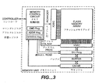
図3は、メモリアレイ並びに2つのレジスタ、すなわちキャッシュ(マスタデータレジスタ)およびバッファ(スレーブデータレジスタ)、を有するメモリユニットの例を示す。メモリアレイおよび接続されているレジスタは、両方のレジスタがバッファリング機能を提供するので、バッファ付きメモリアレイと見なされ得る。さらに、このメモリユニットは、コントローラと通信するメモリ制御回路を有する。コントローラとの通信は、チップイネーブル(CE)線、コマンドラッチイネーブル(CLE)線、アドレスラッチイネーブル(ALE)線、書き込みイネーブル(WE)線、読み出しイネーブル(RE)線、1組の入出力(I/O)線およびレディ/ビジー(R/B)線を含むことのある1群の線を介して行われる。このメモリユニットは、個々別々にまたは他のメモリユニットと共にパッケージ化され得る。一般に、図3に示されているもののようなメモリユニットは、1チップがメモリアレイおよびメモリ制御回路を含む1つのメモリユニットを有するように、専用メモリチップ上に形成される。コントローラからのホストデータは、メモリ制御回路によってキャッシュに、その後バッファに、その後フラッシュメモリアレイに送られ得る。これは、他のデータがバッファからフラッシュメモリアレイにプログラムされるのと同時にホストデータがキャッシュにロードされるのを可能にする。この並列性は、フラッシュメモリアレイへのデータ転送を高速化することができる。しかし、そのようなシステムからのレディ/ビジー信号は1ビットのデータを提供し得るに過ぎない。この信号は、アレイがアレイ・ビジーのような第1の状態にあるか、またはアレイ・レディのような第2の状態にあるかを表すことができる。しかし、キャッシュがビジーであるか否かのような付加的情報を知ることは有益である。 FIG. 3 shows an example of a memory unit having a memory array and two registers: a cache (master data register) and a buffer (slave data register). The memory array and the connected registers can be considered a buffered memory array because both registers provide a buffering function. The memory unit further includes a memory control circuit that communicates with the controller. Communication with the controller consists of a chip enable (CE) line, a command latch enable (CLE) line, an address latch enable (ALE) line, a write enable (WE) line, a read enable (RE) line, and a set of input / output (I / O) line and ready / busy (R / B) line. The memory units can be packaged individually or with other memory units. In general, a memory unit such as that shown in FIG. 3 is formed on a dedicated memory chip such that one chip has one memory unit including a memory array and a memory control circuit. Host data from the controller can be sent by the memory control circuit to the cache, then to the buffer, and then to the flash memory array. This allows host data to be loaded into the cache at the same time that other data is programmed from the buffer into the flash memory array. This parallelism can speed up data transfer to the flash memory array. However, a ready / busy signal from such a system can only provide one bit of data. This signal can indicate whether the array is in a first state, such as array busy, or in a second state, such as array ready. However, it is useful to know additional information such as whether the cache is busy.
従って、より多くの情報を単一の線に沿ってコントローラに提供することを可能にする制御システムに対するニーズがある。また、コントローラによって設定可能なシステムに対するニーズもある。他の集積回路とレディ/ビジー線を共有する個々の集積回路の状態をコントローラが判定することを可能にするシステムに対するニーズもある。
コントローラおよびメモリチップのような2つのコンポーネントを接続する単一の線を用いて付加的な機能を達成することを可能にするメモリ制御システムが開示される。メモリチップの何らかの状態をコントローラに示すためにレディ/ビジー線が使用される場合、メモリ制御システムは、同じ線を用いて付加的な情報を表すことを可能にすることができる。コントローラは、メモリチップにより送信される信号を設定するためにレジスタの内容をメモリチップに書き込むことができる。このようにして、コントローラは、レジスタを設定することによって、1つの範囲の可能な信号のうちからレディ/ビジー信号を選択することができる。選択された信号は、コントローラによる付加的な動作を必要とせずに、メモリチップからコントローラに提供される。コントローラは、メモリチップにおける状態を判定するためにメモリチップに積極的に問い合わせなくても良い。その代わりに、コントローラは、関心対象である状態を示す信号を受動的に受信することができる。或る設計では、コントローラは、エネルギーを節約する低電力或いは“スリープ”モードでそのような信号を受動的に受信することができる。コントローラは、信号が変化するときに給電状態に戻ることができる。例えば、コントローラは、メモリユニットがビジーである間は休眠し、メモリユニットが次のコマンドのためにレディになるときに目覚める。メモリアレイとキャッシュとを有するメモリユニットでは、メモリアレイの状態とキャッシュの状態とは別々の信号によって表示され得る。コントローラは、ビジー制御レジスタの内容を設定することによって、それらの信号のうちのどれをレディ/ビジー線でコントローラに送るかを選択することができる。 A memory control system is disclosed that allows additional functions to be achieved using a single line connecting two components, such as a controller and a memory chip. If a ready / busy line is used to indicate some state of the memory chip to the controller, the memory control system can allow the same line to be used to represent additional information. The controller can write the contents of the register to the memory chip to set the signal transmitted by the memory chip. In this way, the controller can select a ready / busy signal from a range of possible signals by setting a register. The selected signal is provided from the memory chip to the controller without requiring additional action by the controller. The controller may not actively query the memory chip to determine the state in the memory chip. Instead, the controller can passively receive a signal indicating the condition of interest. In some designs, the controller can passively receive such signals in a low power or “sleep” mode that conserves energy. The controller can return to the powered state when the signal changes. For example, the controller sleeps while the memory unit is busy and wakes up when the memory unit becomes ready for the next command. In a memory unit having a memory array and a cache, the state of the memory array and the state of the cache can be indicated by separate signals. The controller can select which of these signals to send to the controller on the ready / busy line by setting the contents of the busy control register.
コントローラは、特定のメモリチップからのビジー信号がマスクされて、レディ/ビジー線上の信号に影響を及ぼさないようにレジスタを設定することもできる。これは、複数のチップが同じレディ/ビジー線を共有する場合に有益である。マスクされていない1または複数のチップだけからコントローラが信号を受信するように個々のチップをマスクすることができる。このようにして、コントローラは、どのチップがそれ自体の信号をマスクしたのか、どれがそれ自体の信号をコントローラに送ったのかを明示的に識別することができる。 The controller can also set the register so that the busy signal from a particular memory chip is masked and does not affect the signal on the ready / busy line. This is beneficial when multiple chips share the same ready / busy line. Individual chips can be masked such that the controller receives signals from only one or more unmasked chips. In this way, the controller can explicitly identify which chip has masked its own signal and which has sent its own signal to the controller.
どのチップがそれ自体の信号をマスクすべきか、どれがそれ自体の信号を送るべきかをコントローラに個別に決定させる代わりとして、オートセレクトモードにおいてこの決定はチップのレベルで行われ得る。信号は、チップが選択されれば送信され、チップが選択されなければマスクされる。チップの選択は、この文脈では、チップを使用可能にする特定の線がアクティブであることを意味し、または、チップがコントローラコマンドによってまたはアクティブな使用可能化線とコマンドとの何らかの組み合わせによってアドレス指定されることを意味する。選択されるチップは、一般に、受信された最後のコマンドによりアドレス指定されたチップである。このシステムでは、選択されたチップだけがビジー信号を送る。1チップが選択解除されて他の一つが選択されるとき、選択解除されたチップ信号はマスクされ、選択されたチップ信号は、コントローラが別の設定変更を行うことを必要とせずに自動的にコントローラに送られる。これは、1つのチップに特有のレディ/ビジー信号を数個のチップにより共有されている線を介してコントローラが受信することを可能にする。信号は、どの信号が送信されてどれがマスクされるべきかをコントローラからの別のコマンドが指定することを必要とせずに、異なるチップが選択されるので、異なるチップから自動的に生じることができる。 Instead of having the controller individually determine which chip should mask its own signal and which should send its own signal, this determination can be made at the chip level in autoselect mode. The signal is transmitted if a chip is selected and masked if no chip is selected. Chip selection in this context means that a particular line that enables the chip is active, or the chip is addressed by a controller command or by some combination of an active enable line and command Means that The chip selected is generally the chip addressed by the last command received. In this system, only the selected chip sends a busy signal. When one chip is deselected and the other one is selected, the deselected chip signal is masked and the selected chip signal is automatically generated without requiring the controller to make another configuration change. Sent to the controller. This allows the controller to receive a ready / busy signal specific to one chip via a line shared by several chips. Signals can arise automatically from different chips because different chips are selected without requiring another command from the controller to specify which signals are sent and which should be masked. it can.
図4は、レディ/ビジー・ピン402を制御するために使用される信号制御システムについての等価回路400についての回路図を示す。マルチプレクサMUX1により受信される2つの信号、すなわちアレイ・ビジー信号406とキャッシュ・ビジー信号408と、が示されている。メモリ状態マシン410は、メモリのレディ/ビジー・ピン402を制御してどの信号がコントローラにより受信されるかを決定する出力412に信号406,408のどちらが加えられるかを決定する。一度に2つの信号、すなわちアレイ・ビジー406およびキャッシュ・ビジー408、のうちの1つだけが出力412に加えられる。状態マシン410は、出力412がメモリにより受信された最後のコマンドまたは他の何らかの要素に依存するように、動作することができる。出力412は、メモリ状態マシン410の現在の状態により決定されるので、メモリの状態を変更することなくコントローラにより直接設定することはできない。
FIG. 4 shows a circuit diagram for an
図5は、本発明の一実施形態に従う信号制御システムについての等価回路500についての回路図を示し、レディ/ビジー信号がメモリユニットにおけるちょうど2つよりも多くの状態を表すことができるようにレディ/ビジー線を介して付加的なデータを送ることを可能にする。この制御システムは、図示された制御回路としてまたは何らかの同等の仕方で実現され得る。第1のマルチプレクサMUX1が設けられ、アレイとキャッシュの状態を各々示す入力アレイ・ビジー406とキャッシュ・ビジー408とを有する。MUX1の出力は、メモリ状態マシン410の状態に応じて前述したように選択される。従って、MUX1の出力は、前述した出力412と同等である。しかし、前の回路とは違って、図5は、MUX1の出力が第2のマルチプレクサMUX2へ進むことを示し、ビジー制御レジスタ522によって制御される。MUX2の出力524は制御システムのビジー出力になる。従って、MUX2は、前述した出力412と、このシステムによって提供される出力との間に挿入されている。これにより、ビジー制御レジスタ522の内容の改変を通して出力524を設定することを可能にする。ビジー制御レジスタ522の内容は、コントローラによって直接に改変され得る。
FIG. 5 shows a circuit diagram for an
ビジー出力524は、MUX2への入力から選択され得る。MUX2への入力は、MUX1の出力412と、アレイ・ビジー406と、キャッシュ・ビジー408と他のビジー・ソース526とを含む。図5は、他のビジー・ソース526を表す単一の線を示している。しかし、他のビジー・ソース526は、メモリユニット内の複数の状態を表すMUX2への複数の入力を含み得る。従って、出力524の意味は、所望されている情報に応じて設定され得る。
MUX2の1つの可能な出力は単にMUX1の出力である。この場合、制御回路は、あたかもMUX2が存在しないかのように動作する。従って、制御システムは、逆互換性が維持され得るように、図4の前述した制御システムとして動作するように構成され得る。 One possible output of MUX2 is simply the output of MUX1. In this case, the control circuit operates as if MUX2 does not exist. Accordingly, the control system can be configured to operate as the previously described control system of FIG. 4 such that reverse compatibility can be maintained.
MUX2の出力としてアレイ・ビジー406またはキャッシュ・ビジー408が選択され得る。これらもMUX1の可能な出力であるが、MUX1の出力はコントローラが改変することのできるレジスタの内容に応じて設定可能ではない。MUX1により生成される信号はメモリ状態マシン410の現在の状態に基づいて確定的に作られるが、MUX2により生成される信号はコントローラが改変しうる設定可能な仕方で作られる。このシステムでは、出力はコントローラによって直接選択され得る。その選択は、メモリユニットがコマンドを実行して動作している間に変更され得る。
Array busy 406 or cache busy 408 may be selected as the output of MUX2. These are also possible outputs of MUX1, but the output of MUX1 is not settable depending on the contents of the registers that can be modified by the controller. The signal generated by MUX1 is deterministically generated based on the current state of
MUX2の出力は、ドレイン530がレディ/ビジー・ピン502に接続され、ソースが接地に接続されているトランジスタ528のゲートに進む。動作時に、レディ/ビジー・ピン502は、コントローラに接続する信号線に接続され得る。MUX2の出力が“ハイ”でビジー状態を表しているとき、トランジスタ528はオンに転換され、レディ/ビジー・ピン502の電圧は接地すなわち“ロー”にされる。MUX2の出力が“ロー”でレディ状態を表しているとき、トランジスタ528はオフに転換されてレディ/ビジー・ピン502の電圧は“ハイ”レベル、すなわち信号線に接続されている供給の電圧に上昇する。従って、トランジスタ528は、MUX2からの出力524のインバータとして働く。
The output of MUX2 goes to the gate of
前の記述は制御回路にマルチプレクサを用いる特定の例に言及しているが、前述したような手法は特定のハードウェア構成に限定されない。前述した例は、いろいろなハードウェアを用いて実行され得るか、或いはソフトウェアを用いて達成され得る技術を説明している。図示されている制御回路は、使用され得る種々の制御システムのための等価回路と見なされて良い。制御システムは、種々の制御回路を用いて或いはソフトウェアを用いて種々に実現され得る。 Although the previous description refers to the specific example of using a multiplexer in the control circuit, the approach as described above is not limited to a specific hardware configuration. The examples described above describe techniques that can be implemented using a variety of hardware or that can be accomplished using software. The illustrated control circuit may be considered as an equivalent circuit for various control systems that may be used. The control system can be implemented in various ways using various control circuits or using software.
或る例では、2つ以上の制御システムが1つの共通信号線に接続される。従って、図5のレディ/ビジー・ピンは、共有される信号線によって他の制御システムの他のレディ/ビジー・ピンに接続され得る。そのような線は、導電性材料の1つ以上の連続する部分から作られ得る。例えば、プリント回路基板上に形成された金属トレースは信号線または信号線の一部を形成することができる。しかし、そのような共有される線は特定の集積回路の状態を隠すことがある。たった1つの集積回路がビジーであるに過ぎないときでも、その制御システムは、対応するレディ/ビジー・ピンを“ロー”状態にするハイ出力を生じさせる。これは、接続されている信号線をローにする。その制御システムが信号線に接続されている他の全ての集積回路の状態はコントローラには分からないように隠される。これは、これらの制御システムの出力における如何なる変化もコントローラによって検出されないということを意味する。他の制御回路出力がレディからビジーに遷移しているならば、これはコントローラによっては検出され得ない。なぜならば、それは既にビジー信号を受信しているからである。従って、ホストにより受信されるビジー信号は、集積回路がビジーであることを示すだけであって、どれがそうなのかは示さない。 In one example, two or more control systems are connected to one common signal line. Thus, the ready / busy pins of FIG. 5 can be connected to other ready / busy pins of other control systems by shared signal lines. Such a line can be made from one or more consecutive portions of conductive material. For example, a metal trace formed on a printed circuit board can form a signal line or part of a signal line. However, such shared lines may hide certain integrated circuit states. Even when only one integrated circuit is busy, the control system produces a high output that places the corresponding ready / busy pin in a “low” state. This causes the connected signal line to go low. The state of all other integrated circuits whose control system is connected to the signal lines is hidden from the controller. This means that no change in the output of these control systems is detected by the controller. If other control circuit outputs are transitioning from ready to busy, this cannot be detected by the controller. This is because it has already received a busy signal. Thus, the busy signal received by the host only indicates that the integrated circuit is busy and does not indicate which is.
本発明の一実施形態では、コントローラに必要とされる制御システム出力をマスクするためにビジー制御レジスタを使用することができる。従って、入力406,408によってどのような状態が制御システムに対して示されていても、出力524はビジー制御レジスタ522の1つ以上のビットに応じてローに保たれ得る。このディスエーブル機能は、コントローラが監視されるべき1つ以上の集積回路を識別し、他の集積回路を無視することを可能にする。
In one embodiment of the present invention, a busy control register can be used to mask the control system output required for the controller. Thus, whatever state is indicated to the control system by
本発明の他の実施形態では、ビジー制御レジスタによってオートセレクト機能が使用可能にされ得る。この機能は、制御システムに接続されている集積回路が選択されているか否かによって選択的に制御システムがその出力をマスクすることを可能にする。オートセレクト機能は、対応する集積回路が選択されていなければMUX2の出力524を使用禁止にする。これは、直接的コントローラ介入無しでオートセレクトモードで制御システムのレベルで自動的に行われる。従って、コントローラによってオートセレクトが使用可能にされると、制御システムはコントローラから制御システムへのさらなる入力無しでその信号を適宜送信するかまたはマスクすることができる。選択は、チップイネーブル(CE)線の状態によりまたは最後にアドレス指定された集積回路若しくはこれら2つの要素の何らかの組み合わせによって決定され得る。オートセレクトを目的としてどの基準が選択を決定するかを選択するためにビジー制御レジスタ522の付加的なビットが使用され得る。例えば、CE信号に基づく選択、最後にアドレス指定されたコマンドに基づく選択およびこれらの基準の両方に基づく選択は、3つの異なるオートセレクト可能性を提供する。オートセレクトを使用禁止にする可能性もあり、合計4個の可能性を提供する。これら4つの可能性は、例えばビット5および7などの、ビジー制御レジスタ522の2つのビットを用いて選択され得る。
In other embodiments of the present invention, the autoselect function may be enabled by a busy control register. This function allows the control system to selectively mask its output depending on whether an integrated circuit connected to the control system is selected. The autoselect function disables the
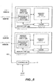
記載された制御システムを用いるメモリユニットを有するメモリシステムの例が図6に示されている。2つのメモリユニット640,642が示されている。メモリユニット640は、レディ/ビジー制御回路646を含むメモリ制御回路644を有する。メモリユニット642はレディ/ビジー・ピン650を含むメモリ制御回路648を有する。両方のレディ/ビジー制御回路646,650が共通信号線に接続されている。共通信号線は、他のメモリユニットにも延びることができる。オートセレクトがレディ/ビジー回路で使用可能にされている場合、その回路からのレディ/ビジー信号は、そのレディ/ビジー回路を含むメモリユニットが選択されなければマスクされる(レディ状態に保たれる)。一般に、オートセレクトは、1つのコントローラに一緒に接続されている全てのメモリユニットについて使用可能または使用禁止にされる。このようにして、コントローラによって選択されたメモリユニットのレディ/ビジー信号だけがコントローラに送られる。使用可能にされていないメモリユニットのレディ/ビジー信号はレディ/ビジー制御回路によってマスクされる。この構成では、レディ/ビジー信号はメモリユニットがビジーであることだけを示すのではなくて、どの特定のメモリユニットがビジーであるのかも示す。なぜならば、一般に、一度に唯一のメモリユニットが選択されるからである。2つ以上のメモリユニットが選択され、オートセレクトが使用可能にされるならば、ビジー信号は、選択されたメモリユニットのうちのいずれからも生じ得る。例えば、図6のメモリユニット(メモリユニット640,642および信号線に接続されている任意の付加的メモリユニット)についてオートセレクトが使用可能にされている場合、メモリユニット640が選択されれば、メモリユニット640からのレディ/ビジー信号だけがコントローラにより受信される。この状態で、メモリユニット642のメモリアレイまたはキャッシュは何らかの最近のコマンドから依然としてビジーであり得る。しかし、メモリユニット642は選択されず、メモリ640が選択される。メモリユニット642にビジー状態が存在し得るが、この状態を示す信号はコントローラに送られない。代りに、信号はメモリユニット642のレディ/ビジー制御回路650によってマスクされる。同様に、信号線652に接続されている他のメモリユニットからのビジー信号は、メモリユニットが選択されていなければ、そのレディ/ビジー制御回路によってマスクされる。
An example of a memory system having a memory unit using the described control system is shown in FIG. Two
図7は代替の実施形態を示し、この場合、どのメモリユニットとも別のレディ/ビジー制御回路760に数個のメモリユニットが接続されている。各メモリユニット762,764は単数または複数のレディ/ビジー出力を有する(1本の線だけが示されているが、アレイ・ビジー、キャッシュ・ビジーおよび他のビジー信号のために個別の線を設けることができる)。レディ/ビジー制御回路760は前述したのと同様に動作するが、別のダイ上に位置する。レディ/ビジー制御回路760は、専用のダイ上に、または他の回路と共に1つのインターフェイスの一部として、実現され得る。この構成は、複数のメモリダイが単一のパッケージにパッケージ化される場合に使用され得る。パッケージのために唯一のレディ/ビジー・ピンが必要とされるように、複数のレディ/ビジー制御回路を有する1つのダイをパッケージに含ませることができる。通常、コントローラは別のダイ上にある。
FIG. 7 shows an alternative embodiment in which several memory units are connected to a ready / busy control circuit 760 that is separate from any memory unit. Each
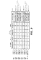
図8は、ビジー制御レジスタ522を示す。ビジー制御レジスタは、8個のデータビットを有するものとして示されている。しかし、この例では、ビット2〜5は使用されず、付加的な機能のために確保される。ビット0〜1は、ビジー制御回路への4つの入力のうちのどれがコントローラに提供されるかを示す。これらの入力は、アレイ・ビジー、キャッシュ・ビジー、内部ビジー(MUX1の出力)および他のビジーを含む。“他のビジー”は1本の線として示されているが、付加的なビジー信号および付加的な線があっても良い。この理由から、より多くの入力から選択を行えるようにビット2〜5が確保される。ビット6はディスエーブルビットである。ビット6が1にセットされているときには、ビジー制御回路の出力はビジー制御回路への入力に関わらずに“レディ”状態にとどまる。ビット7はオートセレクトビットである。ビット7が1にセットされているときには、ビジー制御回路の出力は、そのメモリユニットがコントローラによって選択されているか否かによる。コントローラは、そのチップに対応するチップイネーブル(CE)信号をオンに転換させることによってメモリユニットを選択することができる。しかし、複数のメモリユニットが一緒にパッケージ化される場合、それらは1つのCE線を共有することができる。従って、CE線による如何なる選択も個々のメモリユニットを充分に特定することはできない。メモリユニットは、コントローラによってコマンドで提供されるアドレスによって特定され得る。コントローラがコマンドを送るとき、個々のメモリユニットに特有のアドレスを含むことができる。受信された最後のコマンドで提供されるアドレスが、選択されたメモリユニットのアドレスであると見なされ得る。従って、コントローラがメモリユニットを選択する2つの手法が記載される。メモリシステムは、メモリユニットを特定するためにこれらの手法のいずれかまたはその2つの組み合わせを用いることができる。例えば、メモリユニットは、CE線が選択され、かつ最後のコマンドがメモリユニットのアドレスを特定したならば、選択され得る。ビジー制御レジスタのいろいろなビットの重要性は、いろいろな実施形態において一様でない。例えば、ビット2〜5は図8のビジー制御レジスタにおいては削除されても良い。或る実施形態では、オートセレクトは、この機能を使用可能/使用禁止にするビットが必要でないように、永久的に使用可能にされてもよい。
FIG. 8 shows the
図9は、図8に示されているビジー制御レジスタ522の内容についての真理値表を示す。ビジー制御回路の出力524は,”ビジー”の下の右側列にある。線1はディスエーブル=1を示す。この状態では、ビジー制御レジスタの他の内容に関わらず、出力は0或いはローにとどまる。このロー出力は、出力がレディ/ビジー線に接続されているオープンドレイントランジスタ528のゲートに達するので、レディ/ビジー・ピン502および接続されているレディ/ビジー線の電圧がハイ(レディ)にとどまることを意味する。線2〜5は“選択”ビットのいろいろな値についての出力を示す。4つの出力は、図5のMUX1の出力である内部ビジー412を含む。キャッシュ・ビジー408およびアレイ・ビジー406は、キャッシュおよびアレイの状態を各々表し、別々に選択され得る。他のビジー526は、コントローラによって使用され得る任意のビジー信号であって良い。さらに、ビット2〜5は、必要ならば付加的なビジー信号を選択するために、使用され得る。これらは図9の真理値表には示されていない。線6は、オートセレクト=1(オートセレクトが使用可能にされている)およびダイ選択=0(ダイが選択されていない)を示す。この状態における出力0である。なぜならば、オートセレクトが使用可能にされているときには、コントローラがダイを選択しなければ出力がマスクされるからである。ここではダイは選択されていないので出力はマスクされたままである、すなわち、0にとどまり、従ってレディ/ビジー線は影響を受けない。線7〜10は、オートセレクト=1(オートセレクトが使用可能にされている)およびダイ選択=1(ダイが選択されている)のときの出力を示す。この場合の出力は選択ビットによる。この場合には選択されたどのような信号も出力として供給される。なぜならば、出力がマスクされないからである。ビジー制御レジスタ522がメモリユニットのレディ/ビジー出力を設定する柔軟な方法を提供することが分かる。ビジー制御レジスタ522の内容は、レディ/ビジー信号の意味が所望の意味に設定されるように、改変され得る。ビジー信号はマスクされ得る。単一のコントローラに複数のメモリユニットが接続されている場合には、マスキングはコントローラが単一のメモリユニットを監視することを可能にすることができる。なぜならば、他の信号がマスクされるからである。これらのいろいろなオプションは、ビジー制御レジスタの内容を改変することによってコントローラにより選択され得る。
FIG. 9 shows a truth table for the contents of the busy control register 522 shown in FIG. The
ビジー制御レジスタ522の内容は、メモリユニットのアドレスと書き込まれるべき内容とを指定するコマンドを用いてコントローラによって直接書き込まれ得る。図10は、メモリユニットとコントローラとを接続する複数の線を有するメモリユニットにより受信されるそのようなコマンドについてのタイミング図を示す。チップイネーブル(CE)線上の信号は、メモリユニットの動作を可能にするために下げられる。コマンドラッチイネーブル線(CLE)は、コマンドをI/Oポートからコマンドレジスタにラッチすることを可能にするために高められる。CLE線がハイであるとき、コマンド(C)がコマンドレジスタに転送され得るようにI/O線0〜7からのデータの取得を可能にするために書き込みイネーブル(WE)が下げられる。コマンド(C)は、ビジー制御書き込みのためのコマンドコードを表し、ビジー制御レジスタの内容が書き込まれることを示す。コマンドの最後にWE線が高められる。次に、アドレス情報をアドレスレジスタにラッチすることを可能にするためにアドレスラッチイネーブル(ALE)信号が高められる。再び、I/O線0〜7でのアドレスデータの転送を可能にするためにWE信号が下げられる。アドレスデータは特定のメモリユニットのアドレス(A)を含む。この場合、アドレス指定されるメモリユニットは、コントローラが更新するビジー制御レジスタを有するメモリユニットである。選択されたレジスタの内容(S)がI/O線0〜7からアドレス指定されたメモリユニットのビジー制御レジスタに転送されることを可能にするためにWE信号が3度目に下げられる。選択されたレジスタの内容Sは、メモリユニットからのレディ/ビジー信号を設定するためにビジー制御レジスタ522にロードされるべきデータビットを含む。メモリユニットのレディ/ビジー出力は、レディ/ビジー制御レジスタ522の内容が改変されるときのレディ/ビジー信号の遷移も表すように示されている。この様な結果が生じるのは、信号が第1の状態(例えば、アレイ・ビジー)の表示から第2の状態(例えば、キャッシュ・レディ)へ変化するからである。レディ/ビジー信号におけるこの変化は、単に、メモリユニットの状態が変化したことではなくて信号の意味が変化したことを反映しているに過ぎない。 The contents of the busy control register 522 can be written directly by the controller using commands that specify the address of the memory unit and the contents to be written. FIG. 10 shows a timing diagram for such a command received by a memory unit having a plurality of lines connecting the memory unit and the controller. The signal on the chip enable (CE) line is lowered to allow operation of the memory unit. The command latch enable line (CLE) is raised to allow commands to be latched from the I / O port into the command register. When the CLE line is high, the write enable (WE) is lowered to allow acquisition of data from the I / O lines 0-7 so that the command (C) can be transferred to the command register. Command (C) represents a command code for busy control writing, and indicates that the contents of the busy control register are written. The WE line is raised at the end of the command. Next, the address latch enable (ALE) signal is raised to allow the address information to be latched into the address register. Again, the WE signal is lowered to enable address data transfer on I / O lines 0-7. The address data includes an address (A) of a specific memory unit. In this case, the addressed memory unit is a memory unit having a busy control register that is updated by the controller. The WE signal is lowered a third time to allow the contents (S) of the selected register to be transferred from I / O lines 0-7 to the busy control register of the addressed memory unit. The selected register content S includes data bits to be loaded into the busy control register 522 to set the ready / busy signal from the memory unit. The ready / busy output of the memory unit is shown to also represent the transition of the ready / busy signal when the contents of the ready / busy control register 522 are modified. Such a result occurs because the signal changes from an indication of a first state (eg, array busy) to a second state (eg, cache ready). This change in the ready / busy signal simply reflects a change in the meaning of the signal, not a change in the state of the memory unit.
或る例では、1つのコントローラに接続されている全てのメモリユニットのレディ/ビジー制御レジスタの内容を変更することが望ましい。そのような場合には、ビジー制御書き込みコマンドを特定のユニットに対してアドレス指定する必要はない。図11は、メモリユニットアドレスを指定しないビジー制御書き込みコマンドの例を示す。タイミング図は図10に示されているものに類似するが、コントローラによって送られるアドレスは無い。そのようなアドレス指定されていないコマンドは、コントローラに個々のメモリユニットだけが接続されている場合またはCE線が個々のメモリユニットを特定するのに充分である場合に(例えば、CE線が共有されていない)送信され得る。アドレス指定されていないコマンドは、複数のメモリユニットが1つのコントローラに接続されていてメモリユニットの全てのビジー制御レジスタの内容を同時に同じ内容を有するように設定することが望ましい場合にも使用され得る。そのようなコマンドは、全てのメモリユニットが同じレジスタ内容を受け取るように、オンのCEを有する全ての接続されているメモリユニットに同時に一斉送信される。例えば、前述したオートセレクト機能は、通常、全てのメモリユニットについて同時に使用可能にされる。そのような一斉送信されるコマンドは、各ビジー制御レジスタの内容を別々のコマンドで別々に書き込む動作と比べて時間を節約することができる。 In one example, it may be desirable to change the contents of the ready / busy control registers of all memory units connected to one controller. In such cases, the busy control write command need not be addressed to a particular unit. FIG. 11 shows an example of a busy control write command that does not specify a memory unit address. The timing diagram is similar to that shown in FIG. 10, but no address is sent by the controller. Such an unaddressed command is used when only individual memory units are connected to the controller or when the CE line is sufficient to identify an individual memory unit (eg, the CE line is shared). Not be sent). Non-addressed commands can also be used when multiple memory units are connected to one controller and it is desirable to set the contents of all busy control registers of the memory units to have the same contents at the same time . Such a command is broadcast simultaneously to all connected memory units with CEs on so that all memory units receive the same register contents. For example, the above-described autoselect function is normally enabled for all memory units simultaneously. Such broadcast commands can save time compared to the operation of writing the contents of each busy control register separately with separate commands.
ビジー制御レジスタの内容を書き換えるコマンドは、メモリユニットがコマンドを受信できるときには何時でも送信され得る。或る実施形態では、レディ/ビジー信号はメモリユニットが1つの動作を実行している間にアレイ・ビジーからキャッシュ・ビジーへ転換され得る。メモリの設計によっては、データがメモリアレイにプログラムされている間にビジー制御レジスタを設定することが可能である。 A command to rewrite the contents of the busy control register can be sent whenever the memory unit can receive the command. In some embodiments, the ready / busy signal may be switched from array busy to cache busy while the memory unit is performing one operation. Depending on the memory design, the busy control register can be set while data is programmed into the memory array.
図12A〜12Gは、図3に示されているもののようなキャッシュを有するバッファ付き不揮発性メモリアレイで本発明のいくつかの態様が使用される仕方の例を示す。図12は、キャッシュを有するバッファ付きメモリアレイにおけるデータ格納動作の連続するステップを示す。 12A-12G illustrate examples of how some aspects of the invention may be used in a buffered non-volatile memory array having a cache such as that shown in FIG. FIG. 12 shows the successive steps of the data storage operation in a buffered memory array with a cache.
図12Aは、メモリアレイ1270、バッファ1272、キャッシュ1274およびコントローラ1276を示している。この図では、メモリアレイの隣の“R”およびキャッシュ1274の隣の“R”によって示されているようにキャッシュ1247およびメモリアレイ1270の両方がレディである。バッファ1272およびキャッシュ1274は2つのレジスタであり、各レジスタがメモリアレイにプログラムされるべきデータのページを保持する。
FIG. 12A shows
図12Bではデータがコントローラ1276からキャッシュ1274に転送される。これは、メモリアレイ内のデータが格納されるべき場所を指定する書き込みコマンドのようなコントローラからのコマンドに応答して行われ得る。通常、コントローラから受信された最後のコマンドにレディ/ビジー信号が結合されるシステムでは、この状態において書き込みコマンドはキャッシュ・ビジー信号をコントローラに供給させる。これはキャッシュが利用可能になったならば直ちにコントローラが他のデータもキャッシュに送れるようにするためである。図12Bは、データがコントローラ1276からキャッシュ1274に転送されることを示している。そのような操作に必要とされる時間は、キャッシュ1274に格納されるデータの量による。それは一般に1ページのデータである。単一のセクタのデータを保持するページのためには、約10マイクロ秒が必要とされ得る。メタブロックを用いる設計の場合のように、メモリユニットが複数のセクタを並列にプログラムする場合、キャッシュ1274はおそらく1セクタよりはるかに大きくなり得る。例えば、1つのメタブロックが16個のブロックを含む場合、1つのメタページは16セクタのデータを含み得る。従って、キャッシュ1274も16セクタのデータを保持する。16セクタのデータを転送するために必要な時間は約160マイクロ秒である。この動作中、キャッシュ1274の隣の“R”によって示されているようにキャッシュ1274はレディであって、コントローラ1276がデータを送り続けることを可能にする。文字“R”および“B”は、図12の全体において、隣の部品の状態をレディ(R)またはビジー“B”として示す。メモリアレイ1270はこのときレディ状態にとどまっている。なぜならば、データがアレイに書き込まれないからである。キャッシュ1274へのデータ転送が完了したとき、キャッシュ1274はビジー状態である。なぜならば、それはデータを含んでいて、コントローラ1276からそれ以上のデータを受け入れることができないからである。
In FIG. 12B, data is transferred from the
図12Cは、キャッシュ1276からバッファ1272へのデータの転送を示す。これは割合に迅速な動作であって、3マイクロ秒未満で行われ得る。このステップの間、キャッシュ1274はビジーのままであり、メモリアレイ1270はレディのままである。
FIG. 12C shows the transfer of data from the
図12Dは、バッファ1272に転送されたデータがメモリアレイ1270に引き渡されることを示す。このステップでは、メモリアレイ1270は、書き込まれるので、ビジーである。しかし、キャッシュ1274は、キャッシュ1274内にあったデータがバッファ1272への転送を完了したならば、レディになる。このレディ状態は、もっと多くのデータもキャッシュ1274に送れるように、コントローラ1276に信号され得る。この時点では、データの転送をなるべく早く開始できるように、キャッシュ・レディ/ビジー信号はコントローラにとって重要である。
FIG. 12D shows that the data transferred to the
図12Eは、前のステップから直ちに続き、メモリアレイ1270へのデータのプログラミングと並行してデータがキャッシュ1274に送られることを示す。この同時動作は、コントローラ1276からメモリアレイ1270へのより高速のデータ転送を可能にすることができる。メモリアレイ1270へのデータのプログラミングは、約150マイクロ秒から1000マイクロ秒を必要とする割合に低速の動作であるので、この時間中に他の動作を実行することは全体としての動作速度にとっておそらく重要である。このステップ中は、メモリアレイはビジーであるがキャッシュ1274はレディである。プログラミングのために高度の並行性が用いられる場合(例えば、メタブロックが使用される場合)、メモリアレイ1270へのプログラミングはキャッシュ1274へのデータの転送より高速であり得る。しかし、一般にキャッシュ1274への転送が先に完了する。
FIG. 12E continues immediately from the previous step and shows that data is sent to the
図12Fは、キャッシュ1274を満たすように全てのデータがコントローラ1276から転送された後の状態を示す。キャッシュ1274はデータを含み、従ってビジー状態にある。メモリアレイ1270へのデータのプログラミングは、この図では続行中であるとして示されている。この例では、メモリアレイ1270へのプログラミングは、キャッシュ1274へのデータ転送が終了した後も続行される。しかし、他の例では、これら2つの動作は同時に終了するかも知れず、或いはメモリアレイ1270のプログラミングが先に終了するかもしれない。
FIG. 12F shows the state after all data has been transferred from the
図12Gは、メモリアレイ1270およびキャッシュ1274へのデータの書き込みの完了後の状態を示す。この段階でメモリアレイ1270はレディである。なぜならば、それは最早データをプログラムするビジーではないからである。キャッシュ1274はビジーである。なぜならば、そこにデータが既に格納されているのでコントローラ1276から新しいデータを受け入れることができないからである。
FIG. 12G shows a state after data writing to the
図12Hは、図12Cの場合と同様にキャッシュ1274からバッファ1272へのデータの転送を示す。この段階では、追加のデータがコントローラ1276により供給され得るので、サイクルは図12Dに示されているステップに戻る。コントローラがデータを供給している間は、図12D〜12Gに示されているステップが複数回反復され得る。
FIG. 12H illustrates the transfer of data from the
図12Iは、図12Hにおけるキャッシュ1274からバッファ1272へのデータの転送の完了後の状態を示す。ここでは、書き込み動作が進行中なので、メモリアレイ1270はビジーである。キャッシュ1274は、他のデータを受け入れることができるので、レディである。しかし、この場合にはコントローラ1276はメモリアレイ1270に格納されるべきデータをそれ以上持っていない。従って、キャッシュ1274はレディ状態にとどまり続け、メモリアレイ1270はデータが書き込まれている間はビジー状態にとどまる。
FIG. 12I shows a state after the transfer of data from the
通常、レディ/ビジー線を介してコントローラ1270に送られる信号は、メモリアレイの状態またはキャッシュの状態のいずれかを示す。図12A〜12Hに関して記載されたような書き込みシーケンスの間、レディ/ビジー線は一般にキャッシュ1274がそれ以上のデータを受け入れる準備ができていることを示す信号を送る。この信号は、レディ信号がコントローラにより受信されたならば直ちにそれ以上のデータを送信し得るように、選択される。書き込みシーケンス中、コントローラにとってはキャッシュ1274の状態に関する情報は一般にメモリアレイ1270の状態に関する情報よりも重要である。しかし、図12Hに示されている段階では、キャッシュ1274の状態ではなくてメモリアレイ1270の状態を知ることの方が望ましい。なぜならば、キャッシュ1274に送るべきデータがそれ以上は無く、従ってキャッシュ1274の状態は必要とされないからである。メモリアレイ1270がレディになるまで、コントローラ1276は書き込み動作のような他の動作を開始することはできない。なぜならば、メモリアレイがレディになるまでは、プログラムされていないデータが依然としてバッファ1272内にあるからである。
Typically, the signal sent to the
或るメモリシステムでは状態レジスタが設けられ、それはメモリシステムの部分の状態を示す。図12Iは状態レジスタ1278を示し、これは、メモリアレイ1270がレディであるのかビジーであるのかを示し、またキャッシュ1274がレディであるのかビジーであるのかを示す。状態レジスタは通常メモリユニットの部分である。それは、コントローラが能動的に内容を読む場合、コントローラによってポーリングされ得る。しかし、メモリユニットにおける状態をコントローラに知らせるこの方法は理想的ではない。ポーリングはかなりの電力を必要とし得る。また、低消費電力モードを有するコントローラでは、ポーリング動作を実行するためにコントローラを充分に給電される状態に保つことが必要であり得る。図12Iに示されている状態では、コントローラ1276は、メモリアレイ1270がビジー状態からレディ状態に変化するまで、状態レジスタ1278に繰り返しポーリングする必要がある。
Some memory systems are provided with a status register, which indicates the status of a portion of the memory system. FIG. 12I shows the status register 1278, which indicates whether the
本発明の1つの実施形態では、コントローラ1270はメモリユニットからレディ/ビジー線でどの信号が送られるかを選択することができる。図12A〜Iに示されている状態では、これはおそらく一定の利点を有することができる。図12A〜12Eに示されているプロセスステップについて、キャッシュ1274がどの状態であるのかを示す信号をコントローラ1276が受信するのが有利であり得る。これはコントローラがデータをメモリユニットに迅速に送ることを可能にする。なぜならば、キャッシュ1274がレディになったならば直ちに追加のデータが送られるからである。しかし、メモリユニットに送られるべき追加のデータをコントローラ1276が持っていない図12Iに示されている状態では、コントローラ1276はキャッシュ1274の状態を知る必要はない。この段階で、メモリアレイ1270の状態が、レディ/ビジー線で送られる出力として選択され得る。この選択は、ビジー制御レジスタ522の内容を変更することによってコントローラ1276により行われ得る。
In one embodiment of the invention, the
或る設計では、コントローラは、コントローラによる電力消費が低減される低消費電力または“スリープ”モードを有することができる。コントローラがそのような低消費電力モードで費やす時間が長いほど少ない電力が消費される。従って、動作と動作の間、或いは直接的なコントローラ関与を必要としない何らかの動作がメモリユニットにより実行されている間を含む可能な時に、コントローラを低電力消費モードにすることができる。或る例では、レディ/ビジー信号のような信号線の変化に応じてコントローラを全出力モードに戻すことができる。すなわち、コントローラが次の動作を実行する時間になった時にコントローラを“目覚めさせる”ことができる。例えば、図12Iにおいて、アレイ・ビジー信号がレディ/ビジー線でコントローラに送られるようにビジー制御レジスタの内容を変化させるコマンドをコントローラは送ることができる。すると、コントローラは、レディ/ビジー線でレディ信号が受信されるまでスリープモードに入ることができる。これは、状態レジスタに繰り返しポーリングすることと比べて大幅に電力を節約することができ、またコントローラにおいて実行しやすい。そのような電力節約は、バッテリー電力に依存し、従って限られた電力供給を有するデジタルカメラおよびMP3プレーヤーのような携帯可能の装置で使用されるメモリシステムのためには特に重要である。 In some designs, the controller may have a low power consumption or “sleep” mode in which power consumption by the controller is reduced. The longer the controller spends in such a low power consumption mode, the less power is consumed. Thus, the controller can be put into a low power consumption mode when possible, including between operations, or while some operation that does not require direct controller involvement is being performed by the memory unit. In one example, the controller can be returned to full output mode in response to signal line changes such as ready / busy signals. That is, it is possible to “wake up” the controller when it is time for the controller to perform the next operation. For example, in FIG. 12I, the controller can send a command to change the contents of the busy control register so that an array busy signal is sent to the controller on the ready / busy line. The controller can then enter sleep mode until a ready signal is received on the ready / busy line. This can save significant power compared to repeatedly polling the status register and is easy to implement in the controller. Such power savings are especially important for memory systems that are dependent on battery power and are therefore used in portable devices such as digital cameras and MP3 players with limited power supply.
前述した例は、取り外し可能なメモリカードに見られるようなキャッシュを有するバッファ付き不揮発性メモリに関連する。しかし、本発明のいろいろな態様は他の用途において他の集積回路にも適用され得る。揮発性メモリ製品を含む他の記憶装置は、同様の手法を用いて単一の線からより大きな機能性を達成することができる。ノンメモリの用途も、前述したような手法を用いることができる。 The foregoing example relates to a buffered non-volatile memory having a cache such as found on a removable memory card. However, various aspects of the invention may be applied to other integrated circuits in other applications. Other storage devices, including volatile memory products, can achieve greater functionality from a single line using similar techniques. For non-memory applications, the method described above can be used.
前の説明は特定の実施形態についての充分な記述であるが、種々の改変、代替の構成および同等物を使用することができる。従って、前述した記述および図解は、請求項によって定義される本発明の範囲を限定するものと介されるべきではない。 While the preceding description is a complete description of specific embodiments, various modifications, alternative configurations and equivalents may be used. Therefore, the above description and illustrations should not be taken as limiting the scope of the invention which is defined by the claims.
Claims (18)
不揮発性メモリセルのバッファ付きアレイと、
前記メモリユニットからの出力信号を制御レジスタ内のデータビットに従って複数の信号から選択する制御回路であって、前記複数の信号は、前記バッファ付きメモリアレイが第1の状態にあるのかそれとも第2の状態にあるのかを示す第1の信号と、前記バッファ付きメモリアレイが第3の状態にあるのかそれとも第4の状態にあるのかを示す第2の信号とを含む制御回路と、
を備えるメモリユニット。 A memory unit that communicates with a memory controller via a signal line in a memory system,
A buffered array of non-volatile memory cells; and
A control circuit for selecting an output signal from the memory unit from a plurality of signals according to data bits in a control register, wherein the plurality of signals are based on whether the buffered memory array is in a first state or a second state; A control circuit comprising: a first signal indicating whether the buffered memory array is in a third state; or a second signal indicating whether the buffered memory array is in a third state or a fourth state;
A memory unit comprising:
コントローラと、
不揮発性メモリセルのアレイと、
前記不揮発性メモリセルのアレイにプログラムされるべきデータを保持するように前記不揮発性メモリセルのアレイに接続されたキャッシュと、
前記不揮発性メモリセルのアレイのレディ/ビジー状態を示す第1の信号と前記キャッシュのレディ/ビジー状態を示す第2の信号とを含む複数の信号から前記コントローラへの出力信号を選択する制御レジスタと、
を備えるメモリシステム。 A memory system having a buffered non-volatile memory array in communication with a controller comprising:
A controller,
An array of non-volatile memory cells;
A cache connected to the array of non-volatile memory cells to hold data to be programmed into the array of non-volatile memory cells;
A control register for selecting an output signal to the controller from a plurality of signals including a first signal indicating a ready / busy state of the array of nonvolatile memory cells and a second signal indicating a ready / busy state of the cache When,
A memory system comprising:
前記複数の集積回路のためにオートセレクトモードが使用可能にされているとき、前記コントローラによる前記集積回路の選択に応答して前記集積回路から前記コントローラに前記レディ/ビジー信号を送るステップと、
前記複数の集積回路のために前記オートセレクトモードが使用可能にされているとき、前記集積回路が前記コントローラによって選択されたときには前記複数の集積回路のうちの他のものからのレディ/ビジー信号が前記コントローラに送られないように前記複数の集積回路のうちの他のものからの前記レディ/ビジー信号をマスクするステップと、
を含む方法。 A method for setting ready / busy signals from a plurality of integrated circuits to a controller based on selection of one integrated circuit by the controller, comprising:
Sending an ready / busy signal from the integrated circuit to the controller in response to selection of the integrated circuit by the controller when autoselect mode is enabled for the plurality of integrated circuits;
When the autoselect mode is enabled for the plurality of integrated circuits, a ready / busy signal from another of the plurality of integrated circuits is received when the integrated circuit is selected by the controller. Masking the ready / busy signal from the other of the plurality of integrated circuits so that it is not sent to the controller;
Including methods.
前記オートセレクト機能が使用可能にされていなくて前記集積回路が選択されているときに前記レディ/ビジー信号を送るステップと、
前記オートセレクト機能が使用可能にされていなくて前記集積回路が選択されていないときに前記レディ/ビジー信号を送るステップと、
前記オートセレクト機能が使用可能にされていて前記集積回路が選択されているときに前記レディ/ビジー信号を送るステップと、
前記オートセレクト機能が使用可能にされていて前記集積回路が選択されていないときに前記レディ/ビジー信号をマスクするステップと、
を含む方法。 A method of setting a ready / busy signal from an integrated circuit to a controller based on an autoselect function and selection of the integrated circuit by the controller,
Sending the ready / busy signal when the autoselect function is not enabled and the integrated circuit is selected;
Sending the ready / busy signal when the autoselect function is not enabled and the integrated circuit is not selected;
Sending the ready / busy signal when the autoselect function is enabled and the integrated circuit is selected;
Masking the ready / busy signal when the autoselect function is enabled and the integrated circuit is not selected;
Including methods.
第1の集積回路部分と、
前記コントローラによって書き込まれた内容を有する制御レジスタと、
第2の集積回路部分であって、前記第1の集積回路部分から第1の入力および第2の入力を受信して出力をピンに送り、前記出力は前記制御レジスタの前記内容に従って前記第1の入力および前記第2の入力から選択される第2の集積回路部分と、
を備える集積回路。 An integrated circuit formed on a semiconductor die, wherein the integrated circuit communicates with a controller not on the semiconductor die;
A first integrated circuit portion;
A control register having contents written by the controller;
A second integrated circuit portion that receives a first input and a second input from the first integrated circuit portion and sends an output to a pin, the output being in accordance with the contents of the control register. And a second integrated circuit portion selected from the second input; and
An integrated circuit comprising:
Applications Claiming Priority (2)
| Application Number | Priority Date | Filing Date | Title |
|---|---|---|---|
| US10/857,532 US8429313B2 (en) | 2004-05-27 | 2004-05-27 | Configurable ready/busy control |
| PCT/US2005/017770 WO2005119693A2 (en) | 2004-05-27 | 2005-05-20 | Configurable ready/busy control |
Publications (1)
| Publication Number | Publication Date |
|---|---|
| JP2008500678A true JP2008500678A (en) | 2008-01-10 |
Family
ID=35004258
Family Applications (1)
| Application Number | Title | Priority Date | Filing Date |
|---|---|---|---|
| JP2007515201A Pending JP2008500678A (en) | 2004-05-27 | 2005-05-20 | Configurable ready / busy control |
Country Status (9)
| Country | Link |
|---|---|
| US (1) | US8429313B2 (en) |
| EP (1) | EP1751772B1 (en) |
| JP (1) | JP2008500678A (en) |
| KR (1) | KR101182597B1 (en) |
| CN (1) | CN100589204C (en) |
| AT (1) | ATE437440T1 (en) |
| DE (1) | DE602005015578D1 (en) |
| TW (1) | TWI280580B (en) |
| WO (1) | WO2005119693A2 (en) |
Cited By (5)
| Publication number | Priority date | Publication date | Assignee | Title |
|---|---|---|---|---|
| JP2007102994A (en) * | 2005-10-06 | 2007-04-19 | Samsung Electronics Co Ltd | Multi-chip semiconductor memory device having internal power supply voltage generation circuit for decreasing current consumption |
| JP2009048392A (en) * | 2007-08-20 | 2009-03-05 | Toshiba Corp | Electronic apparatus |
| JP2011243193A (en) * | 2010-05-13 | 2011-12-01 | Micron Technology Inc | Memory buffer having information that can be accessed after program has failed |
| JP2012505472A (en) * | 2008-10-13 | 2012-03-01 | マイクロン テクノロジー, インク. | Translation layer in solid state storage |
| KR20120052944A (en) * | 2009-06-30 | 2012-05-24 | 샌디스크 테크놀로지스, 인코포레이티드 | Momory system with multi-level status signaling and method for operating same |
Families Citing this family (36)
| Publication number | Priority date | Publication date | Assignee | Title |
|---|---|---|---|---|
| US7173863B2 (en) * | 2004-03-08 | 2007-02-06 | Sandisk Corporation | Flash controller cache architecture |
| US8429313B2 (en) | 2004-05-27 | 2013-04-23 | Sandisk Technologies Inc. | Configurable ready/busy control |
| US7258100B2 (en) * | 2004-08-03 | 2007-08-21 | Bruce Pinkston | Internal combustion engine control |
| US7565469B2 (en) * | 2004-11-17 | 2009-07-21 | Nokia Corporation | Multimedia card interface method, computer program product and apparatus |
| US7882299B2 (en) * | 2004-12-21 | 2011-02-01 | Sandisk Corporation | System and method for use of on-chip non-volatile memory write cache |
| US7640398B2 (en) * | 2005-07-11 | 2009-12-29 | Atmel Corporation | High-speed interface for high-density flash with two levels of pipelined cache |
| US7487287B2 (en) * | 2006-02-08 | 2009-02-03 | Atmel Corporation | Time efficient embedded EEPROM/processor control method |
| EP2016494A4 (en) * | 2006-02-14 | 2010-02-03 | Atmel Corp | Writing to and configuring flash memory |
| TW200743113A (en) * | 2006-05-08 | 2007-11-16 | Apacer Technology Inc | Dynamic management method of portable data storage device |
| US20080054431A1 (en) * | 2006-08-31 | 2008-03-06 | Tingqing Wang | Embedded package in package |
| JP2009086988A (en) * | 2007-09-28 | 2009-04-23 | Toshiba Corp | Memory card |
| US8064250B2 (en) * | 2008-12-16 | 2011-11-22 | Micron Technology, Inc. | Providing a ready-busy signal from a non-volatile memory device to a memory controller |
| US8266361B1 (en) * | 2009-01-28 | 2012-09-11 | Cypress Semiconductor Corporation | Access methods and circuits for devices having multiple buffers |
| US8843692B2 (en) | 2010-04-27 | 2014-09-23 | Conversant Intellectual Property Management Inc. | System of interconnected nonvolatile memories having automatic status packet |
| TWI467579B (en) * | 2011-01-14 | 2015-01-01 | Mstar Semiconductor Inc | Electronic device, method for controlling memory thereof and associated computer-readable storage medium |
| CN102693195A (en) * | 2011-03-24 | 2012-09-26 | 凌阳科技股份有限公司 | Access system and method of memory by utilizing frequency width of optimal synchronous memory |
| US9336112B2 (en) * | 2012-06-19 | 2016-05-10 | Apple Inc. | Parallel status polling of multiple memory devices |
| US8977890B2 (en) * | 2012-08-31 | 2015-03-10 | Kabushiki Kaisha Toshiba | Memory system and control method |
| US9417685B2 (en) * | 2013-01-07 | 2016-08-16 | Micron Technology, Inc. | Power management |
| US9335952B2 (en) * | 2013-03-01 | 2016-05-10 | Ocz Storage Solutions, Inc. | System and method for polling the status of memory devices |
| CN103247613B (en) * | 2013-04-09 | 2016-03-30 | 北京兆易创新科技股份有限公司 | The packaged chip of the multi-chip of enhancement mode Flash, communication means and method for packing |
| CN103246553B (en) * | 2013-04-09 | 2016-12-28 | 北京兆易创新科技股份有限公司 | A kind of enhancement mode Flash chip and a kind of chip packaging method |
| CN103247612B (en) * | 2013-04-09 | 2015-09-23 | 北京兆易创新科技股份有限公司 | A kind of enhancement mode FLASH chip and a kind of chip packaging method |
| CN103247611B (en) * | 2013-04-09 | 2015-09-09 | 北京兆易创新科技股份有限公司 | A kind of enhancement mode FLASH chip and a kind of chip packaging method |
| US9620182B2 (en) | 2013-12-31 | 2017-04-11 | Sandisk Technologies Llc | Pulse mechanism for memory circuit interruption |
| JP2015176309A (en) * | 2014-03-14 | 2015-10-05 | 株式会社東芝 | semiconductor memory device |
| CN105511807B (en) * | 2015-11-30 | 2018-05-22 | 杭州华澜微电子股份有限公司 | A kind of data storage and management method and system based on storage device |
| KR102554416B1 (en) | 2016-08-16 | 2023-07-11 | 삼성전자주식회사 | Internal status output device of memory device and memory system adopting the same |
| JP2018041154A (en) * | 2016-09-05 | 2018-03-15 | 東芝メモリ株式会社 | Storage system and processing method |
| KR102632452B1 (en) * | 2016-10-17 | 2024-02-05 | 에스케이하이닉스 주식회사 | Semiconductor memory device and operating method thereof |
| JP2019046254A (en) * | 2017-09-04 | 2019-03-22 | 東芝メモリ株式会社 | Semiconductor memory apparatus, method and program |
| KR20190032809A (en) * | 2017-09-20 | 2019-03-28 | 에스케이하이닉스 주식회사 | Memory system and operating method thereof |
| KR102408482B1 (en) * | 2017-10-20 | 2022-06-14 | 에스케이하이닉스 주식회사 | Semiconductor memory device and operating method thereof |
| CN111210855B (en) * | 2019-12-30 | 2020-09-15 | 深圳市芯天下技术有限公司 | Multi-crystal-element stacked memory and output synchronization method thereof |
| US11513976B2 (en) * | 2020-03-31 | 2022-11-29 | Western Digital Technologies, Inc. | Advanced CE encoding for bus multiplexer grid for SSD |
| CN113448962B (en) * | 2021-06-02 | 2022-10-28 | 中科驭数(北京)科技有限公司 | Database data management method and device |
Family Cites Families (36)
| Publication number | Priority date | Publication date | Assignee | Title |
|---|---|---|---|---|
| US5095344A (en) * | 1988-06-08 | 1992-03-10 | Eliyahou Harari | Highly compact eprom and flash eeprom devices |
| US5070032A (en) * | 1989-03-15 | 1991-12-03 | Sundisk Corporation | Method of making dense flash eeprom semiconductor memory structures |
| US5343063A (en) * | 1990-12-18 | 1994-08-30 | Sundisk Corporation | Dense vertical programmable read only memory cell structure and processes for making them |
| US6222762B1 (en) * | 1992-01-14 | 2001-04-24 | Sandisk Corporation | Multi-state memory |
| US5313421A (en) * | 1992-01-14 | 1994-05-17 | Sundisk Corporation | EEPROM with split gate source side injection |
| US5428579A (en) * | 1992-03-31 | 1995-06-27 | Intel Corporation | Flash memory card with power control register and jumpers |
| US5375222A (en) * | 1992-03-31 | 1994-12-20 | Intel Corporation | Flash memory card with a ready/busy mask register |
| US5315541A (en) * | 1992-07-24 | 1994-05-24 | Sundisk Corporation | Segmented column memory array |
| JP3330187B2 (en) * | 1993-05-13 | 2002-09-30 | 株式会社リコー | Memory card |
| US5555204A (en) * | 1993-06-29 | 1996-09-10 | Kabushiki Kaisha Toshiba | Non-volatile semiconductor memory device |
| KR0169267B1 (en) * | 1993-09-21 | 1999-02-01 | 사토 후미오 | Nonvolatile semiconductor memory device |
| US5574850A (en) * | 1993-10-20 | 1996-11-12 | Intel Corporation | Circuitry and method for reconfiguring a flash memory |
| US5428566A (en) * | 1993-10-27 | 1995-06-27 | Intel Corporation | Nonvolatile memory card with ready and busy indication and pin count minimization |
| US5661053A (en) * | 1994-05-25 | 1997-08-26 | Sandisk Corporation | Method of making dense flash EEPROM cell array and peripheral supporting circuits formed in deposited field oxide with the use of spacers |
| EP0707267A3 (en) | 1994-10-12 | 1996-07-03 | Ibm | Redundant array of disk drives with asymmetric mirroring and asymmetric mirroring data processing method |
| US5606710A (en) * | 1994-12-20 | 1997-02-25 | National Semiconductor Corporation | Multiple chip package processor having feed through paths on one die |
| US5903495A (en) * | 1996-03-18 | 1999-05-11 | Kabushiki Kaisha Toshiba | Semiconductor device and memory system |
| US5798968A (en) * | 1996-09-24 | 1998-08-25 | Sandisk Corporation | Plane decode/virtual sector architecture |
| US5890192A (en) * | 1996-11-05 | 1999-03-30 | Sandisk Corporation | Concurrent write of multiple chunks of data into multiple subarrays of flash EEPROM |
| EP0874368A3 (en) | 1997-04-25 | 2003-03-19 | Sony Corporation | Information recording apparatus and method, and information reproducing apparatus and method |
| US5822251A (en) * | 1997-08-25 | 1998-10-13 | Bit Microsystems, Inc. | Expandable flash-memory mass-storage using shared buddy lines and intermediate flash-bus between device-specific buffers and flash-intelligent DMA controllers |
| US6629250B2 (en) * | 1999-04-23 | 2003-09-30 | Cray Inc. | Adjustable data delay using programmable clock shift |
| JP2001118395A (en) * | 1999-10-18 | 2001-04-27 | Nec Corp | Semiconductor memory and data read-out method |
| JP2001167586A (en) * | 1999-12-08 | 2001-06-22 | Toshiba Corp | Non-volatile semiconductor memory |
| TW504694B (en) * | 2000-01-12 | 2002-10-01 | Hitachi Ltd | Non-volatile semiconductor memory device and semiconductor disk device |
| US6349056B1 (en) * | 2000-12-28 | 2002-02-19 | Sandisk Corporation | Method and structure for efficient data verification operation for non-volatile memories |
| US6763424B2 (en) * | 2001-01-19 | 2004-07-13 | Sandisk Corporation | Partial block data programming and reading operations in a non-volatile memory |
| US6577535B2 (en) * | 2001-02-16 | 2003-06-10 | Sandisk Corporation | Method and system for distributed power generation in multi-chip memory systems |
| US6522580B2 (en) * | 2001-06-27 | 2003-02-18 | Sandisk Corporation | Operating techniques for reducing effects of coupling between storage elements of a non-volatile memory operated in multiple data states |
| JP3815718B2 (en) * | 2001-06-28 | 2006-08-30 | シャープ株式会社 | Semiconductor memory device and information equipment |
| JP2003140963A (en) * | 2001-11-07 | 2003-05-16 | Mitsubishi Electric Corp | Semiconductor storage system |
| EP1304619A1 (en) | 2001-10-22 | 2003-04-23 | STMicroelectronics Limited | Cache memory operation |
| TW200301485A (en) * | 2001-12-04 | 2003-07-01 | Hitachi Ltd | Method of controlling the operation of non-volatile semiconductor memory chips |
| JP3851865B2 (en) * | 2001-12-19 | 2006-11-29 | 株式会社東芝 | Semiconductor integrated circuit |
| KR100442091B1 (en) * | 2002-07-09 | 2004-07-27 | 삼성전자주식회사 | Multi-chip capable of ensuring each operation of embedded chips |
| US8429313B2 (en) | 2004-05-27 | 2013-04-23 | Sandisk Technologies Inc. | Configurable ready/busy control |
-
2004
- 2004-05-27 US US10/857,532 patent/US8429313B2/en active Active
-
2005
- 2005-05-20 JP JP2007515201A patent/JP2008500678A/en active Pending
- 2005-05-20 CN CN200580022673A patent/CN100589204C/en active Active
- 2005-05-20 KR KR1020067024902A patent/KR101182597B1/en active IP Right Grant
- 2005-05-20 EP EP05752293A patent/EP1751772B1/en active Active
- 2005-05-20 AT AT05752293T patent/ATE437440T1/en not_active IP Right Cessation
- 2005-05-20 DE DE602005015578T patent/DE602005015578D1/de active Active
- 2005-05-20 WO PCT/US2005/017770 patent/WO2005119693A2/en active Application Filing
- 2005-05-27 TW TW094117522A patent/TWI280580B/en not_active IP Right Cessation
Cited By (9)
| Publication number | Priority date | Publication date | Assignee | Title |
|---|---|---|---|---|
| JP2007102994A (en) * | 2005-10-06 | 2007-04-19 | Samsung Electronics Co Ltd | Multi-chip semiconductor memory device having internal power supply voltage generation circuit for decreasing current consumption |
| JP2009048392A (en) * | 2007-08-20 | 2009-03-05 | Toshiba Corp | Electronic apparatus |
| JP2012505472A (en) * | 2008-10-13 | 2012-03-01 | マイクロン テクノロジー, インク. | Translation layer in solid state storage |
| KR20120052944A (en) * | 2009-06-30 | 2012-05-24 | 샌디스크 테크놀로지스, 인코포레이티드 | Momory system with multi-level status signaling and method for operating same |
| JP2012532400A (en) * | 2009-06-30 | 2012-12-13 | サンディスク テクノロジィース インコーポレイテッド | Memory system having multi-level state transmission function and operation method thereof |
| KR101690818B1 (en) | 2009-06-30 | 2016-12-28 | 샌디스크 테크놀로지스 엘엘씨 | Momory system with multi-level status signaling and method for operating same |
| JP2011243193A (en) * | 2010-05-13 | 2011-12-01 | Micron Technology Inc | Memory buffer having information that can be accessed after program has failed |
| KR101337812B1 (en) * | 2010-05-13 | 2013-12-06 | 마이크론 테크놀로지, 인크. | Memory buffer having accessible information after a program-fail |
| US9208901B2 (en) | 2010-05-13 | 2015-12-08 | Micron Technology, Inc. | Memory buffer having accessible information after a program-fail |
Also Published As
| Publication number | Publication date |
|---|---|
| TWI280580B (en) | 2007-05-01 |
| KR101182597B1 (en) | 2012-09-18 |
| KR20070024545A (en) | 2007-03-02 |
| DE602005015578D1 (en) | 2009-09-03 |
| EP1751772B1 (en) | 2009-07-22 |
| ATE437440T1 (en) | 2009-08-15 |
| EP1751772A2 (en) | 2007-02-14 |
| WO2005119693A3 (en) | 2006-04-13 |
| WO2005119693A2 (en) | 2005-12-15 |
| US20050268025A1 (en) | 2005-12-01 |
| US8429313B2 (en) | 2013-04-23 |
| TW200620290A (en) | 2006-06-16 |
| CN100589204C (en) | 2010-02-10 |
| CN1981345A (en) | 2007-06-13 |
Similar Documents
| Publication | Publication Date | Title |
|---|---|---|
| US8429313B2 (en) | Configurable ready/busy control | |
| JP4834676B2 (en) | System and method using on-chip non-volatile memory write cache | |
| US6141249A (en) | Organization of blocks within a nonvolatile memory unit to effectively decrease sector write operation time | |
| JP4643711B2 (en) | Context-sensitive memory performance | |
| CN102165409B (en) | Solid state storage device controller with expansion mode | |
| US6725322B1 (en) | Memory card, method for allotting logical address, and method for writing data | |
| US6836434B2 (en) | Mode selection in a flash memory device | |
| US10140062B1 (en) | Automatic resumption of suspended write operation upon completion of higher priority write operation in a memory device | |
| US9891838B2 (en) | Method of operating a memory system having a meta data manager | |
| US20080172521A1 (en) | Memory System Determining Storage Mode According to Host Provided Data Information | |
| US10521154B2 (en) | Automatic switch to single SPI mode when entering UDPD | |
| US11334493B2 (en) | Memory system and operating method thereof | |
| JP2008524748A (en) | Data relocation in memory systems | |
| KR20120108970A (en) | A novel nand-based hybrid nvm design that integrates nand and nor in 1-die with parallel interface | |
| CN111158579B (en) | Solid state disk and data access method thereof | |
| US20150293864A1 (en) | Serial memory device alert of an external host to completion of an internally self-timed operation | |
| US20090235012A1 (en) | Using lpddr1 bus as transport layer to communicate to flash | |
| US20140173173A1 (en) | Method, device, and system including configurable bit-per-cell capability | |
| US20110128766A1 (en) | Programmable Resistance Memory | |
| CN110782938B (en) | Nonvolatile memory device, operating method and memory controller operating method | |
| US8275934B2 (en) | Nonvolatile memory device and cache read method using the same | |
| WO2006067839A1 (en) | Storing apparatus and controller | |
| TW201535115A (en) | Memory system controller including a multi-resolution internal cache | |
| US6898680B2 (en) | Minimization of overhead of non-volatile memory operation | |
| US20240176519A1 (en) | Operating methods, memory controllers, and memory systems |