JP2008217811A - Disk controller using nonvolatile memory - Google Patents
Disk controller using nonvolatile memory Download PDFInfo
- Publication number
- JP2008217811A JP2008217811A JP2008097026A JP2008097026A JP2008217811A JP 2008217811 A JP2008217811 A JP 2008217811A JP 2008097026 A JP2008097026 A JP 2008097026A JP 2008097026 A JP2008097026 A JP 2008097026A JP 2008217811 A JP2008217811 A JP 2008217811A
- Authority
- JP
- Japan
- Prior art keywords
- unit
- data
- nonvolatile memory
- disk
- computer
- Prior art date
- Legal status (The legal status is an assumption and is not a legal conclusion. Google has not performed a legal analysis and makes no representation as to the accuracy of the status listed.)
- Pending
Links
Images


Landscapes
- Techniques For Improving Reliability Of Storages (AREA)
- Memory System Of A Hierarchy Structure (AREA)
- For Increasing The Reliability Of Semiconductor Memories (AREA)
Abstract
Description
本発明は、不揮発メモリを使用したディスク制御装置に係り、特に、不揮発メモリの特性を生かして、並列に実装して交換容易なものにし、他のメモリ、ディスクの代替として機能を発揮させる不揮発メモリを使用したディスク制御装置に関する。 The present invention relates to a disk controller using a non-volatile memory, and in particular, makes use of the characteristics of the non-volatile memory so that it can be easily mounted and replaced in parallel, and functions as an alternative to other memories and disks. The present invention relates to a disk control device using a disk.
一般に、コンピュータなどの情報処理システムの記憶デバイスは、アクセス速度と容量あたりのコストが反比例するピラミッド構造をなしている。代表的なものをあげると、主記憶装置に用いられるCPUからのアクセス速度が速いが容量コスト比の不利な半導体メモリと、補助記憶装置として用いられるこの逆の特性をもつHDD(磁気ディスク装置)、MT(磁気テープ装置)などである。 In general, a storage device of an information processing system such as a computer has a pyramid structure in which an access speed and a cost per capacity are in inverse proportion. Typical examples include a semiconductor memory having a high access speed from a CPU used for a main storage device but having a disadvantageous capacity / cost ratio, and an HDD (magnetic disk device) having the opposite characteristics used as an auxiliary storage device. MT (magnetic tape device).
主記憶装置に使われる半導体記憶装置としては、構造が簡単であり容量が大きくできることから揮発メモリが使われるのが普通である。フラッシュEEPROMに代表される半導体不揮発メモリは、不揮発であるという特性を利用して、メモリカードなどが主な用途になっている。 As a semiconductor memory device used for the main memory device, a volatile memory is usually used because of its simple structure and large capacity. A semiconductor nonvolatile memory typified by a flash EEPROM is mainly used for a memory card or the like by utilizing the characteristic of being nonvolatile.
これを磁気ディスク装置と対比してみると、フラッシュEEPROMなどの半導体不揮発メモリは、小型・低消費電力・高信頼性という特徴を持ち、上記のように携帯情報端末、ノート型パソコンのメモリカードとして普及している。一方の磁気ディスク装置は、小はパソコンから、大はメインフレーム、大型ストレージ装置等の記憶デバイスまで広く使われており、信頼性こそ問題があるものの大容量であり、容量価格比が半導体装置などに比べて圧倒的に有利であるという特徴がある。このようなことより、磁気ディスク装置とフラッシュEEPROMなどの半導体不揮発メモリはメディアとしての明確にすみわけがなされているのが現状である。 Compared with magnetic disk devices, semiconductor nonvolatile memories such as flash EEPROMs have the characteristics of small size, low power consumption, and high reliability. As mentioned above, they are used as memory cards for portable information terminals and notebook computers. It is popular. On the other hand, magnetic disk devices are widely used from small personal computers to large storage devices such as mainframes and large storage devices, and have a large capacity although reliability is a problem. It is characterized by being overwhelmingly advantageous compared to. For these reasons, the current situation is that the magnetic disk device and the semiconductor nonvolatile memory such as the flash EEPROM are clearly divided as media.
このように磁気ディスク装置は、容量価格比が有利なことより、情報処理システムの補助記憶装置の主流になっており、技術革新があいついでおこなわれ、単位面積あたりの記憶容量は飛躍的に向上しており、個々のHDD媒体の容量は増大化し、ここ数年間でさえ一台の磁気ディスク装置の容量は数GBから数百GBへ上がっている。一方で、弱点である磁気ディスク装置の信頼性をカバーすべく、RAID技術を利用したディスクアレイ制御により、装置全体として信頼性を向上させ、大型記憶サブシステムとしての容量も数TBの製品が市場に出てきている。 In this way, magnetic disk devices have become the mainstream of auxiliary storage devices for information processing systems because of their advantageous capacity-price ratio, and technical innovations have been made in an effort to dramatically improve storage capacity per unit area. As a result, the capacity of individual HDD media has increased, and the capacity of a single magnetic disk drive has increased from several GB to several hundred GB even over the past few years. On the other hand, in order to cover the reliability of magnetic disk devices, which is a weak point, disk array control using RAID technology improves the reliability of the entire device, and a product with a capacity of several TB as a large storage subsystem is on the market. Is coming out.
今般の情報処理システムでは、ディスク記憶装置へのI/O性能がボトルネックになることが多くなってきており、ディスク記憶装置へのI/O性能向上に対する要求は特に高く、サブシステムのI/O性能を向上させる努力がなされている。 In recent information processing systems, I / O performance to disk storage devices has become a bottleneck, and the demand for improving I / O performance to disk storage devices is particularly high. Efforts have been made to improve O performance.
そのひとつの方法としては、図10の従来技術に係るディスク装置装置の構成に示されるように、ディスク制御装置1は、上位側(フロントエンド側)にあたるホストコンピュータ50の装置アクセスの高速化に伴い緩衝用のメモリバッファ(キャッシュメモリ)を設けることである。
As one of the methods, as shown in the configuration of the disk device device according to the prior art in FIG. 10, the
ところがこの方法を採用すると、バックエンド側のHDD媒体に対するキャッシュバック処理とのアクセス速度差が大きくなりつつある傾向が見られてきた。 However, when this method is adopted, there has been a tendency that a difference in access speed with respect to the cache back processing for the HDD medium on the back end side is increasing.
これにともない、バックエンド側のアクセス速度を上げるべく、光ファイバインターフェース等のI/Fの性能をアップさせる努力が試みられているが、物理的な外乱等による実装等、技術的な問題も多い。 Along with this, efforts have been made to improve the performance of I / F such as optical fiber interfaces in order to increase the access speed on the back end side, but there are also many technical problems such as mounting due to physical disturbances, etc. .
キャッシュメモリは、通常、SDRAM等の揮発メモリで構成されており、信頼性向上のための二重化を施し、そして停電時にデータを保持させるためのバックアップ電源機能をもつ傾向にある(図10のバッテリ10)。合わせて装置自体の容量を大きくして、実装密度が上がることにより、サブシステムの消費電流が大きくなり、過大な設備コストがかかるという問題点が生じてきている。 The cache memory is usually composed of a volatile memory such as an SDRAM, and has a tendency to have a backup power supply function for retaining data in the event of a power failure by providing redundancy for improving reliability. ). At the same time, the capacity of the device itself is increased to increase the mounting density, resulting in a problem that the consumption current of the subsystem increases and an excessive equipment cost is required.
図10に示した従来技術に係るディスク制御装置では、不揮発メモリは、小容量という制約をもとにデータプロセッシングのMPU(マイクロプロセッサユニット)上で動作するオペレーションシステムの実プログラムの格納用として一部使用されていたのが現状である(図10のマイクロプロセッサ6)。
In the disk control device according to the prior art shown in FIG. 10, the non-volatile memory is partly used for storing an actual program of an operation system that operates on a data processing MPU (microprocessor unit) under the restriction of a small capacity. It is currently used (
しかしながら、最近、フラッシュEEPROM等も容量が増大化し、ビット当りのコストも低下してきており、ノートパソコンの部分的な記憶デバイスとして一部、HDDの入替として利用がされてきている。HDDに比べ衝撃に対しての耐故障が強く、また物理的な磨耗がない特徴もあり信頼性が高い。また他の半導体不揮発メモリデバイスの開発も盛んになっており、省スペース、大容量、信頼性において将来、HDDを凌駕するデバイスが開発されることも期待できる。ただし、実際現在のディスク記憶装置等に利用する際には、フラッシュEEPROM等の不揮発メモリのデメリットである、書きこみ時間にイレーズ等のオーバーヘッドがかかること、書きこみ回数に限界があり、定期的な保守によるデータの保証の手段が要求されるなどの問題点を指摘することができる。 Recently, however, the capacity of flash EEPROMs and the like has increased and the cost per bit has decreased, and some of them have been used as replacements for HDDs as partial storage devices for notebook personal computers. Compared with HDDs, it has a higher resistance to shocks and is more reliable due to the features of no physical wear. In addition, other semiconductor nonvolatile memory devices are also being actively developed, and it can be expected that devices that surpass HDD in the future in terms of space saving, large capacity, and reliability will be expected. However, when it is actually used for a current disk storage device or the like, there are disadvantages of non-volatile memory such as a flash EEPROM, the write time has an overhead such as erase, the number of write operations is limited, It is possible to point out problems such as the need for data guarantee by maintenance.
上記に説明したように、フラッシュEEPROM等に示されるように不揮発メモリメディアは、ここ年々開発が進み容量当りのコストも低くなってきており、磁気ディスク装置との従来のすみわけの境界がなくなりつつなってきている。しかしながら、不揮発メモリは上記のように書き換え回数に制限があるという問題を持っている。よって高い信頼性が要求されるディスク記憶制御システムにおいて使用する際には、保守のためにメモリデバイスを交換する機構が必要であるのと、交換時期を判定する機能が必須であり、またフラッシュEEPROMなどは、ブロック単位で領域をイレーズしてからライトをする特徴をもつので、書きこみのアクセス時間が、読み出しのアクセス時間に比べて大きくなるという性能上のマイナス面を考慮する必要がある。 As described above, as shown in flash EEPROMs and the like, nonvolatile memory media have been developed year by year and the cost per capacity has been reduced, and the boundary between the conventional space and the magnetic disk device has disappeared. It has become to. However, the nonvolatile memory has a problem that the number of rewrites is limited as described above. Therefore, when used in a disk storage control system that requires high reliability, a mechanism for replacing a memory device is required for maintenance, and a function for determining the replacement time is essential, and a flash EEPROM is also required. And the like have the feature of writing after erasing the area in units of blocks, so it is necessary to consider the negative performance aspect that the write access time becomes longer than the read access time.
本発明は、上記問題点を解決するためになされたもので、その目的は、ディスク制御装置に用いられる半導体記憶装置、ディスク装置の交替媒体として、半導体不揮発メモリを利用できるようにし、その特性を生かした実装をおこなうことにより、ディスク制御装置自体の性能、保守性、信頼性を向上させた半導体記憶装置を提供することにある。 The present invention has been made in order to solve the above-described problems, and an object of the present invention is to make it possible to use a semiconductor non-volatile memory as a semiconductor storage device used in a disk control device and a replacement medium of the disk device, and to improve the characteristics of the semiconductor non-volatile memory. An object of the present invention is to provide a semiconductor memory device in which the performance, maintainability, and reliability of the disk control device itself are improved by making full use of the mounting.
本発明の不揮発メモリを使用したディスク制御装置においては、不揮発メモリ部は、実データ格納デバイス、予備用の格納デバイス、実データのパリティ冗長データが格納されるパリティ冗長データ用デバイスの三種の不揮発メモリデバイスからなるメモリモジュールを含み、これらの不揮発メモリデバイスは、並列に実装して構成する。それぞれの不揮発メモリデバイスには、最小ブロック単位ごとにデータを保持させ、ブロック毎の予備情報として、更新情報、保護コードを設け、不揮発メモリデバイスの障害や不良を監視する。 In the disk controller using the non-volatile memory of the present invention, the non-volatile memory unit includes three types of non-volatile memories: an actual data storage device, a spare storage device, and a parity redundant data device in which the actual data parity redundant data is stored. Including a memory module composed of devices, these nonvolatile memory devices are configured by being mounted in parallel. Each nonvolatile memory device holds data for each minimum block unit, and is provided with update information and a protection code as spare information for each block to monitor failures and defects of the nonvolatile memory device.
不揮発メモリデバイスは、並列に実装して構成されていることより、簡単に交換することができる。そして、障害のある不揮発メモリデバイスは、パリティ冗長データ、保護コードから復元可能にする。 Nonvolatile memory devices can be easily replaced because they are implemented in parallel. The faulty nonvolatile memory device can be restored from the parity redundant data and the protection code.
不揮発メモリ部は、メモリデバイスの分割されたブロックごとに、リードプロテクト、ライトプロテクトを可能にし、不良ブロックを発見する診断リライト機能を持たせる。 The nonvolatile memory unit enables read protection and write protection for each divided block of the memory device, and has a diagnostic rewrite function for finding a defective block.
不揮発メモリの用途としては、ホストとディスク装置とでやり取りされるデータを保持するキッシュメモリ、制御情報を保持する共有メモリの代替、また、予備用のディスク装置の代替である。 Non-volatile memory is used as a substitute for a quiche memory that holds data exchanged between a host and a disk device, a shared memory that holds control information, and a spare disk device.
さらに、マイクロプロセッサの実行するプログラムを格納したり、ディスクへのアクセスログ情報、障害ログ情報を格納してもよい。 Furthermore, a program executed by the microprocessor may be stored, and disk access log information and failure log information may be stored.
本発明によれば、ディスク制御装置に用いられる半導体記憶装置、ディスク装置の交替媒体として、半導体不揮発メモリを利用できるようにし、その特性を生かした実装をおこなうことにより、装置自体の性能、保守性、信頼性を向上させた半導体記憶装置を提供することができる。 According to the present invention, a semiconductor non-volatile memory can be used as a semiconductor storage device used in a disk control device and a replacement medium for the disk device, and the performance and maintainability of the device itself can be obtained by making use of its characteristics. A semiconductor memory device with improved reliability can be provided.
以下、本発明に係る一実施形態を、図1ないし図9を用いて説明する。 Hereinafter, an embodiment according to the present invention will be described with reference to FIGS. 1 to 9.
〔ディスク制御装置の構成〕
先ず、図1を用いて本発明に係るディスク制御装置の構成を説明する。
図1は、本発明に係るディスク制御装置の構成図である。
[Configuration of disk controller]
First, the configuration of the disk controller according to the present invention will be described with reference to FIG.
FIG. 1 is a configuration diagram of a disk control apparatus according to the present invention.
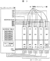
ディスク制御装置1は、ホストアダプタ部11と、ディスクアダプタ部12と、キャッシュメモリ部14を持ち、これらを接続するキャッシュメモリパス16を持つ。また、共有メモリ部15を有し、これとホストアダプタ部11とディスクアダプタ部12とを接続する共有メモリパス17を持っている。
The
ホストアダプタ部11は、ホストとインタフェースをおこなう部分であり、ホストコンピュータ50に対する入出力を制御する複数のプロセッサ6を有している。このホストアダプタ部11は、プロセッサ6の制御によりホストコンピュータ50とキャッシュメモリパス16を介してキャッシュメモリ部14のデータ転送を実行する。また、共有メモリ部15に対してもプロセッサ6の制御により共有メモリパス17を使用しデータを転送する。
The
ディスクアダプタ部12は、ディスク装置20とインタフェースをおこなう部分であり、ディスク装置20に対する入出力を制御するプロセッサ6を有し、プロセッサ6の制御によりディスク装置20とキャッシュメモリ部14間のデータ転送を実行する。ディスクアダプタ部12は、ディスクに対してのRAID制御等の演算機能の実行もおこなう。
The
また、共有メモリ部15に対してもマイクロプロセッサ6の制御により共有メモリ部15と接続する共有メモリパス17を使用しデータを転送する。
Also, data is transferred to the shared
ホストアダプタ部11、ディスクアダプタ部12は、共に、信頼性を向上させるために二重化されている。
Both the
キャッシュメモリ部14は、内部にメモリモジュール9を有し、ホストコンピュータ50とディスク装置20とでやり取りされるデータを一時的に保持する部分である。。
The
共有メモリ部15は、内部にメモリモジュール9を有し、キャッシュデータの管理情報を格納する。すなわち、複数のホストアダプタ部11、あるいは、複数のドライブアダプタ部12のキャッシュメモリへのアクセスについてデータ更新の排他制御等で必要なテーブル情報等を格納する。共有メモリデータがキャッシュメモリデータと違って、容量も小さく、トランザクション的なアクセスが多くレスポンス時間が短いことが性能向上に不可欠なためプロトコル・オーバーヘッド時間を少なくする必要がある。キャッシュメモリ部と共有メモリ部を分離した経路を持つ意味は、このようにデータアクセスの性質が相異なることを考慮しているためであり、キャッシュメモリ部14と共有メモリ部15とは耐故障性を考慮して、二重化されていることが一般的である。また装置電源断時のデータ保持のために従来装置(図10参照)のようにバッテリによる電源バックアップをしていることが通例である。
The shared
本発明のディスク制御装置は、不揮発メモリを、三つの異なる形態で用いている。 The disk controller of the present invention uses a nonvolatile memory in three different forms.
不揮発メモリ部8aは、キャッシュメモリ部14あるいは共有メモリ部15と従属した接続形態である。
The
不揮発メモリ部8bは、共有メモリパスに直接接続した形態である。
The
不揮発メモリ部8cは、HDDディスク配列の一部として接続した形態である。 The nonvolatile memory unit 8c is connected as part of the HDD disk array.
不揮発メモリ部8aは、キャッシュメモリ部14あるいは共有メモリ部15と従属した接続をしており、各々でキャッシュメモリデータあるいは共有メモリデータの移送を可能としたものである。したがって、電源断が発生する直前にデータを退避させるようにしておけば、バッテリによる電源バックアップをおこなわなくてもデータの保全が図れることになる。
The
また、通電時にはキャッシュバックする際のディスクへの書きこみをおこなう前に一時的エリアとしてデータの一部を書きこむこともできる。これはディスクにデータを置くよりも次の読み込みが早いという利点をもつ。 In addition, when energized, a part of data can be written as a temporary area before writing to the disk when cashing back. This has the advantage that the next read is faster than putting the data on the disk.
不揮発メモリ部8bは、ホストアダプタ部11とディスクアダプタ部12に共有メモリパス17を介して接続する。
The
この不揮発メモリ部8bは、不揮発メモリ部8aと違い独立した記憶エリアとして機能し、複数のプロセッサ6からアクセスされるメモリである。用途としては、システムの構成・管理情報を格納したり、マイクロプロセッサを実行するためのプログラムを格納したり、ディスクへのアクセス情報、障害ログ情報などを書きこみ保存することなどが考えられる。
The
不揮発メモリ部8cは、HDDディスク配列の一部のメディアデバイスとして用いられるものであり、ディスクに故障がおこったときの交替用の予備デバイスとして用いることができる。 The nonvolatile memory unit 8c is used as a part of the media device of the HDD disk array, and can be used as a spare device for replacement when a failure occurs in the disk.
また、ディスク装置20のすべてを、不揮発メモリ部8cによる配列にするという構成も考えられる。 A configuration in which all of the disk devices 20 are arranged by the nonvolatile memory unit 8c is also conceivable.
これら不揮発メモリ部8a,8b,8cらは、容量の拡張が可能とし、交換可能なように実装する。
These
また、不揮発メモリの特性を考慮して、書きこみ回数等の制限を管理し、デバイスの不良を検出できるようにする。そして、メモリモジュールを複数のメモリデバイスで構成し、不良なメモリデバイスの交換をおこなえるようにする。 In addition, in consideration of the characteristics of the nonvolatile memory, the limitation on the number of writings is managed so that a device failure can be detected. Then, the memory module is composed of a plurality of memory devices so that defective memory devices can be replaced.
さらに、これらの不揮発メモリ部に、メモリの障害検出とデータの保全のために、意図的に読み出してリライトする機能をもたせる。 Furthermore, these nonvolatile memory units are provided with a function of intentionally reading and rewriting for memory failure detection and data integrity.
すなわち、領域管理テーブルと更新来歴のマッピング情報等についての情報を内部レジスタ(ブロック管理用レジスタ)に持たせ、定期的に指定エリアに対し、アクセスのないときにリライトチェックをおこなう。そして、その書きこみ時には該当領域をロックさせ、上位からの更新を抑止させる。あるいは、上位からの更新要求があったときには、このリライト処理を中断させて、ロックを外し要求を完了後に、再度ロックしリライト処理するようにしてもよい。 That is, information on the area management table and update history mapping information and the like is provided in an internal register (block management register), and a rewrite check is periodically performed when there is no access to the designated area. Then, at the time of writing, the corresponding area is locked, and updates from the upper level are suppressed. Alternatively, when there is an update request from a host, this rewrite process may be interrupted, the lock may be released, and after the request is completed, the rewrite process may be performed again.
〔不揮発メモリ部の詳細〕
次に、図2ないし図9を用いてディスク制御装置内の不揮発メモリ部の詳細について説明する。
図2は、不揮発メモリ部のブロック図である。
図3は、不揮発メモリ部内のメモリコントローラとメモリモジュールのインタフェースを説明するための図である。
図4は、不揮発メモリ部のアドレス空間の説明図である。
図5は、パリティデータによるデータ復元の原理を説明するための図である。
図6は、不揮発メモリ内で保持されるデータ構造の模式図である。
図7は、不揮発メモリ部の不良ブロックの取扱いのイメージ図である。
図8は、不揮発メモリ部のデバイス交換後のデータ復元の概要を示す図である。
図9は、共有メモリ部の構成図である。
(I)不揮発メモリ部の構成概要
不揮発メモリ部8a,8b,8cの構成は、図2に示されるようにI/Fアダプタ部30とメモリコントローラ31と不揮発メモリモジュール32の主たる部位に分けられる。
(II)I/Fアダプタ部
I/Fアダプタ部30は、接続する装置内部のパスからの不揮発メモリモジュールへのデータ受信・送信に際し、インターフェースを解読し、内部の不揮発メモリモジュール32へのアクセスをメモリコントローラ部31の指揮下で制御する。
[Details of non-volatile memory]
Next, details of the nonvolatile memory unit in the disk controller will be described with reference to FIGS.
FIG. 2 is a block diagram of the nonvolatile memory unit.
FIG. 3 is a diagram for explaining an interface between a memory controller and a memory module in the nonvolatile memory unit.
FIG. 4 is an explanatory diagram of the address space of the nonvolatile memory unit.
FIG. 5 is a diagram for explaining the principle of data restoration using parity data.
FIG. 6 is a schematic diagram of a data structure held in the nonvolatile memory.
FIG. 7 is an image diagram of handling of defective blocks in the nonvolatile memory unit.
FIG. 8 is a diagram showing an outline of data restoration after device replacement in the nonvolatile memory unit.
FIG. 9 is a configuration diagram of the shared memory unit.
(I) Outline of Configuration of Nonvolatile Memory Unit The configuration of the
(II) I / F adapter unit The I / F adapter unit 30 decodes the interface and accesses the internal
すなわち、I/Fアダプタ部30は、上位I/Fパス9と接続し、それぞれのインターフェースのプロトコルを解析し、制御信号をメモリコントローラ部に提供する。ここで、接続する上位I/Fパス9の種類は、不揮発メモリ部8aであれば内部パス、不揮発メモリ部8bであれば、キャッシュメモリパス16、共有メモリパス17、そして不揮発メモリ部8cであればドライブI/F2である。
That is, the I / F adapter unit 30 is connected to the upper I /
I/Fアダプタ部30内のアダプタ制御部302を、このユニットを接続するI/Fに合わせて変更することで8a,8b,8cのバリエーションが作成できる。
I/Fアダプタ部では、接続パス9から送られるデータは、アダプタ制御部302のコントロールにより、I/Fアダプタ部30内で接続するパケットバッファ301で受信する。また、メモリモジュール33からの送信データをパケットバッファ301より送信する。
In the I / F adapter unit, the data sent from the
アダプタ制御部内にあるアドレス/コマンド解析部302aは、図示しなかったが、アドレスおよびコマンドを格納するバッファと、アドレス抽出部と、コマンド抽出部を有する。アドレス抽出部およびコマンド抽出部がその解析結果により、メモリコントローラ部31に対して制御信号を送信する。
(III)不揮発メモリ部8aの場合の接続するメモリ部の構成
不揮発メモリ部8aの場合は、図1のキャッシュ部14と共有メモリ部15に対して接続パスを設ける必要がある。したがって、この場合には、キャッシュ部14と共有メモリ部15の内部のパス制御を変更する必要がある。
Although not shown, the address /
(III) Configuration of Memory Unit to be Connected in the Case of
すなわち、共有メモリ部15の内部に、図9に示されるように、不揮発メモリパス18を設けるようにする。(また、キャッシュメモリ部14の場合も、おおよそ同様にして実現することができる。)
以下、共有メモリ部15の構成について説明する。
That is, the nonvolatile memory path 18 is provided inside the shared
Hereinafter, the configuration of the shared
共有メモリ部15は、複数のメモリモジュール159を有し、パスI/F部150と、パケットバッファ153と、データのエラーチェック部150と、メモリ制御部157と、アドレス/コマンド解析部155と、データ転送制御部152とを有している。
The shared
パケットバッファ153は、セレクタ156とデータを一時格納する部分である。メモリ制御部157は、メモリモジュール159へのアクセスを制御する部分である。アドレス/コマンド解析部155は、共有メモリパス17から送出されたアドレスおよびコマンドを解析する。
The packet buffer 153 is a part for temporarily storing the selector 156 and data. The
データ転送制御部152は、アービタ158により、アドレス/コマンド解析部155で解析した共有メモリパス17からのアクセス要求と、共有メモリ部に接続する不揮発メモリパス18からアクセス要求とのアービトレーションをおこない、セレクタ156の切り替えをおこなう。この不揮発メモリパス18からのアクセス要求があるのが本発明の特有の部分である。
The data
アドレス/コマンド解析部155は、バッファとアドレス抽出部とコマンド抽出部を有する(図示せず)。アドレス/コマンド解析部155では、共有メモリパス17に割り当てられたバッファに、アドレス、コマンドを格納する。(このパスは図9では4つ独立した系が示されている。)アドレス抽出部およびコマンド抽出部では、アクセスするメモリのアドレスとアクセスの種類を割り出し、メモリ制御部157へ送出する。また共有メモリパス17からのアクセス要求をデータ転送制御部152内のアービタ158へ送出する。このとき、通常はメモリモジュール159へのアクセスをおこなうが、不揮発メモリ部へのアクセスモードの場合はセレクタ156を切り替え、パスI/F部151と接続する不揮発メモリパス18へ切り替えを実施する。
The address /
またデータ転送制御部152には、ホストI/F部、ドライブI/F部の介在による共有メモリアクセスに依存せずに、共有メモリモジュール158のデータをダイレクトに不揮発メモリパス18へ転送する機能を持たせるようにする。
Further, the data
これは、緊急的に共有メモリデータを不揮発メモリ部へ転送する際に、時間を短縮するために有効な機能である。 This is an effective function for shortening the time when urgently transferring the shared memory data to the nonvolatile memory unit.
この機能は、通常の転送マスタはホストI/F部、ドライブI/F部であるが、この場合にセレクタ156の制御により転送マスタにデータ転送制御部152がなることで実現することができる。
(IV)メモリコントローラ部
メモリコントローラ部31は、エラーチェック回路部311と、送信バッファ312と、送受信セレクタ313とを有しており、これらは、不揮発メモリモジュール部32に接続パスを有している。
This function can be realized by having the data
(IV) Memory Controller Unit The
同様にI/Fアダプタ部への送信パスは、セレクタ部313から接続され、その間にエラーチェック回路部311が存在する。
Similarly, the transmission path to the I / F adapter unit is connected from the
メモリ制御部314は、不揮発メモリモジュール部32への制御線をコントロールしており、先に説明したI/Fアダプタ部30内のコマンドアドレス解析部302からの制御線からの信号により、送信バッファ312とセレクタ部313への信号を出力する。このメモリ制御部は、アクセスされる論理アドレスを、内部の物理アドレスに変換するアドレス変換機能と、アクセスするアドレス毎にプロテクトをおこなうロック機能を有している。
The
また、VPP制御部315は、不揮発EEPROM等のメモリモジュールの書きこみ電源の制御等で必要な場合機能をさせる。
Also, the
このメモリ制御部314は、不揮発メモリモジュール32内の複数の不揮発メモリ配列に対してアクセスを制御し、データ保証のための演算回路316を有する。
This
この演算回路316は、パリティデータや保護コードからデータ復元をおこなう回路であり、これらについては後に詳細に説明する。
(V)不揮発メモリモジュール部
不揮発メモリモジュール部32は、図2に示されているように複数のメディアの配列を構成要素として持っている。これは単体メディアの保守を可能とするためで、故障あるいは保守対象メディアを示すインジケータ(LED等)により、その部位のインジケータがONであるときに交換保守できるようになっている。また、メディアを容量の違うタイプに交換してアップグレードすることを許容とした構造を持っている。
The
(V) Nonvolatile Memory Module Unit The nonvolatile
不揮発メモリモジュール部32に実装されるメモリデバイスは、データ格納用、データ格納用スペア、パリティデータ格納用の三種類である。
(VI)メモリコントローラと不揮発メモリモジュールのインターフェース
次に、図3を用いてメモリコントローラ31と不揮発メモリモジュール32のインターフェースについて説明する。
There are three types of memory devices mounted on the nonvolatile memory module unit 32: data storage, data storage spare, and parity data storage.
(VI) Interface between Memory Controller and Nonvolatile Memory Module Next, an interface between the
図3では、メモリコントローラ部31と5つのメモリモジュール部32が接続されている。各々のデータは、ADRESS/DATAバスにて送受信され、デバイスの選択はチップイネーブル(CE)信号がアサートされて実現する。またライトイネーブル(WE)信号、アウトプットイネーブル(OE)信号は、書きこみ/読み込みかを選択し、CLK信号等により同期をとりデバイスに書きこみ/リードする。
(VII)不揮発メモリ部のアドレス空間
ADRESSデータ信号、物理アドレス空間は、コントローラ内部のアドレステーブルで論理アドレスから物理アドレスに変換される間接アドレッシング方式を使用する。これにより、論理的にアクセスできるアドレス空間は拡張される。
In FIG. 3, a
(VII) Address Space of Non-Volatile Memory Unit The ADDRESS data signal and physical address space use an indirect addressing system in which a logical address is converted into a physical address in an address table inside the controller. As a result, the logically accessible address space is expanded.
アドレス空間は、図4のイメージのように拡張空間によりデバイスの容量増加に対応できるしくみとなる。すなわち、実データとブロックはページに格納され、そのページが集まってフレームを構成する。 As shown in the image of FIG. 4, the address space is a mechanism that can cope with the increase in the capacity of the device by the expansion space. That is, actual data and blocks are stored in a page, and the pages gather to form a frame.
論理アドレスから物理アドレスの変換は、内部のアドレステーブルによりデバイスの物理アドレスに間接的にリンクさせるものである。またメモリ制御部31内に設けたレジスタにではなく、アドレステーブルをデバイスの固定エリアに書きこみ、その固定エリアをアクセスして、その情報を一度に読みこんでアドレス演算できるようにする方法も考えられる。
The conversion from the logical address to the physical address is to indirectly link to the physical address of the device by an internal address table. A method is also conceivable in which an address table is written in a fixed area of the device, not in a register provided in the
論理アドレスにより、アクセスする利点は、外部から内部の物理構造などを意識せずにインタフェースの設計ができることである。
(VIII)プロテクト機能と書きこみ回数のカウント
不揮発メモリ部でアクセスされるメモリは、ブロック毎にライト/リードプロテクト(ロックする)機能を持たせるようにする。これは、書き換えが許されないデータを保護のするためと、メモリの回復処理中で、元データによりそのアドレスの内容を復元しているときに、他のアクセスによってデータが修正されないようにするためにも必要な機能である。また、不揮発メモリ部8bにプロセッサのプログラムを格納するときのように、読み取りの性格が強いデータを格納する目的で使用している場合にも、ライトプロテクトを意識して制御することは大切である。
The advantage of accessing with a logical address is that the interface can be designed from outside without being aware of the internal physical structure.
(VIII) Protect function and count of the number of write operations The memory accessed in the nonvolatile memory section should have a write / read protect (lock) function for each block. This is to protect data that cannot be rewritten, and to prevent data from being modified by other accesses when the contents of the address are being restored by the original data during the memory recovery process. Is also a necessary function. It is also important to control with the write protection in mind when the data is used for storing data with a strong read characteristic, such as when storing a processor program in the
また、内部にデバイスに含まれるブロックごとに、書きこみ回数カウンタを構成し、書きこみ実施完了後にカウント値を+1させる。そしてカウンタ値があらかじめ指定した閾値(しきいち)を超えた場合は、自動的にライトプロテクトする機能を持たせるようにする。あるいは、前もって交換ワーニングを示すようにしてもよい。これにより不揮発メモリの書きこみ回数のチェックと保守交換時期の予測をおこなうことが可能となる。 In addition, a writing number counter is configured for each block included in the device, and the count value is incremented by 1 after writing is completed. When the counter value exceeds a predetermined threshold value (Shikiichi), a function of automatically performing write protection is provided. Alternatively, the replacement warning may be indicated in advance. This makes it possible to check the number of times of writing to the nonvolatile memory and predict the maintenance replacement time.
また、書きこみ回数については、内部の回路に情報格納用のレジスタを設ける方法と、不揮発メモリ自体にデータを保存する方法が考えられる。アドレス変換のための情報も同様に不揮発メモリ自体に保存しておくことも可能である。 Regarding the number of times of writing, there are a method of providing a register for storing information in an internal circuit and a method of saving data in the nonvolatile memory itself. Similarly, information for address conversion can be stored in the nonvolatile memory itself.
さらに、アドレステーブルの障害に対応するために、二重にデータをコントローラ部内レジスタとデバイス自体に格納するという方法もとることも選択できる。
(IX)不揮発メモリ部への通常のアクセス
不揮発メモリ部へのデータの格納はブロック単位に実行される。図2の送信バッファ312の容量サイズは、複数のブロック容量が入るサイズであり、またデバイスごとに専用のバッファが設けられることが望ましい。不揮発メモリデバイス、例えば、不揮発EEPROMなどは、イレーズ(消去)して書きこまなくてはならないものもあり、ライトアクセス処理時間がリードに比べて遅いという特性がある。その欠点を補うために、データが来たときに、送信バッファ312に、複数ブロックを格納して、アダプタ部30が上位側への応答をすれば、デバイスへのライト処理をおこなう場合の、見かけ上のアクセス時間を短くすることができる。
Furthermore, in order to cope with a failure in the address table, it is possible to select a method of storing data in the controller unit register and the device itself twice.
(IX) Normal access to the nonvolatile memory unit Data is stored in the nonvolatile memory unit in units of blocks. The capacity size of the
また、複数のデバイスを並列に書き込み/読み込みすることによっても、転送スループットが向上できる。並列に実装される例としては、図3に示されており、これによると、不揮発メモリモジュール部32は、データ格納用にD3、D2、D1とパリティデータ用Q、そしてこれらが使用不能となり、さらに交換不能となった場合のスペアロケーションSPが予備として配列されている。
(X)パリティデータ
次に、図5を用いて本発明の不揮発メモリデバイスに用いられるパリティデータによるデータ復元の原理について説明する。
Also, the transfer throughput can be improved by writing / reading a plurality of devices in parallel. An example implemented in parallel is shown in FIG. 3, according to which the non-volatile
(X) Parity Data Next, the principle of data restoration using parity data used in the nonvolatile memory device of the present invention will be described with reference to FIG.
パリティデータとは、冗長データであり、図5(a)の例でいえば、D3からD1の排他的論理和演算結果としてQのデータを生成する。 Parity data is redundant data. In the example of FIG. 5A, Q data is generated as an exclusive OR operation result from D3 to D1.
復元についても、図5(b)の例に示すとおり、パリティデータQと正常なデバイスデータD3、D1の排他的論理和を演算すると復元データが計算できる。 As for the restoration, as shown in the example of FIG. 5B, the restoration data can be calculated by calculating the exclusive OR of the parity data Q and the normal device data D3 and D1.
この排他的論理和演算は、ビット毎に演算されているため、パリティデータによる当該ビットを復元することが可能となる。
(XI)保守と障害発生時の回復プロセス
次に、本発明の不揮発メモリ部の保守と障害がおこったときに、どのようにデータを復元して回復させるかについて説明する。
Since this exclusive OR operation is performed for each bit, it is possible to restore the bit based on the parity data.
(XI) Maintenance and Recovery Process When Failure Occurs Next, how to restore and recover data when maintenance and failure of the nonvolatile memory unit of the present invention occur will be described.
不揮発メモリモジュール部32のメモリデバイスに対してはブロック単位にデータを分割して格納する。
In the memory device of the nonvolatile
データは、図6に示したように、D3、D2、D1に格納されるブロックデータとパリティのデータのトータルを1ページとし、複数ページを1フレームとしてデータを管理している。 As shown in FIG. 6, the data is managed with the total of block data and parity data stored in D3, D2, and D1 as one page and a plurality of pages as one frame.
D3、D2、D1に格納される単位のブロックデータは、複数バイトサイズの実データと、ブロック固有のブロックコードから構成されている。 The unit block data stored in D3, D2, and D1 is composed of real data having a plurality of bytes and a block code unique to the block.
そして、ブロック固有のブロックコードは、ブロックデータの固有ID番号(Logical ID)と、デバイス上にて該当ブロック領域が何回書きこまれたかの履歴である更新回数(Write Number、以下「WN」と記す)とそのデータから演算されるCRC等のデータ保護コードから構成されており、このブロックコードをチェックすることで、正しいロケーションに正しいデータが保存されていること、また、更新回数が不揮発メモリの限界回数値より低い規定値を満たしているかを判断できる。 The block code unique to the block is described as a unique ID number (Logical ID) of the block data and an update count (Write Number, hereinafter referred to as “WN”) that is a history of how many times the corresponding block area has been written on the device. ) And a data protection code such as CRC calculated from the data. By checking this block code, the correct data is stored in the correct location, and the number of updates is limited by the nonvolatile memory. It can be judged whether the specified value lower than the number of times is satisfied.
このチェックにより障害が発見されたブロックデータに関しては、スペアロケーションに対してアクセスを切り替えるようにする。その際、LI番号は故障したブロックの番号を引き継ぎ、WNはスペアロケーションの該当ブロックに対する値に更新する。図7が障害ブロックデータをスペアロケーションデバイスに交替例を示している。 For block data in which a failure is found by this check, the access is switched to the spare location. At that time, the LI number takes over the number of the failed block, and the WN is updated to a value for the corresponding block in the spare location. FIG. 7 shows an example of replacing failed block data with a spare location device.
交替ブロックの数が一定以上になった場合には、そのデバイスが相当劣化していることが考えられる。そのために、保守している者に対してデバイス交換を示唆するために、制御部31内にある管理情報のレジスタに報告し、ワーニングとして、インジケータやアラームを点灯させる。不良デバイスの交換に際しては、障害が発生するとただちに不揮発メモリ部への書きこみを、いったん停止して、該当エリアに対しての論理的アドレスをライトロックし、あるいは、リードロックさせる。
If the number of replacement blocks exceeds a certain level, it is possible that the device has deteriorated considerably. Therefore, in order to suggest the device replacement to the person who is maintaining, it is reported to the management information register in the
そして、不良デバイスを新しい正常なデバイスに交換した後、図8に示すように、スペアデバイス内の交替データを複写し、スペアデバイスに交替データがないブロックは、D3、D1、Qよりデータを読み込み、(X)で説明したパリティ演算をおこなうことによりデータを復元させる。 Then, after replacing the defective device with a new normal device, as shown in FIG. 8, the replacement data in the spare device is copied, and the block having no replacement data in the spare device reads the data from D3, D1, and Q. The data is restored by performing the parity calculation described in (X).
この際、新しいデバイスの更新データは、初期値にリセットされ、スペアデバイスは複写ブロックデータは消去されるがWNは更新される。故障デバイスを交換したら、そのことを制御信号(図3のSY/RY)により感知し、自動的に回復処理をさせることもできる。データパリティ演算により復元したデータとスペアデバイスに交替したブロックデータを新しいデバイスに格納し、そのデバイスが回復したことが確認できたら、インジケーターLEDを正常な状態に表示する。 At this time, the update data of the new device is reset to the initial value, and the copy block data is deleted from the spare device, but the WN is updated. When a failed device is replaced, this can be detected by a control signal (SY / RY in FIG. 3), and a recovery process can be automatically performed. The data restored by the data parity calculation and the block data replaced with the spare device are stored in a new device, and when it is confirmed that the device has been recovered, the indicator LED is displayed in a normal state.
また不揮発メモリは、データが不揮発であるという前提ではあるが、半導体のソフトエラー等の経年変化によるデータの消失の可能性が全くないとは言えず、いざ読み込んだ際にデータがエラーになってしまう場合や、あるいは書きこみ回数が許容値に近づいていることが懸念される。 Non-volatile memory is based on the premise that data is non-volatile, but it cannot be said that there is no possibility of data loss due to secular changes such as semiconductor soft errors. There is a concern that the number of times of writing or the number of times of writing is approaching an allowable value.
前もって保守交換のためのチェックは、システムを安定に運営する上でも必要であり、定期的にリライトすることが効果的である。定期的リライトモードにより、読み書きチェックをページ/ブロック単位におこなう回路をメモリコントローラ314に内蔵させる(図示していない)。リライトモードはアドレス範囲の設定とリライトモードコマンドの発行によってスタートされる。データバッファに読み出し、そのデータをもとの場所に書きこむ制御をする。 Checks for maintenance replacement in advance are also necessary for stable operation of the system, and it is effective to rewrite regularly. In the periodic rewrite mode, a circuit for performing a read / write check for each page / block is built in the memory controller 314 (not shown). The rewrite mode is started by setting an address range and issuing a rewrite mode command. Controls reading to the data buffer and writing the data to the original location.
使用されていないとき、あるいは、強制的にロックしたエリアのみこのリライトチェックをおこなうようにする。このリライトチェックでは、リライトした後読み出しを実施し、パリティ演算回路で排他的論理和演算しデータを比較することにより、再度チェックをおこなう。また、保護コードのみをチェック対象として検査のためのオーバヘッドを減らすことも可能である。 This rewrite check is performed only when the area is not in use or forcibly locked. In this rewrite check, reading is performed after rewriting, an exclusive OR operation is performed by a parity operation circuit, and the data is compared to perform the check again. It is also possible to reduce the overhead for inspection by checking only the protection code.
故障の保守対象デバイスはインジケートするインジケーターとしてのLEDの点灯によって保守員がわかるようにし、書きこみ回数カウンター値等により、規定回数以上を検出、エラー情報をメモリコントローラ内のエラーレジスタにモニタさせたり、LEDの点灯をさせるようにする。LEDが点灯し、その部位のアクセスをロックさせ、保守の交換までそのデバイスにアクセスさせないようにする。故障デバイスを交換したら、そのことを制御信号(図3のSY/RY)により感知し、自動的に回復処理をさせることもできる。データパリティ演算により補間したデータが回復したことが確認できたら、インジケーターLEDを正常な状態に表示する。 The maintenance target device of the failure can be identified by the lighting of the LED as an indicator to indicate, and the number of times more than the specified number is detected by the write count counter value, etc., and the error information in the memory controller is monitored. Let the LED light up. The LED illuminates, locking the site access and preventing access to the device until maintenance replacement. When a failed device is replaced, this can be detected by a control signal (SY / RY in FIG. 3), and a recovery process can be automatically performed. When it is confirmed that the interpolated data has been recovered by the data parity calculation, the indicator LED is displayed in a normal state.
〔ディスク制御装置に不揮発メモリを使用したことの利点〕
不揮発メモリは、フラッシュEEPROMに代表されるように、現在は、HDDより容量は小さいが年々コストが安くなり、デバイス当りの容量も増加している。HDDのように機械的な部品もなく、実装スペースならび消費電力の小さい点で記憶デバイスとして有利な点を持っている。
[Advantages of using non-volatile memory for disk controller]
As represented by a flash EEPROM, a nonvolatile memory has a capacity smaller than that of an HDD, but its cost is decreasing year by year, and the capacity per device is also increasing. There is no mechanical part like HDD, and it has an advantage as a storage device in terms of mounting space and low power consumption.
本発明は、ディスク記憶制御装置の中で部分的に不揮発メモリ部を記憶領域として使用するようにした。記憶装置のデータの一部を格納しキャッシュメモリ部の揮発メモリに対してバックアップ電源としてバッテリをもたせる代わりに不揮発メモリに緊急避難させることでき、バッテリの容量を減らし、装置の消費する電力を削減することができる。 In the present invention, a nonvolatile memory part is partially used as a storage area in the disk storage control device. Instead of storing a part of the data in the storage device and having a battery as a backup power source for the volatile memory in the cache memory unit, emergency evacuation can be made to the nonvolatile memory, reducing the capacity of the battery and reducing the power consumed by the device be able to.
また、不揮発メモリデバイスを複数配列しているので、故障したデバイス単位に保守でき、HDDを解体して中の円盤等の修理をするより、不揮発メモリデバイスのみを交換保守するので、修理時間が短く修理コストも安くなる。2次記憶領域として、あるいは、HDDに代わる記憶デバイスとして、装置の低価格化、消費電力の削減、保守性の向上に貢献することが期待できる。 In addition, since multiple non-volatile memory devices are arranged, maintenance can be performed on a failed device basis, and only the non-volatile memory device is replaced and maintained rather than dismantling the HDD and repairing the disk inside. Repair costs are also reduced. As a secondary storage area or as a storage device that replaces the HDD, it can be expected to contribute to the reduction in the price of the apparatus, the reduction in power consumption, and the improvement in maintainability.
1…ディスク制御装置、2…ドライブI/F、3…ホストI/F、4…キャッシュメモリ制御部、5…共有メモリアクセス制御部、6…マイクロプロセッサ部、8a…不揮発メモリ部、8b…不揮発メモリ部、8c…不揮発メモリ部、9…メモリモジュール、10…バッテリ部、11…ホストアダプタ部、12…ディスクアダプタ部、13…不揮発メモリパス、14…キャッシュメモリ部、15…共有メモリ部、16…キャッシュメモリパス、17…共有メモリパス、20…磁気ディスクデバイス部、30…I/Fアダプタ部、301…パケットバッファ、302…アダプタ制御部、302a…コマンド/アドレス解析部、31…メモリコントローラ部、311…エラーチェック回路部、312…送信バッファ、313…セレクタ、314…メモリ制御部、315…VPP制御部、316…演算回路、32…不揮発メモリモジュール部、40…共有メモリメモリパス、150…エラーチェック回路部、151…パスI/F部、152…データ転送制御部、153…パケットバッファ、155…アドレスコマンド解析部、157…メモリ制御部、158…アービタ、159…メモリモジュール、50…ホストコンピュータ。
DESCRIPTION OF
Claims (15)
前記ホストインタフェース部に接続され、前記計算機からアクセスされるデータを格納するキャッシュメモリ部と、
前記ホストインタフェース部および前記キャッシュメモリ部に接続され、前記計算機からアクセスされるデータの入出力を制御するディスクインタフェース部と、
前記ディスクインタフェース部に接続され、前記計算機からアクセスされるデータを格納する複数のディスク装置とを有し、
前記ディスクインタフェース部に接続され、前記計算機からアクセスされるデータを格納するフラッシュメモリ部とを有し、
前記ディスクインタフェース部は、第1、第2のディスクインタフェース部から構成され、前記第1のディスクインタフェース部に接続される複数の第1の通信路と、前記第2のディスクインタフェース部に接続される複数の第2の通信路とを有し、
前記フラッシュメモリ部は、前記複数のディスク装置の交替用の記憶媒体であり、
前記複数のそれぞれの第1の通信路には、少なくとも1つの前記ディスク装置および前記フラッシュメモリ部が接続され、前記複数の第2の通信路には、それぞれ、前記第1の通信路に接続された少なくとも一つの前記ディスク装置および前記フラッシュメモリ部が接続されることを特徴とするストレージシステム。 A host interface connected to the computer;
A cache memory unit connected to the host interface unit and storing data accessed from the computer;
A disk interface unit connected to the host interface unit and the cache memory unit and controlling input / output of data accessed from the computer;
A plurality of disk devices connected to the disk interface unit and storing data accessed from the computer;
A flash memory unit connected to the disk interface unit and storing data accessed from the computer;
The disk interface unit includes first and second disk interface units, and is connected to a plurality of first communication paths connected to the first disk interface unit and the second disk interface unit. A plurality of second communication paths,
The flash memory unit is a storage medium for replacement of the plurality of disk devices,
At least one of the disk device and the flash memory unit is connected to each of the plurality of first communication paths, and each of the plurality of second communication paths is connected to the first communication path. A storage system, wherein at least one of the disk device and the flash memory unit are connected.
前記ホストインタフェース部に接続され、前記計算機からアクセスされるデータを格納するキャッシュメモリ部と、
前記ホストインタフェース部および前記キャッシュメモリ部に接続され、前記計算機からアクセスされるデータの入出力を制御するディスクインタフェース部と、
前記ディスクインタフェース部に接続され、前記計算機からアクセスされるデータを格納する複数のディスク装置と、
前記ディスクインタフェース部に接続され、前記計算機からアクセスされるデータを格納する不揮発メモリ部とを有し、
前記不揮発メモリ部は、インタフェースアダプタ部と、データを格納する複数の不揮発メモリデバイスと、前記複数の不揮発メモリデバイスに対するデータの書込み又は読み出しを制御するコントローラ部とを有し、
前記インタフェースアダプタ部は、前記ディスクインタフェース部との間で用いられるプロトコルを解析し、前記ディスクインタフェース部から送信される制御信号およびデータを前記コントローラ部に送信し、前記コントローラ部は、前記制御信号により前記データをエラーチェックし、前記複数の不揮発メモリデバイスに書き込むことを特徴とするストレージシステム。 A host interface connected to the computer;
A cache memory unit connected to the host interface unit and storing data accessed from the computer;
A disk interface unit connected to the host interface unit and the cache memory unit and controlling input / output of data accessed from the computer;
A plurality of disk devices connected to the disk interface unit for storing data accessed from the computer;
A non-volatile memory unit that is connected to the disk interface unit and stores data accessed from the computer;
The nonvolatile memory unit includes an interface adapter unit, a plurality of nonvolatile memory devices that store data, and a controller unit that controls writing or reading of data with respect to the plurality of nonvolatile memory devices,
The interface adapter unit analyzes a protocol used with the disk interface unit, transmits a control signal and data transmitted from the disk interface unit to the controller unit, and the controller unit receives the control signal according to the control signal. An error check is performed on the data, and the data is written to the plurality of nonvolatile memory devices.
前記ディスクインタフェース部は、第1、第2のディスクインタフェース部であり、
前記第1のディスクインタフェース部に接続される複数の第1の通信路と、
前記第2のディスクインタフェース部に接続される複数の第2の通信路とを有し、
前記複数のそれぞれの第1の通信路には、少なくとも1つの前記ディスク装置および前記不揮発性メモリ部が接続され、前記複数の第2の通信路には、それぞれ、前記第1の通信路に接続された少なくとも一つの前記ディスク装置および前記不揮発性メモリ部が接続されることを特徴とするストレージシステム。 The storage system according to claim 2,
The disk interface unit is a first and second disk interface unit,
A plurality of first communication paths connected to the first disk interface unit;
A plurality of second communication paths connected to the second disk interface unit,
At least one of the disk device and the nonvolatile memory unit is connected to each of the plurality of first communication paths, and each of the plurality of second communication paths is connected to the first communication path. A storage system, wherein the at least one disk device and the nonvolatile memory unit are connected.
前記ホストインタフェース部に接続され、前記計算機からアクセスされるデータを格納するキャッシュメモリ部と、
前記ホストインタフェース部および前記キャッシュメモリ部に接続され、前記計算機からアクセスされるデータの入出力を制御するディスクインタフェース部と、
前記ディスクインタフェース部に接続され、前記計算機からアクセスされるデータを格納する複数のディスク装置と、
前記ディスクインタフェース部に接続され、前記計算機からアクセスされるデータを格納する不揮発メモリ部とを有し、
前記複数のディスク装置および不揮発メモリ部は、前記複数のディスク装置からなる記憶媒体の配列の一部としてRAID(Redundant Arrays of Inexpensive Disks)グループを構成し、
前記不揮発メモリ部は、前記複数のディスク装置のいずれかのディスク装置の交替用の予備記憶媒体であり、
前記RAIDグループに属する前記いずれかのディスク装置に障害が生じた場合、前記障害が生じたディスク装置に対する前記計算機からのアクセスを、前記RAIDグループに属する前記不揮発メモリ部に対するアクセスに切り替え、前記計算機から送受信されるデータを前記不揮発メモリ部に格納することを特徴とするストレージシステム。 A host interface connected to the computer;
A cache memory unit connected to the host interface unit and storing data accessed from the computer;
A disk interface unit connected to the host interface unit and the cache memory unit and controlling input / output of data accessed from the computer;
A plurality of disk devices connected to the disk interface unit for storing data accessed from the computer;
A non-volatile memory unit that is connected to the disk interface unit and stores data accessed from the computer;
The plurality of disk devices and the nonvolatile memory unit constitute a RAID (Redundant Arrays of Inexpensive Disks) group as a part of an array of storage media composed of the plurality of disk devices,
The nonvolatile memory unit is a spare storage medium for replacement of any one of the plurality of disk devices,
When a failure occurs in any of the disk devices belonging to the RAID group, the access from the computer to the disk device in which the failure has occurred is switched to the access to the nonvolatile memory unit belonging to the RAID group, and from the computer A storage system that stores data to be transmitted and received in the nonvolatile memory unit.
前記複数のディスク装置からなる記憶媒体の配列の一部として前記不揮発メモリ部を有することを特徴とするストレージシステム。 The storage system according to claim 4,
A storage system comprising the non-volatile memory unit as part of an array of storage media comprising the plurality of disk devices.
前記ディスクインタフェース部に接続される不揮発メモリ部は、前記キャッシュメモリ部に格納されるデータを格納することを特徴とするストレージシステム。 The storage system according to claim 4,
A non-volatile memory unit connected to the disk interface unit stores data stored in the cache memory unit.
当該ストレージシステム内で送受信される制御情報を格納する共有メモリ部を有し、
前記ディスクインタフェース部に接続される不揮発メモリ部は、前記制御情報を格納することを特徴とするストレージシステム。 The storage system according to claim 4,
Having a shared memory unit for storing control information transmitted and received in the storage system;
A non-volatile memory unit connected to the disk interface unit stores the control information.
前記ディスクインタフェース部に接続される不揮発メモリ部は、前記ディスクインタフェース部とに搭載されているマイクロプロセッサの実行するプログラムを格納することを特徴とするストレージシステム。 The storage system according to claim 4,
A non-volatile memory unit connected to the disk interface unit stores a program executed by a microprocessor mounted on the disk interface unit.
前記ディスクインタフェース部に接続される不揮発メモリ部は、前記計算機の前記ディスク装置に対するアクセスログ情報、障害ログ情報を格納することを特徴とするストレージシステム。 The storage system according to claim 4,
A non-volatile memory unit connected to the disk interface unit stores access log information and failure log information for the disk device of the computer.
前記ホストインタフェース部に接続され、前記計算機からアクセスされるデータを格納するキャッシュメモリ部と、
前記ホストインタフェース部および前記キャッシュメモリ部に接続され、前記計算機からアクセスされるデータの入出力を制御するディスクインタフェース部と、
前記ディスクインタフェース部に接続され、前記計算機からアクセスされるデータを格納する複数のディスク装置と、
前記ディスクインタフェース部に接続され、前記計算機からアクセスされるデータを格納する不揮発メモリ部とを有し、
前記不揮発メモリ部は、該不揮発メモリ部内に並列に実装される複数の不揮発メモリデバイスと、
前記複数の不揮発メモリデバイスに格納されるデータと、前記複数の不揮発メモリデバイスのうちのいずれかの不揮発メモリデバイスに格納されるパリティデータとを用いてデータ演算するコントローラとを有し、
前記複数の不揮発メモリデバイスは、それぞれ、最小ブロック単位ごとに、データと、該データの論理管理IDと、該最小ブロック単位の良、不良を判定するための保護コードと、更新時にインクリメントされる更新回数情報とを含み、
前記コントローラは、前記更新回数情報を監視し、前記更新回数情報が一定の閾値を超えた場合、該最少ブロック単位を不良ブロックとして前記保護コードを更新し、該最少ブロックに対応するデータを読み出してリライトすることを特徴とするストレージシステム。 A host interface connected to the computer;
A cache memory unit connected to the host interface unit and storing data accessed from the computer;
A disk interface unit connected to the host interface unit and the cache memory unit and controlling input / output of data accessed from the computer;
A plurality of disk devices connected to the disk interface unit for storing data accessed from the computer;
A non-volatile memory unit that is connected to the disk interface unit and stores data accessed from the computer;
The nonvolatile memory unit includes a plurality of nonvolatile memory devices mounted in parallel in the nonvolatile memory unit,
A controller that performs data operation using data stored in the plurality of nonvolatile memory devices and parity data stored in any one of the plurality of nonvolatile memory devices;
Each of the plurality of nonvolatile memory devices includes, for each minimum block unit, data, a logical management ID of the data, a protection code for determining whether the minimum block unit is good or bad, and an update incremented at the time of update Count information and
The controller monitors the update number information, and when the update number information exceeds a certain threshold, updates the protection code with the smallest block unit as a defective block, and reads data corresponding to the smallest block. A storage system characterized by rewriting.
前記不揮発メモリ部は、前記複数の不揮発メモリデバイスのそれぞれに対応するインジケータを有し、前記複数の不揮発メモリデバイスのうちの一の不揮発メモリデバイスに障害が生じた場合、該一の不揮発メモリデバイスの前記インジケータに表示し、該一の不揮発メモリデバイスは物理的に交換可能であることを特徴とするストレージシステム。 The storage system according to claim 10, wherein
The nonvolatile memory unit has an indicator corresponding to each of the plurality of nonvolatile memory devices, and when a failure occurs in one nonvolatile memory device of the plurality of nonvolatile memory devices, the nonvolatile memory device A storage system displayed on the indicator, wherein the one non-volatile memory device is physically replaceable.
前記一の不揮発メモリデバイスを交換する場合、前記不揮発メモリ部は、前記一の不揮発メモリデバイス内の復元対象のデータの最小ブロック単位が、前記複数の不揮発メモリデバイスのうちの他の不揮発メモリデバイスにスペアとして作成されているとき、該スペアの最小ブロック単位を交替ブロック単位とし、前記他の不揮発メモリデバイスにスペアとして作成されていないとき、前記複数の不揮発メモリデバイスのうちのいずれかのメモリデバイス内のデータおよびパリティデータを用いて、前記復元対象のデータの最小ブロック単位を作成して交替ブロック単位とし、前記交替ブロック単位を用いて前記復元対象のデータを復元することを特徴とするストレージシステム。 The storage system according to claim 10, wherein
When replacing the one non-volatile memory device, the non-volatile memory unit is configured such that the minimum block unit of data to be restored in the one non-volatile memory device is transferred to another non-volatile memory device of the plurality of non-volatile memory devices. When created as a spare, the smallest block unit of the spare is used as a replacement block unit, and when not created as a spare in the other nonvolatile memory device, the memory device in any one of the plurality of nonvolatile memory devices The storage system is characterized in that a minimum block unit of the restoration target data is created as a replacement block unit using the data and parity data, and the restoration target data is restored using the replacement block unit.
前記不揮発メモリ部は、該不揮発メモリ部内に格納されたデータの論理アドレスと物理アドレスとを対応付ける変換テーブルを有し、前記計算機から前記データに対する入出力要求がある場合、該テーブルを用いて、前記入出力要求に含まれる前記データの論理アドレスを物理アドレスに変換することを特徴とするストレージシステム。 The storage system according to claim 10, wherein
The non-volatile memory unit has a conversion table that associates the logical address and physical address of data stored in the non-volatile memory unit, and when there is an input / output request for the data from the computer, A storage system for converting a logical address of the data included in an entry output request into a physical address.
前記不揮発メモリ部は、前記複数の不揮発メモリデバイスの分割されたデータの最小ブロック単位ごとに、リードプロテクト、ライトプロテクトを実行することを特徴とするストレージシステム。 The storage system according to claim 10, wherein
The storage system, wherein the nonvolatile memory unit executes read protection and write protection for each minimum block unit of divided data of the plurality of nonvolatile memory devices.
前記不揮発メモリ部は、データバッファを有し、任意の契機に、前記複数の不揮発メモリデバイスのうちのある不揮発メモリデバイス内のある論理アドレスからデータを読み出して該データバッファに格納し、該データバッファに格納した前記データを前記論理アドレスに書き込み、前記データに対してリードプロテクトまたはライトプロテクトを実行した場合、前記論理アドレスに書き込んだ前記データと、前記複数の不揮発メモリデバイスのうちの他の不揮発メモリデバイス内のデータをパリティ演算して作成したデータとを比較して、不良ブロックを判定することを特徴とするストレージシステム。 15. The storage system according to claim 14, wherein
The nonvolatile memory unit has a data buffer, and at an arbitrary timing, reads data from a certain logical address in a nonvolatile memory device of the plurality of nonvolatile memory devices, stores the data in the data buffer, and stores the data buffer. When the data stored in the logical address is written to the logical address and read protection or write protection is executed on the data, the data written to the logical address and another nonvolatile memory of the plurality of nonvolatile memory devices A storage system characterized in that a bad block is determined by comparing with data created by performing parity operation on data in a device.
Priority Applications (1)
| Application Number | Priority Date | Filing Date | Title |
|---|---|---|---|
| JP2008097026A JP2008217811A (en) | 2008-04-03 | 2008-04-03 | Disk controller using nonvolatile memory |
Applications Claiming Priority (1)
| Application Number | Priority Date | Filing Date | Title |
|---|---|---|---|
| JP2008097026A JP2008217811A (en) | 2008-04-03 | 2008-04-03 | Disk controller using nonvolatile memory |
Related Parent Applications (1)
| Application Number | Title | Priority Date | Filing Date |
|---|---|---|---|
| JP2002178537A Division JP2004021811A (en) | 2002-06-19 | 2002-06-19 | Disk controller using nonvolatile memory |
Publications (2)
| Publication Number | Publication Date |
|---|---|
| JP2008217811A true JP2008217811A (en) | 2008-09-18 |
| JP2008217811A5 JP2008217811A5 (en) | 2009-05-14 |
Family
ID=39837700
Family Applications (1)
| Application Number | Title | Priority Date | Filing Date |
|---|---|---|---|
| JP2008097026A Pending JP2008217811A (en) | 2008-04-03 | 2008-04-03 | Disk controller using nonvolatile memory |
Country Status (1)
| Country | Link |
|---|---|
| JP (1) | JP2008217811A (en) |
Cited By (2)
| Publication number | Priority date | Publication date | Assignee | Title |
|---|---|---|---|---|
| JP2012523594A (en) * | 2009-08-31 | 2012-10-04 | 株式会社日立製作所 | Storage system having multiple flash packages |
| JP2014182460A (en) * | 2013-03-18 | 2014-09-29 | Fujitsu Ltd | Storage control apparatus, and storage system |
Citations (18)
| Publication number | Priority date | Publication date | Assignee | Title |
|---|---|---|---|---|
| JPS6072048A (en) * | 1983-09-02 | 1985-04-24 | インタ−ナショナル ビジネス マシ−ンズ コ−ポレ−ション | Memory corrector |
| JPH01269299A (en) * | 1988-04-20 | 1989-10-26 | Hitachi Ltd | Semiconductor memory device |
| JPH0325798A (en) * | 1989-06-23 | 1991-02-04 | Ricoh Co Ltd | Storage device using eeprom |
| JPH0498342A (en) * | 1990-08-09 | 1992-03-31 | Mitsubishi Electric Corp | Semiconductor memory device |
| JPH0635625A (en) * | 1992-07-15 | 1994-02-10 | Nec Corp | Disk array controller |
| JPH0695968A (en) * | 1992-05-05 | 1994-04-08 | Internatl Business Mach Corp <Ibm> | High-speed writing method for memory control subsystem and block |
| JPH06124596A (en) * | 1991-11-28 | 1994-05-06 | Hitachi Ltd | Memory device using flash memory |
| JPH0785691A (en) * | 1993-09-16 | 1995-03-31 | Hitachi Ltd | Semiconductor memory |
| JPH07152499A (en) * | 1993-10-05 | 1995-06-16 | Hitachi Ltd | Parity storage method and fault recovery method in disk array device and disk array device |
| JPH07200191A (en) * | 1994-01-10 | 1995-08-04 | Fujitsu Ltd | Disk array device |
| JPH08235076A (en) * | 1994-11-10 | 1996-09-13 | Raymond Eng Inc | Redundant array of semiconductor memory element |
| JPH09218754A (en) * | 1996-02-13 | 1997-08-19 | Ekushingu:Kk | Data storage system |
| JPH09269871A (en) * | 1996-03-29 | 1997-10-14 | Mitsubishi Electric Corp | Data re-redundancy making system in disk array device |
| JPH10260789A (en) * | 1997-03-17 | 1998-09-29 | Fujitsu Ltd | Device array system |
| JPH11345095A (en) * | 1998-06-02 | 1999-12-14 | Toshiba Corp | Disk array device and control method therefor |
| JP2003203017A (en) * | 2002-01-09 | 2003-07-18 | Fujitsu Ltd | Data processor capable of continuing processing by backup data |
| JP2004118837A (en) * | 2002-09-20 | 2004-04-15 | Quantum Corp | Method for storing data in fault tolerance storage sub-system, the storage sub-system and data formation management program for the system |
| JP2004164634A (en) * | 2002-10-28 | 2004-06-10 | Sandisk Corp | Hybrid packaging for error correction code in nonvolatile memory system |
-
2008
- 2008-04-03 JP JP2008097026A patent/JP2008217811A/en active Pending
Patent Citations (18)
| Publication number | Priority date | Publication date | Assignee | Title |
|---|---|---|---|---|
| JPS6072048A (en) * | 1983-09-02 | 1985-04-24 | インタ−ナショナル ビジネス マシ−ンズ コ−ポレ−ション | Memory corrector |
| JPH01269299A (en) * | 1988-04-20 | 1989-10-26 | Hitachi Ltd | Semiconductor memory device |
| JPH0325798A (en) * | 1989-06-23 | 1991-02-04 | Ricoh Co Ltd | Storage device using eeprom |
| JPH0498342A (en) * | 1990-08-09 | 1992-03-31 | Mitsubishi Electric Corp | Semiconductor memory device |
| JPH06124596A (en) * | 1991-11-28 | 1994-05-06 | Hitachi Ltd | Memory device using flash memory |
| JPH0695968A (en) * | 1992-05-05 | 1994-04-08 | Internatl Business Mach Corp <Ibm> | High-speed writing method for memory control subsystem and block |
| JPH0635625A (en) * | 1992-07-15 | 1994-02-10 | Nec Corp | Disk array controller |
| JPH0785691A (en) * | 1993-09-16 | 1995-03-31 | Hitachi Ltd | Semiconductor memory |
| JPH07152499A (en) * | 1993-10-05 | 1995-06-16 | Hitachi Ltd | Parity storage method and fault recovery method in disk array device and disk array device |
| JPH07200191A (en) * | 1994-01-10 | 1995-08-04 | Fujitsu Ltd | Disk array device |
| JPH08235076A (en) * | 1994-11-10 | 1996-09-13 | Raymond Eng Inc | Redundant array of semiconductor memory element |
| JPH09218754A (en) * | 1996-02-13 | 1997-08-19 | Ekushingu:Kk | Data storage system |
| JPH09269871A (en) * | 1996-03-29 | 1997-10-14 | Mitsubishi Electric Corp | Data re-redundancy making system in disk array device |
| JPH10260789A (en) * | 1997-03-17 | 1998-09-29 | Fujitsu Ltd | Device array system |
| JPH11345095A (en) * | 1998-06-02 | 1999-12-14 | Toshiba Corp | Disk array device and control method therefor |
| JP2003203017A (en) * | 2002-01-09 | 2003-07-18 | Fujitsu Ltd | Data processor capable of continuing processing by backup data |
| JP2004118837A (en) * | 2002-09-20 | 2004-04-15 | Quantum Corp | Method for storing data in fault tolerance storage sub-system, the storage sub-system and data formation management program for the system |
| JP2004164634A (en) * | 2002-10-28 | 2004-06-10 | Sandisk Corp | Hybrid packaging for error correction code in nonvolatile memory system |
Cited By (2)
| Publication number | Priority date | Publication date | Assignee | Title |
|---|---|---|---|---|
| JP2012523594A (en) * | 2009-08-31 | 2012-10-04 | 株式会社日立製作所 | Storage system having multiple flash packages |
| JP2014182460A (en) * | 2013-03-18 | 2014-09-29 | Fujitsu Ltd | Storage control apparatus, and storage system |
Similar Documents
| Publication | Publication Date | Title |
|---|---|---|
| JP2004021811A (en) | Disk controller using nonvolatile memory | |
| US8943358B2 (en) | Storage system, apparatus, and method for failure recovery during unsuccessful rebuild process | |
| US6513097B1 (en) | Method and system for maintaining information about modified data in cache in a storage system for use during a system failure | |
| JP5404804B2 (en) | Storage subsystem | |
| US20090327803A1 (en) | Storage control device and storage control method | |
| US8327069B2 (en) | Storage system and storage control apparatus provided with cache memory group including volatile memory and nonvolatile memory | |
| US8745443B2 (en) | Memory system | |
| US7900084B2 (en) | Reliable memory for memory controller with multiple channels | |
| US7124244B2 (en) | Storage system and a method of speeding up writing data into the storage system | |
| EP0889409A1 (en) | Mirrored write-back cache module warmswap | |
| JP4041473B2 (en) | Autonomous power loss recovery for multi-cluster storage subsystems | |
| JP2004021811A5 (en) | ||
| US9710378B2 (en) | Writing an address conversion table for nonvolatile memory wear leveling | |
| US20050228941A1 (en) | Disk array device and data processing method thereof | |
| JP2011170589A (en) | Storage control device, storage device, and storage control method | |
| EP3029570B1 (en) | Bad track repairing method and apparatus | |
| JP7318367B2 (en) | Storage control device and storage control program | |
| JP2007058873A (en) | Device control device using nonvolatile memory | |
| JP2004213470A (en) | Disk array device, and data writing method for disk array device | |
| CN111240903A (en) | Data recovery method and related equipment | |
| US7698500B2 (en) | Disk array system, host interface unit, control method for disk array system, and computer program product for disk array system | |
| JP2008217811A (en) | Disk controller using nonvolatile memory | |
| CN113703683B (en) | Single device for optimizing redundant storage system | |
| US20140173337A1 (en) | Storage apparatus, control method, and control program | |
| US9836359B2 (en) | Storage and control method of the same |
Legal Events
| Date | Code | Title | Description |
|---|---|---|---|
| A521 | Written amendment |
Free format text: JAPANESE INTERMEDIATE CODE: A523 Effective date: 20090327 |
|
| A131 | Notification of reasons for refusal |
Free format text: JAPANESE INTERMEDIATE CODE: A131 Effective date: 20100928 |
|
| A521 | Written amendment |
Free format text: JAPANESE INTERMEDIATE CODE: A523 Effective date: 20101125 |
|
| A02 | Decision of refusal |
Free format text: JAPANESE INTERMEDIATE CODE: A02 Effective date: 20110817 |