JP2008172249A - Method for manufacturing semiconductor integrated circuit device - Google Patents
Method for manufacturing semiconductor integrated circuit device Download PDFInfo
- Publication number
- JP2008172249A JP2008172249A JP2008005858A JP2008005858A JP2008172249A JP 2008172249 A JP2008172249 A JP 2008172249A JP 2008005858 A JP2008005858 A JP 2008005858A JP 2008005858 A JP2008005858 A JP 2008005858A JP 2008172249 A JP2008172249 A JP 2008172249A
- Authority
- JP
- Japan
- Prior art keywords
- pattern
- mask
- exposure
- wafer
- light
- Prior art date
- Legal status (The legal status is an assumption and is not a legal conclusion. Google has not performed a legal analysis and makes no representation as to the accuracy of the status listed.)
- Pending
Links
Images


Landscapes
- Exposure Of Semiconductors, Excluding Electron Or Ion Beam Exposure (AREA)
- Preparing Plates And Mask In Photomechanical Process (AREA)
- Exposure And Positioning Against Photoresist Photosensitive Materials (AREA)
Abstract
Description
本発明は、半導体集積回路装置の製造技術に関し、特に、露光処理に際して位相シフトマスクを用いるリソグラフィ技術に適用して有効な技術に関するものである。 The present invention relates to a manufacturing technique of a semiconductor integrated circuit device, and more particularly to a technique effective when applied to a lithography technique using a phase shift mask in exposure processing.
例えば特開平6−83032号公報(特許文献1)には、位相シフトマスクの位相シフタの材料として電子線描画用のレジストや酸化シリコン膜を用いた構造のマスクにおいて、膜で構成されるシフタ部の光の透過率に起因した露光光の減衰を問題としてとらえ、これを解決する手段として、物理的に離れた2枚のマスクの各々の同一のマスクパターンを重ね露光することによりシフタ部での露光光の減衰を低減する技術が開示されている。 For example, in Japanese Patent Laid-Open No. 6-83032 (Patent Document 1), a shifter portion composed of a film in a mask using a resist for electron beam drawing or a silicon oxide film as a phase shifter material of a phase shift mask. As a means to solve this problem, attenuation of exposure light due to the light transmittance of the light is overlapped by exposing the same mask pattern of each of two physically separated masks at the shifter section. A technique for reducing the attenuation of exposure light is disclosed.
また、特開平11−233429号公報(特許文献2)には、露光対象のパターンの性質に応じて露光条件を変えて多重露光する露光技術について開示がある。 Japanese Patent Application Laid-Open No. 11-233429 (Patent Document 2) discloses an exposure technique in which multiple exposure is performed by changing exposure conditions in accordance with the properties of a pattern to be exposed.
また、特開平11−111601号公報(特許文献3)には、多重露光処理に際して2枚のマスクを用いると露光処理の際にマスクの交換作業が必要となり露光工程のスループットが低下することやマスクの製造コストが増大する等の問題を解決するために1枚のマスクの異なる平面位置に同一のマスクパターンを設け、そのマスクパターンをスキャン方式の露光処理によって多重露光する超解像二重スキャン露光技術について開示がある。 Japanese Patent Laid-Open No. 11-111601 (Patent Document 3) discloses that if two masks are used in the multiple exposure process, the mask needs to be replaced during the exposure process, and the throughput of the exposure process is reduced. In order to solve problems such as an increase in manufacturing cost, super-resolution double scan exposure in which the same mask pattern is provided at different plane positions of one mask and the mask pattern is subjected to multiple exposure by a scanning exposure process. There is disclosure about technology.
また、特開平5−197126号公報(特許文献4)には、互いに交差するシフタパターンを同一マスク基板の異なる平面位置に配置し、その互いに交差するシフタパターンをハーフピッチずらし露光することで多重露光し、その交差領域にパターンを転写する露光技術について開示がある。 Japanese Patent Laid-Open No. 5-197126 (Patent Document 4) discloses multiple exposure by arranging shifter patterns intersecting each other at different plane positions on the same mask substrate, and exposing the shifter patterns intersecting each other by a half pitch. However, there has been disclosed an exposure technique for transferring a pattern to the intersecting region.
また、特開平10−12543号公報(特許文献5)には、互いに交差するシフタパターンをハーフピッチずらし露光することで多重露光し、その交差領域にパターンを転写する二重露光技術について開示がある。 Japanese Patent Application Laid-Open No. 10-12543 (Patent Document 5) discloses a double exposure technique in which multiple shifters are exposed by shifting half-pitch shift patterns that cross each other, and the pattern is transferred to the intersecting region. .
さらに、特開平11−143085号公報(特許文献6)には、2光束と通常光とによる多重露光し、その交差領域にパターンを転写する多重露光技術について開示がある。
半導体集積回路装置の製造においては、微細なパターンを半導体ウエハ上に転写する方法としてリソグラフィ技術が用いられている。リソグラフィ技術では、主に投影露光装置が用いられ、投影露光装置に装着したフォトマスクのパターンを半導体ウエハ上に転写することにより、集積回路パターンを形成する。 In the manufacture of a semiconductor integrated circuit device, a lithography technique is used as a method for transferring a fine pattern onto a semiconductor wafer. In the lithography technique, a projection exposure apparatus is mainly used, and an integrated circuit pattern is formed by transferring a photomask pattern mounted on the projection exposure apparatus onto a semiconductor wafer.
この投影露光装置には、フォトマスクのパターンをステップ・アンド・リピートで転写するステッパと、フォトマスクおよび半導体ウエハを相対的に逆方向にスキャンし、スリット状の露光エリアを連続的に転写するスキャナとがある。ステッパとスキャナとの最大の相違点は、ステッパでは投影レンズの全面を使ってパターンを転写するのに対し、スキャナでは投影レンズの直径方向に延びるスリット状の部分のみを使ってパターンを転写することである。 This projection exposure apparatus includes a stepper that transfers a photomask pattern in a step-and-repeat manner, and a scanner that scans a photomask and a semiconductor wafer in opposite directions and continuously transfers slit-like exposure areas. There is. The biggest difference between a stepper and a scanner is that a stepper transfers the pattern using the entire surface of the projection lens, whereas a scanner transfers the pattern using only the slit-shaped part extending in the diameter direction of the projection lens. It is.
ところで、半導体集積回路装置を構成するパターンの微細化は、半導体集積回路装置の製造工程におけるリソグラフィ工程において主として用いられる縮小投影露光装置の高性能化によって達成されている。しかし、さらにパターンの微細加工性を高めるためには、縮小投影露光装置の開口数NAの大口径化が必要となっている。特に、高密度に配置した微細ホールパターンにおいて高解像性を得るには、露光光の短波長化や高NA化が必要になるが、これには巨額の設備投資が必要となり、半導体集積回路装置の微細加工レベルが年々加速化する中で、半導体製造装置の減価償却を終わらせずに新規の設備投資を行うことは現実的ではない。そこで、近年、リソグラフィ技術においては、位相シフトマスク等のようなフォトマスクを透過した光の位相情報を含んだフォトマスクの適用が進められている。位相シフトマスク技術は、フォトマスク(レチクルを含む)を透過した光の位相を操作することにより解像度および焦点深度を向上させる技術であり、例えば互いに隣接する光透過領域の一方に位相シフタを配置し、双方の光透過領域を透過した光の位相を互いに反転させるレベンソン型位相シフトマスク技術等がある。 Incidentally, the miniaturization of the pattern constituting the semiconductor integrated circuit device is achieved by improving the performance of the reduction projection exposure apparatus mainly used in the lithography process in the manufacturing process of the semiconductor integrated circuit device. However, in order to further improve the fine processability of the pattern, it is necessary to increase the numerical aperture NA of the reduction projection exposure apparatus. In particular, in order to obtain high resolution in a fine hole pattern arranged at high density, it is necessary to shorten the wavelength of exposure light and increase the NA, but this requires enormous capital investment, and semiconductor integrated circuits As the level of microfabrication of equipment accelerates year by year, it is not realistic to make new capital investments without ending depreciation of semiconductor manufacturing equipment. Therefore, in recent years, in the lithography technique, application of a photomask including phase information of light transmitted through a photomask such as a phase shift mask has been advanced. Phase shift mask technology is a technology that improves the resolution and depth of focus by manipulating the phase of light that has passed through a photomask (including a reticle). For example, a phase shifter is placed in one of the light transmission regions adjacent to each other. There is a Levenson type phase shift mask technique for reversing the phases of light transmitted through both light transmission regions.
溝シフタは、マスク上の遮光膜よりも下層の透明膜または透明マスク基板等に凹部を形成したものである。例えばマスクの互いに隣接する光透過パターンの一方から露出する透明膜または透明マスク基板を、その隣り合う光透過パターンを透過した光の位相が180度反転するように掘り込むことで位相シフタを形成している。 The groove shifter is formed by forming a recess in a transparent film or a transparent mask substrate below the light shielding film on the mask. For example, a phase shifter is formed by digging a transparent film or transparent mask substrate exposed from one of the light transmission patterns adjacent to each other in the mask so that the phase of the light transmitted through the adjacent light transmission pattern is inverted by 180 degrees. ing.
ところが、上記溝シフタ構造の位相シフトマスク技術においては、以下の課題があることを本発明者は見出した。 However, the present inventor has found that the phase shift mask technology having the groove shifter structure has the following problems.
すなわち、第1は、パターンの微細化に伴い位相差の制御に高い精度性が要求されていることである。例えば露光光にKrFエキシマレーザ光を用いる場合の溝シフタの深さは、約245nmである。要求される位相誤差の許容量を2度とすると、マスク基板の掘り込み量には約±3nmの精度が要求される。マスク基板は石英等のガラス基板からなり、温度制御等により掘り込み深さ調整等もできないので、その溝を掘るためのドライエッチング処理により、その範囲(精度)での溝掘りは極めて難しい。したがって、溝シフタ構造の位相シフトマスクでは、その位相の絶対値制御が大きな課題となっている。 That is, the first is that high precision is required for the control of the phase difference as the pattern becomes finer. For example, when the KrF excimer laser beam is used as the exposure light, the depth of the groove shifter is about 245 nm. If the required allowable amount of phase error is 2 degrees, the accuracy of about ± 3 nm is required for the digging amount of the mask substrate. Since the mask substrate is made of a glass substrate such as quartz and the digging depth cannot be adjusted by temperature control or the like, digging in that range (accuracy) is extremely difficult by the dry etching process for digging the groove. Therefore, in the phase shift mask having the groove shifter structure, the absolute value control of the phase is a big problem.
第2は、位相シフトマスクでは、位相差を与えるためのマスク構造に起因して転写パターンの寸法精度が低下する課題がある。例えば溝シフタ構造では、マスクの掘り込み部の側面の影響により透過光の光量が少なくなる結果、溝シフタが配置された箇所と、それに隣接する溝シフタの配置されてない個所とを透過した光によって転写される各々のパターンの寸法に差が生じる。そこで、溝シフタ部分において上記透明膜や透明マスク基板を溝の幅方向にオーバーハングし、溝シフタ部分において遮光パターンの端部が庇状に張り出させる構造(微細庇溝シフタ構造)とすることが行われているが、転写パターンの微細化に伴い、微細庇型溝シフタとしても上記転写パターンの寸法差を解消することができないという課題がある。 Second, the phase shift mask has a problem that the dimensional accuracy of the transfer pattern is lowered due to the mask structure for providing the phase difference. For example, in the groove shifter structure, the amount of transmitted light is reduced due to the influence of the side surface of the mask digging portion. As a result, the light transmitted through the location where the groove shifter is arranged and the location where the adjacent groove shifter is not arranged Due to this, a difference occurs in the size of each pattern transferred. Therefore, the transparent film or the transparent mask substrate is overhanged in the groove width direction in the groove shifter portion, and the end portion of the light-shielding pattern protrudes in a groove shape in the groove shifter portion (fine groove groove shifter structure). However, with the miniaturization of the transfer pattern, there is a problem that the dimensional difference of the transfer pattern cannot be eliminated even as a fine saddle groove shifter.
第3は、上記位相の高精度の絶対値制御や微細庇型溝シフタの形成によりマスクの製造が難しい。また、転写パターンの微細化に伴いマスク欠陥検査や修正に高い精度が要求されるようになる。これらにより、マスクの製造歩留まりが低下する課題である。 Third, it is difficult to manufacture a mask due to the high-precision absolute value control of the phase and the formation of a fine saddle groove shifter. Further, with the miniaturization of the transfer pattern, high accuracy is required for mask defect inspection and correction. As a result, the mask manufacturing yield is a problem.
本発明の目的は、溝シフタ構造を有するマスクにおいて位相の絶対値制御精度を緩和することのできる技術を提供することにある。 An object of the present invention is to provide a technique capable of relaxing the absolute value control accuracy of a phase in a mask having a groove shifter structure.
また、本発明の他の目的は、溝シフタ構造を有するマスクを用いて転写されたパターンの寸法精度を向上させることのできる技術を提供することにある。 Another object of the present invention is to provide a technique capable of improving the dimensional accuracy of a pattern transferred using a mask having a groove shifter structure.
また、本発明の他の目的は、溝シフタ構造を有するマスクの検査の検出寸法を緩和することのできる技術を提供することにある。 Another object of the present invention is to provide a technique capable of reducing the detection size of inspection of a mask having a groove shifter structure.
また、本発明の他の目的は、溝シフタ構造を有するマスクの製造上の容易性を向上させることのできる技術を提供することにある。 Another object of the present invention is to provide a technique capable of improving the ease of manufacturing a mask having a groove shifter structure.
また、本発明の他の目的は、溝シフタ構造を有するマスクの歩留まりを向上させることのできる技術を提供することにある。 Another object of the present invention is to provide a technique capable of improving the yield of a mask having a groove shifter structure.
本発明の前記ならびにその他の目的と新規な特徴は、本明細書の記述および添付図面から明らかになるであろう。 The above and other objects and novel features of the present invention will be apparent from the description of this specification and the accompanying drawings.
本願において開示される発明のうち、代表的なものの概要を簡単に説明すれば、次のとおりである。 Of the inventions disclosed in the present application, the outline of typical ones will be briefly described as follows.
すなわち、本発明は、マスクに形成された転写領域を露光処理によってウエハに露光する際に、前記ウエハの同一転写領域に、前記マスクにおける互いに同一のマスクパターンを有し、かつ、重ねた際に溝シフタの配置が反対となるようにされた複数の異なる転写領域を重ねて露光することにより、前記ウエハ上に所定の集積回路パターンを転写する工程を有するものである。 That is, according to the present invention, when a transfer area formed on a mask is exposed on a wafer by an exposure process, the same transfer pattern of the wafer has the same mask pattern on the mask and is overlapped. The method includes a step of transferring a predetermined integrated circuit pattern onto the wafer by exposing a plurality of different transfer regions in which the arrangement of the groove shifters is opposite to each other.
また、本発明は、ウエハの第1の主面の第1の領域に対して、基板溝シフタを含む第1の位相シフトマスクパターンを紫外光により縮小投影露光する工程と、上記ウエハの上記第1の主面の上記第1の領域に対して、基板溝シフタを含む第2の位相シフトマスクパターンであって上記第1の位相シフトマスクパターンの位相を反転させたものを紫外光により縮小投影露光する工程を有するものである。 The present invention also includes a step of reducing projection exposure of the first phase shift mask pattern including the substrate groove shifter to the first region of the first main surface of the wafer with ultraviolet light, and the first step of the wafer. A second phase shift mask pattern including a substrate groove shifter and having the phase of the first phase shift mask pattern inverted with respect to the first region of one main surface is reduced and projected with ultraviolet light. It has the process to expose.
また、本発明は、上記ウエハの第1の主面の第1の領域に対して、基板上薄膜溝シフタを含む第1の位相シフトマスクパターンを紫外光により縮小投影露光する工程と、上記ウエハの上記第1の主面の上記第1の領域に対して、基板上薄膜溝シフタを含む第2の位相シフトマスクパターンであって上記第1の位相シフトマスクパターンの位相を反転させたものを紫外光により縮小投影露光する工程とを有するものである。 The present invention also includes a step of subjecting the first region of the first main surface of the wafer to reduced projection exposure with ultraviolet light to a first phase shift mask pattern including a thin film groove shifter on a substrate, and the wafer. A second phase shift mask pattern including an on-substrate thin film groove shifter with respect to the first region of the first main surface, wherein the phase of the first phase shift mask pattern is reversed. And reduction projection exposure with ultraviolet light.
また、本発明は、上記ウエハの第1の主面の第1の領域に対して、第1の位相シフトマスクパターンを紫外光により縮小投影露光する工程と、上記ウエハの上記第1の主面の上記第1の領域に対して、上記第1の位相シフトマスクパターンと同一のマスク基板上の同一の主面上に形成された第2の位相シフトマスクパターンであって上記第1の位相シフトマスクパターンの位相を反転させたものを紫外光により縮小投影露光する工程を有するものである。 According to another aspect of the present invention, there is provided a step of subjecting the first region of the first main surface of the wafer to reduced projection exposure of the first phase shift mask pattern with ultraviolet light, and the first main surface of the wafer. A second phase shift mask pattern formed on the same main surface on the same mask substrate as the first phase shift mask pattern with respect to the first region, wherein the first phase shift The method includes a step of performing reduced projection exposure using ultraviolet light on the mask pattern having a reversed phase.
また、本発明は、ウエハの第1の主面の第1の領域に対して、微細庇型溝シフタを含む第1の位相シフトマスクパターンを紫外光により縮小投影露光する工程と、上記ウエハの上記第1の主面の上記第1の領域に対して、微細庇型溝シフタを含む第2の位相シフトマスクパターンであって上記第1の位相シフトマスクパターンの位相を反転させたものを紫外光により縮小投影露光する工程とを有するものである。 According to another aspect of the present invention, there is provided a step of subjecting the first region of the first main surface of the wafer to reduction projection exposure of the first phase shift mask pattern including the fine groove-shaped groove shifter with ultraviolet light, A second phase shift mask pattern including a fine saddle-shaped groove shifter and having the phase of the first phase shift mask pattern inverted with respect to the first region of the first main surface is ultraviolet. And reducing projection exposure with light.
また、本発明は、ウエハの上記第1の主面の第1の領域に対して、第1の位相シフトマスクパターンを紫外光により縮小投影露光する工程と、上記ウエハの上記第1の主面の上記第1の領域に対して、第2の位相シフトマスクパターンであって上記第1の位相シフトマスクパターンの位相を反転させたものを紫外光により縮小投影露光する工程と、上記ウエハの上記第1の主面の第1の領域に対して、上記第1の位相シフトマスクパターンを、再度、紫外光により縮小投影露光する工程と、上記ウエハの上記第1の主面の上記第1の領域に対して、上記第2の位相シフトマスクパターンを、再度、紫外光により縮小投影露光する工程とを有するものである。 The present invention also includes a step of reducing and projecting a first phase shift mask pattern with ultraviolet light onto the first region of the first main surface of the wafer, and the first main surface of the wafer. Reducing projection exposure with ultraviolet light of the first region of the second phase shift mask pattern having the phase of the first phase shift mask pattern reversed; and The step of exposing the first phase shift mask pattern to the first region of the first main surface by reduced projection again with ultraviolet light, and the first region of the first main surface of the wafer. And a step of subjecting the second phase shift mask pattern to reduced projection exposure with ultraviolet light again for the region.
また、本発明は、上記第2の位相シフトマスクパターンは、上記第1の位相シフトマスクパターンと同一のマスク基板上の同一の主面上に形成されているものである。 In the present invention, the second phase shift mask pattern is formed on the same main surface on the same mask substrate as the first phase shift mask pattern.
また、本発明は、上記(c)及び(d)工程の露光はスキャンニング露光によって行われるものである。 In the present invention, the exposure in the steps (c) and (d) is performed by scanning exposure.
また、本発明は、上記第1及び第2の位相シフトマスクパターンがレベンソン方式によるものである。 In the present invention, the first and second phase shift mask patterns are based on the Levenson method.
また、本発明は、上記レベンソン方式によるマスクパターンはラインアンドスペースパターンを転写するためのものである。 In the present invention, the mask pattern by the Levenson method is for transferring a line and space pattern.
また、本発明は、上記レベンソン方式によるマスクパターンは複数のホールパターンを転写するためのものである。 In the present invention, the mask pattern by the Levenson method is for transferring a plurality of hole patterns.
また、本発明は、ウエハの第1の主面の第1の領域に対して、補助パターンを含む第1の位相シフトマスクパターンを紫外光により縮小投影露光する工程と、上記ウエハの上記第1の主面の上記第1の領域に対して、補助パターンを含む第2の位相シフトマスクパターンであって上記第1の位相シフトマスクパターンの位相を反転させたものを紫外光により縮小投影露光する工程とを有するものである。 The present invention also includes a step of subjecting the first region of the first main surface of the wafer to reduced projection exposure with ultraviolet light to a first phase shift mask pattern including an auxiliary pattern, and the first of the wafer. A second phase shift mask pattern including an auxiliary pattern, which is obtained by inverting the phase of the first phase shift mask pattern, is subjected to reduced projection exposure with ultraviolet light with respect to the first region of the main surface of It has a process.
また、本発明は、ウエハの第1の主面の第1の領域に対して、溝シフタを含む第1の位相シフトマスクパターンを、紫外光を露光光として用いて、縮小投影することによってスキャンニング露光する工程と、上記ウエハの上記第1の主面の上記第1の領域に対して、溝シフタを含む第2の位相シフトマスクパターンであって上記第1の位相シフトマスクパターンの位相を反転させたものを、紫外光を露光光として用いて、縮小投影することによってスキャンニング露光する工程とを有するものである。 The present invention also scans the first region of the first main surface of the wafer by reducing and projecting a first phase shift mask pattern including a groove shifter using ultraviolet light as exposure light. And a phase of the first phase shift mask pattern including a groove shifter with respect to the first region of the first main surface of the wafer. And a step of performing scanning exposure by reducing and projecting the inverted one using ultraviolet light as exposure light.
また、本発明は、ウエハの第1の主面の第1の領域に対して、第1の位相シフトマスクパターンを、紫外光を露光光として用いて、縮小投影することによってスキャンニング露光する工程と、上記ウエハの上記第1の主面の上記第1の領域に対して、第2の位相シフトマスクパターンであって上記第1の位相シフトマスクパターンの位相を反転させたものを、紫外光を露光光として用いて、縮小投影することによってスキャンニング露光する工程とを有するものである。 According to another aspect of the present invention, a scanning exposure process is performed by reducing and projecting the first phase shift mask pattern using ultraviolet light as exposure light on the first region of the first main surface of the wafer. And a second phase shift mask pattern that is the phase of the first phase shift mask pattern inverted with respect to the first region of the first main surface of the wafer. Scanning exposure by reducing projection using the exposure light as exposure light.
さらに、本願において開示される発明のうち、他の代表的なものの概要を簡単に説明すれば、次のとおりである。 Furthermore, the outline of another representative one of the inventions disclosed in the present application will be briefly described as follows.
1.本発明は、同一のマスクの同一面の異なる平面位置に配置された複数の転写領域をウエハの同一領域に対して重ねて露光することにより、ウエハ上に所定の集積回路パターンを転写する工程を有し、前記重ね露光に際しては、互いに同一のマスクパターンが配置され、かつ、重ね合わせた際に同一平面位置を透過する光の位相が互いに反転するように溝シフタが配置された複数の転写領域を重ね露光するものである。 1. The present invention includes a step of transferring a predetermined integrated circuit pattern onto a wafer by exposing a plurality of transfer regions arranged at different planar positions on the same surface of the same mask to the same region of the wafer. A plurality of transfer regions in which the same mask pattern is disposed in the overlay exposure, and the groove shifters are disposed so that the phases of the light transmitted through the same plane position when the overlay are reversed are mutually reversed. Are overexposed.
2.本発明は、同一のマスクの同一面の異なる平面位置に配置された複数の転写領域をウエハの同一領域に対して重ねてスキャンニング露光することにより、ウエハ上に所定の集積回路パターンを転写する工程を有し、前記重ね露光に際しては、互いに同一のマスクパターンが配置され、かつ、重ね合わせた際に同一平面位置を透過する光の位相が互いに反転するように溝シフタが配置された複数の転写領域を重ね露光するものである。 2. The present invention transfers a predetermined integrated circuit pattern onto a wafer by performing scanning exposure by superimposing a plurality of transfer regions arranged at different plane positions on the same surface of the same mask on the same region of the wafer. A plurality of groove shifters arranged in such a manner that the same mask pattern is arranged at the time of the superposition exposure, and the phases of the light transmitted through the same plane position are superposed at the time of superposition. The transfer area is over-exposed.
3.本発明は、同一のマスクの同一面の異なる平面位置に配置された複数の転写領域をウエハの同一領域に対して重ねてスキャンニング露光することにより、ウエハ上に所定の集積回路パターンを転写する工程を有し、前記重ね露光に際しては、互いに同一のマスクパターンが配置され、かつ、重ね合わせた際に同一平面位置を透過する光の位相が互いに反転するように溝シフタが配置された複数の転写領域を重ね露光する工程を有し、前記重ね露光に際して重ね合わせる複数の転写領域を、前記スキャンニング露光の露光領域の走査方向に沿って並べてマスクに配置するものである。 3. The present invention transfers a predetermined integrated circuit pattern onto a wafer by performing scanning exposure by superimposing a plurality of transfer regions arranged at different plane positions on the same surface of the same mask on the same region of the wafer. A plurality of groove shifters arranged in such a manner that the same mask pattern is arranged at the time of the superposition exposure, and the phases of the light transmitted through the same plane position are superposed at the time of superposition. The method includes a step of performing overexposure of the transfer area, and a plurality of transfer areas to be overlapped in the overexposure are arranged in a mask along the scanning direction of the exposure area of the scanning exposure.
4.本発明は、同一のマスクの同一面の異なる平面位置に配置された複数の転写領域をウエハの同一領域に対して重ねて露光することにより、ウエハ上に所定の集積回路パターンを転写する工程を有し、前記重ね露光に際しては、互いに同一のマスクパターンが配置され、かつ、重ね合わせた際に同一平面位置を透過する光の位相が互いに反転するように溝シフタが配置された複数の転写領域を重ね露光する工程を有し、前記マスクパターンは、ウエハに転写される主となる光透過パターンと、その近傍に配置された光透過パターンであってウエハ上に転写されない寸法で形成された補助マスクパターンとを有し、重ね合わせる各々の転写領域において、前記主となる光透過パターンと補助マスクパターンとを透過した光の位相が反転するように溝シフタを配置するものである。 4). The present invention includes a step of transferring a predetermined integrated circuit pattern onto a wafer by exposing a plurality of transfer regions arranged at different planar positions on the same surface of the same mask to the same region of the wafer. A plurality of transfer regions in which the same mask pattern is disposed in the overlay exposure, and the groove shifters are disposed so that the phases of the light transmitted through the same plane position when the overlay are reversed are mutually reversed. The mask pattern is a main light transmission pattern transferred to the wafer and a light transmission pattern arranged in the vicinity thereof, and is formed with dimensions that are not transferred onto the wafer. So that the phase of the light transmitted through the main light transmission pattern and the auxiliary mask pattern is reversed in each of the transfer regions to be overlapped with each other. It is intended to place the shifter.
5.本発明は、前記項1〜4のいずれかに記載の溝シフタが、マスクを構成するマスク基板自体に掘られた溝によって形成された基板溝シフタからなるものである。
5. In the present invention, the groove shifter according to any one of
6.本発明は、前記項1〜4のいずれかに記載の溝シフタが、マスクを構成するマスク基板と遮光パターンとの間に介在されたシフタ膜に、マスク基板の表面が露出されるように掘られた溝によって形成された薄膜溝シフタからなるものである。
6). According to the present invention, the groove shifter according to any one of
7.本発明は、前記項1〜4のいずれかに記載の溝シフタが、それを構成する溝が遮光パターンの端部下まで入り込み、その遮光パターンの端部が張り出す構造の微細庇型溝シフタからなるものである。
7. The present invention provides the groove shifter according to any one of
8.本発明は、前記項7に記載の微細庇型溝シフタの庇長さが露光光の波長の70%以下とするものである。
8). According to the present invention, the length of the fine groove-shaped groove shifter according to
9.本発明は、前記項7に記載の微細庇型溝シフタの庇長さが露光光の波長の40%以下とするものである。
9. According to the present invention, the length of the fine groove-shaped groove shifter according to
10.本発明は、前記項1〜9のいずれかに記載の複数の転写領域の各々においては、マスクパターンが互いに平行に隣接する複数の光透過パターンを有し、その互いに隣接する光透過パターンのいずれか一方に溝シフタが配置されているものである。
10. According to the present invention, in each of the plurality of transfer regions according to any one of
11.本発明は、前記項1〜10のいずれかに記載のマスクの製造工程は、(a)遮光パターンおよび光透過パターンが形成されたマスク基板上に溝形成用のレジストパターンを形成する工程、(b)前記レジストパターンをマスクとしてそこから露出するマスクに溝を掘り溝シフタを形成する工程、(c)前記レジストパターンを除去した後、位相を検査する工程を有するものである。
11. According to the present invention, the manufacturing process of the mask according to any one of
12.本発明は、前記項1〜11のいずれかに記載のマスクの溝シフタの形成工程は、(a)遮光パターンおよび光透過パターンが形成されたマスク基板上に溝形成用のレジストパターンを形成する工程、(b)前記レジストパターンをマスクとしてそこから露出するマスクに溝を掘り溝シフタを形成する工程、(c)前記レジストパターンを除去した後、位相を検査する工程する工程、(d)前記(c)工程後にマスクに対して等方性のウエットエッチング処理を施すことによりマスクの表面をエッチング除去する工程を有するものである。
12 According to the present invention, in the step of forming a mask groove shifter according to any one of
本願によって開示される発明のうち、代表的なものによって得られる効果を簡単に説明すれば、以下の通りである。 The effects obtained by the representative ones of the inventions disclosed by the present application will be briefly described as follows.
(1).本発明によれば、マスクの同一パターンであるが、透過光の位相が反転するパターンを、ウエハの同一領域に重ね合わせ露光することにより、溝シフタ構造を有するマスクにおいて位相の絶対値制御精度を緩和することが可能となる。 (1) According to the present invention, the pattern having the same pattern on the mask, but the pattern in which the phase of the transmitted light is inverted is superimposed and exposed on the same area of the wafer, so that the absolute phase of the mask is obtained in the mask having the groove shifter structure. The value control accuracy can be relaxed.
(2).本発明によれば、マスクの同一パターンであるが、透過光の位相が反転するパターンを、ウエハの同一領域に重ね合わせ露光することにより、溝シフタ構造を有するマスクを用いて転写されたパターンの寸法精度を向上させることが可能となる。 (2) According to the present invention, the same pattern of the mask, but the pattern in which the phase of the transmitted light is reversed is superimposed and exposed on the same area of the wafer, and transferred using the mask having the groove shifter structure. It is possible to improve the dimensional accuracy of the formed pattern.
(3).本発明によれば、マスクの同一パターンをウエハの同一領域に重ね合わせ露光することにより、溝シフタ構造を有するマスクの検査の欠陥検出寸法を緩和することが可能となる。 (3) According to the present invention, it is possible to relax the defect detection size in the inspection of the mask having the groove shifter structure by overlaying and exposing the same pattern of the mask on the same area of the wafer.
(4).本発明によれば、上記(1)または(3)により、溝シフタ構造を有するマスクの製造上の容易性を向上させることが可能となる。 (4) According to the present invention, according to the above (1) or (3), it is possible to improve the ease of manufacturing a mask having a groove shifter structure.
(5).本発明によれば、上記(1),(2)または(3)により、溝シフタ構造を有するマスクの製造上の歩留まりを向上させることが可能となる。 (5) According to the present invention, according to the above (1), (2) or (3), it is possible to improve the manufacturing yield of a mask having a groove shifter structure.
(6).本発明によれば、上記(1),(2)または(3)により、半導体集積回路装置の歩留まりを向上させることが可能となる。 (6) According to the present invention, the yield of the semiconductor integrated circuit device can be improved by the above (1), (2) or (3).
(7). 本発明によれば、上記(1),(2)または(3)により、半導体集積回路装置の信頼性を向上させることが可能となる。 (7) According to the present invention, the reliability of the semiconductor integrated circuit device can be improved by the above (1), (2) or (3).
(8). 本発明によれば、上記(1),(2)または(3)により、半導体集積回路装置の性能を向上させることが可能となる。 (8) According to the present invention, the performance of the semiconductor integrated circuit device can be improved by the above (1), (2) or (3).
(9). 本発明によれば、上記(1),(2)または(3)により、半導体集積回路装置の素子や配線の集積度を向上させることが可能となる。 (9) According to the present invention, according to the above (1), (2) or (3), it is possible to improve the degree of integration of elements and wirings of the semiconductor integrated circuit device.
本願発明の実施の形態を説明するにあたり、本願における用語の基本的な意味を説明すると次の通りである。 In describing embodiments of the present invention, the basic meaning of terms in the present application will be described as follows.
1.紫外光:半導体分野では450nm前後から短波長で50nm以下程度までの電磁波を言うが、300nmより長波長を近紫外域、それ以下の短波長領域を遠紫外域と呼び、200nm以下を特に真空紫外域と言う。光源としては水銀アークランプ等のi線(波長365nm)およびg線(波長436nm)、KrFエキシマレーザ(波長248nm)、ArF及びF2エキシマレーザ等がある。 1. Ultraviolet light: In the semiconductor field, it refers to electromagnetic waves from around 450 nm to a short wavelength of about 50 nm or less. The longer wavelength than 300 nm is called the near ultraviolet region, and the shorter wavelength region is called the far ultraviolet region, and 200 nm or less is particularly vacuum ultraviolet. Say area. Examples of the light source include i-line (wavelength 365 nm) and g-line (wavelength 436 nm) such as mercury arc lamp, KrF excimer laser (wavelength 248 nm), ArF and F 2 excimer laser.
2.スキャンニング露光:細いスリット状の露光帯を、ウエハとマスク(又はレチクル、本願でマスクと言うときはレチクルも含む広い概念を示す)に対して、スリットの長手方向と直交する方向に(斜めに移動させてもよい)相対的に連続移動(走査)させることによって、マスク上の回路パターンをウエハ上の所望の部分に転写する露光方法。 2. Scanning exposure: A narrow slit-shaped exposure band is formed in a direction perpendicular to the longitudinal direction of the slit (obliquely with respect to a wafer and a mask (or a reticle, which indicates a broad concept including a reticle in this application)). An exposure method in which the circuit pattern on the mask is transferred to a desired portion on the wafer by relatively continuous movement (scanning).
3.ステップアンドスキャン露光:上記スキャンニング露光とステッピング露光を組み合わせてウエハ上の露光すべき部分の全体を露光する方法であり、上記スキャンニング露光の下位概念に当たる。 3. Step-and-scan exposure: A method in which the entire portion to be exposed on the wafer is exposed by combining the scanning exposure and the stepping exposure, and is a subordinate concept of the scanning exposure.
4.基板溝シフタ:石英等の透明マスク基板自体の表面に凹部を形成した位相シフタ。基板自体の表面とは、基板の表面に基板と材質が類似した膜を形成したものを含むものとする。 4). Substrate groove shifter: A phase shifter in which concave portions are formed on the surface of a transparent mask substrate itself such as quartz. The surface of the substrate itself includes the surface of the substrate formed with a film similar in material to the substrate.
5.基板上薄膜溝シフタ:基板上の遮蔽膜下に、シフタとして作用する目的に適合した厚さのシフタ膜を形成して、下地基板とのエッチング速度差等を利用する等して形成した溝型シフタ。 5. Thin-film groove shifter on substrate: A groove type formed by forming a shifter film with a thickness suitable for the purpose of acting as a shifter under the shielding film on the substrate and using the etching rate difference with the underlying substrate, etc. Shifter.
6.溝シフタ:上記基板溝シフタ及び基板上薄膜溝シフタ等を含む上位概念で、光遮蔽膜より下層の透明膜、透明基板等に凹部を形成したシフタ一般を言う。これに対して、遮蔽膜状にシフタ膜を配置する方式をシフタ膜上置き方式又は上置きシフタという。 6). Groove shifter: A general concept including the substrate groove shifter and the thin film groove shifter on the substrate, and generally refers to a shifter in which concave portions are formed in a transparent film, a transparent substrate or the like below the light shielding film. On the other hand, a system in which the shifter film is arranged in a shielding film shape is called a shifter film top-positioning system or a top-shifting shifter.
7.微細庇型溝シフタ:溝シフタの周辺(幅の狭い断面方向)で光遮蔽膜が石英基板等の凹部側壁上端から凹部の内側へオーバハング状(又は庇状に)に、突き出た部分の長さPが単色露光光の波長λを基準とした場合に、40%(P/λ=40%を「庇長さ」と言う)以下である場合を言う。 7. Fine vertical groove shifter: The length of the protruding portion of the light shielding film in the overhang shape (or in the shape of a bowl) from the upper end of the recess side wall of the quartz substrate or the like to the inside of the recess in the periphery of the groove shifter (narrow cross-sectional direction) This is a case where P is 40% or less (P / λ = 40% is referred to as “庇 length”) with reference to the wavelength λ of the monochromatic exposure light.
8.位相シフトマスクパターン:少なくとも一つの位相シフタを有するマスク開口パターンを含むマスク上の回路パターン。例えば、ステッピング露光の単一ショット領域(ワンステップで露光する範囲)又はスキャンニング露光での単一のスキャンニングで露光する領域に対応するマスク上の回路パターン群で、例えばウエハ上の単位チップ領域又はその整数倍に相当するマスク基板上のマスクパターン(回路パターン)等を言う。 8). Phase shift mask pattern: A circuit pattern on a mask including a mask opening pattern having at least one phase shifter. For example, a circuit pattern group on a mask corresponding to a single shot area of stepping exposure (range to be exposed in one step) or an area exposed by single scanning in scanning exposure, for example, a unit chip area on a wafer Or a mask pattern (circuit pattern) on the mask substrate corresponding to an integral multiple of the mask pattern.
9.補助マスクパターン:一般にウエハ上に投影されたとき、その開口パターンに対応する独立した像を形成しないマスク上の開口パターンを言う。 9. Auxiliary mask pattern: An aperture pattern on a mask that generally does not form an independent image corresponding to the aperture pattern when projected onto a wafer.
10.レベンソン型位相シフトマスク:空間周波数変調型位相シフトマスクとも呼ばれ、一般に光遮蔽膜に遮光領域で隔てられ、相互に近接して複数の開口を設け、その位相を交互に反転した開口群から成る位相シフトマスク。大まかに分類すると、ラインアンドスペースパターンと交互反転ホールパターン(コンタクトホール用レベンソンパターンとも言う)等がある。 10. Levenson type phase shift mask: Also called a spatial frequency modulation type phase shift mask, it is generally composed of a group of apertures that are separated from each other by a light shielding region in a light shielding film, are provided with a plurality of apertures close to each other, and their phases are alternately inverted. Phase shift mask. Roughly classified, there are a line and space pattern and an alternating inversion hole pattern (also called a Levenson pattern for contact holes).
11.補助パターン方式位相シフトマスク:大まかに分類すると、孤立したラインパターンとホールパターン用に分類され、前者の代表は実開口パターンとその両側に設けられた補助シフタパターン(この位相反転パターンも等価である)であり、後者の代表はアウトリガタイプのホールパターン(中央の実開口とその周辺に設けられた複数の補助開口からなる)である。しかし、上記レベンソン型位相シフトマスクのマスクパターンの端部又は周辺には補助開口や補助シフタが設けられるので、実際のパターンでは両方式が混合する場合が多い。 11. Auxiliary pattern type phase shift mask: Roughly classified, it is classified into isolated line pattern and hole pattern, the former representative is the actual opening pattern and auxiliary shifter patterns provided on both sides (this phase inversion pattern is also equivalent) The representative of the latter is an outrigger type hole pattern (consisting of a central real opening and a plurality of auxiliary openings provided around it). However, since an auxiliary opening and an auxiliary shifter are provided at the edge or the periphery of the mask pattern of the Levenson type phase shift mask, both types are often mixed in an actual pattern.
12.シフタエッジ方式位相シフトマスク:大まかに分類すると、透明シフタのエッジでパターンを形成する片エッジ方式、微細又は微小な透明シフタの両エッジでパターンを形成する両エッジ方式、開口中にシフタエッジを配置したエッジ強調方式、及びこれらのシフタを半透明にしたハーフトーン方式等に分類される。 12 Shifter edge phase shift mask: Roughly categorized, one-edge method that forms a pattern with the edge of a transparent shifter, double-edge method that forms a pattern with both edges of a fine or minute transparent shifter, an edge with a shifter edge in the opening It is classified into an emphasis method and a halftone method in which these shifters are made translucent.
13.位相シフトマスク:本願で単に位相シフトマスクと言うときは、これらを総称して言うものとする。 13. Phase shift mask: When simply referred to as a phase shift mask in the present application, these are collectively referred to.
14.ウエハ(半導体ウエハ、半導体基板)とは、半導体集積回路の製造に用いるシリコン単結晶基板(一般にほぼ平面円形状)、サファイア基板、ガラス基板、その他の絶縁、反絶縁または半導体基板等並びにそれらの複合的基板を言う。また、本願において半導体集積回路装置というときは、シリコンウエハやサファイア基板等の半導体または絶縁体基板上に作られるものの他、特に、そうでない旨明示された場合を除き、TFT(Tin-Film-Transistor)およびSTN(Super-Twisted-Nematic)液晶等のようなガラス等の他の絶縁基板上に作られるもの等も含むものとする。 14 A wafer (semiconductor wafer, semiconductor substrate) is a silicon single crystal substrate (generally a substantially planar circular shape) used in the manufacture of semiconductor integrated circuits, a sapphire substrate, a glass substrate, other insulating, anti-insulating or semiconductor substrates, and their composites. Say the target board. In addition, in the present application, the term “semiconductor integrated circuit device” refers to a TFT (Tin-Film-Transistor), unless otherwise specified, in addition to those manufactured on a semiconductor or insulator substrate such as a silicon wafer or a sapphire substrate. ) And STN (Super-Twisted-Nematic) liquid crystal or the like made on other insulating substrates such as glass.
15.「遮光領域」、「遮光パターン」、「遮光膜」または「遮光」と言うときは、その領域に照射される露光光のうち、40%未満を透過させる光学特性を有することを示す。一般に数%から30%未満のものが使われる。一方、「光透過領域」、「光透過パターン」、「透明領域」、「透明膜」または「透明」言うときは、その領域に照射される露光光のうち、60%以上を透過させる光学特性を有することを示す。一般に90%以上のものが使用される。 15. “Light shielding region”, “light shielding pattern”, “light shielding film”, or “light shielding” means that the exposure light irradiated to the region has an optical characteristic that transmits less than 40%. Generally, several to less than 30% are used. On the other hand, when “light transmissive region”, “light transmissive pattern”, “transparent region”, “transparent film” or “transparent” is referred to, optical characteristics that transmit 60% or more of the exposure light applied to the region. It has shown that. Generally 90% or more is used.
16.「フォトレジストパターン」は、感光性の有機膜をフォトリソグラフィの手法により、パターニングした膜パターンを言う。なお、このパターンには当該部分に関して全く開口のない単なるレジスト膜を含む。 16. “Photoresist pattern” refers to a film pattern obtained by patterning a photosensitive organic film by a photolithography technique. This pattern includes a simple resist film having no opening at all for the portion.
17.通常照明とは、非変形照明のことで、光強度分布が比較的均一な照明を言う。 17. Normal illumination refers to non-deformed illumination, and refers to illumination with a relatively uniform light intensity distribution.
18.変形照明とは、中央部の照度を下げた照明であって、斜方照明、輪帯照明、4重極照明、5重極照明等の多重極照明またはそれと等価な瞳フィルタによる超解像技術を含む。 18. Deformation illumination is illumination with reduced illuminance at the center, and super-resolution technology using oblique illumination, annular illumination, quadrupole illumination, multipole illumination such as quadrupole illumination, or an equivalent pupil filter. including.
19.解像度:パターン寸法は投影レンズの開口数NA(Numerical Aperture)と露光波長λで規格化して表現できる。本実施の形態においては、露光波長248nmのKrFエキシマレーザ光を、投影レンズのNAは0.65を主に用いた。したがって、異なる波長や異なるレンズNAを用いる場合は、解像度Rは、R=K1・λ/NAで表されるので換算して用いれば良い(例えば通常、K1=0.6)。ただし、焦点深度DもD=K2・λ/(NA)2で表されるので、焦点深度は異なる。
19. Resolution: The pattern dimension can be expressed by normalizing the numerical aperture NA (Numerical Aperture) of the projection lens and the exposure wavelength λ. In the present embodiment, KrF excimer laser light having an exposure wavelength of 248 nm is mainly used, and the NA of the projection lens is mainly 0.65. Therefore, when using a different wavelength or a different lens NA, the resolution R is expressed by R = K1 · λ / NA, and may be converted (for example, normally K1 = 0.6). However, since the depth of focus D is also expressed by D =
20.シフタの深さ:シフタ部の基板掘り込み深さは露光波長に依存し、位相を180度反転させる深さZは、Z=λ/(2(n−1))で表される。ただし、nは所定の露光波長の露光光に対する基板の屈折率、λは露光波長である。 20. Shifter depth: The substrate digging depth of the shifter portion depends on the exposure wavelength, and the depth Z at which the phase is inverted by 180 degrees is expressed by Z = λ / (2 (n−1)). Here, n is the refractive index of the substrate with respect to exposure light having a predetermined exposure wavelength, and λ is the exposure wavelength.
以下の実施の形態においては便宜上その必要があるときは、複数のセクションまたは実施の形態に分割して説明するが、特に明示した場合を除き、それらはお互いに無関係なものではなく、一方は他方の一部または全部の変形例、詳細、補足説明等の関係にある。 In the following embodiments, when it is necessary for the sake of convenience, the description will be divided into a plurality of sections or embodiments. However, unless otherwise specified, they are not irrelevant to each other. There are some or all of the modifications, details, supplementary explanations, and the like.
21.転写パターン:マスクによってウエハ上に転写されたパターンであって、具体的には上記フォトレジストパターンおよびフォトレジストパターンをマスクとして実際に形成されたウエハ上のパターンを言う。 21. Transfer pattern: A pattern transferred onto a wafer by a mask, specifically, the photoresist pattern and a pattern on the wafer actually formed using the photoresist pattern as a mask.
また、以下の実施の形態において、要素の数等(個数、数値、量、範囲等を含む)に言及する場合、特に明示した場合および原理的に明らかに特定の数に限定される場合等を除き、その特定の数に限定されるものではなく、特定の数以上でも以下でも良い。 Further, in the following embodiments, when referring to the number of elements (including the number, numerical value, quantity, range, etc.), especially when clearly indicated and when clearly limited to a specific number in principle, etc. Except, it is not limited to the specific number, and may be more or less than the specific number.
さらに、以下の実施の形態において、その構成要素(要素ステップ等も含む)は、特に明示した場合および原理的に明らかに必須であると考えられる場合等を除き、必ずしも必須のものではないことは言うまでもない。 Further, in the following embodiments, the constituent elements (including element steps and the like) are not necessarily indispensable unless otherwise specified and apparently essential in principle. Needless to say.
同様に、以下の実施の形態において、構成要素等の形状、位置関係等に言及するときは、特に明示した場合および原理的に明らかにそうでないと考えられる場合等を除き、実質的にその形状等に近似または類似するもの等を含むものとする。このことは、上記数値および範囲についても同様である。 Similarly, in the following embodiments, when referring to the shapes, positional relationships, etc. of the components, etc., the shapes are substantially the same unless otherwise specified, or otherwise apparent in principle. And the like are included. The same applies to the above numerical values and ranges.
また、実施の形態を説明するための全図において同一機能を有するものは同一の符号を付し、その繰り返しの説明は省略する。 Also, components having the same function are denoted by the same reference symbols throughout the drawings for describing the embodiments, and the repetitive description thereof is omitted.
また、本実施の形態の説明に用いる図面においてマスクの平面図であっても、図面を見易くするために、遮光パターンおよび溝シフタに斜線のハッチングを付すものとする。 Further, even in the drawings used for the description of the present embodiment, even if it is a plan view of a mask, the light shielding pattern and the groove shifter are hatched in order to make the drawings easy to see.
(実施の形態1)
図1は、本実施の形態1の半導体集積回路装置の製造方法の概略的な製造工程を示している。
(Embodiment 1)
FIG. 1 shows a schematic manufacturing process of the manufacturing method of the semiconductor integrated circuit device according to the first embodiment.
まず、マスクおよびウエハを露光装置にセットし、双方の相対的な平面位置を合わせる。本実施の形態1においては、マスクとして、溝シフタを有する位相シフトマスクを用いる。ウエハには、既に被処理膜およびフォトレジスト膜が下層から順に堆積されている(工程101)。続いて、そのマスクのマスクパターンをウエハ上のフォトレジスト膜に露光する。この際、本実施の形態1においては、ウエハ上の1つの領域に、マスクの転写領域のマスクパターンを2回またはそれ以上重ねて露光する。ここでは、同一マスク内の異なる位置に形成された転写領域のマスクパターン同士または物理的に分離された別々のマスクの転写領域のマスクパターン同士を、少なくとも2回重ねて露光する。この場合、その各々の転写領域の各々のマスクパターンは同一のものであり、かつ、その各々の転写領域にはその各々の転写領域の対応位置(露光時に平面的に重なる位置)の各々を透過した光の位相が互いに180度反転するように溝シフタが配置されている(工程102)。その後、フォトレジスト膜に対して現像処理を施すことによりフォトレジストパターンを形成した後(工程103)、そのフォトレジストパターンをマスクとして、被処理膜に対してエッチング処理を施すことにより、被処理膜をパターニングする(工程104)。その後、フォトレジストパターンを除去することにより、ウエハ上に被処理膜からなる所定のパターンを形成する(工程105)。なお、本発明の技術思想は、フォトレジストパターンをマスクとして半導体基板の所定の平面位置に不純物等を選択的に導入する場合にも適用できる。 First, a mask and a wafer are set in an exposure apparatus, and the relative planar positions of both are aligned. In the first embodiment, a phase shift mask having a groove shifter is used as a mask. A film to be processed and a photoresist film have already been deposited in order from the lower layer on the wafer (step 101). Subsequently, the mask pattern of the mask is exposed on the photoresist film on the wafer. At this time, in the first embodiment, the mask pattern in the mask transfer region is exposed twice or more in one region on the wafer. Here, the mask patterns of the transfer regions formed at different positions in the same mask or the mask patterns of the transfer regions of different physically separated masks are overlapped and exposed at least twice. In this case, each mask pattern of each transfer region is the same, and each transfer region passes through each of the corresponding positions of the respective transfer regions (positions that overlap in plan view during exposure). The groove shifters are arranged so that the phases of the light beams are inverted by 180 degrees (step 102). Thereafter, a photoresist pattern is formed by performing development processing on the photoresist film (step 103), and then the processing target film is etched using the photoresist pattern as a mask. Is patterned (step 104). Thereafter, by removing the photoresist pattern, a predetermined pattern made of a film to be processed is formed on the wafer (step 105). The technical idea of the present invention can also be applied to the case where impurities or the like are selectively introduced into a predetermined plane position of a semiconductor substrate using a photoresist pattern as a mask.
次に、上記多重露光処理に用いた露光装置の一例を図2〜図4によって説明する。 Next, an example of an exposure apparatus used for the multiple exposure process will be described with reference to FIGS.
図2に示す露光装置1は、例えば縮小比4:1の走査型縮小投影露光装置(以下、スキャナと言う)である。露光装置1の露光条件は、例えば次の通りである。すなわち、露光光EXLには、例えば露光波長248nm程度のKrFエキシマレーザ光を用い、光学レンズの開口数NA=0.65、照明の形状は円形であり、コヒーレンシ(σ:sigma)値=0.3である。マスク2には、例えばレベンソン型位相シフトマスクを用いた。ただし、これに限定されるものではなく種々変更可能であり、例えば波長が193nm程度のArFエキシマレーザを用いても良い。
An
露光光源1aから発する光は、フライアイレンズ1b、アパーチャ1c、コンデンサレンズ1d1、1d2及びミラー1eを介してマスク(ここではレチクル)2を照明する。光学条件のうち、コヒーレンシはアパーチャ1fの開口部の大きさを変化させることにより調整した。マスク2上には異物付着によるパターン転写不良等を防止するためのペリクル2pが設けられている。マスク2上に描かれたマスクパターンは、投影レンズ1gを介して試料基板であるウエハ3上に投影される。なお、マスク2は、マスク位置制御手段1hおよびミラー1i1で制御されたマスクステージ1i2上に載置され、その中心と投影レンズ1gの光軸とは正確に位置合わせがなされている。
The light emitted from the exposure light source 1a illuminates the mask (reticle) 2 through the fly-
ウエハ3は、試料台1j上に真空吸着されている。試料台1jは、投影レンズ1gの光軸方向、すなわち、試料台1jのウエハ載置面に垂直な方向(Z方向)に移動可能なZステージ1k上に載置され、さらに試料台1jのウエハ載置面に平行な方向に移動可能なXYステージ1m上に搭載されている。Zステージ1k及びXYステージ1mは、主制御系1nからの制御命令に応じてそれぞれの駆動手段1p,1qによって駆動されるので、所望の露光位置に移動可能である。その位置はZステージ1kに固定されたミラー1rの位置として、レーザ測長機1sで正確にモニタされている。また、ウエハ3の表面位置は、通常の露光装置が有する焦点位置検出手段で計測される。計測結果に応じてZステージ1kを駆動させることにより、ウエハ3の表面は常に投影レンズ1gの結像面と一致させることができる。
The
マスク2とウエハ3とは、縮小比に応じて同期して駆動され、露光領域がマスク2上を走査しながらマスクパターンをウエハ3上に縮小転写する。このとき、ウエハ3の表面位置も上述の手段によりウエハの走査に対して動的に駆動制御される。ウエハ3上に形成された回路パターンに対してマスク2上の回路パターンを重ね合わせ露光する場合、ウエハ3上に形成されたマークパターンの位置をアライメント検出光学系1tを用いて検出し、その検出結果からウエハ3を位置決めして重ね合わせ転写する。主制御系1nはネットワーク装置1uと電気的に接続されており、露光装置1の状態の遠隔監視等が可能となっている。
The
図3は上記露光装置1のスキャンニング露光動作を模式的に示した図である。マスク2と、ウエハ3とは鏡面対称関係になるので、露光処理に際して、マスク2の走査(スキャン)方向とウエハ3の走査(スキャン)方向とは図3のステージスキャンの矢印方向に示すように逆向きになる。駆動距離は、縮小比4:1の場合、マスク2の移動量の4に対して、ウエハ3の移動量は1になる。このとき、露光光EXLをスリット1fsを通じてマスク2に照射することでスリット状の露光領域(露光帯)を形成し、そのスリット状の露光領域を、マスク2上において、スリット1fsの幅方向、すなわち、スリット1fsの長手方向に直交または斜めに交差する方向に連続移動(走査)させ、さらに結像光学系(投影レンズ1g)を介してウエハ3上に照射する。これにより、マスク2の転写領域内のマスクパターンをウエハ3の複数のチップ形成領域CAの各々に転写する。なお、個々のチップ形成領域CAは、1個の半導体チップを形成するための領域である。
FIG. 3 is a diagram schematically showing the scanning exposure operation of the
アパーチャ1fには、平面長方形状のスリット1fsが開口されており、露光光EXLは、そのスリット1fsを通じてマスク2に照射される。すなわち、露光装置1においては、図3および図4に示すように、投影レンズ1gの有効露光領域1ga内に含まれるスリット状の露光領域(図面を見易くするため図4においては斜線のハッチングを付す)SA1を実効的な露光領域として用いる。したがって、露光装置(スキャナ)1においては、スリット状の露光領域SA1を露光するようになっている。特に限定されないが、そのスリット1fsの幅は、通常、ウエハ3上において、例えば4〜7mm程度である。比較のためステッパにおける露光の領域を図5に示す。ステッパにおいては、投影レンズの有効露光領域1ga内に四隅が内接される平面正方形状の露光領域(図面を見易くするため
図5においては斜線のハッチングを付す)SA2を実効的な露光領域として用いる。ステッパにおいては、マスク2内のパターンを一括露光するようになっている。なお、本発明の技術思想は、ステッパにも適用可能である。また、図2〜図5においては、露光装置の機能を説明するために必要な部分のみを示したが、その他の通常の露光装置(スキャナやステッパ)に必要な部分は通常の範囲で同様である。
A planar rectangular slit 1fs is opened in the
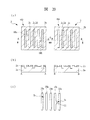
次に、本実施の形態1で用いた上記マスク2の一例を図6〜図8によって説明する。図6(a)はマスク2の全体平面図、図6(b)および(c)は、それぞれ図6(a)のA−A線およびB−B線の断面図である。図7および図8は図6のマスクの要部拡大断面図の一例である。なお、図6(a)は平面図であるが、図面を見易くするためハッチングを付した。
Next, an example of the
ここには、1枚のマスク2の主面(同一面)に、例えば2つの転写領域4A,4Bが配置されている場合が例示されている。各々の転写領域4A,4Bは、例えば平面長方形状に形成されており、各々の長辺が平行になるように所定の距離を隔てて配置されている。各転写領域4A,4Bは、例えば1個の半導体チップ(上記チップ形成領域)を転写する領域に相当する。なお、1枚のマスク2に配置される転写領域の数は、上記に限定されるものではなく種々変更可能である。
Here, a case where, for example, two
このマスク2を構成するマスク基板2aは、例えば平面四角形状の透明な合成石英ガラスからなり、その主面上の各々の転写領域4A,4Bには、マスクパターンが形成されている。このマスクパターンは、所定の集積回路パターンを転写するためのパターンであって、例えばクロム、酸化クロムまたはこれらの積層膜からなる遮光パターン2bと、マスク基板2aが部分的に露出されてなる光透過パターン2cとで構成されている。さらに、各々の転写領域4A,4B内において互いに隣接する光透過パターン2cのいずれか一方には上記溝シフタ2dが配置されている。本実施の形態1においては、上記転写領域4A,4Bの各々のマスクパターンの形状および寸法が同一となっている。ただし、転写領域4A,4Bは、各々の溝シフタ2dの配置が互いに逆になっている。すなわち、転写領域4A,4Bをウエハの1つの領域(チップ形成領域)に重ねて露光する際に、転写領域4Aの所定の光透過パターン2cを透過した光と、その転写領域4Aの所定の光透過パターン2cと平面的に重なる転写領域4Bの所定の光透過パターン2cを透過した光とでは、透過光の位相が180度反転するように溝シフタ2dが配置されている。
A
溝シフタ2dの深さZは、透過光の位相を180度反転させるために、Z=λ/(2(n−1))を満たすように形成されている。ただし、nは所定の露光波長の露光光に対する基板の屈折率、λは露光波長である。上記の例では、例えば露光波長248nmのKrFを用いているので、深さZは、例えば245nm程度である。上記のような多重露光処理を行わない場合、溝シフタ2dの深さの誤差の範囲は、例えば±3nm(位相角度で2度)程度であり極めて狭い。したがって、マスク2の製造が非常に難しく、マスク2の歩留まり低下の原因になっている。これに対して、本実施の形態1においては、溝シフタ2dの深さの誤差の範囲を、例えば±4nm〜8nm(位相角度で3度〜6度)程度に緩和できる。したがって、マスク2の製造上の容易性を大幅に向上させることが可能となっている。また、マスク2の製造歩留まりを大幅に向上させることが可能となっている。これについては後ほど詳細に説明する。
The depth Z of the
なお、上記転写領域4A,4B内には、実質的に集積回路を構成するパターンの他、例えば重ね合わせに用いるマークパターン、重ね合わせ検査に用いるマークパターンまたは電気的特性を検査する際に用いるマークパターン等のような実質的に集積回路を構成しないパターンも含まれている。また、転写領域4A,4Bの外周の遮光領域には、マスク基板2aの一部が露出されて、マスクアライメントマークや計測用マーク等のような他の光透過パターン2eが形成されている。
In addition, in the
図7および図8は、図6のマスク2の一対の光透過パターン2c,2c(互いに隣接する光透過パターン2c,2cであって、そのいずれか一方に溝シフタ2dが配置された光透過パターン対)部分の拡大断面図の一例を示している。
7 and FIG. 8 show a pair of
図7(a)〜(c)は、溝シフタ2dが上記基板溝シフタの場合を示している。すなわち、溝シフタ2dは、マスク基板2自体の表面に断面凹状の溝を掘ることで形成されている。図7(a)は、庇構造が無い場合を示している。すなわち、溝シフタ2dの側壁面と、遮光パターン2bの開口部(光透過パターン2c)の側壁面とがほぼ一致しており、その遮光パターン2bの開口部側端部に庇が形成されていない場合を示している。この場合の溝シフタ2dの深さZは、マスク2のパターン形成平坦面の高さを基準としてそこから溝シフタ2dの底の平坦面までの長さである。本実施の形態1においては、庇構造の無い図7(a)に示すマスク2であっても多重露光処理を行うことにより、ウエハ上に転写されるパターンの寸法精度を向上させることが可能となっている。
7A to 7C show a case where the
図7(b),(c)は、溝シフタ2dが上記微細庇型溝シフタの場合を示している。すなわち、溝シフタ2dの周辺(幅の狭い断面方向)においてマスク基板2aが溝シフタ2dの幅方向にオーバハングされ、その結果、溝シフタ2dに面した遮光パターン2bの端部が庇状に突き出た構造となっている。ここでは、例えばその遮光パターン2bの突き出た部分の庇長さPは、単色露光光の波長λを基準とした場合に、40%(P/λ=40%)以下である。ただし、本発明自体は、庇長さが70%以下のもの(例えば露光光の波長が248nmであれば、庇長さが150nm程度となるようなもの)にも適用できる。このような庇構造とすることにより、光の導波管現象を抑制することができる。すなわち、透過光の光強度が溝シフタ2dの側壁からの影響により減衰するのを抑制できる。したがって、本実施の形態1においては、多重露光処理に際して図7(b),(c)のマスク2を用いることにより、ウエハ上に転写されるパターンの寸法精度をさらに向上させることが可能となる。
FIGS. 7B and 7C show the case where the
図7(b)においては、溝シフタ2dが配置されない光透過パターン2cにおいても、マスク基板2aが掘り込まれ溝2fが形成されているが、溝シフタ2dが配置された光透過パターン2cと、溝2fが配置された光透過パターン2cとを透過した各々の光には180度の位相差が生じるようになっている。溝2fにおいても庇構造となっている。この溝シフタ2dを形成する際に、溝を形成する必要の無い光透過パターン2cをフォトレジスト膜で覆うと、フォトレジスト膜の塗布やパターニングの工程が増えることになる。そこで、図7(b)のマスク2においては、溝シフタ2dに庇構造を形成する際にフォトレジスト膜を形成せず、遮光パターン2bをエッチングマスクとしてマスク基板2aの表面(パターン形成面)をウエットエッチングする。溝2fは、その際に形成されたものである。この方法によれば、フォトレジスト膜の塗布やパターニング工程を無くせるので、マスク2の製造工程の簡略化が可能となる。このマスク2の場合の溝シフタ2dの深さZは、溝2fの底のマスク2のパターン形成平坦面の高さを基準としてそこから溝シフタ2dの底の平坦面までの長さである。また、図7(c)においては、図7(b)の溝2fが形成されていない場合が示されている。この場合の溝シフタ2dの深さは、図7(a)の場合と同じである。これら図7(a)〜(c)のマスク2の製造方法については後ほど詳細に説明する。
In FIG. 7B, even in the
また、図8(a)〜(c)は、溝シフタ2dが上記基板上薄膜溝シフタの場合を示している。すなわち、マスク基板2aの表面上にはシフタ膜2gが形成され、さらにその上に遮光パターン2bが形成された構造となっている。シフタ膜2gは、位相シフタとして作用する目的に適合した厚さ(=上記Zの式)で形成されており、例えばマスク基板2aと同等または同程度の光透過率および屈折率のSOG(Spin On Glass)等からなる。溝シフタ2dは、所定の光透過パターン2cのシフタ膜2gをマスク基板2aの表面が露出されるまで除去することで形成されている。この場合、溝シフタ2dの形成に際して、マスク基板2aとシフタ膜2gとのエッチング選択比を高くし、シフタ膜2gのエッチング速度の方がマスク基板2aのエッチング速度よりも速くなるようにする。すなわち、マスク
基板2aをエッチングストッパとして溝シフタ2dを形成する。これにより、溝シフタ2dの深さ(すなわち、シフタ膜2gの厚さ)および溝シフタ2dの底面の平坦性を極めて高い精度で形成できる。このため、透過光の位相誤差を大幅に低減または無くすことができるので、ウエハ上に転写されるパターンの寸法精度を大幅に向上させることが可能となる。なお、図8(a)〜(c)は、それぞれ図7(a)〜(c)に対応している。すなわち、図8(a)は庇構造の無い構造、図8(b)は庇および溝2fが形成された構造、図8(c)は庇のみで溝2fの無い構造である。
8A to 8C show the case where the
次に、本実施の形態1の多重露光方法の一例を図9によって説明する。図9には、ウエハ3の全体平面図であって、マスク2(図6参照)およびスキャナ1(図1参照)を用いて、ウエハ3の主面(フォトレジスト膜が塗布されている)に、所定の集積回路パターンを転写するためのステップアンドスキャン露光処理が例示されている。
Next, an example of the multiple exposure method of the first embodiment will be described with reference to FIG. FIG. 9 is an overall plan view of the
露光条件は、上記露光装置1の説明の際に説明したのと同じである。ウエハ3の主面上には、例えば厚さが200nm程度の絶縁膜(酸化シリコン膜等)が形成されている。また、その絶縁膜の上には、例えば厚さ500nm程度のポジ型のフォトレジスト膜が堆積されている。このフォトレジスト膜への露光量は、例えば25mJ/cm2とし、2重露光により、例えば50mJ/cm2となるように調整した。マスク2内の最小パターンは、ウエハ3上換算で、例えば150nmのライン・アンド・スペースである。
The exposure conditions are the same as those described in the description of the
まず、マスク2の転写領域4A,4Bを上記スキャニング露光処理によってウエハ3上の領域5Aに転写する。すなわち、マスク2とウエハ3とを各々の主面を平行に保ちながら相対的に逆方向(図9の上下縦方向)に移動させてウエハ3の主面上に上記スリット状の露光領域を移動させることにより、マスク2の転写領域4A,4B内のマスクパターン(集積回路パターン)を、ウエハ3の主面上の領域5Aに転写する。ウエハ3上における領域5Aの転写領域5A1,5A2は、それぞれマスク2の転写領域4A,4Bが転写された領域であり、ここではチップ形成領域に相当する。
First, the
続いて、ウエハ3を図9の右方向に水平移動し、領域5B,5Cを、上記と同様に順次露光する。これら領域5A,5B,5Cでの露光量は、必要量の1/2程度とする。なお、各領域5B,5C内の転写領域5B1,5C1は転写領域5A1と同じであり、転写領域5B2,5C2は転写領域5A2と同じである。
Subsequently, the
続いて、例えば転写領域5A1,5A2の一個分だけウエハ3を図9の上方向に移動させた後、領域5Dを上記と同様に露光する。この際、本実施の形態1においては、領域5D内の転写領域5D1と、先に転写した領域5C内の転写領域5C2とが平面的に重なるようにする。すなわち、マスク2における転写領域4Bが転写された転写領域5C2に、同じマスク2における転写領域4Aを平面的に重ねて転写する。なお、上述のようにマスク2の転写領域4A,4Bの同じ平面位置を透過した各々の光は、その位相が180度反転している。
Subsequently, for example, after the
続いて、ウエハ3を図9の左方向に水平移動し、領域5Eを、上記と同様に順次露光する。ここでは、領域5E内の転写領域5E1と、先に転写した領域5B内の転写領域5B2とが平面的に重なるようにする。すなわち、マスク2における転写領域4Bが転写された転写領域5C2に、同じマスク2における転写領域4Aを平面的に重ねて転写する。なお、ここでも、上述のようにマスク2の転写領域4A,4Bの同じ平面位置を透過した各々の光は、その位相が180度反転している。
Subsequently, the
これら領域5D,5Eでの露光量は、必要量の1/2程度とする。したがって、領域5A〜5Eが重なったところ(転写領域5B2,5E1および転写領域5C2,5D1等)では露光量が必要量となる。なお、各領域5D,5E内の転写領域5D1,5E1は転写領域5A1と同じであり、転写領域5D2,5E2は転写領域5A2と同じである。
The exposure amount in these
このような多重露光処理動作をウエハ3の全面内において繰り返すことにより、ウエハ3上に複数のチップ形成領域の集積回路パターンを転写する。ここでは、マスク2の転写領域4Aと転写領域4Bとが重なるようにする。すなわち、マスクパターンは同一であるが、透過光の位相が互いに反転するように溝シフタ2dを配置した転写領域4A,4Bを重ねて露光する。このような露光処理により、ウエハ3上に転写されるパターンの寸法精度を向上させることが可能となる。
By repeating such multiple exposure processing operation on the entire surface of the
また、上記の説明では、最外周の転写領域5A,5B,5Cの転写領域5A1,5B1,5C1が2重露光されていないが、この部分については、例えばマスク2の転写領域4Aをマスキングブレードにより遮光し、かつ、マスク2の転写領域4Bの転写領域が、図9のウエハ3の転写領域5A1に平面的に重なるように転写することにより2重露光を行った。転写領域5B1,5C1についても同様である。
In the above description, the transfer areas 5A1, 5B1, and 5C1 of the
次に、本実施の形態1の多重露光処理の作用を、発明者らが本発明をするのに検討した技術の問題点を交えながら説明する。 Next, the operation of the multiple exposure processing according to the first embodiment will be described with the problems of the technique studied by the inventors for carrying out the present invention.
まず、本発明者らが検討した技術の問題点を図10によって説明する。図10(a)は、位相シフトマスク50の断面形状を示している。位相シフトマスク50は、マスク基板50aと、その主面上に形成された遮光パターン50bと、光透過パターン50cとを有している。遮光パターン50bは、例えばクロム等からなる。互いに隣接する光透過パターン50c,50cの一方には、その各々の透過した光に180度の位相差を与えるため、マスク基板50aを所定の深さに掘り込み溝シフタ50dを形成している。ここでは、基板溝シフタであって、微細庇型溝シフタでない場合を例示している。また、互いに隣接する光透過パターン50c,50cの平面の形状および寸法は同じである。
First, the problem of the technique examined by the present inventors will be described with reference to FIG. FIG. 10A shows the cross-sectional shape of the
この位相シフトマスク50を用いて投影露光すると、被投影基板上で得られる光強度は、図10(b)に示すように、溝シフタ50dが配置された光透過パターン50cを透過した光の強度51aは、溝シフタ50dが配置されていない光透過パターン50cを透過した光の強度51bに比べて小さくなってしまう。これはマスク基板50aを掘り込んだ溝シフタ5dの側壁の影響により透過光の強度が減衰するためである。したがって、通常の方法(1回露光)によりフォトレジスト膜にパターンを転写すると、図10(c)の露光平面に示すように、溝シフタ50dの配置された光透過パターン50cが転写されたフォトレジストパターン52aの幅方向の寸法w50の方が、溝シフタ50dの配置されていない光透過パターン50cが転写されたフォトレジストパターン52bの幅方向の寸法w51よりも小さくなってしまう。すなわち、本来同じ平面寸法で転写されるべきフォトレジストパターン52a、52bの平面寸法が溝シフタ50dの有無によって異なってしまう。
When projection exposure is performed using this
これを防止するため、図11(a)に示すように、溝シフタ50dを上記微細庇型溝シフタ構造とすることが採用されている。すなわち、マスク基板50aの溝シフタ50dの側壁が遮光パターン50bの下に隠れるように調整し、遮光パターン50bの端部が庇長さPだけ庇状に張り出す構造となっている。この構造にすることによって、図11(b)に示すように、溝シフタ50dが配置された光透過パターン50cを透過した光の強度53aは、溝シフタ50dが配置されていない光透過パターン50cを透過した光の強度53bとほぼ同じとなるが、完全には等しくならないのが現状である。したがって、図11(c)の露光平面に示すように、溝シフタ50dの配置された光透過パターン50cが転写されたフォトレジストパターン55aの幅方向の寸法w52と、溝シフタ50dの配置されていない光透過パターン50cが転写されたフォトレジストパターン55bの幅方向の寸法w53とはほぼ等しくなるが、やはり完全には等しくならない。
In order to prevent this, as shown in FIG. 11A, it is adopted that the
ここで、本発明者らは、さらに詳しく調査・研究した。図12は、その調査・研究結果を示している。横軸はラインアンドスペース(パターン)の寸法を示し、縦軸は各寸法におけるフォトレジストパターン55a,55bの寸法差(w52−w53)を示している。ここでのパターン転写の条件は、例えば次の通りである。すなわち、庇長さPは、例えば100nmとし、解像パターンの寸法は、例えば0.12〜0.18μmまで変化させた。露光条件は、上記露光装置1の説明の際に説明したのと同じである。この結果、ウエハ上に形成しようとしているパターンの寸法の値に応じて、フォトレジストパターン55a,55bの寸法w52,w53の差が異なることが明らかになった。したがって、ただ単純に溝シフタを庇構造としただけでは、ウエハ上に転写されるパターンの寸法差を無くすことが困難であることが判明した。
Here, the present inventors investigated and studied in more detail. FIG. 12 shows the results of the survey and research. The horizontal axis indicates the dimension of the line and space (pattern), and the vertical axis indicates the dimension difference (w52−w53) between the
そこで、本実施の形態1においては、上記のようにマスク2のマスクパターンを多重露光処理によってウエハ3に転写する。この際、多重露光するマスクパターンの溝シフタ2dの配置が互いに反転するようにして行う。これにより、ウエハ3上に転写されるパターンにおいて、位相の絶対値誤差による転写パターンの寸法差、溝シフタ2dの有無による転写パターンの寸法差、ウエハ上に形成しようとしているパターンの寸法の違いによる転写パターンの寸法差を低減または無くすことができるので、転写パターンの寸法精度を向上させることができ、また、転写パターンの寸法を均一化することが可能となる。
Therefore, in the first embodiment, the mask pattern of the
上記した本実施の形態1の多重露光の効果をシミュレーションにより調べた結果を図13に示す。また、比較のため1回露光の結果を図14に示す。いずれもウエハ上で得られる光強度分布を示している。また、いずれの露光処理においても通常の溝シフタ(微細庇型溝シフタでない)構造の位相シフトマスクを用いた。 FIG. 13 shows the result of examining the effect of the multiple exposure of the first embodiment described above by simulation. For comparison, the result of single exposure is shown in FIG. Both show the light intensity distribution obtained on the wafer. In any of the exposure processes, a phase shift mask having a normal groove shifter (not a fine saddle groove shifter) structure was used.
図13に示すように、本実施の形態1によれば、溝シフタ2dが互いに反転されるように配置された転写領域4A,4Bを2重露光しているため、互いに隣り合った光強度ピーク6a,6bで均一な光強度が得られていることが分かる。これに対して1回露光の場合、図14に示すように、溝シフタが配置された光透過パターンを透過した光の強度56aの方が、溝シフタの無い光透過パターンを透過した光の強度56bよりも小さいことが分かる。
As shown in FIG. 13, according to the first embodiment, since the
図15は、本実施の形態1の多重露光処理の作用を簡略化して模式的に示している。図15(a)はマスク2の重ね合わせる2つの転写領域4C,4Dを示し、同図(b)は(a)のA−A線およびB−B線の断面図を示している。転写領域4C,4Dの各々には、互いに隣接する帯状の光透過パターン2c,2cが形成されている。転写領域4C,4Dの光透過パターン2c,2cの平面形状および寸法は同じである。転写領域4C,4Dのいずれにおいても互いに隣接する光透過パターン2c,2cの一方に溝シフタ2dが配置されているが、その配置が転写領域4Cと転写領域4Dとを重ね合わせた時に反対となるように、すなわち、透過光の位相が180度反転するようになっている。図15(c)は、各々の転写領域4C,4Dを透過した光の強度分布を示している。転写領域4C,4Dの各々を透過した光の強度分布では、いずれも溝シフタ2dが配置された光透過パターン2cを透過した光の強度が減衰している。これに対して、図15(d)は、転写領域4C,4Dを重ねて露光した場合の透過光の強度分布を示している。この場合は、溝シフタ2dの配置された光透過パターン2cを透過した光と、溝シフタ2dの無い光透過パターン2cを透過した光とが同一箇所に重ねて露光されることにより、双方の光強度を平均化することができ、光強度のアンバランスをキャンセルすることができるので、光強度分布の均一化を図ることが可能となる。
FIG. 15 schematically shows a simplified operation of the multiple exposure process of the first embodiment. FIG. 15A shows two
したがって、本実施の形態1の多重露光処理によれば、位相の絶対値精度(誤差精度)が多少悪くても、180度位相差の時と同じ解像特性を得ることが可能となる。すなわち、位相の誤差の許容量(位相の絶対値精度)を、例えば3度〜6度(溝シフタ2dの深さで±4nm〜±8nm)程度に緩和できる。したがって、マスク2の製造上の容易性を大幅に向上させることが可能となる。また、マスク2の製造歩留まりを大幅に向上させることが可能となる。特に、重ね合わせる転写領域4A,4Bを同一マスク2の同一平面内の異なる平面位置に形成する本実施の形態1においては、その重ね合わせる転写領域を別々のマスクに形成する場合に比べて、溝シフタ2dの深さおよびその誤差量をマスク2の面内においてほぼ均一にすることができるので、その重ね合わせる転写領域を別々のマスクに形成する場合よりも相対的に高い位相の絶対値精度を確保しつつ、容易にマスク2を製造することが可能となる。
Therefore, according to the multiple exposure processing of the first embodiment, even if the absolute value accuracy (error accuracy) of the phase is somewhat poor, it is possible to obtain the same resolution characteristics as when the phase difference is 180 degrees. That is, the allowable amount of phase error (the absolute value accuracy of the phase) can be relaxed to, for example, about 3 degrees to 6 degrees (± 4 nm to ± 8 nm as the depth of the
また、本実施の形態1の多重露光処理によれば、溝シフタ2の有無によって隣接する転写パターンの寸法が変動するのを抑制または防止することが可能となる。このため、転写されるパターンの寸法精度を大幅に向上させることが可能となる。また、溝シフタ2の有無による隣接転写パターンの寸法変動を低減または防止できるので、微細庇型溝シフタ構造とする必要性が無くなる。このため、マスク2の製造上の容易性を大幅に向上させることが可能となる。庇構造は、庇長さが長いほど効果があるが、ウエハ上のパターンの微細化要求に伴いマスク2上の遮光パターン2bも微細化されているので、庇長さの増長には限界がある。本実施の形態1の技術は、庇構造を採らなくてもパターン寸法精度の向上を図れるので、パターンの微細化に適した技術である。
In addition, according to the multiple exposure process of the first embodiment, it is possible to suppress or prevent the adjacent transfer pattern from fluctuating depending on the presence or absence of the
さらに、本実施の形態1の多重露光処理によれば、ウエハ3上に転写しようとしているパターンの寸法に応じて隣接パターンの寸法差が変動するのを抑制または防止することが可能となる。したがって、ウエハ3に転写されたパターンの寸法精度を転写領域内全体において向上させることが可能となる。
Furthermore, according to the multiple exposure process of the first embodiment, it is possible to suppress or prevent the dimensional difference between adjacent patterns from fluctuating according to the dimension of the pattern to be transferred onto the
実際にパターンを転写した結果、例えば150nmのパターンがチップ全面で150nm±10nmの精度で良好に形成できた。また、隣り合うパターンの解像寸法に特別な傾向は見られなかった。マスク2の欠陥によるパターンのショート等の発生も認められなかった。一方、同一条件で、2重露光を行わない技術では150nmのパターンがチップ全面で150nm±22nmの精度で形成された。また、溝シフタを配置したパターンと配置していないパターンの解像寸法差は8nmで、溝シフタを配置した方が細く形成された。
As a result of actually transferring the pattern, for example, a 150 nm pattern was successfully formed with an accuracy of 150 nm ± 10 nm on the entire surface of the chip. In addition, no special tendency was observed in the resolution dimension of adjacent patterns. The occurrence of a pattern short circuit due to a defect in the
次に、本発明者らが検討した他の問題点について説明する。すなわち、投影光学系を用いたパターンの転写では、投影レンズの種々の収差によって投影像に歪みが発生する。この現象は、投影面の位置によって異なる。代表的な収差として、例えば転写像の歪曲がある。これは、投影パターンの位置ずれであり、例えば絶対格子に配置されたパターンが糸巻き状や樽状等に歪んで転写される。すなわち、通常は、投影レンズに種々の収差があるため、設計通りのパターンの形成が困難である。 Next, other problems studied by the present inventors will be described. That is, in pattern transfer using a projection optical system, a projection image is distorted by various aberrations of the projection lens. This phenomenon varies depending on the position of the projection plane. A typical aberration is, for example, distortion of a transferred image. This is a misalignment of the projection pattern. For example, a pattern arranged in an absolute lattice is distorted and transferred in a pincushion shape or a barrel shape. That is, normally, since the projection lens has various aberrations, it is difficult to form a pattern as designed.
ここで、ステッパを用いたパターンの転写では、1ショットで複数の集積回路パターンを転写し、ずらし露光によって多重露光を行うと、パターンの位置歪みの影響で重ね誤差が生じ、解像特性が大幅に劣化し、実用は困難である。図16は、その様子を模式的に示している。ここでは、ステッパでのパターンの転写を例にとって説明する。符号の60は、理想格子上の設計パターンであり、歪みの無い四角形状のパターンとなっている。また、符号の61,62が実際に転写された転写パターンである。転写パターン61は理想格子に対して糸巻き状に位置ずれして転写され、転写パターン62は理想格子に対して樽状に位置ずれして転写されている。このように、投影レンズの収差は、パターンの位置ずれを引き起こし、転写位置によってその挙動が異なる。
Here, in pattern transfer using a stepper, if multiple integrated circuit patterns are transferred in one shot and multiple exposure is performed by shift exposure, an overlay error occurs due to the effect of pattern position distortion, and resolution characteristics are greatly improved. It is difficult to put it to practical use. FIG. 16 schematically shows such a state. Here, a description will be given taking a pattern transfer with a stepper as an example.
また、図17(a)、(b)はマスク上の異なる平面位置座標の転写領域をステッパを用いて転写した様子を模式的に示している。図17(a),(b)の符号63a,63bは、上記マスク上の異なる平面位置の同一パターンで構成される転写領域を実際に転写した際の転写領域の全体的な位置ずれの状態を模式的に示したものである。図17(a)に示すように、転写領域63a,63bは、互いに異なった形状で形成(転写)されるため、図17(b)に示すように、両者を重ねた場合、パターンの位置ずれが生じるので、良好なパターンの形成(転写)が困難である。
FIGS. 17A and 17B schematically show a state in which transfer regions of different plane position coordinates on the mask are transferred using a stepper.
そこで、本実施の形態1においては、上記のように、マスク2のマスクパターンをスキャナを用いてウエハ3上に転写する際に、マスク2の同一パターンをウエハ3の同一領域に多重露光する。スキャナを用いた露光処理においては、マスク2上のパターンをスリットを介してウエハ3上に転写する。この場合、スキャン方向においては収差分布が均一となる。すなわち、スキャン方向に重ね露光を行っても、収差起因の重ね誤差は生じない。したがって、重ね露光が可能となる。
Therefore, in the first embodiment, as described above, when the mask pattern of the
スキャナを用いた場合のパターンの転写状態を図18に示す。符号の7は、理想格子上の設計パターンであり、歪みの無い四角形状のパターンとなっている。符号の7aは設計パターン7においてスキャン方向(図18の上下縦方向)に平行な辺を示し、符号の7bは設計パターン1においてスキャン方向に直交する辺を示している。なお、ここで、スキャン方向は、投影レンズの走査方向であり、ウエハ3等の被露光処理基板はこれと反対の方向に移動するようになっている。符号の8は、実際に転写された転写パターンを示している。符号の8aは転写パターン8においてスキャン方向に平行な辺を示し、符号の8bは転写パターン8においてスキャン方向に直交する辺を示している。また、符号9a,9bは、上記マスク2上の異なる平面位置の同一パターンで構成される転写領域4A,4Bが実際に転写された転写領域の全体的な状態を模式的に示している。
FIG. 18 shows a pattern transfer state when a scanner is used.
スキャナを用いた露光処理においては、スキャン方向に直交する方向(図18の左右横方向)においてレンズ収差に起因する位置ずれが生じるが、スキャン方向においてレンズ収差が同一となるため同じ形状が保たれる。例えば転写パターン8においてスキャン方向に平行な辺8aは設計パターン7においてスキャン方向に平行な辺7aに対して位置ずれが見えるが、そのずれ量はスキャン方向に同一である。また、転写パターン8においてスキャン方向に直交する辺8bは、設計パターン7においてスキャン方向に直交する辺7bとほぼ重なっており、位置ずれが見られない。すなわち、スキャナを用いた露光処理においては、転写領域9a,9bのパターンは、スキャン方向に直交する方向においてほぼ同じ変形を持つようになり、しかもスキャン方向においてほぼ同じ形状で形成される。したがって、転写領域9a,9bをウエハ3等の被露光処理基板上の同一の領域に2重露光しても、高い重ね合わせ精度で形成することができる。本発明は、この特性を利用している。
In the exposure processing using a scanner, a positional shift caused by lens aberration occurs in a direction orthogonal to the scan direction (the horizontal direction in FIG. 18), but the same shape is maintained because the lens aberration is the same in the scan direction. It is. For example, the side 8a parallel to the scanning direction in the transfer pattern 8 can be misaligned with respect to the side 7a parallel to the scanning direction in the
次に、本発明者らが検討したさらに他の問題点について説明する。図19の(a)は溝シフタ2dが形成されたマスク64の要部平面図、(b)は(a)のA−A線の断面図を示している。
Next, still another problem studied by the present inventors will be described. FIG. 19A is a plan view of an essential part of the
転写領域65には、例えば150nmのラインアンドスペースを配置した。互いに隣接する光透過パターン66の一方に溝シフタ67が配置されている。この転写領域65に欠陥68a,68bが存在している。欠陥68bの平面寸法は欠陥68aのそれよりも相対的に大きい。
In the
このような転写領域65を、2重露光処理を行わないで(すなわち、1回露光)スキャニング露光した結果を図19(c)に示す。この場合、正常なフォトレジストパターン69の他に、マスク64の欠陥68a,68bに起因するフォトレジスト残り70a,70bが転写されていた。このうち、フォトレジスト残り70bはパターン間のショート不良の原因となっていた。なお、図19(c)の破線は、フォトレジストパターン69およびフォトレジスト残り70bと、マスク64の光透過パターン66および欠陥68a,68bとの相対的な位置関係が分かるように、光透過パターン66および欠陥68a,68bを示したものである。
FIG. 19C shows the result of scanning exposure of such a
これに対して、本実施の形態1による上記2重露光方法では、図20に示す結果が得られた。図20(a)は、同一マスク2の同一平面の異なる平面位置に形成された転写領域4A1,4B2の平面図、(b)は(a)のA−A線およびB−B線の断面図を示している。転写領域4A1,4B1には、互いに同一マスクパターンが配置されているが、溝シフタ2dの配置が上記のように反対(位相が180度反転)になっている。転写領域4A1には上記欠陥68a,68bが存在している。ラインアンドスペースの寸法は、図19のマスクと同じである。ところで、本実施の形態1の露光処理においては、上記のような転写領域4A1,4B1をそれぞれ1/2の露光量で重ね露光するので、欠陥部分と欠陥の存在しない部分とが多重露光されることになる。その結果、マスク2の欠陥の転写を低
減または完全に無くすことが可能となる。その転写結果を図20(c)に示す。
In contrast, in the double exposure method according to the first embodiment, the result shown in FIG. 20 was obtained. 20A is a plan view of transfer regions 4A1 and 4B2 formed at different planar positions on the same plane of the
マスク2の転写領域4A1内の欠陥68aに対応する位置S1においては、フォトレジストパターン10aの変形が確認されなかった。一方、マスク2の転写領域4A1内の欠陥68bに対応する位置S2では、フォトレジストパターン10aの変形(フォトレジスト残り11)が認められたが、パターン間のショート不良には至ってないことが分かった。このようなパターン欠陥は検査の結果、必要ならば、FIB(Focused Ion Beam)等のようなエネルギービームを用いた修正処理によって修正することも可能である。この場合、パターン変形量を比較的小さくすることができるので、その修正を容易にすることが可能である。なお、図20(c)の破線は、フォトレジストパターン10aおよびレジスト残り11と、フォトマスク4A1の光透過パターン2cおよび欠陥68a,68bとの相対的な位置関係が分かるように、その光透過パターン2cおよび欠陥68a,68bを示している。
In the position S1 corresponding to the
このように本実施の形態1の多重露光処理によれば、マスク2の転写領域にランダムに存在する欠陥を平均化または除去することができるので、マスク2の欠陥の転写を抑制または防止できる。また、欠陥が転写されたとしても、その欠陥の転写限界を拡大することができる。例えばステッパでは、フォトマスク上の0.2μm以上の欠陥が転写されたが、本実施の形態1では、フォトマスク4上の0.4μm以上のより大きな欠陥が転写される。すなわち、マスク2上において0.4μm未満の欠陥は無視することができるので、欠陥検査の寸法限界を緩和することができる。すなわち、マスク2の欠陥検査および欠陥修正を容易にすることが可能となる。したがって、マスク2の製造上の容易性を向上させることが可能となる。
As described above, according to the multiple exposure processing of the first embodiment, it is possible to average or remove defects randomly present in the transfer region of the
さらに、本発明者らは、本実施の形態1の露光処理における多重露光の回数を増やした場合について、マスク2上の欠陥が転写パターンの寸法に与える影響を調査した。この場合の露光条件は、上記露光装置1の説明の際に説明したのと同じである。図21には、この際に用いたマスク2の転写領域4A2,4B2の要部平面図が示されている。図21(a)は欠陥が存在する転写領域4A2の要部平面図を示し、図21(b)は欠陥が存在しない転写領域4B2の要部平面図を示している。図21(a),(b)の転写領域4A2,4B2には、互いの長辺が平行になるように並んで配置された平面長方形状の複数の光透過パターン2c1,2c2がそれぞれ配置されている。光透過パターン2c1,2c2の幅bおよび隣接間のスペース寸法cは、例えば0.25μm程度である。ただし、図21(a)には、例えば次の3種類の欠陥が示されている。すなわち、例えば一辺の寸法が上記スペース寸法よりも小さい寸法の平面正方形状の透明欠陥68c、長辺の寸法が上記スペース寸法と等しい平面長方形状の透明欠陥68dおよび一辺の寸法が上記幅よりも小さい寸法の平面正方形状の遮光欠陥68eである。欠陥の大きさは変数aで示した。露光処理においては、欠陥が存在する図21(a)のパターンと、欠陥が存在しない図21(b)のパターンとを複数回重ね露光した。そして、光透過パターン2c1,2c2の寸法b1〜b3に対する転写パターンの寸法を評価した。その評価結果を図22に示す。
Further, the inventors investigated the influence of defects on the
図22(a)〜(c)は、それぞれ寸法b1〜b3の測定結果を示している。図22(a)〜(c)において、1重は図21(a)の欠陥のある転写領域4A2のみで露光した場合、2重は図21(a)の欠陥のある転写領域4A2と図21(b)の欠陥の無い転写領域4B2とを重ね露光した場合、3重は上記2重露光にさらに図21(b)の欠陥の無い転写領域4B2を重ね露光した場合、4重は上記3重露光にさらに図21(b)の欠陥の無い転写領域4B2を重ね露光した場合をそれぞれ示している。いずれの欠陥においても、無欠陥パターンの重ね回数を増やすほど欠陥の影響が少なくなることが分かる。また、ここではパターンの寸法に着目して評価した場合について説明したが、パターンの断線、ショート等の評価をした結果、3重露光以上では、欠陥の大きさによらず、断線、ショートの発生を防止できた。本実施の形態1では、位相シフトマスクを用いるので、位相反転が生じることを考慮すると重ね合わせ回数は偶数回が好ましい。 22A to 22C show the measurement results of the dimensions b1 to b3, respectively. 22A to 22C, when the single exposure is performed only in the defective transfer area 4A2 in FIG. 21A, the double is the same as the defective transfer area 4A2 in FIG. When the transfer area 4B2 having no defect of (b) is overlaid and exposed, the triple is exposed to the above double exposure and the transfer area 4B2 of FIG. FIG. 21B shows a case where the transfer area 4B2 having no defect is further exposed for exposure. It can be seen that in any defect, the influence of the defect decreases as the number of times of overlapping the defect-free pattern increases. In addition, although the case where the evaluation was made by paying attention to the dimension of the pattern is described here, as a result of the evaluation of the pattern disconnection, the short-circuit, etc., the occurrence of the disconnection, the short-circuit occurs regardless of the size of the defect in the triple exposure or more. We were able to prevent. In the first embodiment, since the phase shift mask is used, the number of overlays is preferably an even number in consideration of the occurrence of phase inversion.
また、本実施の形態1の多重露光方法によれば、ウエハ上に転写されるパターンの寸法分布精度も向上させることができた。これを図23および図24によって説明する。図23は、2重露光処理を行わないでスキャナで露光(すなわち、1回露光)した結果を示している。位置S1〜S4が1個のチップ、位置S5〜S8が他の1個のチップである。寸法分布は、マスクの寸法分布の影響を受けてチップの中央部が細くパターン形成されており、最大寸法と最小寸法との差は、例えば0.063μm程度であった。これに対して本実施の形態1の多露光方法においては、図24に示すように、図23の位置S1〜S4と、位置S5〜S8を重ね露光するため、寸法の平均化がなされ、転写パターンの寸法分布精度を向上させることができた。ここでは、最大寸法と最小寸法との差を、例えば0.036μmであった。すなわち、寸法のばらつきを約半分に低減することができた。 Further, according to the multiple exposure method of the first embodiment, the dimensional distribution accuracy of the pattern transferred onto the wafer can be improved. This will be described with reference to FIGS. FIG. 23 shows the result of exposure with a scanner (ie, one exposure) without performing double exposure processing. The positions S1 to S4 are one chip, and the positions S5 to S8 are another chip. The dimensional distribution is affected by the dimensional distribution of the mask, and the central portion of the chip is thinly formed. The difference between the maximum dimension and the minimum dimension is, for example, about 0.063 μm. On the other hand, in the multiple exposure method of the first embodiment, as shown in FIG. 24, the positions S1 to S4 and the positions S5 to S8 in FIG. The dimensional distribution accuracy of the pattern could be improved. Here, the difference between the maximum dimension and the minimum dimension was, for example, 0.036 μm. That is, the dimensional variation could be reduced to about half.
上記露光条件で多重露光処理を行った本実施の形態1においては、例えば0.25μmのパターンがチップの全面において0.25±0.02μmの精度で良好に形成できた。また、マスク2の欠陥によるパターン間のショート不良等の発生は認められなかった。
In the first embodiment in which multiple exposure processing is performed under the above exposure conditions, for example, a pattern of 0.25 μm can be satisfactorily formed with an accuracy of 0.25 ± 0.02 μm on the entire surface of the chip. In addition, the occurrence of short-circuit defects between patterns due to defects in the
次に、本実施の形態1のマスク2の製造方法を説明する。まず、本実施の形態1のマスク2の製造方法に先立って、本発明者らが検討したマスク製造上の問題点について説明する。
Next, the manufacturing method of the
図25は、本発明者らが検討したマスクの製造工程中の要部断面図を示している。この技術においては、まず、図25(a)に示すように、マスク基板80上に通常の方法で遮光パターン81および光透過パターン82を形成する。遮光パターン82は、クロム(Cr)等からなる。続いて、図25(b)に示すように、シフタ形成用のレジストパターン83をマスク基板80上に通常の方法で形成した後、レジストパターン83から露出するマスク基板80をドライエッチング処理によって掘り込み、位相シフタ形成用の溝84を形成する。ここで、位相差を180度に高精度に制御することが困難な場合は、レジストパターン83を図25(c)に示すように除去した後、位相差を測定し、次の目標エッチング量を決定する。その後、図25(d)に示すように、マスク基板80上に再度シフタ形成用のレジストパターン85を通常の方法で形成し、目標エッチング量でマスク基板80に対してウエットエッチング処理を施す。この際、ウエットエッチング等のような等方エッチングにより、遮光パターン81の下部も含めエッチングする。これにより、上記微細庇型の溝シフタ86を形成する。最後に、レジストパターン85を除去することにより、図25(e)に示すように、所望のマスクパターンおよび溝シフタ86を有するマスク構造が完成する。
FIG. 25 shows a cross-sectional view of the main part in the mask manufacturing process studied by the present inventors. In this technique, first, as shown in FIG. 25A, a
上記のように溝シフタを有するマスクにおいては、位相制御(すなわち、溝の深さ)に高い精度が要求されている。溝シフタの深さは、露光波長に依存しているので、パターンの微細化要求により露光波長も短くなっていることから浅くなる傾向にある。したがって、溝も掘り易いようにも思われるが、実際は、その溝に許される誤差範囲が溝の深さに対して決まり一定なので、溝シフタの深さ精度自体は厳しいままである。このため、マスクの製造が難しい。また、その高精度な位相制御や庇形状の形成を実現するために、マスクの製造工程が複雑化している。これらにより、マスクの製造工程数の増加や歩留まりの低下が大きな問題となっている。 As described above, in a mask having a groove shifter, high accuracy is required for phase control (that is, groove depth). Since the depth of the groove shifter depends on the exposure wavelength, it tends to become shallower because the exposure wavelength is shortened due to the demand for pattern miniaturization. Therefore, although it seems to be easy to dig a groove, in reality, the error range allowed for the groove is determined and constant with respect to the depth of the groove, so the depth accuracy of the groove shifter itself remains severe. For this reason, it is difficult to manufacture a mask. In addition, the mask manufacturing process is complicated in order to realize the highly accurate phase control and the formation of the ridge shape. As a result, an increase in the number of mask manufacturing processes and a decrease in yield are serious problems.
次に、本実施の形態1のマスク2の製造方法例を図26の工程に沿って図27および図28によって説明する。
Next, an example of a method for manufacturing the
まず、マスクパターン形成工程においては、図27(a)に示すように、マスク基板2aの主面上全面に、例えばクロム等からなる遮光膜をスパッタリング法等によって堆積する(工程201)。続いて、その遮光膜上に、フォトレジスト膜を塗布した後、これをパターニングすることで所定のフォトレジストパターンを形成する(工程202)。その後、そのフォトレジストパターンから露出する遮光膜部分をエッチング法等によって除去することにより、遮光パターン2bおよび光透過パターン2cを形成する(工程203)。続いて、フォトレジストパターンを除去した後(工程204)、パターンの欠け等の有無を検査する(工程205)。その後、その検査結果に基づいて修正できるものについて修正する(工程206)。ここまでの工程は、上記発明者らが検討したマスクの製造技術と同じである。
First, in the mask pattern forming step, as shown in FIG. 27A, a light shielding film made of, for example, chromium is deposited on the entire main surface of the
次いで、位相シフタ形成工程においては、マスク基板2a上の遮光パターン2bの形成面上に、フォトレジスト膜を塗布した後、そのフォトレジスト膜を図27(b)に示すようにパターニングすることにより、所定の光透過パターンが露出され、それ以外を覆うようなフォトレジストパターン12を形成する(工程207)。続いて、そのフォトレジストパターン11をエッチングマスクとして、そこから露出するマスク基板2aを異方性のドライエッチング法によってエッチングすることにより、溝シフタ2dを形成する(工程208)。その後、フォトレジストパターン12を図27(c)に示すように除去した後(工程209)、そのマスク2の透過光の位相を検査することにより(工程210)、マスク2を製造する。
Next, in the phase shifter forming step, a photoresist film is applied on the formation surface of the
このように本実施の形態1においては、上記のようにマスクの位相差の絶対値制御(誤差許容量)の精度を緩和することができるので、マスク2の製造プロセス途中に位相差の測定等を行う必要が無いため、溝シフタ形成用のフォトレジストパターンの形成工程を1回のみにすることができる。また、本実施の形態1においては、溝シフタの有無での光強度の差を多重露光によって打ち消すことができるので、遮光パターンに庇を形成する必要が無い。したがって、本実施の形態1においては、上記発明者検討技術に比べてマスク2の製造工程を簡略することができる。すなわち、マスク2の製造工程数を低減できるので、マスク2の製造時間を短縮することが可能となる。また、マスク2の歩留まりを向上させることが可能となる。
As described above, in the first embodiment, since the accuracy of the absolute value control (allowable error) of the phase difference of the mask can be relaxed as described above, the phase difference is measured during the manufacturing process of the
ところで、極端なシフタの有無により光強度の差が解像特性に悪影響を及ぼす場合は、図28に示すように、検査工程210の後、マスク2の表面全面に対して等方的なウエットエッチングを施すことが有効である。すなわち、溝シフタ2dおよび溝シフタ2dを配置していない部分の双方にウエットエッチングを施すことにより、庇構造を形成する(工程211a)。これは前記図7(b)に示した構造のマスク2の製造方法である。この場合、溝シフタ2dの有無での光強度の差を軽減することができ、解像特性の低下を防止できる。
If the difference in light intensity adversely affects the resolution characteristics due to the presence or absence of an extreme shifter, isotropic wet etching is performed on the entire surface of the
さらに、本実施の形態1においては、上記のように位相の絶対値制御精度を緩和できるので、溝形成工程208後に、その溝シフタ2dの加工時にマスクとして用いたフォトレジストパターン12(図27(b)参照)をマスクとしてマスク2に対して等法的なウエットエッチング処理を施すことにより、庇構造を形成しても良い(工程211b)。これは、前記図7(c)で示した構造のマスク2の製造方法である。構造的には上記本発明者らが検討した図25(e)と同じ構造となるが、本実施の形態1では、フォトレジスト膜の塗布およびパターニング工程を1回にできるので、上記検討技術よりもマスク2の製造工程の簡略化が可能である。
Further, in the first embodiment, since the absolute value control accuracy of the phase can be relaxed as described above, after the
次に、本発明の技術思想をDRAM(Dynamic Random Access Memory)の各パターンを露光処理によって転写する場合に適用した一例を図29および図30に示す。図30は図29のA−A線の断面図である。本実施の形態の露光方法をDRAMの製造技術に適用することにより、特に、チップ内の欠陥数を低減できるので、ビット救済チップ数を低減することが可能となる。 Next, FIG. 29 and FIG. 30 show an example in which the technical idea of the present invention is applied to the case where each pattern of a DRAM (Dynamic Random Access Memory) is transferred by exposure processing. 30 is a cross-sectional view taken along line AA of FIG. By applying the exposure method of the present embodiment to the DRAM manufacturing technique, in particular, the number of defects in the chip can be reduced, so that the number of bit relief chips can be reduced.
半導体基板3Sは、例えば平面略円形状の上記ウエハ3から切り出されたDRAMの平面四角形状のチップを構成する部分であり、例えばp型の単結晶シリコンからなる。この半導体基板3Sの主面にはp型ウエル21が形成され、そのp型ウエル21にDRAMのメモリセルが形成されている。なお、メモリセルが形成された領域(メモリアレイ)のp型ウエル21は、半導体基板3Sの他の領域に形成された入出力回路などからノイズが侵入するのを防ぐために、その下部に形成されたn型半導体領域22によって半導体基板3Sから電気的に分離されている。
The
メモリセルは、メモリセル選択用MISFETQsの上部に情報蓄積用容量素子Cを配置したスタックド構造で構成されている。メモリセル選択用MISFETQsはnチャネル型MISFETで構成され、p型ウエル21の活性領域Lに形成されている。活性領域Lは、図29のX方向に沿って真っ直ぐに延在する細長い島状のパターンで構成されており、それぞれの活性領域Lには、ソース、ドレインの一方(n型半導体領域)を互いに共有するメモリセル選択用MISFETQsがX方向に隣接して2個形成されている。
The memory cell has a stacked structure in which an information storage capacitive element C is arranged above the memory cell selection MISFETQs. The memory cell selection MISFET Qs is composed of an n-channel type MISFET and is formed in the active region L of the p-
活性領域Lを囲む素子分離領域は、p型ウエル21に開孔した浅い溝に酸化シリコン膜等からなる絶縁膜を埋め込んで形成した溝型の素子分離部(トレンチアイソレーション)23によって構成されている。この溝型の素子分離部23に埋め込まれた絶縁膜は、その表面が活性領域Lの表面とほぼ同じ高さになるように平坦化されている。このような溝型の素子分離部23によって構成された素子分離領域は、活性領域Lの端部にバーズビーク(bird's beak)ができないので、LOCOS(Local Oxidization of Silicon:選択酸化)法で形成された同一寸法の素子分離領域(フィールド酸化膜)に比べて活性領域Lの実効的な面積が大きくなる。
The element isolation region surrounding the active region L is constituted by a groove type element isolation portion (trench isolation) 23 formed by embedding an insulating film made of a silicon oxide film or the like in a shallow groove opened in the p-
メモリセル選択用MISFETQsは、主としてゲート絶縁膜24、ゲート電極25およびソース、ドレインを構成する一対のn型半導体領域26、26によって構成されている。ゲート電極25はワード線WLと一体に構成されており、同一の幅、同一のスペースでY方向に沿って直線的に延在している。ゲート電極25(ワード線WL)は、例えばP(リン)などのn型不純物がドープされた低抵抗多結晶シリコン膜と、その上部に形成されたWN(タングステンナイトライド)膜などからなるバリアメタル層と、その上部に形成されたW(タングステン)膜などの高融点金属膜とで構成されたポリメタル構造を有している。ポリメタル構造のゲート電極25(ワード線WL)は、多結晶シリコン膜やポリサイド膜で構成されたゲート電極に比べて電気抵抗が低いので、ワード線の信号遅延を低減することができる。ただし、ゲート電極25を、多結晶シリコン膜の単体膜で構成しても良いし、多結晶シリコン膜上にタングステンシリサイド等のようなシリサイド膜を積み重ねてなる上記ポリサイド構造としても良い。
The memory cell selecting MISFET Qs is mainly composed of a
メモリセル選択用MISFETQsのゲート電極25(ワード線WL)の上部には窒化シリコン膜等からなるキャップ絶縁膜27が形成されており、このキャップ絶縁膜27の上部および側壁とゲート電極25(ワード線WL)の側壁とには、例えば窒化シリコン膜からなる絶縁膜28が形成されている。メモリアレイのキャップ絶縁膜27と絶縁膜28は、メモリセル選択用MISFETQsのソース、ドレイン(n型半導体領域26、26)の上部にセルフアライン(自己整合)でコンタクトホールを形成する際のエッチングストッパとして使用される。
A
メモリセル選択用MISFETQs上には、SOG(Spin On Glass)膜29aが形成されている。また、SOG膜29aのさらに上には2層の酸化シリコン等からなる絶縁膜29b、29cが形成されており、上層の絶縁膜29cは、その表面が半導体基板3Sの全域でほぼ同じ高さになるように平坦化されている。
An SOG (Spin On Glass)
メモリセル選択用MISFETQsのソース、ドレインを構成する一対のn型半導体領域26、26の上部には、絶縁膜29c、29bおよびSOG膜29aを貫通するコンタクトホール30a、30bが形成されている。これらのコンタクトホール30a、30bの内部には、n型不純物(例えばP(リン))をドープした低抵抗の多結晶シリコン膜で構成されたプラグ31が埋め込まれている。コンタクトホール30a、30bの底部のX方向の径は、対向する2本のゲート電極25(ワード線WL)の一方の側壁の絶縁膜28と他方の側壁の絶縁膜28とのスペースによって規定されている。すなわち、コンタクトホール30a、30bは、ゲート電極25(ワード線WL)に対してセルフアラインで形成されている。
Contact holes 30a and 30b penetrating the insulating films 29c and 29b and the
図29に示すように、一対のコンタクトホール30a、30bのうち、一方のコンタクトホール30bのY方向(図29の上下方向)の径は、活性領域LのY方向の寸法とほぼ同じである。これに対して、もう一方のコンタクトホール30a(2個のメモリセル選択用MISFETQsによって共有されたn型半導体領域26上のコンタクトホール)のY方向の径は、活性領域LのY方向の寸法よりも大きい。すなわち、コンタクトホール30bは、Y方向の径がX方向(図29の左右方向)の径よりも大きい略長方形の平面パターンで構成されており、その一部は活性領域Lから外れて溝型の素子分離部23上に平面的に延在している。コンタクトホール30aをこのようなパターンで構成することにより、コンタクトホール30aを介してビット線BLとn型半導体領域26とを電気的に接続する際に、ビット線BLの幅を一部で太くして活性領域Lの上部まで延在したり、活性領域Lの一部をビット線BL方向に延在したりしなくともよいので、メモリセルサイズを縮小することが可能となる。
As shown in FIG. 29, the diameter of one
絶縁膜29c上には絶縁膜32aが形成されている。コンタクトホール30a上の絶縁膜32aにはスルーホール33が形成されており、その内部には下層から順にTi(チタン)膜、TiN(窒化チタン)膜およびW膜を積層した導電膜からなるプラグが埋め込まれている。スルーホール33は、活性領域Lから外れた溝型の素子分離部23の上方に配置されている。
An insulating film 32a is formed on the insulating film 29c. A through
絶縁膜29c上にはビット線BLが形成されている。ビット線BLは溝型の素子分離部23の上方に配置されており、同一の幅、同一のスペースでX方向に沿って直線的に延在している。ビット線BLは、例えばタングステン膜で構成されており、上記スルーホール33およびその下部の絶縁膜32a、29c、29b、SOG膜29aおよびゲート絶縁膜24に形成されたコンタクトホール30aを通じてメモリセル選択用MISFETQsのソース、ドレインの一方(2個のメモリセル選択用MISFETQsによって共有されたn型半導体領域26)と電気的に接続されている。ビット線BLを金属(タングステン)で構成することにより、そのシート抵抗を低減できるので、情報の読み出し、書き込みを高速で行うことができる。また、ビット線BLと周辺回路の配線とを同一の工程で同時に形成することができるので、DRAMの製造工程を簡略化することができる。また、ビット線BLを耐熱性およびエレクトロマイグレーション耐性の高い金属(タングステン)で構成することにより、ビット線BLの幅を微細化した場合でも、断線を確実に防止することができる。
A bit line BL is formed on the insulating film 29c. The bit line BL is disposed above the groove type
ビット線BL上には、例えば酸化シリコンからなる絶縁膜32b,32cが形成されている。上層の絶縁膜32cは、その表面が半導体基板3Sの全域でほぼ同じ高さになるように平坦化されている。メモリセルアレイの絶縁膜32c上には窒化シリコン等からなる絶縁膜34が形成されており、この絶縁膜34のさらに上には情報蓄積用容量素子Cが形成されている。情報蓄積用容量素子Cは、下部電極(蓄積電極)35aと上部電極(プレート電極)35bとそれらの間に設けられたTa2O5(酸化タンタル)等からなる容量絶縁膜(誘電体膜)35cとを有している。下部電極35aは、例えばP(リン)がドープされた低抵抗多結晶シリコン膜からなり、上部電極35bは、例えばTiN膜からなる。情報蓄積用容量素子Cの下部電極35aは、絶縁膜34およびその下層の絶縁膜32c,32b,32aを貫通するスルーホール36内に埋め込まれたプラグ37を通じてコンタクトホール30b内のプラグ31と電気的に接続され、さらにこのプラグ31を介してメモリセル選択用MISFETQsのソース、ドレインの他方(n型半導体領域26)と電気的に接続されている。
On the bit line BL, insulating
情報蓄積用容量素子Cの上部には、2層の酸化シリコン等からなる絶縁膜38が形成され、さらにその上部には第2層目の配線39L2が形成されている。この第2層目の配線39L2上には2層の酸化シリコン等からなる絶縁膜40a、40bが形成されている。このうち、下層の絶縁膜40aは、配線39L2のギャップフィル性に優れた高密度プラズマ(High Density Plasma)CVD法によって形成されている。また、その上の絶縁膜40bは、その表面が半導体基板3Sの全域でほぼ同じ高さになるように平坦化されている。この絶縁膜40b上には第3層目の配線39L3が形成されている。第2、第3層目の配線39L2,39L3は、例えばAl(アルミニウム)合金を主体とする導電膜で構成されている。
An insulating
このように本実施の形態1によれば、以下の効果を得ることが可能となる。 As described above, according to the first embodiment, the following effects can be obtained.
(1).マスク2の同一パターンであるが、透過光の位相が180度反転するパターンを、ウエハ3の同一領域に重ね合わせ露光することにより、溝シフタ2dを有するマスク2の位相誤差の許容量(位相差の絶対値制御精度)を緩和することが可能となる。
(1). The same pattern of the
(2). マスク2の同一パターンをウエハ3の同一領域に重ね合わせ露光することにより、溝シフタ2dを有するマスク2の欠陥検査の限界寸法を緩和することが可能となる。
(2). By superposing and exposing the same pattern of the
(3). マスク2の同一パターンであるが、透過光の位相が180度反転するパターンを、ウエハ3の同一領域に重ね合わせ露光することにより、溝シフタ2dの配置の有無による隣接転写パターンの寸法の変動を抑制または防止することが可能となる。
(3). The same pattern of the
(4).上記(3)により、マスク2の溝シフタ2dを庇構造とする必要が無くなる。
(4) By the above (3), the
(5).上記(1)、(2)または(4)により、マスク2の製造上の容易性を向上させることが可能となる。
(Five). With the above (1), (2) or (4), it is possible to improve the ease of manufacturing the
(6).上記(1)、(2)、(3)、(4)または(5)により、マスク2の製造歩留りを向上させることが可能となる。
(6) The manufacturing yield of the
(7).マスク2の同一パターンをウエハ3の同一領域に重ね合わせ露光することにより、マスク2内のマスクパターン寸法分布を平均化することができるので、マスクパターンの寸法の違いによる転写パターンの寸法変動を抑制または防止することが可能となる。
(7) By superimposing and exposing the same pattern of the
(8).スキャニング露光に際しスキャン方向に沿ってマスク2の同一パターンを重ね露光することにより、露光装置1の光学系のレンズ収差を平均化することが可能となる。
(8). During the scanning exposure, the same pattern of the
(9).上記(1),(7),(8)等により、転写パターンの寸法精度を向上させることが可能となる。 (9) By the above (1), (7), (8), etc., it becomes possible to improve the dimensional accuracy of the transfer pattern.
(10).上記(1),(7),(8),(9)等により、半導体集積回路装置の歩留まりを向上させることが可能となる。 (10) With the above (1), (7), (8), (9), etc., the yield of the semiconductor integrated circuit device can be improved.
(11).上記(1),(7),(8),(9)等により、半導体集積回路装置の信頼性を向上させることが可能となる。 (11) The reliability of the semiconductor integrated circuit device can be improved by the above (1), (7), (8), (9) and the like.
(12).上記(1),(7),(8),(9)等により半導体集積回路装置の性能を向上させることが可能となる。 (12) The performance of the semiconductor integrated circuit device can be improved by the above (1), (7), (8), (9) and the like.
(13).上記(1),(7),(8),(9)等により、半導体集積回路装置の素子や配線の集積度を向上させることが可能となる。 (13) With the above (1), (7), (8), (9), etc., it becomes possible to improve the degree of integration of elements and wirings of the semiconductor integrated circuit device.
(実施の形態2)
本発明者らの調査結果によれば、主となる光透過パターンの周囲に補助マスクパターンを配置した位相シフトマスクにおいて、溝シフタの配置の仕方、具体的には溝シフタを主となる光透過パターンに配置した場合と補助パターンに配置した場合とによって転写されるパターンの解像寸法が異なることを新たに見出した。補助マスクパターンは、上記のように、主となる光透過パターンの解像特性を向上させるための開口パターンであって、ウエハ上に投影された時、ウエハ上には独立した像を形成しないようにマスクに開口された光透過パターンである。
(Embodiment 2)
According to the investigation results of the present inventors, in the phase shift mask in which the auxiliary mask pattern is arranged around the main light transmission pattern, the groove shifter is arranged, specifically, the groove shifter is used as the main light transmission pattern. It was newly found that the resolution dimension of the transferred pattern differs depending on whether it is arranged in the pattern or in the auxiliary pattern. As described above, the auxiliary mask pattern is an opening pattern for improving the resolution characteristics of the main light transmission pattern, and does not form an independent image on the wafer when projected onto the wafer. The light transmission pattern opened in the mask.
このような位相シフトマスクの要部を図31および図32に示す。 The main part of such a phase shift mask is shown in FIGS.
図31(a)はそのマスク2の要部平面図を示し、(b)は(a)のA−A線の断面図を示している。平面帯状に形成された光透過パターン2cは、マスク基板2a上の遮光膜が開口されてなる。光透過パターン2cは露光処理によってウエハ上に転写される主たるパターンである。その光透過パターン2cの両長辺の近傍には、平面帯状の補助マスクパターン2csが所定平面長の遮光パターン2bを隔てて光透過パターン2cに対して平行に配置されている。補助マスクパターン2csは、光透過パターン2cの解像度特性を向上させるために、マスク基板2a上の遮光膜を開口することで形成されている。補助マスクパターン2csの長手方向の長さは、光透過パターン2cの長手方向長さと同じであるが、その幅は、ウエハ上には転写されないように、光透過パターン2cよりも細く設計されている。図31においては、光透過パターン2cを透過した光と補助マスクパターン2csを透過した光とで位相が180度反転するように、補助マスクパターン2csに溝シフタ2dが配置されている。
FIG. 31A shows a plan view of the main part of the
一方、図32(a)は図31のマスク2の同一平面における異なる平面位置の要部平面図を示し、(b)は(a)のA−A線の断面図を示している。光透過パターン2cおよび補助マスクパターン2csの形状、寸法および機能等は図31と同じである。ただし、図32においては、光透過パターン2cを透過した光と補助マスクパターン2cを透過した光とで位相が180度反転するように、光透過パターン2cに溝シフタ2dが配置されている。すなわち、図31と図32とではマスク2の同一平面位置の透過光の位相を比較したときに、その各々の光の位相が180度反転するようになっている。
On the other hand, FIG. 32A shows a plan view of the main part at different plane positions in the same plane of the
本発明者らの調査結果によれば、このようなマスク2を用いて1回露光処理をした場合、図31と図32とでは転写パターンの寸法が異なることを新たに見出した。そこで、本実施の形態2においても、前記実施の形態1と同様に、図31のマスクパターンと、図32のマスクパターンとをウエハの同一領域に重ね露光(多重露光)することにより、前記実施の形態1で説明したのと同じ理由でウエハに転写されるパターンの寸法精度を大幅に向上させることが可能となる。
According to the investigation results of the present inventors, it has been newly found that the size of the transfer pattern differs between FIG. 31 and FIG. 32 when the exposure process is performed once using such a
(実施の形態3)
本実施の形態3においては、ホールパターンへの適用例を説明する。ホールパターンは、コンタクトホールやスルーホール等のような異なる層間を電気的に接続するために絶縁膜に穿孔される孔パターンである。
(Embodiment 3)
In the third embodiment, an application example to a hole pattern will be described. The hole pattern is a hole pattern that is drilled in an insulating film in order to electrically connect different layers such as contact holes and through holes.
図33(a)は、そのマスク2の要部平面図を示し、(b),(c)はそれぞれ(a)のA−A線およびB−B線の断面図を示している。このマスク2には、露光処理に際して重ね合わせる2個の転写領域4E,4Fが示されている。転写領域4E,4Fは、同じマスク2の同一平面の異なる平面位置に配置されている。転写領域4E,4Fには、例えば平面正方形状の光透過パターン2c3、その四周を取り囲む補助マスクパターン2csおよび平面正方形状の複数の光透過パターン2c4が配置されている。
FIG. 33 (a) shows a plan view of the main part of the
光透過パターン2c3は、孤立ホールパターンを転写するためのパターンであり、マスク基板2a上の遮光膜が開口されて形成されている。補助パターン2csは、光透過パターン2c3の解像度向上を目的としたパターンであり、解像限界以下のパターン幅で形成されている。光透過パターン2c3と補助マスクパターン2csとでは、各々を透過した光の位相が180度反転するように、いずれか一方に溝シフタ2dが配置されている。この場合、転写領域4Eでは、補助マスクパターン2csに溝シフタ2dが配置され、転写領域4Fでは、光透過パターン2c3に溝シフタ2dが配置されている。すなわち、光透過パターン2c3および補助マスクパターン2csの形成領域において転写領域4Eと転写領域4Fとでは、同一平面位置の透過光の位相を比較したときに、その各々の光の位相が180度反転するようになっている。
The light transmission pattern 2c3 is a pattern for transferring the isolated hole pattern, and is formed by opening a light shielding film on the
また、光透過パターン2c4は、繰り返し密に配置されたホールパターンを転写するためのパターンであり、図33(a)の上下左右方向に所定の間隔をおいて規則的に複数配置されている。この複数の光透過パターン2c4においては、互いに隣り合う光透過パターン2c4の各々を透過した光の位相が180度反転するように溝シフタ2dが配置されている。この場合、この複数の光透過パターン2c4の一群において転写領域4Eと転写領域4Fとでは、同一平面位置の透過光の位相を比較したときに、その各々の光の位相が180度反転するようになっている。
Further, the light transmission pattern 2c4 is a pattern for transferring the densely arranged hole pattern, and a plurality of the light transmission patterns 2c4 are regularly arranged at predetermined intervals in the vertical and horizontal directions of FIG. In the plurality of light transmission patterns 2c4, the
このような転写領域4E,4Fをウエハ上の同一領域に重ね露光(多重露光)することにより、前記実施の形態1で説明したのと同じ理由で微細なホールパターンを高い寸法精度で良好にウエハ上に転写することが可能となる。
By exposing the
以上、本発明者によってなされた発明を実施の形態に基づき具体的に説明したが、本発明は前記実施の形態1〜3に限定されるものではなく、その要旨を逸脱しない範囲で種々変更可能であることはいうまでもない。 As mentioned above, the invention made by the present inventor has been specifically described based on the embodiment. However, the present invention is not limited to the first to third embodiments, and various modifications can be made without departing from the scope of the invention. Needless to say.
例えば前記実施の形態1〜3においては、同一マスクの同一平面の異なる平面位置の同一マスクパターンを重ね露光する場合について説明したが、これに限定されるものではなく、例えば物理的に離れた別々のマスクに形成された同一マスクパターンを重ね露光しても良い。 For example, in the first to third embodiments, the case where the same mask pattern in the same plane of the same mask and the same mask pattern at different plane positions are overexposed has been described. However, the present invention is not limited to this. The same mask pattern formed on the mask may be overexposed.
また、露光条件は前記実施の形態1〜3で説明したものに限定されるものではなく種々変更可能である。例えば露光光として露光波長365nmのi線を用いても良い。照明として斜方照明や輪帯照明等のような変形照明を用いても良い。 The exposure conditions are not limited to those described in the first to third embodiments, and can be variously changed. For example, i-line having an exposure wavelength of 365 nm may be used as exposure light. As illumination, modified illumination such as oblique illumination and annular illumination may be used.
以上の説明では主として本発明者によってなされた発明をその背景となった利用分野であるDRAMに適用した場合について説明したが、それに限定されるものではなく、例えばSRAM(Static Random Access Memory)またはフラッシュメモリ(EEPROM;Electric Erasable Programmable Read Only Memory)等のようなメモリ回路を有する半導体集積回路装置、マイクロプロセッサ等のような論理回路を有する半導体集積回路装置あるいは上記メモリ回路と論理回路とを同一半導体基板に設けている混載型の半導体集積回路装置にも適用できる。特に、最小加工寸法が0.15μm以下の最先端品での位相シフトマスクを用いたリソグラフィ技術に適用して有効な技術である。 In the above description, the case where the invention made by the present inventor is applied to the DRAM which is the field of use behind the present invention has been described. However, the present invention is not limited to this. For example, SRAM (Static Random Access Memory) or flash A semiconductor integrated circuit device having a memory circuit such as an EEPROM (Electric Erasable Programmable Read Only Memory), a semiconductor integrated circuit device having a logic circuit such as a microprocessor or the like, or the memory circuit and the logic circuit on the same semiconductor substrate The present invention can also be applied to a mixed type semiconductor integrated circuit device provided in the above. In particular, this technique is effective when applied to a lithography technique using a phase shift mask in a state-of-the-art product with a minimum processing dimension of 0.15 μm or less.
本発明は、半導体装置を製造する製造業に幅広く利用することができる。 The present invention can be widely used in the manufacturing industry for manufacturing semiconductor devices.
1 露光装置
1a 露光光源
1b フライアイレンズ
1c アパーチャ
1d1、1d2 コンデンサレンズ
1e ミラー
1f アパーチャ
1fs スリット
1g 投影レンズ
1ga 有効露光領域
1h マスク位置制御手段
1i1 ミラー
1i2 マスクステージ
1j 試料台
1k Zステージ
1m XYステージ
1n 主制御系
1p,1q 駆動手段
1r ミラー
1s レーザ測長機
1t アライメント検出光学系
1u ネットワーク装置
2 マスク
2a マスク基板
2b 遮光パターン
2c 光透過パターン
2c1,2c2 光透過パターン
2c3,2c4 光透過パターン
2cs 補助マスクパターン
2d 溝シフタ
2e 光透過パターン
2f 溝
2g シフタ膜
2p ペリクル
3 ウエハ
3S 半導体基板
4A,4B 転写領域
4A1,4B1 転写領域
4A2,4B2 転写領域
4C,4D 転写領域
5A〜5E 領域
5A1,5A2 転写領域
5B1,5B2 転写領域
5C1,5C2 転写領域
5D1,5D2 転写領域
5E1,5E2 転写領域
6a,6b 光強度ピーク
7 設計パターン
7a,7b 辺
8 転写パターン
8a,8b 辺
9a,9b 転写領域
10a フォトレジストパターン
11 フォトレジスト残り
12 フォトレジストパターン
21 p型ウエル
22 n型半導体領域
23 素子分離部
24 ゲート絶縁膜
25 ゲート電極
26 n型半導体領域
27 キャップ絶縁膜
28 絶縁膜
29a SOG膜
29b,29c 絶縁膜
30a,30b コンタクトホール
31 プラグ
32a〜32c 絶縁膜
33 スルーホール
34 絶縁膜
35a 下部電極
35b 上部電極
35c 容量絶縁膜
36 スルーホール
37 プラグ
38 絶縁膜
39L2 配線
50 位相シフトマスク
50a マスク基板
50b 遮光パターン
50c 光透過パターン
50d 溝シフタ
60 設計パターン
61,62 転写パターン
63a,63b 転写領域
64 マスク
65 転写領域
66 光透過パターン
67 溝シフタ
68a,68b 欠陥
68c,68d 透明欠陥
68e 遮光欠陥
69 フォトレジストパターン
70a,70b フォトレジスト残り
80 マスク基板
81 遮光パターン
82 光透過パターン
83 レジストパターン
84 溝
85 レジストパターン
86 溝シフタ
EXL 露光光
CA チップ形成領域
SA1,SA2 露光領域
Z 深さ
Qs メモリセル選択用MISFET
C 情報蓄積用容量素子
BL ビット線
WL ワード線
DESCRIPTION OF SYMBOLS 1 Exposure apparatus 1a Exposure light source 1b Fly eye lens 1c Aperture 1d1, 1d2 Condenser lens 1e Mirror 1f Aperture 1fs Slit 1g Projection lens 1ga Effective exposure area 1h Mask position control means 1i1 Mirror 1i2 Mask stage 1j X stage 1k Z stage 1m Z stage Main control system 1p, 1q Driving means 1r Mirror 1s Laser length measuring device 1t Alignment detection optical system 1u Network device 2 Mask 2a Mask substrate 2b Light shielding pattern 2c Light transmission pattern 2c1, 2c2 Light transmission pattern 2c3, 2c4 Light transmission pattern 2cs Auxiliary mask Pattern 2d Groove shifter 2e Light transmission pattern 2f Groove 2g Shifter film 2p Pellicle 3 Wafer 3S Semiconductor substrate 4A, 4B Transfer area 4A1, 4B1 Transfer area 4A2 , 4B2 transcription region 4C, 4D transcription region 5A-5E region 5A1, 5A2 transcription region 5B1, 5B2 transcription region 5C1, 5C2 transcription region 5D1, 5D2 transcription region 5E1, 5E2 transcription region 6a, 6b light intensity peak 7 design pattern 7a, 7b Side 8 Transfer pattern 8a, 8b Side 9a, 9b Transfer region 10a Photoresist pattern 11 Photoresist remaining 12 Photoresist pattern 21 P-type well 22 N-type semiconductor region 23 Element isolation portion 24 Gate insulating film 25 Gate electrode 26 N-type semiconductor region 27 Cap insulating film 28 Insulating film 29a SOG film 29b, 29c Insulating film 30a, 30b Contact hole 31 Plug 32a-32c Insulating film 33 Through hole 34 Insulating film 35a Lower electrode 35b Upper electrode 35c Capacitive insulating film 36 S -Hole 37 plug 38 insulating film 39L2 wiring 50 phase shift mask 50a mask substrate 50b light shielding pattern 50c light transmission pattern 50d groove shifter 60 design pattern 61, 62 transfer pattern 63a, 63b transfer region 64 mask 65 transfer region 66 light transmission pattern 67 groove shifter 68a, 68b Defect 68c, 68d Transparent defect 68e Light shielding defect 69 Photoresist pattern 70a, 70b Photoresist residue 80 Mask substrate 81 Light shielding pattern 82 Light transmission pattern 83 Resist pattern 84 Groove 85 Resist pattern 86 Groove shifter EXL Exposure light CA Chip formation region SA1, SA2 Exposure area Z depth Qs MISFET for memory cell selection
C Information storage capacitor BL Bit line WL Word line
Claims (4)
(a)ウエハの第1の主面にフォトレジスト膜を形成する工程;
(b)上記フォトレジスト膜が形成された上記ウエハを露光装置のウエハステージに設置する工程;
(c)上記ウエハステージに設置された上記ウエハの上記第1の主面の第1の領域に対して、第1の位相シフトマスクパターンを紫外光により縮小投影露光する工程;
(d)上記工程の後、上記ウエハステージに設置された上記ウエハの上記第1の主面の上記第1の領域に対して、第2の位相シフトマスクパターンであって上記第1の位相シフトマスクパターンの位相を反転させたものを紫外光により縮小投影露光する工程;
(e)上記工程(c)の後、上記ウエハステージに設置された上記ウエハの上記第1の主面の上記第1の領域に対して、上記第1の位相シフトマスクパターンを、再度、紫外光により縮小投影露光する工程;
(f)上記工程(d)の後、上記ウエハステージに設置された上記ウエハの上記第1の主面の上記第1の領域に対して、上記第2の位相シフトマスクパターンを、再度、紫外光により縮小投影露光する工程。 A method for manufacturing a semiconductor integrated circuit device comprising the following steps:
(A) forming a photoresist film on the first main surface of the wafer;
(B) installing the wafer on which the photoresist film is formed on a wafer stage of an exposure apparatus;
(C) a step of subjecting the first region of the first main surface of the wafer placed on the wafer stage to reduced projection exposure with ultraviolet light to the first phase shift mask pattern;
(D) After the step, a second phase shift mask pattern and the first phase shift with respect to the first region of the first main surface of the wafer placed on the wafer stage. A step of reducing and exposing a mask pattern having a reversed phase with ultraviolet light;
(E) After the step (c), the first phase shift mask pattern is again applied to the first region of the first main surface of the wafer placed on the wafer stage. Reducing projection exposure with light;
(F) After the step (d), the second phase shift mask pattern is again applied to the first region of the first main surface of the wafer placed on the wafer stage with an ultraviolet ray. A process of reducing projection exposure with light.
(a)ウエハの第1の主面にフォトレジスト膜を形成する工程;
(b)上記フォトレジスト膜が形成された上記ウエハを露光装置のウエハステージに設置する工程;
(c)上記ウエハステージに設置された上記ウエハの上記第1の主面の第1の領域に対して、補助パターンを含む第1の位相シフトマスクパターンを紫外光により縮小投影露光する工程;
(d)上記工程の後、上記ウエハステージに設置された上記ウエハの上記第1の主面の上記第1の領域に対して、補助パターンを含む第2の位相シフトマスクパターンであって上記第1の位相シフトマスクパターンの位相を反転させたものを紫外光により縮小投影露光する工程。 A method for manufacturing a semiconductor integrated circuit device comprising the following steps:
(A) forming a photoresist film on the first main surface of the wafer;
(B) installing the wafer on which the photoresist film is formed on a wafer stage of an exposure apparatus;
(C) A step of subjecting the first region of the first main surface of the wafer placed on the wafer stage to reduced projection exposure with ultraviolet light of a first phase shift mask pattern including an auxiliary pattern;
(D) After the step, a second phase shift mask pattern including an auxiliary pattern with respect to the first region of the first main surface of the wafer placed on the wafer stage. A step of reducing projection exposure of the phase-inverted phase of the phase shift mask pattern of 1 with ultraviolet light.
(a)ウエハの第1の主面にフォトレジスト膜を形成する工程;
(b)上記フォトレジスト膜が形成された上記ウエハを露光装置のウエハステージに設置する工程;
(c)上記ウエハステージに設置された上記ウエハの上記第1の主面の第1の領域に対して、溝シフタを含む第1の位相シフトマスクパターンを、紫外光を露光光として用いて、縮小投影することによってスキャンニング露光する工程;
(d)上記工程の後、上記ウエハステージに設置された上記ウエハの上記第1の主面の上記第1の領域に対して、溝シフタを含む第2の位相シフトマスクパターンであって上記第1の位相シフトマスクパターンの位相を反転させたものを、紫外光を露光光として用いて、縮小投影することによってスキャンニング露光する工程。 A method for manufacturing a semiconductor integrated circuit device comprising the following steps:
(A) forming a photoresist film on the first main surface of the wafer;
(B) installing the wafer on which the photoresist film is formed on a wafer stage of an exposure apparatus;
(C) For the first region of the first main surface of the wafer placed on the wafer stage, using a first phase shift mask pattern including a groove shifter, using ultraviolet light as exposure light, Scanning exposure by reducing projection;
(D) after the step, a second phase shift mask pattern including a groove shifter for the first region of the first main surface of the wafer placed on the wafer stage, A step of performing scanning exposure by subjecting the phase of the phase shift mask pattern of 1 that has been inverted in phase to reduce projection using ultraviolet light as exposure light.
(a)ウエハの第1の主面にフォトレジスト膜を形成する工程;
(b)上記フォトレジスト膜が形成された上記ウエハを露光装置のウエハステージに設置する工程;
(c)上記ウエハステージに設置された上記ウエハの上記第1の主面の第1の領域に対して、第1の位相シフトマスクパターンを、紫外光を露光光として用いて、縮小投影することによってスキャンニング露光する工程;
(d)上記工程の後、上記ウエハステージに設置された上記ウエハの上記第1の主面の上記第1の領域に対して、第2の位相シフトマスクパターンであって上記第1の位相シフトマスクパターンの位相を反転させたものを、紫外光を露光光として用いて、縮小投影することによってスキャンニング露光する工程。 A method for manufacturing a semiconductor integrated circuit device comprising the following steps:
(A) forming a photoresist film on the first main surface of the wafer;
(B) installing the wafer on which the photoresist film is formed on a wafer stage of an exposure apparatus;
(C) reducing and projecting the first phase shift mask pattern on the first region of the first main surface of the wafer placed on the wafer stage using ultraviolet light as exposure light; Scanning exposure by:
(D) After the step, a second phase shift mask pattern and the first phase shift with respect to the first region of the first main surface of the wafer placed on the wafer stage. Scanning exposure by reducing and projecting a mask pattern with the phase inverted, using ultraviolet light as exposure light.
Priority Applications (1)
| Application Number | Priority Date | Filing Date | Title |
|---|---|---|---|
| JP2008005858A JP2008172249A (en) | 2008-01-15 | 2008-01-15 | Method for manufacturing semiconductor integrated circuit device |
Applications Claiming Priority (1)
| Application Number | Priority Date | Filing Date | Title |
|---|---|---|---|
| JP2008005858A JP2008172249A (en) | 2008-01-15 | 2008-01-15 | Method for manufacturing semiconductor integrated circuit device |
Related Parent Applications (1)
| Application Number | Title | Priority Date | Filing Date |
|---|---|---|---|
| JP2000039706A Division JP2001230186A (en) | 2000-02-17 | 2000-02-17 | Method for manufacturing semiconductor integrated circuit device |
Publications (1)
| Publication Number | Publication Date |
|---|---|
| JP2008172249A true JP2008172249A (en) | 2008-07-24 |
Family
ID=39699983
Family Applications (1)
| Application Number | Title | Priority Date | Filing Date |
|---|---|---|---|
| JP2008005858A Pending JP2008172249A (en) | 2008-01-15 | 2008-01-15 | Method for manufacturing semiconductor integrated circuit device |
Country Status (1)
| Country | Link |
|---|---|
| JP (1) | JP2008172249A (en) |
Cited By (5)
| Publication number | Priority date | Publication date | Assignee | Title |
|---|---|---|---|---|
| JP2010085867A (en) * | 2008-10-01 | 2010-04-15 | Hoya Corp | Mask blank substrate set and mask blank set |
| JP2010250318A (en) * | 2009-04-17 | 2010-11-04 | Advanced Mask Technology Center Gmbh & Co Kg | Lithography mask, and manufacturing method of lithography mask |
| JP2014002395A (en) * | 2013-07-31 | 2014-01-09 | Hoya Corp | Method for producing mask blank substrate set, method for producing mask blank set, method for producing photomask set, and method for producing semiconductor device |
| JP2014174243A (en) * | 2013-03-07 | 2014-09-22 | Dainippon Printing Co Ltd | Method of correcting defect of photomask, photomask production method and photomask |
| WO2023233627A1 (en) * | 2022-06-02 | 2023-12-07 | ギガフォトン株式会社 | Method for developing photosensitive substrate, method for forming photomask, and method for producing electronic device |
Citations (10)
| Publication number | Priority date | Publication date | Assignee | Title |
|---|---|---|---|---|
| JPH0423311A (en) * | 1990-05-14 | 1992-01-27 | Matsushita Electron Corp | Pattern transcription method |
| JPH0683032A (en) * | 1992-08-31 | 1994-03-25 | Sony Corp | Phase shift exposing means and production of phase shift mask |
| JPH06291009A (en) * | 1993-02-03 | 1994-10-18 | Nikon Corp | Exposure and aligner |
| JPH07181686A (en) * | 1993-12-22 | 1995-07-21 | Oki Electric Ind Co Ltd | Forming method of resist pattern |
| JPH1032156A (en) * | 1996-07-15 | 1998-02-03 | Mitsubishi Electric Corp | Aligner and its pattern-forming method using phase shift mask |
| JPH10104816A (en) * | 1996-09-27 | 1998-04-24 | Dainippon Printing Co Ltd | Photomask and its production |
| JPH10333316A (en) * | 1997-05-29 | 1998-12-18 | Hitachi Ltd | Phase shift mask and its production |
| JPH11111601A (en) * | 1997-10-06 | 1999-04-23 | Nikon Corp | Method and device for exposure |
| JP2000227651A (en) * | 1999-02-05 | 2000-08-15 | Nec Corp | Phase shift mask and its production |
| JP2000235249A (en) * | 1999-02-12 | 2000-08-29 | Internatl Business Mach Corp <Ibm> | Accurately transmission-equilibrated alternate phase shift mask for photolithography |
-
2008
- 2008-01-15 JP JP2008005858A patent/JP2008172249A/en active Pending
Patent Citations (10)
| Publication number | Priority date | Publication date | Assignee | Title |
|---|---|---|---|---|
| JPH0423311A (en) * | 1990-05-14 | 1992-01-27 | Matsushita Electron Corp | Pattern transcription method |
| JPH0683032A (en) * | 1992-08-31 | 1994-03-25 | Sony Corp | Phase shift exposing means and production of phase shift mask |
| JPH06291009A (en) * | 1993-02-03 | 1994-10-18 | Nikon Corp | Exposure and aligner |
| JPH07181686A (en) * | 1993-12-22 | 1995-07-21 | Oki Electric Ind Co Ltd | Forming method of resist pattern |
| JPH1032156A (en) * | 1996-07-15 | 1998-02-03 | Mitsubishi Electric Corp | Aligner and its pattern-forming method using phase shift mask |
| JPH10104816A (en) * | 1996-09-27 | 1998-04-24 | Dainippon Printing Co Ltd | Photomask and its production |
| JPH10333316A (en) * | 1997-05-29 | 1998-12-18 | Hitachi Ltd | Phase shift mask and its production |
| JPH11111601A (en) * | 1997-10-06 | 1999-04-23 | Nikon Corp | Method and device for exposure |
| JP2000227651A (en) * | 1999-02-05 | 2000-08-15 | Nec Corp | Phase shift mask and its production |
| JP2000235249A (en) * | 1999-02-12 | 2000-08-29 | Internatl Business Mach Corp <Ibm> | Accurately transmission-equilibrated alternate phase shift mask for photolithography |
Cited By (7)
| Publication number | Priority date | Publication date | Assignee | Title |
|---|---|---|---|---|
| JP2010085867A (en) * | 2008-10-01 | 2010-04-15 | Hoya Corp | Mask blank substrate set and mask blank set |
| TWI475317B (en) * | 2008-10-01 | 2015-03-01 | Hoya Corp | Mask blank substrate set, mask blank set, mask set and method of manufacturing semiconductor devices |
| JP2010250318A (en) * | 2009-04-17 | 2010-11-04 | Advanced Mask Technology Center Gmbh & Co Kg | Lithography mask, and manufacturing method of lithography mask |
| JP2013101387A (en) * | 2009-04-17 | 2013-05-23 | Advanced Mask Technology Center Gmbh & Co Kg | Lithographic mask and method of manufacturing lithographic mask |
| JP2014174243A (en) * | 2013-03-07 | 2014-09-22 | Dainippon Printing Co Ltd | Method of correcting defect of photomask, photomask production method and photomask |
| JP2014002395A (en) * | 2013-07-31 | 2014-01-09 | Hoya Corp | Method for producing mask blank substrate set, method for producing mask blank set, method for producing photomask set, and method for producing semiconductor device |
| WO2023233627A1 (en) * | 2022-06-02 | 2023-12-07 | ギガフォトン株式会社 | Method for developing photosensitive substrate, method for forming photomask, and method for producing electronic device |
Similar Documents
| Publication | Publication Date | Title |
|---|---|---|
| KR100738289B1 (en) | Manufacturing method of semiconductor integrated circuit devices | |
| KR100831445B1 (en) | Fabrication method of semiconductor integrated circuit device | |
| KR100698989B1 (en) | Method of manufacturing a semiconductor integrated circuit device and a semiconductor integrated circuit device | |
| JP2005129688A (en) | Method of manufacturing semiconductor device | |
| JP4646367B2 (en) | Semiconductor device manufacturing method and semiconductor device | |
| JP2000206667A (en) | Photomask and exposure method using photomask | |
| JP2002031884A (en) | Method for manufacturing semiconductor integrated circuit device | |
| KR19980018900A (en) | METHOD OF MANUFACTURING THE SEMICONDUCTOR DEVICE AND MASK FOR USE IN EXPOSING | |
| JP2008172249A (en) | Method for manufacturing semiconductor integrated circuit device | |
| JP2005265876A (en) | Method for manufacturing semiconductor device | |
| US7456038B2 (en) | Thin film transistor, integrated circuit, liquid crystal display, method of producing thin film transistor, and method of exposure using attenuated type mask | |
| JP2001203139A (en) | Method for manufacturing semiconductor device | |
| JP2001110719A (en) | Exposure method | |
| JP2002100557A (en) | Method of manufacturing semiconductor device | |
| JP4829742B2 (en) | Film patterning method and exposure mask | |
| JP5068357B2 (en) | Semiconductor device manufacturing method, photomask pattern design method, and photomask manufacturing method | |
| JP2006303541A (en) | Method for manufacturing semiconductor integrated circuit device | |
| JP2001250756A (en) | Manufacturing method of semiconductor integrated circuit device | |
| JP2005129805A (en) | Method of manufacturing semiconductor device | |
| JP2001183812A (en) | Method of producing semiconductor integrated circuit device and method of inspecting photomask | |
| JP2001201844A (en) | Manufacturing method of semiconductor integrated circuit device, and manufacturing method of photomask | |
| JP2001267208A (en) | Method of manufacturing semiconductor device | |
| JPH10326009A (en) | Manufacture of semiconductor integrated circuit device | |
| JP2006319368A (en) | Method for manufacturing semiconductor integrated circuit device | |
| JP2004128306A (en) | Manufacturing method of semiconductor device, and aligner, reticle and semiconductor wafer used for the same |
Legal Events
| Date | Code | Title | Description |
|---|---|---|---|
| A711 | Notification of change in applicant |
Free format text: JAPANESE INTERMEDIATE CODE: A712 Effective date: 20100528 |
|
| A131 | Notification of reasons for refusal |
Free format text: JAPANESE INTERMEDIATE CODE: A131 Effective date: 20100601 |
|
| A02 | Decision of refusal |
Free format text: JAPANESE INTERMEDIATE CODE: A02 Effective date: 20101102 |