JP2008166360A - Semiconductor integrated circuit device - Google Patents
Semiconductor integrated circuit device Download PDFInfo
- Publication number
- JP2008166360A JP2008166360A JP2006351721A JP2006351721A JP2008166360A JP 2008166360 A JP2008166360 A JP 2008166360A JP 2006351721 A JP2006351721 A JP 2006351721A JP 2006351721 A JP2006351721 A JP 2006351721A JP 2008166360 A JP2008166360 A JP 2008166360A
- Authority
- JP
- Japan
- Prior art keywords
- insulating film
- cap layer
- electrode
- layer insulating
- ruthenium
- Prior art date
- Legal status (The legal status is an assumption and is not a legal conclusion. Google has not performed a legal analysis and makes no representation as to the accuracy of the status listed.)
- Pending
Links
Images

Classifications
-
- H—ELECTRICITY
- H10—SEMICONDUCTOR DEVICES; ELECTRIC SOLID-STATE DEVICES NOT OTHERWISE PROVIDED FOR
- H10B—ELECTRONIC MEMORY DEVICES
- H10B12/00—Dynamic random access memory [DRAM] devices
-
- H—ELECTRICITY
- H01—ELECTRIC ELEMENTS
- H01L—SEMICONDUCTOR DEVICES NOT COVERED BY CLASS H10
- H01L28/00—Passive two-terminal components without a potential-jump or surface barrier for integrated circuits; Details thereof; Multistep manufacturing processes therefor
- H01L28/40—Capacitors
- H01L28/60—Electrodes
- H01L28/65—Electrodes comprising a noble metal or a noble metal oxide, e.g. platinum (Pt), ruthenium (Ru), ruthenium dioxide (RuO2), iridium (Ir), iridium dioxide (IrO2)
-
- H—ELECTRICITY
- H10—SEMICONDUCTOR DEVICES; ELECTRIC SOLID-STATE DEVICES NOT OTHERWISE PROVIDED FOR
- H10B—ELECTRONIC MEMORY DEVICES
- H10B12/00—Dynamic random access memory [DRAM] devices
- H10B12/01—Manufacture or treatment
- H10B12/02—Manufacture or treatment for one transistor one-capacitor [1T-1C] memory cells
- H10B12/03—Making the capacitor or connections thereto
- H10B12/033—Making the capacitor or connections thereto the capacitor extending over the transistor
Landscapes
- Engineering & Computer Science (AREA)
- Power Engineering (AREA)
- Computer Hardware Design (AREA)
- Microelectronics & Electronic Packaging (AREA)
- Manufacturing & Machinery (AREA)
- Semiconductor Memories (AREA)
Abstract
Description
本発明は、容量に電荷を蓄積して情報を記録するメモリであるDRAM(Dynamic Random Access Memory)の容量の構成に関するものである。 The present invention relates to a capacity configuration of a DRAM (Dynamic Random Access Memory) which is a memory for storing information by accumulating electric charges in a capacity.
半導体デバイスは、高性能化を目的に微細化が進められている。DRAMのメモリセルは、微細化に伴いその占有面積が縮小する一方で、メモリセル内に作られるキャパシタは、読み出し不良防止のために、世代に関わらず一定の容量が要求される。そのため、次世代キャパシタの開発には、容量の高密度化が求められる。容量を高密度化するためには、電極面積の増大、絶縁膜の薄膜化が行なわれてきた。従来、電極構造は平板型であったが、一定面積のメモリセル内で電極面積を増大させるために、立体化の技術が用いられてきた。現在主流なのはスタック型、又はトレンチ型のキャパシタである。共にキャパシタ構造は円筒形であり、円筒の径に対する高さの比を示すアスペクト比は、20以上と非常に大きく、その加工は次第に困難となっている。又、下部電極にポリシリコンが用いられているMIS型のキャパシタが用いられる世代では、ポリシリコンの表面粗面化技術が用いられ、電極の実効的な面積を増大させていた。しかし、ポリシリコンの表面粗面化技術で増やせる面積の割合にも限界が存在する。そのため、同時に絶縁膜の薄膜化が進められている。 Semiconductor devices are being miniaturized for the purpose of higher performance. While the memory area of a DRAM is reduced in area as it is miniaturized, a capacitor formed in the memory cell is required to have a constant capacity regardless of the generation in order to prevent read failure. For this reason, the development of next-generation capacitors requires a higher density of capacitance. In order to increase the capacity, the electrode area has been increased and the insulating film has been made thinner. Conventionally, the electrode structure has been a flat plate type, but a three-dimensional technique has been used to increase the electrode area in a memory cell having a constant area. The mainstream at present is a stack type or trench type capacitor. In both cases, the capacitor structure is cylindrical, and the aspect ratio indicating the ratio of the height to the diameter of the cylinder is as large as 20 or more, and its processing is becoming increasingly difficult. In the generation in which MIS type capacitors in which polysilicon is used for the lower electrode are used, the surface roughening technique of polysilicon is used to increase the effective area of the electrode. However, there is a limit to the ratio of the area that can be increased by the surface roughening technology of polysilicon. For this reason, the insulating film is being made thinner at the same time.
絶縁膜を薄膜化すると、絶縁膜を突き抜けて流れるリーク電流の増大が問題となる。DRAMでは情報を保持するために、キャパシタの電荷を蓄えなおすリフレッシュという動作が存在するが、リーク電流が大きいとリフレッシュ動作の頻度を増加しなくてはならず、その結果、消費電力が増大する。この消費電力の増大を抑制するために、リーク電流密度は世代に依らずおよそ1×10⁻⁷A/cm2以下に抑制する必要がある。従来、絶縁膜の材料には二酸化シリコンが用いられていたが、比誘電率を3.9と仮定して容量から換算した膜厚である酸化膜換算膜厚が6 nm以下となると、直接トンネルリーク電流が顕著となる。直接トンネルリーク電流は、絶縁膜の物理膜厚でリーク電流量がほぼ決まっており、膜厚が1nm薄くなると、リーク電流が桁で増大する。そのため、直接トンネルリーク電流が顕著である状態では、膜厚ばらつきに起因したリーク電流ばらつきによりメモリアレイのキャパシタ全てを、必要なリーク電流スペック内に収めることが難しい。つまり、直接トンネルリーク電流の抑制は必須である。 When the insulating film is thinned, an increase in leakage current flowing through the insulating film becomes a problem. In DRAMs, there is a refresh operation for re-accumulating the charge of a capacitor in order to retain information. However, if the leakage current is large, the frequency of the refresh operation must be increased, resulting in an increase in power consumption. In order to suppress this increase in power consumption, it is necessary to suppress the leakage current density to about 1 × 10 −7 A / cm 2 or less regardless of the generation. Conventionally, silicon dioxide has been used as the material of the insulating film. However, when the equivalent oxide thickness, which is the thickness converted from the capacitance assuming that the relative dielectric constant is 3.9, is less than 6 nm, the direct tunneling is performed. Leakage current becomes remarkable. In the direct tunnel leakage current, the amount of leakage current is almost determined by the physical film thickness of the insulating film. When the film thickness is reduced by 1 nm, the leakage current increases by an order of magnitude. Therefore, in the state where the direct tunnel leakage current is significant, it is difficult to fit all the capacitors of the memory array within the necessary leakage current specifications due to the leakage current variation caused by the variation in film thickness. That is, it is essential to directly suppress the tunnel leakage current.
酸化膜換算膜厚の減少によるキャパシタ容量の増大および、物理膜厚増大による直接トンネルリーク電流の抑制を両立させる方法として考えられたのが、高誘電率絶縁膜の適用である。高誘電率絶縁膜材料の二酸化ハフニウムは、比誘電率が20程度であるため、酸化膜換算膜厚が2.0nmであっても物理膜厚を10nm以上にでき、直接トンネルリーク電流抑制には効果的である。又、二酸化ハフニウム高誘電率絶縁膜が用いられる世代では、空乏化容量が無く、薄膜化に有利なMIM型キャパシタの適用が有力である。その際、用いられる下部電極の材料は、DRAMプロセス親和性の高い窒化チタンが最有力である。二酸化ハフニウムは下部電極窒化チタンと良好な界面を形成することが知られており、有望な絶縁膜材料である。 The application of a high dielectric constant insulating film has been considered as a method for achieving both an increase in capacitor capacitance by reducing the equivalent oxide thickness and a direct tunnel leakage current suppression by increasing the physical thickness. Hafnium dioxide, which is a high dielectric constant insulating film material, has a relative dielectric constant of about 20. Therefore, even if the equivalent oxide thickness is 2.0 nm, the physical thickness can be 10 nm or more. It is effective. In addition, in the generation in which a hafnium dioxide high-dielectric-constant insulating film is used, it is effective to use a MIM type capacitor that has no depletion capacity and is advantageous for thinning. At that time, the material of the lower electrode used is titanium nitride having high DRAM process compatibility. Hafnium dioxide is known to form a good interface with the lower electrode titanium nitride, and is a promising insulating film material.
ところで、こうした絶縁材料である二酸化ハフニウムと電極としての窒化チタンを用いたDRAM用キャパシタの報告が、IEEE、2004の“A Robust Alternative for the DRAM Capacitor of 50nm Generation”になされている。ここでは、Toxeqの確保することを前提として、キャパシタとして、Ru/Ta2O5/HfO2/TiNの検討がなされている(非特許文献1)。 Incidentally, a DRAM capacitor using such an insulating material, hafnium dioxide and titanium nitride as an electrode, has been reported in IEEE, “A Robust Alternative for the DRAM Capacitor of 50 nm Generation”. Here, Ru / Ta 2 O 5 / HfO 2 / TiN is studied as a capacitor on the premise of securing Toxeq (Non-patent Document 1).
しかし、前述の二酸化ハフニウムのように高い誘電率を有する絶縁膜を用いた場合、絶縁性能の低下によるリーク電流の増大が問題となる。材料物性の傾向として、高誘電率になるほど禁性帯幅は狭くなるため、バリアの高さに影響を受けるFowler-Nordheimリーク電流などの増大が懸念される。そこで、電極および絶縁膜のバリア高さを相対的に高める方法として考えられるのが、仕事関数の大きな電極の適用である。例えば、ルテニウムは仕事関数が4.8eV程度であり、現在広く用いられている電極材料である窒化チタンの仕事関数4.2eVに比べ大きく、バリア高さを増大させることが可能である。 However, when an insulating film having a high dielectric constant such as the above-mentioned hafnium dioxide is used, an increase in leakage current due to a decrease in insulating performance becomes a problem. As the tendency of material properties, the higher the dielectric constant, the narrower the forbidden band, so there is a concern that the Fowler-Nordheim leakage current and the like affected by the barrier height may increase. Thus, an electrode having a large work function can be considered as a method for relatively increasing the barrier height of the electrode and the insulating film. For example, ruthenium has a work function of about 4.8 eV, which is larger than that of titanium nitride, which is a widely used electrode material, and can increase the barrier height.
しかし、現今のDRAM技術の水準においては、キャパシタ用の絶縁膜と電極との組み合わせを十分検討しないと、実用的な特性を得ることが出来ない。 However, at the current level of DRAM technology, practical characteristics cannot be obtained unless the combination of an insulating film for a capacitor and an electrode is fully studied.
DRAM用キャパシタの各構成要素に関して、本願発明の基礎となる検討結果を示し、次いで本願発明の骨子を明らかにする。 With respect to each component of the capacitor for DRAM, the examination results that form the basis of the present invention will be shown, and then the gist of the present invention will be clarified.
先ず、代表的な材料であるルテニウムを用いた上部電極および二酸化ハフニウム絶縁膜を用いたキャパシタの評価を行なった。同構造のキャパシタをDRAMの製品に適用するためには、まず、各材料の界面での元素の深さ方向のプロファイルが急峻で無くてはならない。電極である金属は含まれる不純物密度を低くし、電気伝導度を上げることで、電流の熱発生によるエネルギーロスを最小限にする必要がある。又、絶縁膜は、金属元素等の不純物等を最小限にし、リーク電流を増大させる原因となる禁性帯中の状態密度発生等を防ぐ必要がある。互いの材料に不純物が混入する可能性として最も考えられるのが、積層による相互拡散、又は一方の材料を構成する元素の他方の材料への拡散である。キャパシタの酸化膜換算膜厚、及びリーク電流、又、信頼性で要求される性能を得るための第一条件として、一般的に材料同士が拡散を起こさないことは必須である。本発明が解決しようとする課題は、これまで述べたような観点から、二酸化ハフニウム絶縁膜およびルテニウム上部電極を用いた構造において、拡散及び相互拡散等の無い、元素プロファイルが深さ方向に急峻な界面を有するキャパシタを形成することである。 First, an upper electrode using ruthenium, which is a typical material, and a capacitor using a hafnium dioxide insulating film were evaluated. In order to apply a capacitor having the same structure to a DRAM product, first, the profile in the depth direction of the element at the interface of each material must be steep. It is necessary to minimize energy loss due to heat generation of current by reducing the density of impurities contained in the metal as an electrode and increasing the electrical conductivity. In addition, the insulating film must minimize impurities such as metal elements and prevent the occurrence of density of states in the forbidden band that causes an increase in leakage current. The most probable possibility of impurities being mixed into each other's materials is interdiffusion by stacking or diffusion of elements constituting one material into the other material. In general, it is indispensable that the materials do not diffuse as the first condition for obtaining the performance required for the oxide equivalent film thickness, the leakage current, and the reliability of the capacitor. The problem to be solved by the present invention is that, from the viewpoint as described so far, in the structure using the hafnium dioxide insulating film and the ruthenium upper electrode, the element profile is steep in the depth direction without diffusion and mutual diffusion. Forming a capacitor having an interface.
本願発明の骨子は、半導体基板上に形成された複数のワード線と、複数のビット線と、前記複数のワード線と前記複数のビット線の所定の交点に設けられたメモリ選択用トランジスタと前期メモリセル選択用トランジスタに電気的に直列に接続され、前記半導体基板上に形成された情報蓄積用キャパシタとから構成されるメモリセルとを備えた半導体集積回路装置であって、前記情報蓄積用キャパシタは、第2の電極、及び前記第2の電極上に成膜された絶縁膜、及び前記絶縁膜上に成膜されたキャップ層絶縁膜、及び前記キャップ層絶縁膜上に成膜された第1の電極を有するものである。そして、前記第1の電極は、ルテニウム及び酸化ルテニウムから選ばれた少なくとも一者であり、前記絶縁膜は、酸化ハフニウム、イットリウムを添加した酸化ハフニウム、及び酸化ジルコニウムの群から選ばれた少なくとも一者であり、前記第2の電極は、窒化チタン、チタン、窒化タンタル、タンタル、窒化タングステン、タングステン、リンをドーピングしたポリシリコン、金、銀、銅、及びプラチナの群から選ばれた少なくとも一者である。
The essence of the present invention is that a plurality of word lines formed on a semiconductor substrate, a plurality of bit lines, a memory selection transistor provided at a predetermined intersection of the plurality of word lines and the plurality of bit lines, and the previous period A semiconductor integrated circuit device comprising: a memory cell electrically connected in series to a memory cell selection transistor and comprising an information storage capacitor formed on the semiconductor substrate, wherein the information storage capacitor The second electrode, the insulating film formed on the second electrode, the cap layer insulating film formed on the insulating film, and the second film formed on the cap
前記第2の電極は、通例半導体基板側に設けられ、下部電極と通称される。前記第1の電極は、通例キャパシタ用絶縁膜に対して前記半導体基板とは反対側に設けられ、上部電極と通称される。 The second electrode is usually provided on the semiconductor substrate side and is commonly referred to as a lower electrode. The first electrode is usually provided on the side opposite to the semiconductor substrate with respect to the capacitor insulating film, and is commonly referred to as an upper electrode.
更に、前記キャップ層絶縁膜は、前記キャップ層絶縁膜は前記絶縁膜よりも誘電率の高い、酸化タンタル及び酸化ニオブから選ばれた少なくとも一者であり、その厚さは、連続膜を構成する。実際的には、前記キャップ層絶縁膜の膜厚は、2nm以上、3nm以下で十分である。又、バンドギャップは、キャパシタ絶縁膜より小さい。前記キャップ層絶縁膜は、前記絶縁膜と前記上部電極の間に挿入することにより、アルミナをキャップ層絶縁膜として用いた場合に比べて、前記絶縁膜の伝導体オフセットの低下量が小さくなされる。 Further, the cap layer insulating film is at least one selected from tantalum oxide and niobium oxide having a dielectric constant higher than that of the insulating film, and the thickness thereof constitutes a continuous film. . Actually, the film thickness of the cap layer insulating film is sufficient to be 2 nm or more and 3 nm or less. The band gap is smaller than that of the capacitor insulating film. By inserting the cap layer insulating film between the insulating film and the upper electrode, the amount of decrease in the conductor offset of the insulating film is reduced compared to the case where alumina is used as the cap layer insulating film. .
更に、半導体基板を基準として、通例、前記キャップ層絶縁膜は、前記キャパシタ用絶縁膜の上部に形成されるが、その逆の積層関係としても良い。 Further, with the semiconductor substrate as a reference, the cap layer insulating film is usually formed on the capacitor insulating film, but the reverse stacking relationship may be used.
本願発明のよれば、DRAMメモリを有する半導体集積回路装置の低消費電力化、大容量化、高速化を実現することが可能である。特にDRAMを用いた、高密度集積メモリ回路、およびメモリ回路と論理回路が同一半導体基板に設けられたロジック混載型メモリ、を有する半導体集積回路装置において、有用である。 According to the present invention, it is possible to realize low power consumption, large capacity, and high speed of a semiconductor integrated circuit device having a DRAM memory. In particular, the present invention is useful in a semiconductor integrated circuit device having a high-density integrated memory circuit using a DRAM and a logic-embedded memory in which the memory circuit and the logic circuit are provided on the same semiconductor substrate.
<実施例1>
前述のように、本発明に係るキャパシタの第1の電極(上部電極)としては、ルテニウム、酸化ルテニウムのいずれか一者、第2の電極(下部電極)としては、窒化チタン、チタン、窒化タンタル、タンタル、窒化タングステン、タングステン、リンをドーピングしたポリシリコン、金、銀、銅、プラチナの群から選ばれた少なくとも一者を用いる。又、こうした第1及び第2の電極材料の選択を前提として、キャパシタの絶縁膜及びこれ対するキャップ層絶縁膜の検討を行った。尚、前記第2の電極の材料群はこれまでにも知られた材料であるので、その詳細説明は省略する。尚、各部材の厚さは、次の通りである。第1の電極(上部電極)は、5nmから30nm、第2の電極(下部電極)は、5nmから30nm、及びキャパシタの絶縁膜は、3nmから10nmの範囲で選択される。
<Example 1>
As described above, the first electrode (upper electrode) of the capacitor according to the present invention is one of ruthenium and ruthenium oxide, and the second electrode (lower electrode) is titanium nitride, titanium, tantalum nitride. At least one selected from the group consisting of tantalum, tungsten nitride, tungsten, phosphorus-doped polysilicon, gold, silver, copper, and platinum is used. Further, on the assumption of the selection of the first and second electrode materials, a capacitor insulating film and a cap layer insulating film corresponding thereto were studied. Since the material group of the second electrode is a material known so far, its detailed description is omitted. The thickness of each member is as follows. The first electrode (upper electrode) is selected from 5 nm to 30 nm, the second electrode (lower electrode) is selected from 5 nm to 30 nm, and the insulating film of the capacitor is selected from 3 nm to 10 nm.
本実施例では、先ず、ルテニウムを第1(上部)電極に、窒化チタンを第2(下部)電極に、酸化ハフニウム(より具体例は二酸化ハフニウムである、以下同様である)を絶縁膜に、及び酸化タンタルを第2の絶縁膜(キャップ絶縁膜)として用いた代表例を例示する。必要に応じて、その他の材料に言及する。 In this example, first, ruthenium is used as the first (upper) electrode, titanium nitride is used as the second (lower) electrode, hafnium oxide (more specific example is hafnium dioxide, and so on) is used as the insulating film. And a typical example using tantalum oxide as the second insulating film (cap insulating film). Reference other materials as necessary.
以下、具体的なデータを用いた本実施例に関する説明の骨子は、次の通りである。
(1)先ず、前提として、ルテニウムの第1の電極は、仕事関数が大きく、キャパシタにおけるFNトンネルリーク電流を抑制するに好ましい。尚、酸化ルテニウムも同様である。
(2)キャパシタ用絶縁膜は,直接トンネルリーク電流抑制のためには6nm以上の物理膜厚が必要である。しかし,世代が進むにつれ,膜厚低減によりキャパシタ容量値を増大させる必要がある。そこで,物理膜厚に対し小さい酸化膜換算膜厚を得ることができる高誘電率材料をキャパシタ絶縁膜に適用する必要がある。一方,誘電率の大きな材料は,禁性帯幅が低下する傾向にあり,リーク電流増大の原因となる。これら4つのファクターの、実際的な側面から、絶縁膜材料として、二酸化ハフニウムが最も好ましい。更には、同様の理由によって、絶縁膜材料として、イットリウムが添加された酸化ハフニウム、酸化ジルコニウムをあげることが出来る。
(3)しかし、ルテニウムと二酸化ハフニウムとの直接の接触は、製造工程中に、ルテニウムの二酸化ハフニウムへの拡散を招く。この拡散防止の為、第2の絶縁膜(以下、キャップ層絶縁膜と称する)を、両者の界面に挿入する必要性がある。
(4)キャップ層絶縁膜は、キャパシタ絶縁膜よりも誘電率の大きな材料の採用が好ましい。その理由は、キャパシタ絶縁膜及びキャップ層絶縁膜の両者の酸化膜換算膜厚の増大及び容量の損失が無いことである。こうした観点から、キャップ層絶縁膜は、酸化タンタル(より具体例は五酸化タンタルである、以下同様である)、酸化ニオブなどが好ましい。その厚さは、連続膜を構成し且つ3nm以下の厚さとなす。実際的には、キャップ層絶縁膜の膜厚は、2nm以上である。キャップ層絶縁膜は、前記絶縁膜と前記上部電極の間に挿入することにより、絶縁膜の伝導体オフセットの低下量が小さい為である。
In the following, the outline of the description of the present embodiment using specific data is as follows.
(1) First, as a premise, the first electrode of ruthenium has a large work function and is preferable for suppressing the FN tunnel leakage current in the capacitor. The same applies to ruthenium oxide.
(2) The capacitor insulating film needs a physical film thickness of 6 nm or more in order to directly suppress the tunnel leakage current. However, as the generation progresses, it is necessary to increase the capacitor capacitance value by reducing the film thickness. Therefore, it is necessary to apply a high dielectric constant material capable of obtaining an oxide film equivalent film thickness smaller than the physical film thickness to the capacitor insulating film. On the other hand, a material with a high dielectric constant tends to decrease the forbidden bandwidth, which causes an increase in leakage current. From the practical aspects of these four factors, hafnium dioxide is most preferable as the insulating film material. Furthermore, for the same reason, examples of the insulating film material include hafnium oxide and zirconium oxide to which yttrium is added.
(3) However, direct contact between ruthenium and hafnium dioxide causes diffusion of ruthenium into hafnium dioxide during the manufacturing process. In order to prevent this diffusion, it is necessary to insert a second insulating film (hereinafter referred to as a cap layer insulating film) at the interface between them.
(4) The cap layer insulating film is preferably made of a material having a dielectric constant larger than that of the capacitor insulating film. The reason is that there is no increase in equivalent oxide thickness of both the capacitor insulating film and the cap layer insulating film and no loss of capacity. From such a viewpoint, the cap layer insulating film is preferably tantalum oxide (more specifically, tantalum pentoxide, the same applies hereinafter), niobium oxide, or the like. The thickness forms a continuous film and has a thickness of 3 nm or less. Actually, the film thickness of the cap layer insulating film is 2 nm or more. This is because the cap layer insulating film is inserted between the insulating film and the upper electrode so that the amount of decrease in the conductor offset of the insulating film is small.
以下、上記項目(2)より(4)の事実を説明するに、ルテニウムを第1(上部)電極に、窒化チタンを第2(下部)電極に、二酸化ハフニウムを絶縁膜に用いたキャパシタの問題点とその解決策を考察する。 Hereinafter, the facts of the above items (2) to (4) will be explained. The problem of the capacitor using ruthenium as the first (upper) electrode, titanium nitride as the second (lower) electrode, and hafnium dioxide as the insulating film. Consider the points and their solutions.
<絶縁膜材料として二酸化ハフニウムが好ましい理由>
二酸化ハフニウムが、現在、DRAMのメモリの供するキャパシタ用絶縁膜に要求されている酸化膜換算膜厚と非誘電率を確保するに極めて有用であることを考察する。尚、二酸化ハフニウムは、上部電極および下部電極に窒化チタンを用いたMIMキャパシタでの適用に対し有望であることは知られているが、各電極が窒化チタンである。これに対して、本願発明では、一方の第1の電極はルテニウム或いは酸化ルテニウムを用いるものである。こうした諸条件から、二酸化ハフニウムが好ましいことを説明する。
<Reason why hafnium dioxide is preferable as an insulating film material>
It will be considered that hafnium dioxide is extremely useful for securing the equivalent oxide thickness and non-dielectric constant currently required for the capacitor insulating film provided in the DRAM memory. It is known that hafnium dioxide is promising for application in an MIM capacitor using titanium nitride for the upper electrode and the lower electrode, but each electrode is titanium nitride. On the other hand, in the present invention, one of the first electrodes uses ruthenium or ruthenium oxide. From these various conditions, it will be explained that hafnium dioxide is preferable.
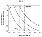
先ず、ある特定の誘電率の絶縁膜材料を用いて、得ることができる酸化膜換算膜厚を、図1を用いて説明する。図1は横軸が絶縁膜の比誘電率、縦軸が、各々の比誘電率の絶縁膜材料をある物理膜厚だけ成膜した場合に得られる酸化膜の換算膜厚の計算値を示す。パラメータは絶縁膜の物理膜厚である。絶縁膜材料として誘電率20の二酸化ハフニウムを、直接トンネルリーク電流を抑制可能な物理膜厚6nmに成膜した場合、図1より、薄膜化限界は約1.2nmである。図1での計算結果は、同構造で薄膜化を行なった場合、酸化膜換算膜厚1.2nm程度で直接トンネルリーク電流の増大に起因した薄膜化限界となることを示唆する。又、二酸化ハフニウムの物理膜厚を減少し、薄膜化を行なっていくと、絶縁膜のトンネル障壁の減少に起因した、Fowler-Nordheim (FN)トンネルリーク電流の増大も懸念される。特に、二酸化ハフニウムを、薄膜化限界である物理膜厚約6nm付近で使用する場合に問題が発生しやすいと考えられる。 First, an equivalent oxide film thickness that can be obtained using an insulating film material having a specific dielectric constant will be described with reference to FIG. In FIG. 1, the horizontal axis represents the relative dielectric constant of the insulating film, and the vertical axis represents the calculated value of the equivalent oxide film thickness obtained when the insulating film material having each relative dielectric constant is deposited to a certain physical film thickness. . The parameter is the physical film thickness of the insulating film. When hafnium dioxide having a dielectric constant of 20 is formed as an insulating film material to a physical film thickness of 6 nm capable of directly suppressing the tunnel leakage current, the thinning limit is about 1.2 nm as shown in FIG. The calculation result in FIG. 1 suggests that, when thinning is performed with the same structure, the oxide film thickness is about 1.2 nm, which is the limit of thinning directly due to an increase in tunnel leakage current. Further, when the physical film thickness of hafnium dioxide is reduced and the film thickness is reduced, there is a concern that the Fowler-Nordheim (FN) tunnel leakage current may increase due to the reduction of the tunnel barrier of the insulating film. In particular, it is considered that problems are likely to occur when hafnium dioxide is used in the vicinity of a physical film thickness of about 6 nm, which is the limit of thinning.
一方、量産の生産ラインに備えられている絶縁膜の成膜装置に対する投資額を抑制し、コスト低減を行うためには、同じ材料をできるだけ長い世代に適用することが望ましい。そのためにも、上部電極および下部電極に窒化チタンを用いたMIM構造の二酸化ハフニウムキャパシタがFNトンネルリーク電流増大に起因した薄膜化限界に達した場合、上部電極を、窒化チタンよりも仕事関数が大きいルテニウムで置き換えることが望ましい。この構成によって、FNトンネルリーク電流を抑制し、さらに薄膜化を進めることが可能であると考えられる。ルテニウムで、上部電極および下部電極を置き換えることも有用である。 On the other hand, it is desirable to apply the same material to the longest generation as much as possible in order to suppress the investment amount of the insulating film forming apparatus provided in the mass production line and reduce the cost. Therefore, when the hafnium dioxide capacitor with MIM structure using titanium nitride for the upper and lower electrodes reaches the limit of thinning due to the increase in FN tunnel leakage current, the work function of the upper electrode is larger than that of titanium nitride. It is desirable to replace with ruthenium. With this configuration, it is considered that the FN tunnel leakage current can be suppressed and the film thickness can be further reduced. It is also useful to replace the upper and lower electrodes with ruthenium.
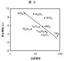
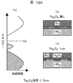
図2には、半導体向けの絶縁膜材料の候補が挙げられている。図2では、横軸と縦軸は、各々、比誘電率と禁性帯幅である。世代が進むにつれ高い誘電率が必要とされるが、リーク電流抑制のためには、大きな禁性帯幅も同時に必要である。しかし、図2から分かるように、比誘電率を増大すると禁性帯幅は減少する傾向があることが分かる。つまり、比誘電率が必要以上に大きな材料を用いると、禁性帯幅の狭さに起因したバリア高さの減少によりリーク電流抑制の観点から問題が生じる可能性がある。よって、各々の世代に用いる絶縁膜は、要求酸化膜換算膜厚の達成に必要な、適度な比誘電率を有する絶縁膜が望ましい。つまり、前述の酸化膜の換算膜厚1.2nm程度を得る場合、絶縁膜材料は二酸化ハフニウムが最も適した絶縁膜と言える。 In FIG. 2, candidates for insulating film materials for semiconductors are listed. In FIG. 2, the horizontal axis and the vertical axis represent the relative permittivity and the forbidden band width, respectively. As the generation progresses, a high dielectric constant is required, but a large forbidden bandwidth is also necessary to suppress leakage current. However, as can be seen from FIG. 2, the forbidden band tends to decrease as the relative dielectric constant increases. That is, if a material having a relative dielectric constant larger than necessary is used, there is a possibility that a problem arises from the viewpoint of suppressing leakage current due to a decrease in barrier height due to the narrow band gap. Therefore, the insulating film used for each generation is desirably an insulating film having an appropriate relative dielectric constant necessary for achieving the required equivalent oxide thickness. That is, when obtaining the above-mentioned equivalent oxide film thickness of about 1.2 nm, hafnium dioxide is the most suitable insulating film material.
<ルテニウムと二酸化ハフニウムとが直接接触する構造の問題点と、キャップ絶縁膜の必要性>
現在、DRAMに搭載するメモリセルキャパシタ向けには、リーク電流密度をおよそ10-7 A/cm2以下としなければならない。こうした条件に対して、上部電極にルテニウム、下部電極に窒化チタン、絶縁膜に二酸化ハフニウムを用いた構造のキャパシタが、どのようなリーク電流を有し、その原因は何かを検討した。そして、リーク電流の原因が、電極のルテニウムが絶縁膜の二酸化ハフニウム中に拡散していることであることを突きとめた。そこで、ルテニウムの拡散を抑制する方法として、ルテニウムと二酸化ハフニウムの界面に対して、キャップ層絶縁膜の挿入を検討した。
<Problem of structure in which ruthenium and hafnium dioxide are in direct contact, and necessity of cap insulating film>
Currently, for a memory cell capacitor mounted on a DRAM, the leakage current density must be about 10 −7 A / cm 2 or less. Under these conditions, a capacitor having a structure using ruthenium for the upper electrode, titanium nitride for the lower electrode, and hafnium dioxide for the insulating film has been examined for what leakage current and the cause. The inventors have determined that the cause of the leakage current is that the ruthenium of the electrode is diffused in the hafnium dioxide of the insulating film. Therefore, as a method for suppressing the diffusion of ruthenium, the insertion of a cap layer insulating film into the interface between ruthenium and hafnium dioxide was examined.
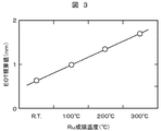
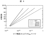
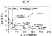
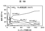
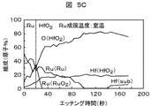
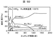
先ず、上部電極にルテニウム、下部電極に窒化チタン、絶縁膜に二酸化ハフニウムを用いた構造のキャパシタを試作し、電気特性および物理分析した結果を示す。図3は、ルテニウムの成膜温度とキャパシタの酸化膜の換算膜厚(ETO概算値)の関係を示す。成膜温度は、室温(R.T.)、100℃、200℃、300℃である。窒化チタンは化学気相成長法により30nm成膜し、二酸化ハフニウムは原子層成長法により10nm成膜、ルテニウムはスパッタ法により50nm成膜した。50%はおよそ、0.5nmと2.0nmの間に存在し、成膜温度の増大とともに増大する。又、リーク電流密度の累積度数分布の模式図を図4に示す。リーク電流密度の低いキャパシタは10-8A/cm -10-7A/cm2程度である、しかし、成膜温度の増大と共にばらつきは増大し、成膜温度300℃の場合は、リーク電流密度の大きなキャパシタは1 A/cm2程度である。前述したように、DRAMに搭載するメモリセルキャパシタ向けには、リーク電流密度をおよそ10-7 A/cm2以下としなければならない。この観点から、測定されたリーク電流は相当大きいと言わなければならない。 First, a capacitor having a structure using ruthenium for the upper electrode, titanium nitride for the lower electrode, and hafnium dioxide for the insulating film is manufactured, and the results of electrical characteristics and physical analysis are shown. FIG. 3 shows the relationship between the deposition temperature of ruthenium and the equivalent film thickness (ETO approximate value) of the capacitor oxide film. The film formation temperature is room temperature (RT), 100 ° C., 200 ° C., and 300 ° C. Titanium nitride was deposited to 30 nm by chemical vapor deposition, hafnium dioxide was deposited to 10 nm by atomic layer deposition, and ruthenium was deposited to 50 nm by sputtering. 50% is approximately between 0.5 nm and 2.0 nm, and increases as the film formation temperature increases. A schematic diagram of the cumulative frequency distribution of the leakage current density is shown in FIG. Capacitors with low leakage current density are about 10 −8 A / cm −10 −7 A / cm 2 , but the variation increases as the film formation temperature increases. When the film formation temperature is 300 ° C., the leakage current density A large capacitor is about 1 A / cm 2 . As described above, the leak current density must be about 10 −7 A / cm 2 or less for the memory cell capacitor mounted on the DRAM. From this point of view, it must be said that the measured leakage current is quite large.
このリーク電流ばらつきの原因を究明するために、X線光電子分光法による分析と、アルゴンイオンによる試料のエッチングを交互に行い、各試料の深さ方向の元素分析を行った。図5(A)より図5(D)にこの結果を示す。各図は各々、Ruの成膜温度を、200℃、300℃、室温、100℃とした場合の結果である。又、縦軸は原子パーセントで示した各元素および各結合の占める割合、横軸がエッチング時間である。ここで、材料によりエッチングの速度が異なることに注意が必要である。ルテニウムは0.15nm/秒程度であり、二酸化ハフニウムは0.05nm/秒程度である。検出された元素および結合状態は、金属ルテニウムに起因したルテニウム、二酸化ルテニウムに起因したルテニウム、二酸化ハフニウム起因したハフニウム、ハフニウムのサブピーク、二酸化ハフニウムに起因した酸素の5つである。点線で示したアルゴンイオンエッチング時間が20秒より短い表面付近では、金属ルテニウムが支配的に存在する。しかし、点線より深い位置では、二酸化ハフニウムに起因するハフニウム、および酸素の量が支配的となる。この傾向は予想された通りである。しかし、ここで注目したいのは、界面付近での元素の量の変化の仕方である。相互拡散などの無い急峻な界面が形成されている場合、点線で示した時間付近で、界面よりも表面側にある元素は急激に減少すると考えられ、又、それよりも試料の深い位置に存在する元素は急激に増加すると考えられる。実際、二酸化ルテニウム起因のルテニウムは、アルゴンイオンエッチング時間の増大に対して急激に減少している。一方、二酸化ハフニウム起因のハフニウムおよび酸素は、アルゴンイオンエッチング時間の増大に対して比較的急峻に増大している。ところが、金属ルテニウムに起因するルテニウムは、アルゴンイオン時間の増大に対して、これまで見てきた元素と同等の傾きで減少することが予想される。しかし、実際は傾斜がなだらかになっている。ルテニウムの成膜温度が室温の試料では、金属ルテニウムに起因するルテニウムの原子パーセントが10%以下となるのが、約90秒である。これは、ルテニウムが二酸化ハフニウム中に拡散していることを示唆している。又、ルテニウムの成膜時間を増大させると、金属ルテニウムの起因のルテニウムが検出される二酸化ハフニウム中の深さは増大している。ルテニウムの成膜温度を100℃、200℃、300℃と上昇させていくと、金属ルテニウム起因のルテニウムの原子パーセントが10%となる時間は、110秒、110秒、140秒と増大している。温度の上昇は拡散速度を増加させるため、この結果も、ルテニウムが二酸化ハフニウム中に拡散していると考えられる。よって、図4で示したリーク電流密度のばらつきを抑制するためには、ルテニウムが二酸化ハフニウム中に拡散するのを抑制する必要があると考えた。そこで、ルテニウムの拡散を抑制する方法として、ルテニウムと二酸化ハフニウムの界面に対して、キャップ層絶縁膜の挿入を検討した。 In order to investigate the cause of this variation in leakage current, analysis by X-ray photoelectron spectroscopy and etching of samples with argon ions were alternately performed, and elemental analysis in the depth direction of each sample was performed. The results are shown in FIG. 5A to FIG. 5D. Each figure shows the results when the deposition temperature of Ru is 200 ° C., 300 ° C., room temperature, and 100 ° C. In addition, the vertical axis represents the percentage of each element and each bond expressed in atomic percent, and the horizontal axis represents the etching time. Here, it should be noted that the etching rate differs depending on the material. Ruthenium is about 0.15 nm / second, and hafnium dioxide is about 0.05 nm / second. There are five detected elements and bonding states: ruthenium attributed to ruthenium metal, ruthenium attributed to ruthenium dioxide, hafnium attributed to hafnium dioxide, hafnium sub-peak, and oxygen attributed to hafnium dioxide. In the vicinity of the surface where the argon ion etching time indicated by the dotted line is shorter than 20 seconds, metallic ruthenium exists predominantly. However, at positions deeper than the dotted line, the amounts of hafnium and oxygen due to hafnium dioxide are dominant. This trend is as expected. However, what we want to pay attention to here is how the amount of elements changes near the interface. When a steep interface without interdiffusion is formed, the elements on the surface side of the interface are considered to decrease rapidly around the time indicated by the dotted line, and exist at a deeper position in the sample than that. It is considered that the number of elements to increase rapidly. In fact, ruthenium due to ruthenium dioxide decreases rapidly with increasing argon ion etching time. On the other hand, hafnium and oxygen resulting from hafnium dioxide increase relatively steeply as the argon ion etching time increases. However, it is expected that ruthenium resulting from the metal ruthenium will decrease with the same inclination as the elements that have been seen so far as the argon ion time increases. However, the slope is actually gentle. In a sample having a ruthenium film forming temperature of room temperature, the atomic percentage of ruthenium resulting from metal ruthenium is 10% or less in about 90 seconds. This suggests that ruthenium has diffused into hafnium dioxide. Further, when the ruthenium film formation time is increased, the depth in hafnium dioxide in which ruthenium attributable to metal ruthenium is detected increases. When the ruthenium film forming temperature is increased to 100 ° C., 200 ° C., and 300 ° C., the time when the atomic percentage of ruthenium caused by metal ruthenium is 10% increases to 110 seconds, 110 seconds, and 140 seconds. . Since the increase in temperature increases the diffusion rate, this result also suggests that ruthenium is diffusing into hafnium dioxide. Therefore, in order to suppress the variation in the leakage current density shown in FIG. 4, it was considered necessary to suppress the diffusion of ruthenium into hafnium dioxide. Therefore, as a method for suppressing the diffusion of ruthenium, the insertion of a cap layer insulating film into the interface between ruthenium and hafnium dioxide was examined.
<キャップ層絶縁膜として酸化タンタルが好ましい理由>
キャップ層絶縁膜の挿入により懸念されることとしては、酸化膜換算膜厚の増大、二酸化ハフニウムのバリアハイトの低下である。キャップ層絶縁膜を挿入するということは絶縁膜の膜厚増大につながるため、酸化膜換算膜厚が増大する。ルテニウムの二酸化ハフニウム中への拡散防止目的の場合、当材料同士が接触しないように、均一に成膜できる最小の膜厚だけのキャップ層絶縁膜を挿入すれば良い。
<Reason why tantalum oxide is preferable as the cap layer insulating film>
What is concerned about the insertion of the cap layer insulating film is an increase in the equivalent oxide thickness and a decrease in the barrier height of hafnium dioxide. Inserting the cap layer insulating film leads to an increase in the thickness of the insulating film, and thus the equivalent oxide thickness increases. For the purpose of preventing diffusion of ruthenium into hafnium dioxide, a cap layer insulating film having a minimum thickness that can be uniformly formed may be inserted so that the materials do not contact each other.
この時、その膜厚はおよそ2nmである。2nm以下では、いずれの成膜方法を用いても島状に成長し、均一な膜とならず、キャップ層の効果は無いと考えられる。同じ物理膜厚2nmだけ成膜するとしても、誘電率が大きな材料を用いた方が、酸化膜換算膜厚の増大は抑制できる。よって、キャップ層絶縁膜には、ルテニウムの二酸化ハフニウム中への拡散を抑制することに加え、キャパシタの酸化膜換算膜厚の増大を最小限とするために、誘電率の比較的大きな材料が好ましいと考えられる。又、本構造のキャパシタにおいて、2nmのキャップ層絶縁膜を挿入した場合であっても、Fowler-Nordheimトンネル電流や、直接トンネル電流に寄与する絶縁膜は、膜厚の厚い二酸化ハフニウムである。よって、これらリーク電流の抑制には、二酸化ハフニウムと電極間のバリア高さが重要となる。キャップ層絶縁膜を挿入した場合、キャップ層絶縁膜の材料に依存して二酸化ハフニウムのバリア高さが影響を受ける可能性があるが、キャップ層絶縁膜挿入により、二酸化ハフニウムのバリア高さがより高く保てるキャップ層絶縁膜材料が望ましい。よって、これらの観点からキャップ層絶縁膜の検討結果を示し、最適なキャップ層絶縁膜を例示す。 At this time, the film thickness is about 2 nm. If it is 2 nm or less, it is considered that any film forming method grows in an island shape and does not form a uniform film, and there is no effect of the cap layer. Even if the same physical film thickness is 2 nm, an increase in the equivalent oxide film thickness can be suppressed by using a material having a large dielectric constant. Therefore, a material having a relatively large dielectric constant is preferable for the cap layer insulating film in order to suppress the diffusion of ruthenium into hafnium dioxide and minimize the increase in equivalent oxide thickness of the capacitor. it is conceivable that. Further, in the capacitor of this structure, even when a 2 nm cap layer insulating film is inserted, the Fowler-Nordheim tunnel current or the insulating film directly contributing to the tunnel current is thick hafnium dioxide. Therefore, the barrier height between hafnium dioxide and the electrode is important for suppressing these leakage currents. When a cap layer insulating film is inserted, the barrier height of hafnium dioxide may be affected depending on the material of the cap layer insulating film. However, the insertion of the cap layer insulating film further increases the barrier height of hafnium dioxide. A cap layer insulating film material that can be kept high is desirable. Therefore, the examination result of the cap layer insulating film is shown from these viewpoints, and the optimum cap layer insulating film is shown as an example.
《キャップ層絶縁膜としての、五酸化タンタルとアルミナとの比較検討》
キャップ層絶縁膜として、候補と目される五酸化タンタルとアルミナとを比較検討した。両者はリーク電流のばらつきを抑制する効果は同等であるが、キャップ層絶縁膜がキャパシタ用絶縁膜の、二酸化ハフニウムのバリアの高さをより大きく取ることを可能にする。このことから、五酸化タンタルが最適の材用である。同様の観点で、酸化ニオブも好適である。こうしたバンド構造の問題は後に詳述する。
《Comparison study of tantalum pentoxide and alumina as cap layer insulating film》
As a cap layer insulating film, tantalum pentoxide, which is a candidate, was compared with alumina. Both of them have the same effect of suppressing the variation in leakage current, but the cap layer insulating film makes it possible to increase the height of the hafnium dioxide barrier of the capacitor insulating film. For this reason, tantalum pentoxide is the most suitable material. From the same viewpoint, niobium oxide is also suitable. The problem of such a band structure will be described in detail later.
キャップ層絶縁膜の材料の候補として挙げるのは、五酸化タンタルとアルミナである。共に半導体プロセスとして広く検討され、用いられている材料である。これらの材料は、更に、高アスペクトのキャパシタにも成膜できる技術が確立しているため、DRAMキャパシタに適用可能な材料である。 Candidate materials for the cap layer insulating film are tantalum pentoxide and alumina. Both materials are widely studied and used as semiconductor processes. These materials can be applied to DRAM capacitors because a technique capable of forming a film on a high aspect capacitor has been established.
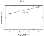
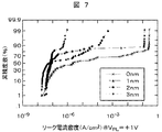
キャップ層絶縁膜に五酸化タンタルを用いたキャパシタの、酸化膜換算膜厚の概算値のキャップ層絶縁膜膜厚依存性を図6に示す。およそ、キャップ層絶縁膜の膜厚の増大に伴い、酸化膜換算膜厚が増大している。傾きより求めた比誘電率は約26である。次に、リーク電流密度の、キャップ層絶縁膜膜厚依存性を図7に示す。キャップ層絶縁膜膜厚を増大していくと、リーク電流密度ばらつきが劇的に減少していることが分かる。五酸化タンタルの膜厚が2nmでは、リーク電流密度のばらつきは約4桁、3nmの場合には約2桁である。つまり、五酸化タンタルキャップ層絶縁膜の挿入は、リーク電流密度のばらつき抑制には非常に効果的であることが判明した。 FIG. 6 shows the dependence of the approximate oxide film thickness on the cap layer insulating film thickness of a capacitor using tantalum pentoxide as the cap layer insulating film. As the thickness of the cap layer insulating film increases, the equivalent oxide thickness increases. The relative dielectric constant obtained from the slope is about 26. Next, FIG. 7 shows the dependence of the leakage current density on the cap layer insulating film thickness. It can be seen that as the cap layer insulating film thickness is increased, the leakage current density variation is dramatically reduced. When the film thickness of tantalum pentoxide is 2 nm, the variation in the leakage current density is about 4 digits, and when it is 3 nm, it is about 2 digits. That is, it has been found that the insertion of the tantalum pentoxide cap layer insulating film is very effective in suppressing variation in leakage current density.
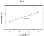
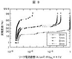
次にキャップ層絶縁膜にアルミナを用いた場合の、酸化膜換算膜厚概算値の、キャップ層絶縁膜膜厚依存性を図8に示す。酸化膜換算膜厚は、アルミナの膜厚を増大すると増大する傾向にある。傾きより、比誘電率を導出すると約9.4であった。五酸化タンタルをキャップ層絶縁膜に用いた場合と比較すると、比誘電率の差に起因して、挿入したキャップ層絶縁膜の物理膜厚に対する酸化膜換算膜厚の増加率が大きいことが分かる。アルミナをキャップ層絶縁膜に用いた場合、比誘電率の低さに起因した、酸化膜換算膜厚の増大が、実際に観察された。次に、リーク電流密度の、キャップ層絶縁膜膜厚依存性を図9に示す。アルミナ膜厚3nmの試料を除くと、キャップ層絶縁膜の膜厚を増大させると、リーク電流ばらつきが減少する傾向が確認された。キャップ層絶縁膜としてアルミナを挿入しない場合、8桁であったリーク電流密度のばらつきは、アルミナを2nm挿入することで3桁まで減少できた。つまり、五酸化タンタルを挿入した場合と同様に、アルミナをキャップ層絶縁膜に用いてもリーク電流密度のばらつきは同様に低減することが可能である。 Next, FIG. 8 shows the dependence of the equivalent oxide film thickness on the cap layer insulating film thickness when alumina is used for the cap layer insulating film. The equivalent oxide thickness tends to increase as the alumina thickness increases. From the slope, the relative dielectric constant was derived to be about 9.4. Compared with the case where tantalum pentoxide is used for the cap layer insulating film, it can be seen that the increase rate of the equivalent oxide thickness with respect to the physical thickness of the inserted cap layer insulating film is larger due to the difference in relative dielectric constant. . When alumina was used for the cap layer insulating film, an increase in equivalent oxide thickness due to the low relative dielectric constant was actually observed. Next, the dependence of the leakage current density on the cap layer insulating film thickness is shown in FIG. Excluding the sample with an alumina film thickness of 3 nm, it was confirmed that when the film thickness of the cap layer insulating film was increased, the variation in leakage current was reduced. When alumina was not inserted as the cap layer insulating film, the variation in leakage current density, which was 8 digits, could be reduced to 3 digits by inserting 2 nm of alumina. That is, similarly to the case where tantalum pentoxide is inserted, even if alumina is used for the cap layer insulating film, the variation in the leakage current density can be similarly reduced.
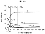
そこで、実際にキャップ層絶縁膜の挿入により、ルテニウムの二酸化ハフニウム中への拡散が抑制されていることを確認するために、キャップ層絶縁膜に五酸化タンタルを2nm挿入した試料を用いて、図5で示した、X線光電子分光法とアルゴンイオンエッチングを組み合わせた実験を行い、含有元素の深さプロファイルを取得した。その結果を図10に示す。アルゴンイオンエッチング時間が20秒までが電極ルテニウム、60秒までがキャップ層絶縁膜五酸化タンタル、60秒以降が二酸化ハフニウムをエッチングしていると考えられる。図10より、五酸化タンタルキャップ層絶縁膜2nmの挿入により、ルテニウムの二酸化ハフニウム中への拡散が劇的に減少していることが分かる。五酸化タンタルと二酸化ハフニウムの界面では、金属ルテニウム起因のルテニウムの原子パーセントは10%以下となっている。つまり、五酸化タンタルをキャップ層絶縁膜に用いると、ルテニウムの二酸化ハフニウム中への拡散が抑制され、リーク電流密度のばらつきが抑制されたと考えられる。 Therefore, in order to confirm that the diffusion of ruthenium into hafnium dioxide is actually suppressed by the insertion of the cap layer insulating film, a sample in which 2 nm of tantalum pentoxide is inserted into the cap layer insulating film is used. Experiments combining X-ray photoelectron spectroscopy and argon ion etching shown in FIG. 5 were conducted, and depth profiles of the contained elements were obtained. The result is shown in FIG. It is considered that the argon ion etching time is etching the electrode ruthenium up to 20 seconds, the cap layer insulating film tantalum pentoxide up to 60 seconds, and the hafnium dioxide etching after 60 seconds. FIG. 10 shows that the diffusion of ruthenium into hafnium dioxide is dramatically reduced by the insertion of the tantalum pentoxide cap layer insulating film of 2 nm. At the interface between tantalum pentoxide and hafnium dioxide, the atomic percentage of ruthenium due to metal ruthenium is 10% or less. That is, it is considered that when tantalum pentoxide is used for the cap layer insulating film, diffusion of ruthenium into hafnium dioxide is suppressed, and variation in leakage current density is suppressed.
以上の結果より、五酸化タンタルをルテニウム上部電極と二酸化ハフニウム絶縁膜の間に挿入するキャップ層絶縁膜として用いると、ルテニウムの二酸化ハフニウム中への拡散が抑制されることが明らかとなった。 From the above results, it was found that when tantalum pentoxide is used as a cap layer insulating film inserted between the ruthenium upper electrode and the hafnium dioxide insulating film, diffusion of ruthenium into hafnium dioxide is suppressed.
五酸化タンタルの比誘電率(26)は二酸化ハフニウムの比誘電率(20)よりも大きいことを考慮すると、絶縁膜を全て五酸化タンタルに置き換える方法も考えられるが、同方法は有効ではない。それは、五酸化タンタルはルテニウムとは急峻な界面を形成するが、窒化チタンと接触させると互いに反応し、急峻な界面が得られないからである。つまり、窒化チタンとの界面には二酸化ハフニウムが接していることが望ましい。下部電極をルテニウムとすれば、絶縁膜を五酸化タンタル単層とすることができるが、ルテニウムを下部電極に用いるためには、上部電極に用いるよりも高い技術が必要である。よって、技術的課題の少ない上部電極にルテニウムを適用する世代では、下部電極には広く用いられている窒化チタンを用いる必要がある。 Considering that the relative dielectric constant (26) of tantalum pentoxide is larger than the relative dielectric constant (20) of hafnium dioxide, a method of replacing all of the insulating film with tantalum pentoxide can be considered, but this method is not effective. This is because tantalum pentoxide forms a steep interface with ruthenium, but when it comes into contact with titanium nitride, it reacts with each other and a steep interface cannot be obtained. That is, it is desirable that hafnium dioxide is in contact with the interface with titanium nitride. If the lower electrode is made of ruthenium, the insulating film can be a single layer of tantalum pentoxide. However, in order to use ruthenium for the lower electrode, a technique higher than that used for the upper electrode is required. Therefore, in the generation in which ruthenium is applied to the upper electrode with few technical problems, it is necessary to use titanium nitride which is widely used for the lower electrode.
このような観点から、キャップ層絶縁膜材料として考えられる他の材料は、酸化ニオブが挙げられる。当材料の比誘電率は30程度であり、同様のキャップ層の効果があると考えられる。 From such a viewpoint, niobium oxide is another material that can be considered as the cap layer insulating film material. The relative dielectric constant of this material is about 30, and it is considered that the same cap layer effect is obtained.
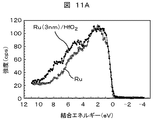
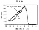
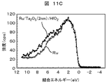
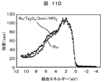
次に、ルテニウムが二酸化ハフニウム中に拡散することにより、リーク電流密度のばらつきを生じるメカニズムを説明する。五酸化タンタルを0nmから3nmまで1nmおきに増大させていった4つの試料をX線光電子分光法により分析し、得られた価電子帯波形を結果を図11Aより図11Dに示す。各々の図には、ルテニウムを50nm成膜した試料の分析から得られた、ルテニウムのみから得られた価電子帯波形を重ねて示す。価電子帯波形において、結合エネルギー0eVはフェルミエネルギーに対応し、結合エネルギーが増大すると、フェルミエネルギーよりも深いエネルギー準位を示す。また、価電子帯波形の強度は、その準位における電子の状態密度を示す。ルテニウムのみからの価電子帯波形と、二酸化ハフニウムとルテニウムを積層したときの波形の差分は、二酸化ハフニウムの状態密度を示す。図11(a)はキャップ層絶縁膜を挿入していない試料の結果であるが、結合エネルギーは約2.5eVから差分が生じている。この差分が生じ始めているエネルギーは価電子帯の上端に対応し、ルテニウムのフェルミエネルギーと二酸化ハフニウムの価電子帯オフセットが2.5eVであることを示す。このように考えると、どの試料においても、価電子帯上端のエネルギーよりも低いエネルギーではルテニウムのみに起因した波形と二酸化ハフニウムおよびキャップ層絶縁膜の五酸化タンタルを積層した試料の波形は重ならなくてはいけない。それは、このエネルギーは絶縁膜の禁性帯に対応するため、絶縁膜の状態密度は存在しないからである。しかし、図11A−図11Dを見ると、キャップ層絶縁膜が無い試料(図11A)および1nmの試料(図11B)については、結合エネルギー1eV−2eVの間に、同スペクトルの差分が発生している。一方、五酸化タンタルキャップ層絶縁膜を2nm以上挿入すると、同差分は消滅している。つまり、ルテニウムが二酸化ハフニウムに拡散していることが確認されている、キャップ層絶縁膜無しの試料では、二酸化ハフニウムの禁性帯中に何らかの状態密度が発生しており、一方、同拡散の抑制が確認されているキャップ層絶縁膜五酸化タンタルの膜厚が2nm以上の試料に関しては、同二酸化ハフニウムの禁性帯中の準位は消えていることが分かった。この結果は次のように考えることができる。
Next, a mechanism that causes variation in the leakage current density due to diffusion of ruthenium into hafnium dioxide will be described. Four samples in which tantalum pentoxide was increased from 0 nm to 3 nm every 1 nm were analyzed by X-ray photoelectron spectroscopy, and the valence band waveforms obtained are shown in FIGS. 11A to 11D. In each figure, the valence band waveform obtained only from ruthenium obtained by analyzing a sample in which ruthenium is deposited to 50 nm is superimposed and shown. In the valence band waveform, the binding energy of 0 eV corresponds to the Fermi energy, and when the binding energy increases, the energy level is deeper than the Fermi energy. The intensity of the valence band waveform indicates the density of states of electrons at that level. The difference between the valence band waveform from only ruthenium and the waveform when hafnium dioxide and ruthenium are laminated indicates the density of states of hafnium dioxide. FIG. 11A shows the result of the sample in which the cap layer insulating film is not inserted, but the binding energy has a difference from about 2.5 eV. The energy at which this difference begins to occur corresponds to the upper end of the valence band, indicating that the fermi energy of ruthenium and the valence band offset of hafnium dioxide are 2.5 eV. In this way, in any sample, the waveform due to ruthenium alone and the waveform of the sample laminated with hafnium dioxide and tantalum pentoxide of the cap layer insulating film do not overlap at energy lower than the energy at the top of the valence band. must not. This is because there is no density of states of the insulating film because this energy corresponds to the forbidden band of the insulating film. However, as shown in FIGS. 11A to 11D, for the sample without the cap layer insulating film (FIG. 11A) and the 1 nm sample (FIG. 11B), a difference in the same spectrum occurs between the
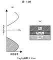
図12A及び図12Bには状態密度およびキャパシタの模式図を示した。キャップ層絶縁膜の五酸化タンタルの膜厚が1nm以下の場合、つまり五酸化タンタルが無い図12Aの(b)又は、1nmの膜のように均一な膜となっておらずルテニウムと二酸化ハフニウムが接している部分が存在する場合(図12Aの(c))は、ルテニウムが二酸化ハフニウム中に拡散し、二酸化ハフニウムの禁性帯中に状態密度を作ったと考えられる(図12Aの(a))。一方、キャップ層絶縁膜の五酸化タンタルの膜厚が2nm以上の場合(図12Bの(e))、つまり、均一な膜であるキャップ層絶縁膜の五酸化タンタルによりルテニウムと二酸化ハフニウムが完全に隔てられている場合、ルテニウムの二酸化ハフニウム中への拡散は抑制され、二酸化ハフニウムの禁性帯中には状態密度の発生は無いと考えられる(図12Bの(a))。 12A and 12B are schematic diagrams of density of states and capacitors. When the film thickness of tantalum pentoxide of the cap layer insulating film is 1 nm or less, that is, (b) in FIG. 12A without tantalum pentoxide or a uniform film as in the 1 nm film, ruthenium and hafnium dioxide are not formed. When there is a contact portion ((c) in FIG. 12A), it is considered that ruthenium diffuses into hafnium dioxide and creates a density of states in the forbidden band of hafnium dioxide ((a) in FIG. 12A). . On the other hand, when the film thickness of the tantalum pentoxide of the cap layer insulating film is 2 nm or more ((e) in FIG. 12B), that is, the tantalum pentoxide of the cap layer insulating film which is a uniform film completely causes ruthenium and hafnium dioxide to completely disappear. When separated, the diffusion of ruthenium into hafnium dioxide is suppressed, and it is considered that no density of states is generated in the forbidden band of hafnium dioxide (FIG. 12B (a)).
《キャップ層絶縁膜の二酸化ハフニウムのバリア高さに与える影響》
次に、キャップ層絶縁膜の挿入による、二酸化ハフニウムのバリア高さに与える影響を説明する。同評価のために、キャップ層絶縁膜に五酸化タンタル、またはアルミナを3nm挿入した場合のバンド構造を、物理分析により導出した。
<Effect of cap layer insulating film on barrier height of hafnium dioxide>
Next, the influence of the insertion of the cap layer insulating film on the barrier height of hafnium dioxide will be described. For the same evaluation, a band structure in the case where 3 nm of tantalum pentoxide or alumina was inserted into the cap layer insulating film was derived by physical analysis.
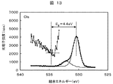
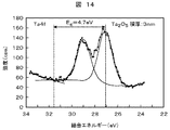
図13では、二酸化ハフニウムに起因したO1sピークの波形を示す。O1sのメインピークのエネルギーと、高エネルギー側に現れるロスピークの立ち上がりのエネルギーの差が、二酸化ハフニウムの禁性帯幅に一致することが知られている。同方法により求めた、二酸化ハフニウムの禁性帯幅は4.4eVであった。この値は、一般的に報告されている値よりも小さいが、これは、成膜方法等が最適化されていないためと考えられる。最適化を行なうと、二酸化ハフニウムの禁性帯幅は6.0eVとなる。
次に図14では五酸化タンタルに起因したTa4fピークの波形を示す。Ta4fのピークエネルギーとロスピークの立ち上がりのエネルギー差より、五酸化タンタルの禁性帯幅を導出すると、4.7eVであった。
In FIG. 13, the waveform of the O1s peak resulting from hafnium dioxide is shown. It is known that the difference between the energy of the main peak of O1s and the energy of the rise of the loss peak that appears on the high energy side matches the band gap of hafnium dioxide. The forbidden band width of hafnium dioxide determined by the same method was 4.4 eV. This value is smaller than a generally reported value, which is considered to be because the film forming method or the like is not optimized. When optimized, the band gap of hafnium dioxide is 6.0 eV.
Next, FIG. 14 shows the waveform of the Ta4f peak due to tantalum pentoxide. The band gap of tantalum pentoxide was derived from the difference in energy between the peak energy of Ta4f and the rise of the loss peak, and was 4.7 eV.
次に、図11に示したキャップ層絶縁膜に五酸化タンタルを挿入した試料およびアルミナを挿入した試料より得られた価電子帯波形から求めた、絶縁膜の価電子帯上端のエネルギーをまとめたのが図15である。五酸化タンタルおよびアルミナの膜厚を増大していくと、価電子帯オフセットの値は徐々に増大していく。これは、十分膜厚の厚い、ルテニウムと二酸化ハフニウムを積層したときの価電子帯オフセットが、ルテニウムと五酸化タンタルまたはアルミナを積層した時の価電子帯オフセットの値が変化している様子が見えていると考えられる。キャップ層絶縁膜の膜厚を3nm程度にすると、キャップ層絶縁膜材料のバルクの値に近いバンド構造が出来ると考えられる。また、特にアルミナを挿入すると価電子帯オフセットの増加量は大きい。これは、アルミナの禁性帯幅が6.6eVと比較的大きいため、アルミナの価電子帯オフセットも五酸化タンタルに比べて大きいためと考えられる。 Next, the energy at the top of the valence band of the insulating film obtained from the valence band waveform obtained from the sample in which tantalum pentoxide was inserted into the cap layer insulating film and the sample in which alumina was inserted as shown in FIG. This is shown in FIG. As the film thicknesses of tantalum pentoxide and alumina are increased, the value of the valence band offset gradually increases. This shows that the valence band offset when ruthenium and hafnium dioxide are stacked is sufficiently thick, but the valence band offset value when ruthenium and tantalum pentoxide or alumina are stacked changes. It is thought that. It is considered that when the thickness of the cap layer insulating film is about 3 nm, a band structure close to the bulk value of the cap layer insulating film material can be formed. In particular, when alumina is inserted, the increase in valence band offset is large. This is presumably because alumina has a relatively large forbidden band width of 6.6 eV, so that the valence band offset of alumina is also larger than that of tantalum pentoxide.
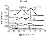
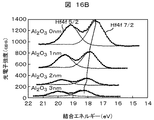
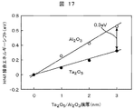
次に、キャップ層絶縁膜として五酸化タンタルとアルミナを、0nmから3nm挿入したときのHf4fピークの波形を、各々図16Aより図16Bに示す。これらの結果より分かるのは、いずれのキャップ層絶縁膜であっても、膜厚を増大していくと、Hf4fのピークエネルギーは高エネルギー側にシフトしていく点である。このピークエネルギーのシフト量をまとめたのが図17である。五酸化タンタルを挿入した場合もアルミナを挿入した場合も、キャップ層絶縁膜の物理膜厚増加に対してほぼ線形にHf4fのピークシフトが発生している。五酸化タンタルをキャップ層に3nm挿入した場合、約0.3eVの、アルミナをキャップ層絶縁膜に3nm挿入した場合、約0.6eVのシフトが観察された。このエネルギーシフトが意味するのは、ルテニウムに近い側の二酸化ハフニウムのバンドが、フェルミエネルギーに対してエネルギーシフトの分だけ下がっていることを示す。よって、キャップ層絶縁膜に五酸化タンタルを3nm挿入すると、アルミナを3nm挿入した場合に比べて、ルテニウム側の二酸化ハフニウムのバリア高さは0.3eV大きく取ることができることが判明した。 Next, waveforms of Hf4f peaks when tantalum pentoxide and alumina are inserted as cap layer insulating films from 0 nm to 3 nm are shown in FIGS. 16A and 16B, respectively. From these results, it is understood that the peak energy of Hf4f shifts to the higher energy side as the film thickness increases in any cap layer insulating film. FIG. 17 summarizes the shift amounts of the peak energy. In both cases where tantalum pentoxide is inserted and alumina is inserted, the peak shift of Hf4f occurs almost linearly with the increase in the physical film thickness of the cap layer insulating film. When tantalum pentoxide was inserted into the cap layer at 3 nm, a shift of about 0.3 eV was observed, and when alumina was inserted at 3 nm into the cap layer insulating film, a shift of about 0.6 eV was observed. This energy shift means that the hafnium dioxide band on the side closer to ruthenium is lower than the Fermi energy by the energy shift. Accordingly, it was found that when 3 nm of tantalum pentoxide is inserted into the cap layer insulating film, the barrier height of hafnium dioxide on the ruthenium side can be increased by 0.3 eV compared to the case where 3 nm of alumina is inserted.
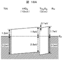
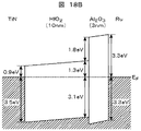
ルテニウムの仕事関数を4.8eV、窒化チタンの仕事関数を4.2eVと仮定すると、キャップ層絶縁膜として五酸化タンタルおよびアルミナを3nm挿入した場合のバンド構造は、各々図18A及び図18Bのように示すことができる。先に述べたように、二酸化ハフニウムのバリア高さはリーク電流への寄与が大きい。同バリア高さが大きいほど、リーク電流を低減することが可能である。このような観点からキャップ層絶縁膜を考えると、キャップ層絶縁膜にアルミナを用いた場合よりも五酸化タンタルを用いるほうが、二酸化ハフニウムのバリア高さを高くすることが可能であり、リーク電流低減に効果的であると考えられる。 Assuming that the work function of ruthenium is 4.8 eV and the work function of titanium nitride is 4.2 eV, the band structures when 3 nm of tantalum pentoxide and alumina are inserted as the cap layer insulating film are as shown in FIGS. 18A and 18B, respectively. Can be shown. As described above, the barrier height of hafnium dioxide greatly contributes to the leakage current. As the barrier height increases, the leakage current can be reduced. Considering the cap layer insulating film from this point of view, it is possible to increase the barrier height of hafnium dioxide by using tantalum pentoxide than when alumina is used for the cap layer insulating film, thereby reducing leakage current. It is considered effective.
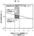
図19には、キャップ層絶縁膜膜厚と、得られる酸化膜換算膜厚の関係を示した。横軸が比誘電率25を仮定した五酸化タンタルキャップ層絶縁膜の物理膜厚、縦軸が図中に記載の絶縁膜の物理膜厚を、五酸化タンタル絶縁膜の物理膜厚と併せて、直接トンネルリーク電流を抑制に最低限必要な6nmとしたときの酸化膜換算膜厚を示している。また、図中の黒点は、キャップ層絶縁膜および絶縁膜の膜厚を、最低それぞれ均一な膜となる2nm以上としたときの、実現可能な酸化膜換算膜厚を示している。絶縁膜に比誘電率20の二酸化ハフニウムを用いた場合、酸化膜換算膜厚は1.2nm以下で作成可能である。特に、キャップ層絶縁膜に五酸化タンタル2nmを適用しても、酸化膜換算膜厚1.2nm以下で、直接トンネルリーク電流を抑制したキャパシタの作成が可能であることが分かった。また、絶縁膜に比誘電率25の酸化ジルコニウムを用いた場合、同様に1.0nm以下の酸化膜換算膜厚のキャパシタを作成可能であり、キャップ層に五酸化タンタルを用いても、薄膜化限界はほぼ同等である。つまり、五酸化タンタルは二酸化ハフニウムや二酸化ジルコニウムよりも誘電率が高いため、キャップ層の挿入により、薄膜化限界が増大するようなことは無い。つまり、キャパシタ絶縁膜よりも誘電率の大きな材料からなるキャップ層の適用は、両者の物理膜厚の和が同じになるようにして積層しても、酸化膜換算膜厚の増大、もしくは容量の損失無くキャパシタ形成することができるため、非常に有効であることがわかった。 FIG. 19 shows the relationship between the cap layer insulating film thickness and the equivalent oxide film thickness obtained. The horizontal axis represents the physical film thickness of the tantalum pentoxide cap layer insulating film assuming a relative dielectric constant of 25, and the vertical axis represents the physical film thickness of the insulating film described in the figure together with the physical film thickness of the tantalum pentoxide insulating film. The oxide film equivalent film thickness is shown when the direct tunnel leakage current is 6 nm, which is the minimum necessary for suppression. The black dots in the figure indicate the equivalent oxide film thickness that can be achieved when the cap layer insulating film and the insulating film have a minimum thickness of 2 nm or more, which is a uniform film. When hafnium dioxide with a relative dielectric constant of 20 is used for the insulating film, the oxide film equivalent film thickness can be made to be 1.2 nm or less. In particular, it has been found that even when tantalum pentoxide of 2 nm is applied to the cap layer insulating film, it is possible to produce a capacitor having a reduced oxide film thickness of 1.2 nm or less and directly suppressing a tunnel leakage current. In addition, when zirconium oxide having a relative dielectric constant of 25 is used for the insulating film, a capacitor having an equivalent oxide thickness of 1.0 nm or less can be similarly produced. Even if tantalum pentoxide is used for the cap layer, the thickness can be reduced. The limits are almost equivalent. That is, since tantalum pentoxide has a higher dielectric constant than hafnium dioxide or zirconium dioxide, the insertion of the cap layer does not increase the thinning limit. In other words, the application of a cap layer made of a material having a dielectric constant larger than that of the capacitor insulating film can increase the equivalent oxide film thickness or increase the capacitance even if they are laminated so that the sum of the physical film thicknesses of the two is the same. Since the capacitor can be formed without loss, it has been found to be very effective.
以上の結果より、キャップ層絶縁膜の材料は、従来材料のアルミナに比べ、五酸化タンタルが望ましいことが判明した。キャップ層絶縁膜の膜厚は拡散防止であるため、連続膜となっていなくてはならない。即ち、キャップ層絶縁膜は、連続膜となる最低の膜厚となして十分である。現実的には2nm以上である。また、絶縁膜の膜厚も同様に、連続膜となるためには2nm以上必要である。 From the above results, it was found that the material of the cap layer insulating film is preferably tantalum pentoxide as compared with the conventional material alumina. Since the film thickness of the cap layer insulating film is to prevent diffusion, it must be a continuous film. That is, the cap layer insulating film is sufficient as the minimum film thickness that can be a continuous film. Actually, it is 2 nm or more. Similarly, the thickness of the insulating film needs to be 2 nm or more in order to be a continuous film.
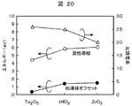
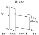
図20には、絶縁膜およびキャップ層絶縁膜の候補として挙げた材料の内一部の、禁性帯幅、伝導体オフセット量、および比誘電率の値を示した。一般的に、絶縁膜の絶縁性を示す指標をして用いられるのが、その絶縁膜材料の禁性帯幅である。五酸化タンタルの禁性帯幅は、二酸化ハフニウムや二酸化ジルコニウムに比べて小さい。しかし、キャパシタを作り、キャリアが電子と考えられる場合、各々のキャリアの絶縁膜中の伝導メカニズム(Fowler-Nordheimトンネル電流等)に関連しているのは、伝導帯オフセットである。これらの値はキャリアに対してバリアとして働くため、値が大きいほど、絶縁性能が高いと考えられる。図20より、キャップ層絶縁膜に用いる五酸化タンタルは、絶縁膜材料である二酸化ハフニウムや二酸化ジルコニウムに比べて伝導体オフセット量が小さいことがわかる。以上の事実および推測より、五酸化タンタルキャップ層絶縁膜と絶縁膜を積層したときFowler-Nordheimトンネル電流抑制に効果があるのは、絶縁膜である二酸化ハフニウム、または二酸化ジルコニウムである。ここで、電極および絶縁膜と、絶縁膜よりも伝導体オフセットの小さなキャップ層絶縁膜を積層したキャパシタの、キャップ層絶縁膜と接触している側の電極に正の電圧を印加した時のバンド構造を示したのが、図21A及び図21Bである。図21Aのように、もし、二酸化ハフニウムや二酸化ジルコニウム等の伝導体オフセット量の大きな絶縁膜材料の膜厚が薄いと、電極に電圧を印加した場合、電極中の電子が絶縁膜をトンネル効果により通り抜け、図21に示したように、伝導体オフセット量の小さなキャップ層絶縁膜の伝導体中を移動し、もう一方の電極に到達し、リーク電流を増大させる恐れがある。一方、図21Bのように伝導体オフセット量の大きな絶縁膜の物理膜厚が厚いと、電極より絶縁膜を通してキャップ層絶縁膜中に対して流れるF-Nトンネルリーク電流が抑制され、キャパシタのリーク電流も抑制されると考えられる。つまり、キャパシタ絶縁膜として異なる絶縁膜材料を積層する場合、価電子帯オフセット量の大きい絶縁膜の膜厚は、直接トンネルリーク電流が顕著な膜厚である6nm以下の範囲においては、厚くすべきである。先に、キャップ層絶縁膜の膜厚範囲は先に2nm以上3nm以下が望ましいと述べた。キャップ層絶縁膜材料の伝導体オフセット量が、絶縁膜材料の伝導体オフセット量よりも小さい場合は、キャップ層絶縁膜の膜厚は、絶縁膜の膜厚よりも薄くすると、リーク電流が抑制できるため、望ましい。 FIG. 20 shows the values of the forbidden band width, the conductor offset amount, and the relative dielectric constant of some of the materials listed as candidates for the insulating film and the cap layer insulating film. In general, it is the forbidden bandwidth of the insulating film material that is used as an index indicating the insulating property of the insulating film. The forbidden band width of tantalum pentoxide is smaller than that of hafnium dioxide and zirconium dioxide. However, when a capacitor is formed and the carriers are considered to be electrons, the conduction band offset is related to the conduction mechanism (Fowler-Nordheim tunnel current, etc.) in the insulating film of each carrier. Since these values act as a barrier against carriers, it is considered that the larger the value, the higher the insulation performance. From FIG. 20, it can be seen that tantalum pentoxide used for the cap layer insulating film has a smaller conductor offset amount than hafnium dioxide and zirconium dioxide, which are insulating film materials. From the above facts and assumptions, when the tantalum pentoxide cap layer insulating film and the insulating film are laminated, it is hafnium dioxide or zirconium dioxide that is effective in suppressing the Fowler-Nordheim tunnel current. Here, the band when a positive voltage is applied to the electrode in contact with the cap layer insulating film of the capacitor in which the electrode and the insulating film are laminated with the cap layer insulating film having a conductor offset smaller than that of the insulating film. The structure is shown in FIGS. 21A and 21B. As shown in FIG. 21A, if the insulating film material having a large conductor offset amount such as hafnium dioxide or zirconium dioxide is thin, when a voltage is applied to the electrode, electrons in the electrode cause the insulating film to pass through the tunnel effect. As shown in FIG. 21, there is a risk of moving through the conductor of the cap layer insulating film having a small conductor offset amount, reaching the other electrode, and increasing the leakage current. On the other hand, when the physical film thickness of the insulating film having a large conductor offset amount is thick as shown in FIG. 21B, the FN tunnel leakage current flowing from the electrode through the insulating film into the cap layer insulating film is suppressed, and the capacitor leakage current is also reduced. It is thought to be suppressed. In other words, when different insulating film materials are stacked as the capacitor insulating film, the film thickness of the insulating film having a large valence band offset amount should be thick in the range of 6 nm or less where the direct tunnel leakage current is remarkable. It is. Previously, it was stated that the film thickness range of the cap layer insulating film is preferably 2 nm or more and 3 nm or less. When the conductor offset amount of the cap layer insulating film material is smaller than the conductor offset amount of the insulating film material, the leakage current can be suppressed by making the cap layer insulating film thickness smaller than the insulating film thickness. Therefore, it is desirable.
尚、ここで、非特許文献1に示されたRu/Ta2O5/HfO2/TiNの構造との比較に言及しておく。両者に積層形態に類似性はあるものの、明瞭に発明思想自体は相違する。非特許文献1ではキャパシタ絶縁物の誘電率を増大させるため、より誘電率の高いTa2O5を用い、Ta2O5の厚みを確保することを意図しています。即ち、非特許文献1はTa2O5/HfO2の二層誘電体(Ta2O5/HfO2 double dielectric)を意図しています。一方、本願発明は、TiN/HfO2/TiN構造の上部電極TiNをRuに変換することで、リーク電流の低減を図りました。この際、HfO2とRuとの界面の不安定さを見出し、その要因を分析し、そして、HfO2とRuの界面での元素拡散を阻止することを意図したものです。この結果、その他のファクタ、例えば、バンド構造における、伝導体のオフセット量の観点等よりTa2O5を選択したものであります。従って、上述したように、連続膜となる最低の膜厚にても十分なのであります。尚、例えば、原子層成長法で形成した膜は、おおよそ2nm相当以上のサイクル数で成膜を行った場合、連続膜となる。
Here, a comparison with the structure of Ru / Ta 2 O 5 / HfO 2 / TiN shown in
以上、実施例1を詳細に説明したが、実施例1の概要を要約すれば以下の通りである。
即ち、上部電極ルテニウムを二酸化ハフニウム上に直接積層すると、ルテニウムが二酸化ハフニウム中へ拡散することが判明した。ルテニウムの二酸化ハフニウム中への拡散を抑制するために、界面に各々の材料と元素プロファイルが深さ方向に急峻な界面を形成する五酸化タンタルを挿入する。五酸化タンタルは従来のキャップ層絶縁膜材料であるアルミナに比べ誘電率が大きく、挿入による酸化膜換算膜厚の増大を抑制できる。また、キャップ層絶縁膜五酸化タンタルによる二酸化ハフニウムの伝導体オフセットの低下は、アルミナをキャップ層絶縁膜に用いた場合に比べて抑制が可能であり、リーク電流抑制の観点からも有利である。
The first embodiment has been described in detail above. The outline of the first embodiment is summarized as follows.
That is, it was found that ruthenium diffuses into hafnium dioxide when the upper electrode ruthenium is laminated directly on hafnium dioxide. In order to suppress the diffusion of ruthenium into hafnium dioxide, tantalum pentoxide is inserted at the interface to form an interface where each material and element profile are steep in the depth direction. Tantalum pentoxide has a larger dielectric constant than alumina, which is a conventional cap layer insulating film material, and can suppress an increase in equivalent oxide thickness due to insertion. Moreover, the decrease in the conductor offset of hafnium dioxide due to the cap layer insulating film tantalum pentoxide can be suppressed as compared with the case where alumina is used for the cap layer insulating film, which is advantageous from the viewpoint of suppressing leakage current.
更に、本願発明においては、第1の電極は、ルテニウム以外に酸化ルテニウム、キャパシタ用絶縁膜は、酸化ハフニウム以外に、イットリウムを添加した酸化ハフニウム、及び酸化ジルコニウム、第2の電極は、窒化チタン、チタン、窒化タンタル、タンタル、窒化タングステン、タングステン、リンをドーピングしたポリシリコン、金、銀、銅、及びプラチナなどを用いても同等の効果を得ることが出来る。尚、前記酸化ハフニウムへのイットリウムの添加は、好もしいイットリウム添加量が概ね10at%より20at%の範囲である。同材料は誘電率の観点で好ましい。 Furthermore, in the present invention, the first electrode is ruthenium oxide in addition to ruthenium, the capacitor insulating film is hafnium oxide to which yttrium is added in addition to hafnium oxide, zirconium oxide, the second electrode is titanium nitride, The same effect can be obtained by using polysilicon doped with titanium, tantalum nitride, tantalum, tungsten nitride, tungsten, phosphorus, gold, silver, copper, platinum, or the like. In addition, as for the addition of yttrium to the hafnium oxide, a preferable yttrium addition amount is in a range of approximately 10 at% to 20 at%. This material is preferable from the viewpoint of dielectric constant.
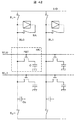
<製造方法の例示>
図42は、実施例1のDRAMの等価回路図である。等価回路自体は通例のものであるので詳細説明は省略するが、その概要は次の通りである。DRAMアレーは、基本的に、マトリクス状に配置された複数のワード線WL(WL0、WL1,・・・)と複数のビット線BL(BL0、BL1、・・・)およびこれらの交点に配置された複数のメモリセル(MC)により構成されている。1個のメモリセルは、1個のキャパシタCとこれに直列に接続された1個のメモリセル選択用のFETとで構成されている。メモリセル選択用のFETのソース及びドレインの一方は、キャパシタCと電気的に接続され、他方はビット線BLと電気的に接続されている。ワード線WLの一端は、ワードドライバ(図示されていない)に接続され、ビット線BLの一端は、センスアンプSAに接続されている。尚、I/Oは共通データ出力線、Coはデータ線寄生容量、S1は列選択スイッチ、S2はプリチャージスイッチである。
<Example of production method>
FIG. 42 is an equivalent circuit diagram of the DRAM of the first embodiment. Since the equivalent circuit itself is customary, detailed description thereof is omitted, but the outline thereof is as follows. The DRAM array is basically arranged at a plurality of word lines WL (WL0, WL1,...) And a plurality of bit lines BL (BL0, BL1,...) Arranged in a matrix and their intersections. The memory cell is composed of a plurality of memory cells (MC). One memory cell includes one capacitor C and one memory cell selection FET connected in series with the capacitor C. One of the source and drain of the memory cell selection FET is electrically connected to the capacitor C, and the other is electrically connected to the bit line BL. One end of the word line WL is connected to a word driver (not shown), and one end of the bit line BL is connected to the sense amplifier SA. Note that I / O is a common data output line, Co is a data line parasitic capacitance, S1 is a column selection switch, and S2 is a precharge switch.
本発明によるキャパシタを有するDRAMメモリキャパシタの製造方法を説明する。尚、本例では、情報蓄積用キャパシタは、絶縁膜の孔内の内面を、前記第2の電極、及び前記第2の電極上に成膜されたキャパシタ用絶縁膜、及び前記キャパシタ用絶縁膜上に成膜されたキャップ層絶縁膜、及び前記キャップ層絶縁膜上に成膜された第1の電極が形成された例である。 A method of manufacturing a DRAM memory capacitor having a capacitor according to the present invention will be described. In this example, the information storage capacitor has the inner surface in the hole of the insulating film, the second electrode, the capacitor insulating film formed on the second electrode, and the capacitor insulating film. This is an example in which a cap layer insulating film formed thereon and a first electrode formed on the cap layer insulating film are formed.
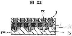
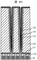
通例の方法で形成されたメモリセル選択トランジスタの上にビット線1を形成し、又、選択トランジスタとキャパシタとの電気的接続を行うポリシリコンプラグ2を形成する。図22が、このメモリの主要部の断面図である。図22中、符号aはトランジスタの拡散層を示す。拡散層aはシリコン基板30に通例の方法によりドーパントをインプラントして形成し、n型もしくはp型とする。また、図中、符号bに示すのはアイソレーションであり,隣接するトランジスタ同士の電気的分離を行なうものである。図中、符号20は絶縁膜を示す。尚、本例での図面は、メモリ部のトタンジスタに接続されるメモリ容量部の構造に関する発明であるので、この部分のみ図示し、半導体基板上に形成される半導体素子部については、以下の図面では、図示及び詳細説明は省略する。
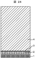
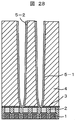
A
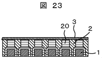
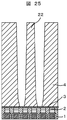
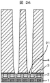
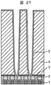
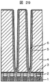
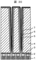
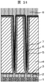
この上に、図23に示すように膜厚100nm程度の窒化シリコン膜3を化学気相成長法によって堆積する。このシリコン窒化膜は、以下の加工の際のエッチングストッパとして機能する。次に、図24に示すように、窒化シリコン膜3の上部にテトラエトキシシランを原料とする酸化シリコン膜4を形成した。この酸化シリコン膜4を、柱状酸化シリコン膜22に加工する。この状態の断面図が図25である。前記の加工は、フォトレジスト膜、ポリシリコン、タングステン、またはカーボン等、酸化シリコン膜とのエッチングの選択比が大きい材料をマスクとしてドライエッチング法を用いる。更に、窒化シリコン膜3のドライエッチングを続けて行い、図26に示すようにポリシリコンプラグ2の上部に下部電極用の溝21を形成した。更に、図27に示すように、下部電極材料として窒化チタン膜5を化学気相成長法または原子層成長法により35nm堆積する。下部電極材料はチタン、窒化タンタル、タンタル、窒化タングステン、タングステン、リンをドーピングしたポリシリコン、金、銀、銅、白金、など、酸化ハフニウム等の絶縁膜と積層した場合に急峻な界面を形成する材料であれば適用可能である。次に、図28に示すようなフォトレジスト膜を用いた通例のエッチバック技術によって、この窒化チタン膜5を各ビット毎5−1、5−2に分離する。尚、装置間搬送の際に、窒化チタン5表面に酸化チタンが2nm程度形成する。この酸化チタンは、例えばフッ化水素酸などを用いてウエットエッチングして除去する。続けて、図29に示すように絶縁膜として化学気相成長法または原子層成長法により酸化ハフニウム6を成膜する。その際、原子層成長法で成膜する場合の原料は、TEMAH(テトラ・エチル・メチル・アミド・ハフニウム)とオゾンを用いる。同絶縁膜は、酸化ジルコニウムでも良い。この酸化ハフニウム膜は、キャパシタの絶縁膜である。次に、図30に示すように、キャップ層絶縁膜として酸化タンタル7を化学気相成長法又は原子層成長法により2nm以上4nm以下成膜する。同キャップ層絶縁膜はニオブ酸化膜でも良い。次に、図31に示すように化学気相成長法または原子層成長法により上部電極向けのルテニウム8を原子層成長法により成膜する。上部電極材料は、酸化ルテニウムも適用可能である。
On this, a
<実施例2>
実施例1で示した結果は、キャパシタの上下関係を入れ替えても成立すると考えられる。つまり、下部電極にルテニウム、絶縁膜に二酸化ハフニウム、同ルテニウムと同二酸化ハフニウムは積層するとルテニウムが二酸化ハフニウム中に拡散するため、同界面にキャップ層絶縁膜として五酸化タンタルを挿入する。最後に上部電極として窒化チタンを形成する。同構造のキャパシタにおいても、実施例1で示したルテニウムが二酸化ハフニウム中に拡散してリーク電流密度のばらつきが増大するという問題点が生じるため、その解決方法として同界面に五酸化タンタルキャップ層絶縁膜を挿入し、同反応を抑制可能である。
<Example 2>
The result shown in Example 1 is considered to hold even if the upper and lower relations of the capacitors are switched. That is, when ruthenium is laminated on the lower electrode, hafnium dioxide is deposited on the insulating film, and ruthenium and hafnium dioxide are laminated, ruthenium diffuses into hafnium dioxide, so that tantalum pentoxide is inserted as a cap layer insulating film at the interface. Finally, titanium nitride is formed as the upper electrode. Even in the capacitor having the same structure, the ruthenium shown in the first embodiment is diffused into hafnium dioxide and the variation of the leakage current density is increased. A membrane can be inserted to suppress the reaction.
本実施例に即したキャパシタを有するDRAMメモリキャパシタの製造方法を説明する。尚、本例においても、図面は、メモリ部のトタンジスタに接続されるメモリ容量部の構造に関する発明であるので、この部分のみ図示し、半導体基板上に形成される半導体素子部については、図示及び詳細説明は省略する。 A method of manufacturing a DRAM memory capacitor having a capacitor according to the present embodiment will be described. In this example as well, since the drawings are inventions related to the structure of the memory capacity portion connected to the transistor of the memory portion, only this portion is shown, and the semiconductor element portion formed on the semiconductor substrate is illustrated and described. Detailed description is omitted.
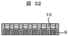
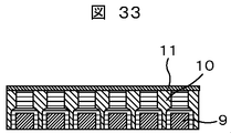
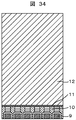
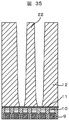
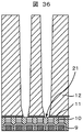
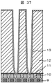
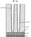
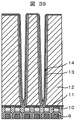
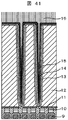
図32に示すように、通例の方法で形成されたメモリセル選択トランジスタの上にビット線9を形成し、また、選択トランジスタとキャパシタとの電気的接続を行なうポリシリコンプラグ10を形成する。この上に図33に示すように、膜厚100nm程度の窒化シリコン膜11を化学気相成長法によって堆積し、シリコン窒化膜を加工する際のエッチングストッパとする。次に、図34に示すように、窒化シリコン膜11の上部にテトラエトキシシランを原料とする酸化シリコン膜12を形成した。この酸化シリコン膜12を、図35に示すように柱状酸化シリコン22に加工する。この加工は、フォトレジスト膜、ポリシリコン、タングステン、またはカーボン等、酸化シリコン膜とのエッチングの選択比が大きい材料をマスクとしてドライエッチング法を用いた。更に、窒化シリコン膜11のドライエッチングを続けて行い、図36に示すようにポリシリコンプラグの上部に下部電極用の溝21を形成した。更に、図37に示すように、下部電極材料にルテニウム膜13を化学気相成長法又は原子層成長法により20nm堆積する。下部電極材料は特性が近い酸化ルテニウムも適用可能である。次に、図38に示すように、フォトレジスト膜を用いたエッチバック技術によって、このルテニウム膜13を各ビット毎13−1、13−2に分離する。尚、装置間搬送の際にルテニウム表面に酸化ルテニウムが1nm程度形成する。この酸化ルテニウムは、例えばフッ化水素酸などを用いてウエットエッチングして除去しても良い。続けて、図39に示すように、キャップ層絶縁膜14として酸化タンタルを化学気相成長法または原子層成長法により2nm以上5nm以下で成膜する。同キャップ層絶縁膜は、酸化ニオブでも良い。次に、図40に示すように絶縁膜として酸化ハフニウム15を化学気相成長法または原子層成長法により成膜する。原子層成長法により成膜する際の原料は、TEMAH(テトラ・エチル・メチル・アミド・ハフニウム)とオゾンを用いる。同絶縁膜は特性の近い酸化ジルコニウムでも良い。次に、図41に示すように上部電極向けの窒化チタン16を化学気相成長法又は原子層成長法により成膜する。上部電極材料は、チタン、窒化タンタル、タンタル、窒化タングステン、タングステン、リンをドーピングしたポリシリコン、金、銀、銅、白金など、絶縁膜と急峻な界面を形成する材料であれば適用可能である。
As shown in FIG. 32, a
本構造においても、実施例1と同等の装置特性を示した。 In this structure, the same device characteristics as those in Example 1 were shown.
1:ビット線、2:プラグ、3:窒化シリコン、4:酸化シリコン、5:下部電極(例えば、窒化チタン)、6:キャパシタ絶縁膜(例えば、酸化ハフニウム)、7:キャップ絶縁膜(例えば、酸化タンタル)、8:上部電極(例えば、ルテニウム)、9:ビット線、10:プラグ、11:窒化シリコン、12:酸化シリコン、13:下部電極(例えば、ルテニウム)、14:キャップ絶縁膜(例えば、酸化タンタル)、15:キャパシタ絶縁膜(例えば、酸化ハフニウム)、16:上部電極(例えば、窒化チタン)、20:絶縁膜、21:溝、22:柱状酸化シリコン膜:5−1、5−2:各ビット毎に分けられた窒化チタン膜、13−1、13−2:各ビット毎に分けられたルテニウム膜、30:シリコン基板、WL0、WL1:ワード線、BL0、BL2:ビット線、MC:メモリセル、C:キャパシタ、FET:電界効果型トランジスタ、C0:寄生容量、S1:列選択スイッチ、S2:プリチャージスイッチ。 1: bit line, 2: plug, 3: silicon nitride, 4: silicon oxide, 5: lower electrode (for example, titanium nitride), 6: capacitor insulating film (for example, hafnium oxide), 7: cap insulating film (for example, (Tantalum oxide), 8: upper electrode (for example, ruthenium), 9: bit line, 10: plug, 11: silicon nitride, 12: silicon oxide, 13: lower electrode (for example, ruthenium), 14: cap insulating film (for example, Tantalum oxide), 15: capacitor insulating film (for example, hafnium oxide), 16: upper electrode (for example, titanium nitride), 20: insulating film, 21: groove, 22: columnar silicon oxide film: 5-1, 5- 2: Titanium nitride film divided for each bit, 13-1, 13-2: Ruthenium film divided for each bit, 30: Silicon substrate, WL0, WL1: Word , BL0, BL2: bit lines, MC: memory cell, C: capacitor, FET: field effect transistor, C 0: parasitic capacitance, S1: column selection switches, S2: precharge switch.
Claims (8)
前記情報蓄積用キャパシタは、第2の電極、及び前記第2の電極上に成膜されたキャパシタ用絶縁膜、及び前記キャパシタ用絶縁膜上に成膜されたキャップ層絶縁膜、及び前記キャップ層絶縁膜上に成膜された第1の電極を有し、
前記第1の電極は、ルテニウム及び酸化ルテニウムから選ばれた少なくとも一者であり、
前記キャパシタ用絶縁膜は、酸化ハフニウム、イットリウムを添加した酸化ハフニウム、及び酸化ジルコニウムの群から選ばれた少なくとも一者であり、
前記キャップ層絶縁膜は、前記キャップ層絶縁膜は前記絶縁膜よりも誘電率の高い、酸化タンタル及び酸化ニオブから選ばれた少なくとも一者であり、
前記第2の電極は、窒化チタン、チタン、窒化タンタル、タンタル、窒化タングステン、タングステン、リンをドーピングしたポリシリコン、金、銀、銅、及びプラチナの群から選ばれた少なくとも一者であり、且つ
前記キャップ層絶縁膜が、連続膜を構成し且つ3nm以下の厚さであることを特徴とする半導体集積回路装置。 A plurality of word lines formed on a semiconductor substrate, a plurality of bit lines, a memory selection transistor provided at a predetermined intersection of the plurality of word lines and the plurality of bit lines, and the memory cell selection transistor A semiconductor integrated circuit device comprising a memory cell electrically connected in series and composed of an information storage capacitor formed on the semiconductor substrate,
The information storage capacitor includes a second electrode, a capacitor insulating film formed on the second electrode, a cap layer insulating film formed on the capacitor insulating film, and the cap layer A first electrode formed on the insulating film;
The first electrode is at least one selected from ruthenium and ruthenium oxide;
The capacitor insulating film is at least one selected from the group consisting of hafnium oxide, hafnium oxide added with yttrium, and zirconium oxide.
The cap layer insulating film is at least one selected from tantalum oxide and niobium oxide, wherein the cap layer insulating film has a dielectric constant higher than that of the insulating film.
The second electrode is at least one selected from the group consisting of titanium nitride, titanium, tantalum nitride, tantalum, tungsten nitride, tungsten, phosphorous doped polysilicon, gold, silver, copper, and platinum; and The semiconductor integrated circuit device, wherein the cap layer insulating film forms a continuous film and has a thickness of 3 nm or less.
前記情報蓄積用キャパシタは、第2の電極、及び前記第2の電極上に成膜されたキャップ層絶縁膜、及び前記キャップ層絶縁膜上に成膜されたキャパシタ用絶縁膜、及び前記キャップ層絶縁膜上に成膜された第1の電極を有し、
前記第1の電極は、ルテニウム及び酸化ルテニウムから選ばれた少なくとも一者であり、
前記キャパシタ用絶縁膜は、酸化ハフニウム、イットリウムを添加した酸化ハフニウム、及び酸化ジルコニウムの群から選ばれた少なくとも一者であり、
前記キャップ層絶縁膜は、前記キャップ層絶縁膜は前記キャパシタ用絶縁膜よりも誘電率の高い、酸化タンタル及び酸化ニオブから選ばれた少なくとも一者であり、
前記第2の電極は、窒化チタン、チタン、窒化タンタル、タンタル、窒化タングステン、タングステン、リンをドーピングしたポリシリコン、金、銀、銅、及びプラチナの群から選ばれた少なくとも一者であり、且つ
前記キャップ層絶縁膜が、連続膜を構成し且つ3nm以下の厚さであることを特徴とする半導体集積回路装置。 A plurality of word lines formed on a semiconductor substrate, a plurality of bit lines, a memory selection transistor provided at a predetermined intersection of the plurality of word lines and the plurality of bit lines, and the memory cell selection transistor A semiconductor integrated circuit device comprising a memory cell electrically connected in series and composed of an information storage capacitor formed on the semiconductor substrate,
The information storage capacitor includes a second electrode, a cap layer insulating film formed on the second electrode, a capacitor insulating film formed on the cap layer insulating film, and the cap layer A first electrode formed on the insulating film;
The first electrode is at least one selected from ruthenium and ruthenium oxide;
The capacitor insulating film is at least one selected from the group consisting of hafnium oxide, hafnium oxide added with yttrium, and zirconium oxide.
The cap layer insulating film is at least one selected from tantalum oxide and niobium oxide, wherein the cap layer insulating film has a higher dielectric constant than the capacitor insulating film,
The second electrode is at least one selected from the group consisting of titanium nitride, titanium, tantalum nitride, tantalum, tungsten nitride, tungsten, phosphorous doped polysilicon, gold, silver, copper, and platinum; and The semiconductor integrated circuit device, wherein the cap layer insulating film forms a continuous film and has a thickness of 3 nm or less.
Priority Applications (3)
| Application Number | Priority Date | Filing Date | Title |
|---|---|---|---|
| JP2006351721A JP2008166360A (en) | 2006-12-27 | 2006-12-27 | Semiconductor integrated circuit device |
| KR1020070104883A KR20080061250A (en) | 2006-12-27 | 2007-10-18 | Semiconductor integrated circuit device |
| US11/940,667 US20080157157A1 (en) | 2006-12-27 | 2007-11-15 | Semiconductor integrated circuit device |
Applications Claiming Priority (1)
| Application Number | Priority Date | Filing Date | Title |
|---|---|---|---|
| JP2006351721A JP2008166360A (en) | 2006-12-27 | 2006-12-27 | Semiconductor integrated circuit device |
Publications (1)
| Publication Number | Publication Date |
|---|---|
| JP2008166360A true JP2008166360A (en) | 2008-07-17 |
Family
ID=39582586
Family Applications (1)
| Application Number | Title | Priority Date | Filing Date |
|---|---|---|---|
| JP2006351721A Pending JP2008166360A (en) | 2006-12-27 | 2006-12-27 | Semiconductor integrated circuit device |
Country Status (3)
| Country | Link |
|---|---|
| US (1) | US20080157157A1 (en) |
| JP (1) | JP2008166360A (en) |
| KR (1) | KR20080061250A (en) |
Families Citing this family (297)
| Publication number | Priority date | Publication date | Assignee | Title |
|---|---|---|---|---|
| US10378106B2 (en) | 2008-11-14 | 2019-08-13 | Asm Ip Holding B.V. | Method of forming insulation film by modified PEALD |
| US9394608B2 (en) | 2009-04-06 | 2016-07-19 | Asm America, Inc. | Semiconductor processing reactor and components thereof |
| US8802201B2 (en) | 2009-08-14 | 2014-08-12 | Asm America, Inc. | Systems and methods for thin-film deposition of metal oxides using excited nitrogen-oxygen species |
| US9312155B2 (en) | 2011-06-06 | 2016-04-12 | Asm Japan K.K. | High-throughput semiconductor-processing apparatus equipped with multiple dual-chamber modules |
| US10364496B2 (en) | 2011-06-27 | 2019-07-30 | Asm Ip Holding B.V. | Dual section module having shared and unshared mass flow controllers |
| US10854498B2 (en) | 2011-07-15 | 2020-12-01 | Asm Ip Holding B.V. | Wafer-supporting device and method for producing same |
| US20130023129A1 (en) | 2011-07-20 | 2013-01-24 | Asm America, Inc. | Pressure transmitter for a semiconductor processing environment |
| US9017481B1 (en) | 2011-10-28 | 2015-04-28 | Asm America, Inc. | Process feed management for semiconductor substrate processing |
| US9659799B2 (en) | 2012-08-28 | 2017-05-23 | Asm Ip Holding B.V. | Systems and methods for dynamic semiconductor process scheduling |
| US9021985B2 (en) | 2012-09-12 | 2015-05-05 | Asm Ip Holdings B.V. | Process gas management for an inductively-coupled plasma deposition reactor |
| US10714315B2 (en) | 2012-10-12 | 2020-07-14 | Asm Ip Holdings B.V. | Semiconductor reaction chamber showerhead |
| KR20140048654A (en) | 2012-10-16 | 2014-04-24 | 삼성전자주식회사 | Semiconductor device |
| US8871621B2 (en) * | 2012-12-20 | 2014-10-28 | Intermolecular, Inc. | Method of forming an asymmetric MIMCAP or a schottky device as a selector element for a cross-bar memory array |
| US20160376700A1 (en) | 2013-02-01 | 2016-12-29 | Asm Ip Holding B.V. | System for treatment of deposition reactor |
| US9589770B2 (en) | 2013-03-08 | 2017-03-07 | Asm Ip Holding B.V. | Method and systems for in-situ formation of intermediate reactive species |
| US9484191B2 (en) | 2013-03-08 | 2016-11-01 | Asm Ip Holding B.V. | Pulsed remote plasma method and system |
| US9240412B2 (en) | 2013-09-27 | 2016-01-19 | Asm Ip Holding B.V. | Semiconductor structure and device and methods of forming same using selective epitaxial process |
| US10683571B2 (en) | 2014-02-25 | 2020-06-16 | Asm Ip Holding B.V. | Gas supply manifold and method of supplying gases to chamber using same |
| US10167557B2 (en) | 2014-03-18 | 2019-01-01 | Asm Ip Holding B.V. | Gas distribution system, reactor including the system, and methods of using the same |
| US11015245B2 (en) | 2014-03-19 | 2021-05-25 | Asm Ip Holding B.V. | Gas-phase reactor and system having exhaust plenum and components thereof |
| US10858737B2 (en) | 2014-07-28 | 2020-12-08 | Asm Ip Holding B.V. | Showerhead assembly and components thereof |
| US9890456B2 (en) | 2014-08-21 | 2018-02-13 | Asm Ip Holding B.V. | Method and system for in situ formation of gas-phase compounds |
| US10941490B2 (en) | 2014-10-07 | 2021-03-09 | Asm Ip Holding B.V. | Multiple temperature range susceptor, assembly, reactor and system including the susceptor, and methods of using the same |
| US9657845B2 (en) | 2014-10-07 | 2017-05-23 | Asm Ip Holding B.V. | Variable conductance gas distribution apparatus and method |
| KR102263121B1 (en) | 2014-12-22 | 2021-06-09 | 에이에스엠 아이피 홀딩 비.브이. | Semiconductor device and manufacuring method thereof |
| US10529542B2 (en) | 2015-03-11 | 2020-01-07 | Asm Ip Holdings B.V. | Cross-flow reactor and method |
| US10276355B2 (en) | 2015-03-12 | 2019-04-30 | Asm Ip Holding B.V. | Multi-zone reactor, system including the reactor, and method of using the same |
| US10458018B2 (en) | 2015-06-26 | 2019-10-29 | Asm Ip Holding B.V. | Structures including metal carbide material, devices including the structures, and methods of forming same |
| US10600673B2 (en) | 2015-07-07 | 2020-03-24 | Asm Ip Holding B.V. | Magnetic susceptor to baseplate seal |
| US10083836B2 (en) | 2015-07-24 | 2018-09-25 | Asm Ip Holding B.V. | Formation of boron-doped titanium metal films with high work function |
| US9960072B2 (en) | 2015-09-29 | 2018-05-01 | Asm Ip Holding B.V. | Variable adjustment for precise matching of multiple chamber cavity housings |
| US10211308B2 (en) | 2015-10-21 | 2019-02-19 | Asm Ip Holding B.V. | NbMC layers |
| US10322384B2 (en) | 2015-11-09 | 2019-06-18 | Asm Ip Holding B.V. | Counter flow mixer for process chamber |
| KR102406971B1 (en) | 2015-12-24 | 2022-06-10 | 삼성전자주식회사 | Semiconductor devices including capacitors and methods of manufacturing the same |
| US11139308B2 (en) | 2015-12-29 | 2021-10-05 | Asm Ip Holding B.V. | Atomic layer deposition of III-V compounds to form V-NAND devices |
| US10529554B2 (en) | 2016-02-19 | 2020-01-07 | Asm Ip Holding B.V. | Method for forming silicon nitride film selectively on sidewalls or flat surfaces of trenches |
| US10468251B2 (en) | 2016-02-19 | 2019-11-05 | Asm Ip Holding B.V. | Method for forming spacers using silicon nitride film for spacer-defined multiple patterning |
| US10501866B2 (en) | 2016-03-09 | 2019-12-10 | Asm Ip Holding B.V. | Gas distribution apparatus for improved film uniformity in an epitaxial system |
| US10343920B2 (en) | 2016-03-18 | 2019-07-09 | Asm Ip Holding B.V. | Aligned carbon nanotubes |
| US9892913B2 (en) | 2016-03-24 | 2018-02-13 | Asm Ip Holding B.V. | Radial and thickness control via biased multi-port injection settings |
| US10190213B2 (en) | 2016-04-21 | 2019-01-29 | Asm Ip Holding B.V. | Deposition of metal borides |
| US10865475B2 (en) | 2016-04-21 | 2020-12-15 | Asm Ip Holding B.V. | Deposition of metal borides and silicides |
| US10032628B2 (en) | 2016-05-02 | 2018-07-24 | Asm Ip Holding B.V. | Source/drain performance through conformal solid state doping |
| US10367080B2 (en) | 2016-05-02 | 2019-07-30 | Asm Ip Holding B.V. | Method of forming a germanium oxynitride film |
| KR102592471B1 (en) | 2016-05-17 | 2023-10-20 | 에이에스엠 아이피 홀딩 비.브이. | Method of forming metal interconnection and method of fabricating semiconductor device using the same |
| US11453943B2 (en) | 2016-05-25 | 2022-09-27 | Asm Ip Holding B.V. | Method for forming carbon-containing silicon/metal oxide or nitride film by ALD using silicon precursor and hydrocarbon precursor |
| US10388509B2 (en) | 2016-06-28 | 2019-08-20 | Asm Ip Holding B.V. | Formation of epitaxial layers via dislocation filtering |
| US9859151B1 (en) | 2016-07-08 | 2018-01-02 | Asm Ip Holding B.V. | Selective film deposition method to form air gaps |
| US10612137B2 (en) | 2016-07-08 | 2020-04-07 | Asm Ip Holdings B.V. | Organic reactants for atomic layer deposition |
| US10714385B2 (en) | 2016-07-19 | 2020-07-14 | Asm Ip Holding B.V. | Selective deposition of tungsten |
| KR102354490B1 (en) | 2016-07-27 | 2022-01-21 | 에이에스엠 아이피 홀딩 비.브이. | Method of processing a substrate |
| US10395919B2 (en) | 2016-07-28 | 2019-08-27 | Asm Ip Holding B.V. | Method and apparatus for filling a gap |
| US9812320B1 (en) | 2016-07-28 | 2017-11-07 | Asm Ip Holding B.V. | Method and apparatus for filling a gap |
| KR102532607B1 (en) | 2016-07-28 | 2023-05-15 | 에이에스엠 아이피 홀딩 비.브이. | Substrate processing apparatus and method of operating the same |
| US9887082B1 (en) | 2016-07-28 | 2018-02-06 | Asm Ip Holding B.V. | Method and apparatus for filling a gap |
| US10410943B2 (en) | 2016-10-13 | 2019-09-10 | Asm Ip Holding B.V. | Method for passivating a surface of a semiconductor and related systems |
| US10643826B2 (en) | 2016-10-26 | 2020-05-05 | Asm Ip Holdings B.V. | Methods for thermally calibrating reaction chambers |
| US11532757B2 (en) | 2016-10-27 | 2022-12-20 | Asm Ip Holding B.V. | Deposition of charge trapping layers |
| US10643904B2 (en) | 2016-11-01 | 2020-05-05 | Asm Ip Holdings B.V. | Methods for forming a semiconductor device and related semiconductor device structures |
| US10435790B2 (en) | 2016-11-01 | 2019-10-08 | Asm Ip Holding B.V. | Method of subatmospheric plasma-enhanced ALD using capacitively coupled electrodes with narrow gap |
| US10229833B2 (en) | 2016-11-01 | 2019-03-12 | Asm Ip Holding B.V. | Methods for forming a transition metal nitride film on a substrate by atomic layer deposition and related semiconductor device structures |
| US10714350B2 (en) | 2016-11-01 | 2020-07-14 | ASM IP Holdings, B.V. | Methods for forming a transition metal niobium nitride film on a substrate by atomic layer deposition and related semiconductor device structures |
| US10134757B2 (en) | 2016-11-07 | 2018-11-20 | Asm Ip Holding B.V. | Method of processing a substrate and a device manufactured by using the method |
| KR102546317B1 (en) | 2016-11-15 | 2023-06-21 | 에이에스엠 아이피 홀딩 비.브이. | Gas supply unit and substrate processing apparatus including the same |
| US10340135B2 (en) | 2016-11-28 | 2019-07-02 | Asm Ip Holding B.V. | Method of topologically restricted plasma-enhanced cyclic deposition of silicon or metal nitride |
| KR20180068582A (en) | 2016-12-14 | 2018-06-22 | 에이에스엠 아이피 홀딩 비.브이. | Substrate processing apparatus |
| US11581186B2 (en) | 2016-12-15 | 2023-02-14 | Asm Ip Holding B.V. | Sequential infiltration synthesis apparatus |
| US11447861B2 (en) | 2016-12-15 | 2022-09-20 | Asm Ip Holding B.V. | Sequential infiltration synthesis apparatus and a method of forming a patterned structure |
| KR20180070971A (en) | 2016-12-19 | 2018-06-27 | 에이에스엠 아이피 홀딩 비.브이. | Substrate processing apparatus |
| US10269558B2 (en) | 2016-12-22 | 2019-04-23 | Asm Ip Holding B.V. | Method of forming a structure on a substrate |
| US10867788B2 (en) | 2016-12-28 | 2020-12-15 | Asm Ip Holding B.V. | Method of forming a structure on a substrate |
| US10655221B2 (en) | 2017-02-09 | 2020-05-19 | Asm Ip Holding B.V. | Method for depositing oxide film by thermal ALD and PEALD |
| US10468261B2 (en) | 2017-02-15 | 2019-11-05 | Asm Ip Holding B.V. | Methods for forming a metallic film on a substrate by cyclical deposition and related semiconductor device structures |
| US10283353B2 (en) | 2017-03-29 | 2019-05-07 | Asm Ip Holding B.V. | Method of reforming insulating film deposited on substrate with recess pattern |
| US10529563B2 (en) | 2017-03-29 | 2020-01-07 | Asm Ip Holdings B.V. | Method for forming doped metal oxide films on a substrate by cyclical deposition and related semiconductor device structures |
| KR102457289B1 (en) | 2017-04-25 | 2022-10-21 | 에이에스엠 아이피 홀딩 비.브이. | Method for depositing a thin film and manufacturing a semiconductor device |
| US10446393B2 (en) | 2017-05-08 | 2019-10-15 | Asm Ip Holding B.V. | Methods for forming silicon-containing epitaxial layers and related semiconductor device structures |
| US10770286B2 (en) | 2017-05-08 | 2020-09-08 | Asm Ip Holdings B.V. | Methods for selectively forming a silicon nitride film on a substrate and related semiconductor device structures |
| US10892156B2 (en) | 2017-05-08 | 2021-01-12 | Asm Ip Holding B.V. | Methods for forming a silicon nitride film on a substrate and related semiconductor device structures |
| US10504742B2 (en) | 2017-05-31 | 2019-12-10 | Asm Ip Holding B.V. | Method of atomic layer etching using hydrogen plasma |
| US10886123B2 (en) | 2017-06-02 | 2021-01-05 | Asm Ip Holding B.V. | Methods for forming low temperature semiconductor layers and related semiconductor device structures |
| US11306395B2 (en) | 2017-06-28 | 2022-04-19 | Asm Ip Holding B.V. | Methods for depositing a transition metal nitride film on a substrate by atomic layer deposition and related deposition apparatus |
| US10685834B2 (en) | 2017-07-05 | 2020-06-16 | Asm Ip Holdings B.V. | Methods for forming a silicon germanium tin layer and related semiconductor device structures |
| KR20190009245A (en) | 2017-07-18 | 2019-01-28 | 에이에스엠 아이피 홀딩 비.브이. | Methods for forming a semiconductor device structure and related semiconductor device structures |
| US11018002B2 (en) | 2017-07-19 | 2021-05-25 | Asm Ip Holding B.V. | Method for selectively depositing a Group IV semiconductor and related semiconductor device structures |
| US11374112B2 (en) | 2017-07-19 | 2022-06-28 | Asm Ip Holding B.V. | Method for depositing a group IV semiconductor and related semiconductor device structures |
| US10541333B2 (en) | 2017-07-19 | 2020-01-21 | Asm Ip Holding B.V. | Method for depositing a group IV semiconductor and related semiconductor device structures |
| US10590535B2 (en) | 2017-07-26 | 2020-03-17 | Asm Ip Holdings B.V. | Chemical treatment, deposition and/or infiltration apparatus and method for using the same |
| US10312055B2 (en) | 2017-07-26 | 2019-06-04 | Asm Ip Holding B.V. | Method of depositing film by PEALD using negative bias |
| US10605530B2 (en) | 2017-07-26 | 2020-03-31 | Asm Ip Holding B.V. | Assembly of a liner and a flange for a vertical furnace as well as the liner and the vertical furnace |
| US10692741B2 (en) | 2017-08-08 | 2020-06-23 | Asm Ip Holdings B.V. | Radiation shield |
| US10770336B2 (en) | 2017-08-08 | 2020-09-08 | Asm Ip Holding B.V. | Substrate lift mechanism and reactor including same |
| US11139191B2 (en) | 2017-08-09 | 2021-10-05 | Asm Ip Holding B.V. | Storage apparatus for storing cassettes for substrates and processing apparatus equipped therewith |
| US10249524B2 (en) | 2017-08-09 | 2019-04-02 | Asm Ip Holding B.V. | Cassette holder assembly for a substrate cassette and holding member for use in such assembly |
| US11769682B2 (en) | 2017-08-09 | 2023-09-26 | Asm Ip Holding B.V. | Storage apparatus for storing cassettes for substrates and processing apparatus equipped therewith |
| US20190057860A1 (en) * | 2017-08-18 | 2019-02-21 | Lam Research Corporation | Methods for improving performance in hafnium oxide-based ferroelectric material using plasma and/or thermal treatment |
| US10236177B1 (en) | 2017-08-22 | 2019-03-19 | ASM IP Holding B.V.. | Methods for depositing a doped germanium tin semiconductor and related semiconductor device structures |
| USD900036S1 (en) | 2017-08-24 | 2020-10-27 | Asm Ip Holding B.V. | Heater electrical connector and adapter |
| US11830730B2 (en) | 2017-08-29 | 2023-11-28 | Asm Ip Holding B.V. | Layer forming method and apparatus |
| US11056344B2 (en) | 2017-08-30 | 2021-07-06 | Asm Ip Holding B.V. | Layer forming method |
| KR102491945B1 (en) | 2017-08-30 | 2023-01-26 | 에이에스엠 아이피 홀딩 비.브이. | Substrate processing apparatus |
| US11295980B2 (en) | 2017-08-30 | 2022-04-05 | Asm Ip Holding B.V. | Methods for depositing a molybdenum metal film over a dielectric surface of a substrate by a cyclical deposition process and related semiconductor device structures |
| US10607895B2 (en) | 2017-09-18 | 2020-03-31 | Asm Ip Holdings B.V. | Method for forming a semiconductor device structure comprising a gate fill metal |
| KR102630301B1 (en) | 2017-09-21 | 2024-01-29 | 에이에스엠 아이피 홀딩 비.브이. | Method of sequential infiltration synthesis treatment of infiltrateable material and structures and devices formed using same |
| US10844484B2 (en) | 2017-09-22 | 2020-11-24 | Asm Ip Holding B.V. | Apparatus for dispensing a vapor phase reactant to a reaction chamber and related methods |
| US10658205B2 (en) | 2017-09-28 | 2020-05-19 | Asm Ip Holdings B.V. | Chemical dispensing apparatus and methods for dispensing a chemical to a reaction chamber |
| US10403504B2 (en) | 2017-10-05 | 2019-09-03 | Asm Ip Holding B.V. | Method for selectively depositing a metallic film on a substrate |
| US10319588B2 (en) | 2017-10-10 | 2019-06-11 | Asm Ip Holding B.V. | Method for depositing a metal chalcogenide on a substrate by cyclical deposition |
| US10923344B2 (en) | 2017-10-30 | 2021-02-16 | Asm Ip Holding B.V. | Methods for forming a semiconductor structure and related semiconductor structures |
| KR102443047B1 (en) | 2017-11-16 | 2022-09-14 | 에이에스엠 아이피 홀딩 비.브이. | Method of processing a substrate and a device manufactured by the same |
| US10910262B2 (en) | 2017-11-16 | 2021-02-02 | Asm Ip Holding B.V. | Method of selectively depositing a capping layer structure on a semiconductor device structure |
| US11022879B2 (en) | 2017-11-24 | 2021-06-01 | Asm Ip Holding B.V. | Method of forming an enhanced unexposed photoresist layer |
| KR102597978B1 (en) | 2017-11-27 | 2023-11-06 | 에이에스엠 아이피 홀딩 비.브이. | Storage device for storing wafer cassettes for use with batch furnaces |
| US11639811B2 (en) | 2017-11-27 | 2023-05-02 | Asm Ip Holding B.V. | Apparatus including a clean mini environment |
| US10290508B1 (en) | 2017-12-05 | 2019-05-14 | Asm Ip Holding B.V. | Method for forming vertical spacers for spacer-defined patterning |
| US10872771B2 (en) | 2018-01-16 | 2020-12-22 | Asm Ip Holding B. V. | Method for depositing a material film on a substrate within a reaction chamber by a cyclical deposition process and related device structures |
| US11482412B2 (en) | 2018-01-19 | 2022-10-25 | Asm Ip Holding B.V. | Method for depositing a gap-fill layer by plasma-assisted deposition |
| TW202325889A (en) | 2018-01-19 | 2023-07-01 | 荷蘭商Asm 智慧財產控股公司 | Deposition method |
| USD903477S1 (en) | 2018-01-24 | 2020-12-01 | Asm Ip Holdings B.V. | Metal clamp |
| US11018047B2 (en) | 2018-01-25 | 2021-05-25 | Asm Ip Holding B.V. | Hybrid lift pin |
| US10535516B2 (en) | 2018-02-01 | 2020-01-14 | Asm Ip Holdings B.V. | Method for depositing a semiconductor structure on a surface of a substrate and related semiconductor structures |
| USD880437S1 (en) | 2018-02-01 | 2020-04-07 | Asm Ip Holding B.V. | Gas supply plate for semiconductor manufacturing apparatus |
| US11081345B2 (en) | 2018-02-06 | 2021-08-03 | Asm Ip Holding B.V. | Method of post-deposition treatment for silicon oxide film |
| WO2019158960A1 (en) | 2018-02-14 | 2019-08-22 | Asm Ip Holding B.V. | A method for depositing a ruthenium-containing film on a substrate by a cyclical deposition process |
| US10896820B2 (en) | 2018-02-14 | 2021-01-19 | Asm Ip Holding B.V. | Method for depositing a ruthenium-containing film on a substrate by a cyclical deposition process |
| US10731249B2 (en) | 2018-02-15 | 2020-08-04 | Asm Ip Holding B.V. | Method of forming a transition metal containing film on a substrate by a cyclical deposition process, a method for supplying a transition metal halide compound to a reaction chamber, and related vapor deposition apparatus |
| KR102636427B1 (en) | 2018-02-20 | 2024-02-13 | 에이에스엠 아이피 홀딩 비.브이. | Substrate processing method and apparatus |
| US10658181B2 (en) | 2018-02-20 | 2020-05-19 | Asm Ip Holding B.V. | Method of spacer-defined direct patterning in semiconductor fabrication |
| US10975470B2 (en) | 2018-02-23 | 2021-04-13 | Asm Ip Holding B.V. | Apparatus for detecting or monitoring for a chemical precursor in a high temperature environment |
| US11473195B2 (en) | 2018-03-01 | 2022-10-18 | Asm Ip Holding B.V. | Semiconductor processing apparatus and a method for processing a substrate |
| US11629406B2 (en) | 2018-03-09 | 2023-04-18 | Asm Ip Holding B.V. | Semiconductor processing apparatus comprising one or more pyrometers for measuring a temperature of a substrate during transfer of the substrate |
| US11114283B2 (en) | 2018-03-16 | 2021-09-07 | Asm Ip Holding B.V. | Reactor, system including the reactor, and methods of manufacturing and using same |
| KR102646467B1 (en) | 2018-03-27 | 2024-03-11 | 에이에스엠 아이피 홀딩 비.브이. | Method of forming an electrode on a substrate and a semiconductor device structure including an electrode |
| US10510536B2 (en) | 2018-03-29 | 2019-12-17 | Asm Ip Holding B.V. | Method of depositing a co-doped polysilicon film on a surface of a substrate within a reaction chamber |
| US11088002B2 (en) | 2018-03-29 | 2021-08-10 | Asm Ip Holding B.V. | Substrate rack and a substrate processing system and method |
| US11230766B2 (en) | 2018-03-29 | 2022-01-25 | Asm Ip Holding B.V. | Substrate processing apparatus and method |
| KR102501472B1 (en) | 2018-03-30 | 2023-02-20 | 에이에스엠 아이피 홀딩 비.브이. | Substrate processing method |
| TWI811348B (en) | 2018-05-08 | 2023-08-11 | 荷蘭商Asm 智慧財產控股公司 | Methods for depositing an oxide film on a substrate by a cyclical deposition process and related device structures |
| TWI816783B (en) | 2018-05-11 | 2023-10-01 | 荷蘭商Asm 智慧財產控股公司 | Methods for forming a doped metal carbide film on a substrate and related semiconductor device structures |
| KR102596988B1 (en) | 2018-05-28 | 2023-10-31 | 에이에스엠 아이피 홀딩 비.브이. | Method of processing a substrate and a device manufactured by the same |
| US11718913B2 (en) | 2018-06-04 | 2023-08-08 | Asm Ip Holding B.V. | Gas distribution system and reactor system including same |
| US11270899B2 (en) | 2018-06-04 | 2022-03-08 | Asm Ip Holding B.V. | Wafer handling chamber with moisture reduction |
| US11286562B2 (en) | 2018-06-08 | 2022-03-29 | Asm Ip Holding B.V. | Gas-phase chemical reactor and method of using same |
| KR102568797B1 (en) | 2018-06-21 | 2023-08-21 | 에이에스엠 아이피 홀딩 비.브이. | Substrate processing system |
| US10797133B2 (en) | 2018-06-21 | 2020-10-06 | Asm Ip Holding B.V. | Method for depositing a phosphorus doped silicon arsenide film and related semiconductor device structures |
| CN112292477A (en) | 2018-06-27 | 2021-01-29 | Asm Ip私人控股有限公司 | Cyclic deposition methods for forming metal-containing materials and films and structures containing metal-containing materials |
| JP2021529254A (en) | 2018-06-27 | 2021-10-28 | エーエスエム・アイピー・ホールディング・ベー・フェー | Periodic deposition methods for forming metal-containing materials and films and structures containing metal-containing materials |
| US10612136B2 (en) | 2018-06-29 | 2020-04-07 | ASM IP Holding, B.V. | Temperature-controlled flange and reactor system including same |
| KR20200002519A (en) | 2018-06-29 | 2020-01-08 | 에이에스엠 아이피 홀딩 비.브이. | Method for depositing a thin film and manufacturing a semiconductor device |
| US10388513B1 (en) | 2018-07-03 | 2019-08-20 | Asm Ip Holding B.V. | Method for depositing silicon-free carbon-containing film as gap-fill layer by pulse plasma-assisted deposition |
| US10755922B2 (en) | 2018-07-03 | 2020-08-25 | Asm Ip Holding B.V. | Method for depositing silicon-free carbon-containing film as gap-fill layer by pulse plasma-assisted deposition |
| US10767789B2 (en) | 2018-07-16 | 2020-09-08 | Asm Ip Holding B.V. | Diaphragm valves, valve components, and methods for forming valve components |
| US10483099B1 (en) | 2018-07-26 | 2019-11-19 | Asm Ip Holding B.V. | Method for forming thermally stable organosilicon polymer film |
| US11053591B2 (en) | 2018-08-06 | 2021-07-06 | Asm Ip Holding B.V. | Multi-port gas injection system and reactor system including same |
| US10883175B2 (en) | 2018-08-09 | 2021-01-05 | Asm Ip Holding B.V. | Vertical furnace for processing substrates and a liner for use therein |
| US10829852B2 (en) | 2018-08-16 | 2020-11-10 | Asm Ip Holding B.V. | Gas distribution device for a wafer processing apparatus |
| US11430674B2 (en) | 2018-08-22 | 2022-08-30 | Asm Ip Holding B.V. | Sensor array, apparatus for dispensing a vapor phase reactant to a reaction chamber and related methods |
| KR20200030162A (en) | 2018-09-11 | 2020-03-20 | 에이에스엠 아이피 홀딩 비.브이. | Method for deposition of a thin film |
| US11024523B2 (en) | 2018-09-11 | 2021-06-01 | Asm Ip Holding B.V. | Substrate processing apparatus and method |
| US11049751B2 (en) | 2018-09-14 | 2021-06-29 | Asm Ip Holding B.V. | Cassette supply system to store and handle cassettes and processing apparatus equipped therewith |
| CN110970344A (en) | 2018-10-01 | 2020-04-07 | Asm Ip控股有限公司 | Substrate holding apparatus, system including the same, and method of using the same |
| US11232963B2 (en) | 2018-10-03 | 2022-01-25 | Asm Ip Holding B.V. | Substrate processing apparatus and method |
| KR102592699B1 (en) | 2018-10-08 | 2023-10-23 | 에이에스엠 아이피 홀딩 비.브이. | Substrate support unit and apparatuses for depositing thin film and processing the substrate including the same |
| US10847365B2 (en) | 2018-10-11 | 2020-11-24 | Asm Ip Holding B.V. | Method of forming conformal silicon carbide film by cyclic CVD |
| US10811256B2 (en) | 2018-10-16 | 2020-10-20 | Asm Ip Holding B.V. | Method for etching a carbon-containing feature |
| KR102605121B1 (en) | 2018-10-19 | 2023-11-23 | 에이에스엠 아이피 홀딩 비.브이. | Substrate processing apparatus and substrate processing method |
| KR102546322B1 (en) | 2018-10-19 | 2023-06-21 | 에이에스엠 아이피 홀딩 비.브이. | Substrate processing apparatus and substrate processing method |
| USD948463S1 (en) | 2018-10-24 | 2022-04-12 | Asm Ip Holding B.V. | Susceptor for semiconductor substrate supporting apparatus |
| US10381219B1 (en) | 2018-10-25 | 2019-08-13 | Asm Ip Holding B.V. | Methods for forming a silicon nitride film |
| US11087997B2 (en) | 2018-10-31 | 2021-08-10 | Asm Ip Holding B.V. | Substrate processing apparatus for processing substrates |
| KR20200051105A (en) | 2018-11-02 | 2020-05-13 | 에이에스엠 아이피 홀딩 비.브이. | Substrate support unit and substrate processing apparatus including the same |
| US11572620B2 (en) | 2018-11-06 | 2023-02-07 | Asm Ip Holding B.V. | Methods for selectively depositing an amorphous silicon film on a substrate |
| US11031242B2 (en) | 2018-11-07 | 2021-06-08 | Asm Ip Holding B.V. | Methods for depositing a boron doped silicon germanium film |
| US10847366B2 (en) | 2018-11-16 | 2020-11-24 | Asm Ip Holding B.V. | Methods for depositing a transition metal chalcogenide film on a substrate by a cyclical deposition process |
| US10818758B2 (en) | 2018-11-16 | 2020-10-27 | Asm Ip Holding B.V. | Methods for forming a metal silicate film on a substrate in a reaction chamber and related semiconductor device structures |
| US10559458B1 (en) | 2018-11-26 | 2020-02-11 | Asm Ip Holding B.V. | Method of forming oxynitride film |
| US11217444B2 (en) | 2018-11-30 | 2022-01-04 | Asm Ip Holding B.V. | Method for forming an ultraviolet radiation responsive metal oxide-containing film |
| KR102636428B1 (en) | 2018-12-04 | 2024-02-13 | 에이에스엠 아이피 홀딩 비.브이. | A method for cleaning a substrate processing apparatus |
| US11158513B2 (en) | 2018-12-13 | 2021-10-26 | Asm Ip Holding B.V. | Methods for forming a rhenium-containing film on a substrate by a cyclical deposition process and related semiconductor device structures |
| JP2020096183A (en) | 2018-12-14 | 2020-06-18 | エーエスエム・アイピー・ホールディング・ベー・フェー | Method of forming device structure using selective deposition of gallium nitride, and system for the same |
| TWI819180B (en) | 2019-01-17 | 2023-10-21 | 荷蘭商Asm 智慧財產控股公司 | Methods of forming a transition metal containing film on a substrate by a cyclical deposition process |
| KR20200091543A (en) | 2019-01-22 | 2020-07-31 | 에이에스엠 아이피 홀딩 비.브이. | Semiconductor processing device |
| CN111524788B (en) | 2019-02-01 | 2023-11-24 | Asm Ip私人控股有限公司 | Method for topologically selective film formation of silicon oxide |
| JP2020136677A (en) | 2019-02-20 | 2020-08-31 | エーエスエム・アイピー・ホールディング・ベー・フェー | Periodic accumulation method for filing concave part formed inside front surface of base material, and device |
| US11482533B2 (en) | 2019-02-20 | 2022-10-25 | Asm Ip Holding B.V. | Apparatus and methods for plug fill deposition in 3-D NAND applications |
| KR102638425B1 (en) | 2019-02-20 | 2024-02-21 | 에이에스엠 아이피 홀딩 비.브이. | Method and apparatus for filling a recess formed within a substrate surface |
| KR102626263B1 (en) | 2019-02-20 | 2024-01-16 | 에이에스엠 아이피 홀딩 비.브이. | Cyclical deposition method including treatment step and apparatus for same |
| JP2020133004A (en) | 2019-02-22 | 2020-08-31 | エーエスエム・アイピー・ホールディング・ベー・フェー | Base material processing apparatus and method for processing base material |
| KR20200108243A (en) | 2019-03-08 | 2020-09-17 | 에이에스엠 아이피 홀딩 비.브이. | Structure Including SiOC Layer and Method of Forming Same |
| KR20200108242A (en) | 2019-03-08 | 2020-09-17 | 에이에스엠 아이피 홀딩 비.브이. | Method for Selective Deposition of Silicon Nitride Layer and Structure Including Selectively-Deposited Silicon Nitride Layer |
| US11742198B2 (en) | 2019-03-08 | 2023-08-29 | Asm Ip Holding B.V. | Structure including SiOCN layer and method of forming same |
| US10627696B1 (en) | 2019-03-18 | 2020-04-21 | Psiwuantum, Corp. | Active photonic devices incorporating high dielectric constant materials |
| JP2020167398A (en) | 2019-03-28 | 2020-10-08 | エーエスエム・アイピー・ホールディング・ベー・フェー | Door opener and substrate processing apparatus provided therewith |
| KR20200116855A (en) | 2019-04-01 | 2020-10-13 | 에이에스엠 아이피 홀딩 비.브이. | Method of manufacturing semiconductor device |
| US11447864B2 (en) | 2019-04-19 | 2022-09-20 | Asm Ip Holding B.V. | Layer forming method and apparatus |
| KR20200125453A (en) | 2019-04-24 | 2020-11-04 | 에이에스엠 아이피 홀딩 비.브이. | Gas-phase reactor system and method of using same |
| KR20200130118A (en) | 2019-05-07 | 2020-11-18 | 에이에스엠 아이피 홀딩 비.브이. | Method for Reforming Amorphous Carbon Polymer Film |
| KR20200130121A (en) | 2019-05-07 | 2020-11-18 | 에이에스엠 아이피 홀딩 비.브이. | Chemical source vessel with dip tube |
| KR20200130652A (en) | 2019-05-10 | 2020-11-19 | 에이에스엠 아이피 홀딩 비.브이. | Method of depositing material onto a surface and structure formed according to the method |
| JP2020188255A (en) | 2019-05-16 | 2020-11-19 | エーエスエム アイピー ホールディング ビー.ブイ. | Wafer boat handling device, vertical batch furnace, and method |
| USD947913S1 (en) | 2019-05-17 | 2022-04-05 | Asm Ip Holding B.V. | Susceptor shaft |
| USD975665S1 (en) | 2019-05-17 | 2023-01-17 | Asm Ip Holding B.V. | Susceptor shaft |
| USD935572S1 (en) | 2019-05-24 | 2021-11-09 | Asm Ip Holding B.V. | Gas channel plate |
| USD922229S1 (en) | 2019-06-05 | 2021-06-15 | Asm Ip Holding B.V. | Device for controlling a temperature of a gas supply unit |
| KR20200141002A (en) | 2019-06-06 | 2020-12-17 | 에이에스엠 아이피 홀딩 비.브이. | Method of using a gas-phase reactor system including analyzing exhausted gas |
| KR20200143254A (en) | 2019-06-11 | 2020-12-23 | 에이에스엠 아이피 홀딩 비.브이. | Method of forming an electronic structure using an reforming gas, system for performing the method, and structure formed using the method |
| USD944946S1 (en) | 2019-06-14 | 2022-03-01 | Asm Ip Holding B.V. | Shower plate |
| US11256115B1 (en) | 2019-06-21 | 2022-02-22 | Psiquantum, Corp. | Active photonic devices with enhanced Pockels effect via isotope substitution |
| USD931978S1 (en) | 2019-06-27 | 2021-09-28 | Asm Ip Holding B.V. | Showerhead vacuum transport |
| KR20210005515A (en) | 2019-07-03 | 2021-01-14 | 에이에스엠 아이피 홀딩 비.브이. | Temperature control assembly for substrate processing apparatus and method of using same |
| JP2021015791A (en) | 2019-07-09 | 2021-02-12 | エーエスエム アイピー ホールディング ビー.ブイ. | Plasma device and substrate processing method using coaxial waveguide |
| CN112216646A (en) | 2019-07-10 | 2021-01-12 | Asm Ip私人控股有限公司 | Substrate supporting assembly and substrate processing device comprising same |
| KR20210010307A (en) | 2019-07-16 | 2021-01-27 | 에이에스엠 아이피 홀딩 비.브이. | Substrate processing apparatus |
| KR20210010816A (en) | 2019-07-17 | 2021-01-28 | 에이에스엠 아이피 홀딩 비.브이. | Radical assist ignition plasma system and method |
| KR20210010820A (en) | 2019-07-17 | 2021-01-28 | 에이에스엠 아이피 홀딩 비.브이. | Methods of forming silicon germanium structures |
| US11643724B2 (en) | 2019-07-18 | 2023-05-09 | Asm Ip Holding B.V. | Method of forming structures using a neutral beam |
| CN112242296A (en) | 2019-07-19 | 2021-01-19 | Asm Ip私人控股有限公司 | Method of forming topologically controlled amorphous carbon polymer films |
| TW202113936A (en) | 2019-07-29 | 2021-04-01 | 荷蘭商Asm Ip私人控股有限公司 | Methods for selective deposition utilizing n-type dopants and/or alternative dopants to achieve high dopant incorporation |
| CN112309900A (en) | 2019-07-30 | 2021-02-02 | Asm Ip私人控股有限公司 | Substrate processing apparatus |
| CN112309899A (en) | 2019-07-30 | 2021-02-02 | Asm Ip私人控股有限公司 | Substrate processing apparatus |
| US11227782B2 (en) | 2019-07-31 | 2022-01-18 | Asm Ip Holding B.V. | Vertical batch furnace assembly |
| US11587814B2 (en) | 2019-07-31 | 2023-02-21 | Asm Ip Holding B.V. | Vertical batch furnace assembly |
| US11587815B2 (en) | 2019-07-31 | 2023-02-21 | Asm Ip Holding B.V. | Vertical batch furnace assembly |
| CN112323048B (en) | 2019-08-05 | 2024-02-09 | Asm Ip私人控股有限公司 | Liquid level sensor for chemical source container |
| USD965044S1 (en) | 2019-08-19 | 2022-09-27 | Asm Ip Holding B.V. | Susceptor shaft |
| USD965524S1 (en) | 2019-08-19 | 2022-10-04 | Asm Ip Holding B.V. | Susceptor support |
| JP2021031769A (en) | 2019-08-21 | 2021-03-01 | エーエスエム アイピー ホールディング ビー.ブイ. | Production apparatus of mixed gas of film deposition raw material and film deposition apparatus |
| USD979506S1 (en) | 2019-08-22 | 2023-02-28 | Asm Ip Holding B.V. | Insulator |
| USD930782S1 (en) | 2019-08-22 | 2021-09-14 | Asm Ip Holding B.V. | Gas distributor |
| USD949319S1 (en) | 2019-08-22 | 2022-04-19 | Asm Ip Holding B.V. | Exhaust duct |
| USD940837S1 (en) | 2019-08-22 | 2022-01-11 | Asm Ip Holding B.V. | Electrode |
| KR20210024423A (en) | 2019-08-22 | 2021-03-05 | 에이에스엠 아이피 홀딩 비.브이. | Method for forming a structure with a hole |
| KR20210024420A (en) | 2019-08-23 | 2021-03-05 | 에이에스엠 아이피 홀딩 비.브이. | Method for depositing silicon oxide film having improved quality by peald using bis(diethylamino)silane |
| US11286558B2 (en) | 2019-08-23 | 2022-03-29 | Asm Ip Holding B.V. | Methods for depositing a molybdenum nitride film on a surface of a substrate by a cyclical deposition process and related semiconductor device structures including a molybdenum nitride film |
| KR20210029090A (en) | 2019-09-04 | 2021-03-15 | 에이에스엠 아이피 홀딩 비.브이. | Methods for selective deposition using a sacrificial capping layer |
| KR20210029663A (en) | 2019-09-05 | 2021-03-16 | 에이에스엠 아이피 홀딩 비.브이. | Substrate processing apparatus |
| US11562901B2 (en) | 2019-09-25 | 2023-01-24 | Asm Ip Holding B.V. | Substrate processing method |
| CN112593212B (en) | 2019-10-02 | 2023-12-22 | Asm Ip私人控股有限公司 | Method for forming topologically selective silicon oxide film by cyclic plasma enhanced deposition process |
| TW202129060A (en) | 2019-10-08 | 2021-08-01 | 荷蘭商Asm Ip控股公司 | Substrate processing device, and substrate processing method |
| TW202115273A (en) | 2019-10-10 | 2021-04-16 | 荷蘭商Asm Ip私人控股有限公司 | Method of forming a photoresist underlayer and structure including same |
| KR20210045930A (en) | 2019-10-16 | 2021-04-27 | 에이에스엠 아이피 홀딩 비.브이. | Method of Topology-Selective Film Formation of Silicon Oxide |
| US11637014B2 (en) | 2019-10-17 | 2023-04-25 | Asm Ip Holding B.V. | Methods for selective deposition of doped semiconductor material |
| KR20210047808A (en) | 2019-10-21 | 2021-04-30 | 에이에스엠 아이피 홀딩 비.브이. | Apparatus and methods for selectively etching films |
| US11646205B2 (en) | 2019-10-29 | 2023-05-09 | Asm Ip Holding B.V. | Methods of selectively forming n-type doped material on a surface, systems for selectively forming n-type doped material, and structures formed using same |
| KR20210054983A (en) | 2019-11-05 | 2021-05-14 | 에이에스엠 아이피 홀딩 비.브이. | Structures with doped semiconductor layers and methods and systems for forming same |
| US11501968B2 (en) | 2019-11-15 | 2022-11-15 | Asm Ip Holding B.V. | Method for providing a semiconductor device with silicon filled gaps |
| KR20210062561A (en) | 2019-11-20 | 2021-05-31 | 에이에스엠 아이피 홀딩 비.브이. | Method of depositing carbon-containing material on a surface of a substrate, structure formed using the method, and system for forming the structure |
| CN112951697A (en) | 2019-11-26 | 2021-06-11 | Asm Ip私人控股有限公司 | Substrate processing apparatus |
| US11450529B2 (en) | 2019-11-26 | 2022-09-20 | Asm Ip Holding B.V. | Methods for selectively forming a target film on a substrate comprising a first dielectric surface and a second metallic surface |
| CN112885692A (en) | 2019-11-29 | 2021-06-01 | Asm Ip私人控股有限公司 | Substrate processing apparatus |
| CN112885693A (en) | 2019-11-29 | 2021-06-01 | Asm Ip私人控股有限公司 | Substrate processing apparatus |
| JP2021090042A (en) | 2019-12-02 | 2021-06-10 | エーエスエム アイピー ホールディング ビー.ブイ. | Substrate processing apparatus and substrate processing method |
| KR20210070898A (en) | 2019-12-04 | 2021-06-15 | 에이에스엠 아이피 홀딩 비.브이. | Substrate processing apparatus |
| JP2021097227A (en) | 2019-12-17 | 2021-06-24 | エーエスエム・アイピー・ホールディング・ベー・フェー | Method of forming vanadium nitride layer and structure including vanadium nitride layer |
| US11527403B2 (en) | 2019-12-19 | 2022-12-13 | Asm Ip Holding B.V. | Methods for filling a gap feature on a substrate surface and related semiconductor structures |
| JP2021109175A (en) | 2020-01-06 | 2021-08-02 | エーエスエム・アイピー・ホールディング・ベー・フェー | Gas supply assembly, components thereof, and reactor system including the same |
| KR20210095050A (en) | 2020-01-20 | 2021-07-30 | 에이에스엠 아이피 홀딩 비.브이. | Method of forming thin film and method of modifying surface of thin film |
| TW202130846A (en) | 2020-02-03 | 2021-08-16 | 荷蘭商Asm Ip私人控股有限公司 | Method of forming structures including a vanadium or indium layer |
| TW202146882A (en) | 2020-02-04 | 2021-12-16 | 荷蘭商Asm Ip私人控股有限公司 | Method of verifying an article, apparatus for verifying an article, and system for verifying a reaction chamber |
| US11776846B2 (en) | 2020-02-07 | 2023-10-03 | Asm Ip Holding B.V. | Methods for depositing gap filling fluids and related systems and devices |
| US11781243B2 (en) | 2020-02-17 | 2023-10-10 | Asm Ip Holding B.V. | Method for depositing low temperature phosphorous-doped silicon |
| TW202203344A (en) | 2020-02-28 | 2022-01-16 | 荷蘭商Asm Ip控股公司 | System dedicated for parts cleaning |
| US11876356B2 (en) | 2020-03-11 | 2024-01-16 | Asm Ip Holding B.V. | Lockout tagout assembly and system and method of using same |
| KR20210116240A (en) | 2020-03-11 | 2021-09-27 | 에이에스엠 아이피 홀딩 비.브이. | Substrate handling device with adjustable joints |
| CN113394086A (en) | 2020-03-12 | 2021-09-14 | Asm Ip私人控股有限公司 | Method for producing a layer structure having a target topological profile |
| KR20210124042A (en) | 2020-04-02 | 2021-10-14 | 에이에스엠 아이피 홀딩 비.브이. | Thin film forming method |
| TW202146689A (en) | 2020-04-03 | 2021-12-16 | 荷蘭商Asm Ip控股公司 | Method for forming barrier layer and method for manufacturing semiconductor device |
| TW202145344A (en) | 2020-04-08 | 2021-12-01 | 荷蘭商Asm Ip私人控股有限公司 | Apparatus and methods for selectively etching silcon oxide films |
| US11821078B2 (en) | 2020-04-15 | 2023-11-21 | Asm Ip Holding B.V. | Method for forming precoat film and method for forming silicon-containing film |
| KR20210132600A (en) | 2020-04-24 | 2021-11-04 | 에이에스엠 아이피 홀딩 비.브이. | Methods and systems for depositing a layer comprising vanadium, nitrogen, and a further element |
| TW202146831A (en) | 2020-04-24 | 2021-12-16 | 荷蘭商Asm Ip私人控股有限公司 | Vertical batch furnace assembly, and method for cooling vertical batch furnace |
| CN113555279A (en) | 2020-04-24 | 2021-10-26 | Asm Ip私人控股有限公司 | Method of forming vanadium nitride-containing layers and structures including the same |
| KR20210134226A (en) | 2020-04-29 | 2021-11-09 | 에이에스엠 아이피 홀딩 비.브이. | Solid source precursor vessel |
| KR20210134869A (en) | 2020-05-01 | 2021-11-11 | 에이에스엠 아이피 홀딩 비.브이. | Fast FOUP swapping with a FOUP handler |
| KR20210141379A (en) | 2020-05-13 | 2021-11-23 | 에이에스엠 아이피 홀딩 비.브이. | Laser alignment fixture for a reactor system |
| TW202147383A (en) | 2020-05-19 | 2021-12-16 | 荷蘭商Asm Ip私人控股有限公司 | Substrate processing apparatus |
| KR20210145078A (en) | 2020-05-21 | 2021-12-01 | 에이에스엠 아이피 홀딩 비.브이. | Structures including multiple carbon layers and methods of forming and using same |
| KR20210145080A (en) | 2020-05-22 | 2021-12-01 | 에이에스엠 아이피 홀딩 비.브이. | Apparatus for depositing thin films using hydrogen peroxide |
| TW202201602A (en) | 2020-05-29 | 2022-01-01 | 荷蘭商Asm Ip私人控股有限公司 | Substrate processing device |
| TW202218133A (en) | 2020-06-24 | 2022-05-01 | 荷蘭商Asm Ip私人控股有限公司 | Method for forming a layer provided with silicon |
| TW202217953A (en) | 2020-06-30 | 2022-05-01 | 荷蘭商Asm Ip私人控股有限公司 | Substrate processing method |
| KR20220010438A (en) | 2020-07-17 | 2022-01-25 | 에이에스엠 아이피 홀딩 비.브이. | Structures and methods for use in photolithography |
| TW202204662A (en) | 2020-07-20 | 2022-02-01 | 荷蘭商Asm Ip私人控股有限公司 | Method and system for depositing molybdenum layers |
| TW202212623A (en) | 2020-08-26 | 2022-04-01 | 荷蘭商Asm Ip私人控股有限公司 | Method of forming metal silicon oxide layer and metal silicon oxynitride layer, semiconductor structure, and system |
| USD990534S1 (en) | 2020-09-11 | 2023-06-27 | Asm Ip Holding B.V. | Weighted lift pin |
| USD1012873S1 (en) | 2020-09-24 | 2024-01-30 | Asm Ip Holding B.V. | Electrode for semiconductor processing apparatus |
| TW202229613A (en) | 2020-10-14 | 2022-08-01 | 荷蘭商Asm Ip私人控股有限公司 | Method of depositing material on stepped structure |
| TW202217037A (en) | 2020-10-22 | 2022-05-01 | 荷蘭商Asm Ip私人控股有限公司 | Method of depositing vanadium metal, structure, device and a deposition assembly |
| TW202223136A (en) | 2020-10-28 | 2022-06-16 | 荷蘭商Asm Ip私人控股有限公司 | Method for forming layer on substrate, and semiconductor processing system |
| KR20220076343A (en) | 2020-11-30 | 2022-06-08 | 에이에스엠 아이피 홀딩 비.브이. | an injector configured for arrangement within a reaction chamber of a substrate processing apparatus |
| US11946137B2 (en) | 2020-12-16 | 2024-04-02 | Asm Ip Holding B.V. | Runout and wobble measurement fixtures |
| TW202231903A (en) | 2020-12-22 | 2022-08-16 | 荷蘭商Asm Ip私人控股有限公司 | Transition metal deposition method, transition metal layer, and deposition assembly for depositing transition metal on substrate |
| USD1023959S1 (en) | 2021-05-11 | 2024-04-23 | Asm Ip Holding B.V. | Electrode for substrate processing apparatus |
| USD980813S1 (en) | 2021-05-11 | 2023-03-14 | Asm Ip Holding B.V. | Gas flow control plate for substrate processing apparatus |
| USD980814S1 (en) | 2021-05-11 | 2023-03-14 | Asm Ip Holding B.V. | Gas distributor for substrate processing apparatus |
| USD981973S1 (en) | 2021-05-11 | 2023-03-28 | Asm Ip Holding B.V. | Reactor wall for substrate processing apparatus |
| USD990441S1 (en) | 2021-09-07 | 2023-06-27 | Asm Ip Holding B.V. | Gas flow control plate |
Family Cites Families (3)
| Publication number | Priority date | Publication date | Assignee | Title |
|---|---|---|---|---|
| KR101001741B1 (en) * | 2003-08-18 | 2010-12-15 | 삼성전자주식회사 | Capacitor of semiconductor device, method of manufacturing the same and memory device having the same |
| KR100541551B1 (en) * | 2003-09-19 | 2006-01-10 | 삼성전자주식회사 | Analog capacitor having at least 3 layers of high-k dielectric layers and method of fabricating the same |
| DE102004043857B3 (en) * | 2004-09-10 | 2006-03-30 | Infineon Technologies Ag | DRAM cell pair and DRAM memory cell array with stack and trench memory cells, and method of fabricating a DRAM memory cell array |
-
2006
- 2006-12-27 JP JP2006351721A patent/JP2008166360A/en active Pending
-
2007
- 2007-10-18 KR KR1020070104883A patent/KR20080061250A/en not_active Application Discontinuation
- 2007-11-15 US US11/940,667 patent/US20080157157A1/en not_active Abandoned
Also Published As
| Publication number | Publication date |
|---|---|
| US20080157157A1 (en) | 2008-07-03 |
| KR20080061250A (en) | 2008-07-02 |
Similar Documents
| Publication | Publication Date | Title |
|---|---|---|
| JP2008166360A (en) | Semiconductor integrated circuit device | |
| US20200227423A1 (en) | Ferroelectric Devices and Methods of Forming Ferroelectric Devices | |
| US7859081B2 (en) | Capacitor, method of increasing a capacitance area of same, and system containing same | |
| US9178006B2 (en) | Methods to improve electrical performance of ZrO2 based high-K dielectric materials for DRAM applications | |
| US10685964B2 (en) | Semiconductor structure for preventing row hammering issue in DRAM cell and method for manufacturing the same | |
| US6664157B2 (en) | Semiconductor integrated circuit device and the method of producing the same | |
| US11769816B2 (en) | Ferroelectric assemblies and methods of forming ferroelectric assemblies | |
| US6235579B1 (en) | Method for manufacturing stacked capacitor | |
| US9006906B2 (en) | DRAM cell based on conductive nanochannel plate | |
| JP2006060230A (en) | Three-dimensional semiconductor capacitor and its manufacturing method | |
| US11488958B2 (en) | Semiconductor device electrodes including fluorine | |
| CN113078115A (en) | Semiconductor structure and forming method thereof | |
| CN112750950A (en) | Semiconductor device with a plurality of semiconductor chips | |
| CN115148705A (en) | Semiconductor structure and preparation method thereof | |
| US11411071B1 (en) | Capacitor array structure and method for manufacturing a capacitor array structure, and semiconductor memory device | |
| US20230232607A1 (en) | Semiconductor device structure and method making the same | |
| US20220336737A1 (en) | Multi-doped data storage structure configured to improve resistive memory cell performance | |
| Schroeder et al. | Materials for DRAM memory cell applications | |
| US20220406735A1 (en) | Semiconductor device and method for manufacturing same | |
| US20240032273A1 (en) | Memory device and manufacturing method thereof | |
| US20240098976A1 (en) | Semiconductor device and method for manufacturing semiconductor device | |
| US20240038265A1 (en) | Spacer film scheme form polarization improvement | |
| US20230070343A1 (en) | Semiconductor device and method for forming the same | |
| US20220399490A1 (en) | Memory device and method of manufacturing the same | |
| TW427003B (en) | Manufacturing method of crown type DRAM capacitor |