JP2008046902A - Information processing system, information processing board, cache tag, and method for updating snoop tag - Google Patents
Information processing system, information processing board, cache tag, and method for updating snoop tag Download PDFInfo
- Publication number
- JP2008046902A JP2008046902A JP2006222439A JP2006222439A JP2008046902A JP 2008046902 A JP2008046902 A JP 2008046902A JP 2006222439 A JP2006222439 A JP 2006222439A JP 2006222439 A JP2006222439 A JP 2006222439A JP 2008046902 A JP2008046902 A JP 2008046902A
- Authority
- JP
- Japan
- Prior art keywords
- tag
- cache
- processor
- snoop
- way
- Prior art date
- Legal status (The legal status is an assumption and is not a legal conclusion. Google has not performed a legal analysis and makes no representation as to the accuracy of the status listed.)
- Pending
Links
Images


Classifications
-
- G—PHYSICS
- G06—COMPUTING; CALCULATING OR COUNTING
- G06F—ELECTRIC DIGITAL DATA PROCESSING
- G06F12/00—Accessing, addressing or allocating within memory systems or architectures
- G06F12/02—Addressing or allocation; Relocation
- G06F12/08—Addressing or allocation; Relocation in hierarchically structured memory systems, e.g. virtual memory systems
- G06F12/0802—Addressing of a memory level in which the access to the desired data or data block requires associative addressing means, e.g. caches
- G06F12/0806—Multiuser, multiprocessor or multiprocessing cache systems
- G06F12/0815—Cache consistency protocols
- G06F12/0817—Cache consistency protocols using directory methods
- G06F12/0822—Copy directories
-
- G—PHYSICS
- G06—COMPUTING; CALCULATING OR COUNTING
- G06F—ELECTRIC DIGITAL DATA PROCESSING
- G06F9/00—Arrangements for program control, e.g. control units
- G06F9/06—Arrangements for program control, e.g. control units using stored programs, i.e. using an internal store of processing equipment to receive or retain programs
- G06F9/46—Multiprogramming arrangements
-
- G—PHYSICS
- G06—COMPUTING; CALCULATING OR COUNTING
- G06F—ELECTRIC DIGITAL DATA PROCESSING
- G06F12/00—Accessing, addressing or allocating within memory systems or architectures
-
- G—PHYSICS
- G06—COMPUTING; CALCULATING OR COUNTING
- G06F—ELECTRIC DIGITAL DATA PROCESSING
- G06F12/00—Accessing, addressing or allocating within memory systems or architectures
- G06F12/02—Addressing or allocation; Relocation
- G06F12/08—Addressing or allocation; Relocation in hierarchically structured memory systems, e.g. virtual memory systems
- G06F12/0802—Addressing of a memory level in which the access to the desired data or data block requires associative addressing means, e.g. caches
- G06F12/0806—Multiuser, multiprocessor or multiprocessing cache systems
- G06F12/0815—Cache consistency protocols
- G06F12/0831—Cache consistency protocols using a bus scheme, e.g. with bus monitoring or watching means
Landscapes
- Engineering & Computer Science (AREA)
- Theoretical Computer Science (AREA)
- Physics & Mathematics (AREA)
- General Engineering & Computer Science (AREA)
- General Physics & Mathematics (AREA)
- Software Systems (AREA)
- Memory System Of A Hierarchy Structure (AREA)
Abstract
Description
本発明は、プロセッサバス上に複数のCPUコアを持ち、CPU内キャッシュのコピーであるスヌープタグをシステムコントローラが持つシステムのタグ構成に関する。 The present invention relates to a tag configuration of a system having a plurality of CPU cores on a processor bus and a system controller having a snoop tag that is a copy of a cache in the CPU.
一般に、CPUよりも低速な主記憶装置へのアクセスのスループットを向上させる手段として、キャッシュメモリが使用されている。キャッシュメモリは、通常、CPUと主記憶装置との間に配置され、CPU内に設けられることが一般的である。 In general, a cache memory is used as means for improving the throughput of access to a main storage device that is slower than the CPU. The cache memory is generally arranged between the CPU and the main storage device and is generally provided in the CPU.
キャッシュメモリと主記憶装置で使用される記憶装置(外部メモリ)とを比較すると、キャッシュメモリの方がアクセス速度は高速であるが、記憶容量が小さい。したがって、キャッシュメモリに格納されるデータは、外部メモリに展開された全データの一部である。 Comparing the cache memory and the storage device (external memory) used in the main storage device, the cache memory has a higher access speed but a smaller storage capacity. Therefore, the data stored in the cache memory is a part of all the data expanded in the external memory.
キャッシュメモリに読み出し対象のデータが存在すれば、高速でそのデータを読み出すことができる。しかし、キャッシュメモリに読み出し対象のデータが存在しなければ、主記憶装置へアクセスして読み出し対象となるデータを読み出すことになり、読み出し速度は低下することになる。 If there is data to be read in the cache memory, the data can be read at high speed. However, if there is no data to be read in the cache memory, the main storage device is accessed to read the data to be read, and the reading speed is reduced.
キャッシュメモリは、通常、主記憶装置に保持されているデータの一部を格納するキャッシュ(データ領域。または、キャッシュデータという)と、キャッシュに格納されているデータのアドレスの一部(タグ)を格納するタグメモリ(タグ領域、またはキャッシュタグという)とで構成される。 A cache memory usually includes a cache (data area or cache data) for storing a part of data held in the main storage device, and a part (tag) of an address of data stored in the cache. It consists of a tag memory to store (referred to as a tag area or cache tag).
プロセッサは、実行に必要なデータがキャッシュに存在するか否かを、当該データのアドレスとタグメモリ中のタグとを比較することにより知る。必要なデータがキャッシュ 中に存在しない場合、当該データが主メモリからキャッシュにロードされ、当該データのアドレスの一部が新しいタグとしてタグメモリにロードされる。この新しいタグをタグメモリにロードするため、タグメモリから不要な、あるいは不要と思われるタグを追い出す必要がある。 The processor knows whether or not the data necessary for execution exists in the cache by comparing the address of the data with the tag in the tag memory. If the required data does not exist in the cache, the data is loaded from the main memory into the cache, and a part of the address of the data is loaded into the tag memory as a new tag. In order to load this new tag into the tag memory, it is necessary to eject unnecessary or unnecessary tags from the tag memory.
タグメモリは、複数のウェイ(WAY)からなる。新しいタグのロードに先立って追い出すタグを決定する(タグの更新を行う)ために、タグに予めLRU(Least Recently Used)情報が付加される。 The tag memory is composed of a plurality of ways (WAY). LRU (Least Recently Used) information is added to the tag in advance in order to determine a tag to be expelled prior to loading a new tag (to update the tag).
例えば、LRU情報生成回路は、どのタグを次に置き換えるべきかを示すLRU情報をタグの書き込み時に生成し、当該タグに対応させてタグメモリに書き込む。従って、タグメモリの読み出し/書き込みの単位である1ラインにはタグとそのLRU情報とが格納される。新しいタグをタグメモリにロードする時に、補充先ウェイ情報生成回路が当該タグをどのウェイに補充するかをタグの各々に付加されたLRU情報を用いて判定する。 For example, the LRU information generation circuit generates LRU information indicating which tag is to be replaced next when writing the tag, and writes it in the tag memory in association with the tag. Therefore, a tag and its LRU information are stored in one line which is a unit for reading / writing the tag memory. When a new tag is loaded into the tag memory, the replenishment destination way information generation circuit determines which way to replenish the tag using the LRU information added to each tag.
マッチ判定回路はプロセッサが必要とするデータのアドレス(の一部)とタグメモリに格納している所定のタグとの比較を行い、当該データがキャッシュ中に存在するか否かを判定する。 The match determination circuit compares (part of) the address of data required by the processor with a predetermined tag stored in the tag memory, and determines whether or not the data exists in the cache.
この判定の後、タグメモリから読み出されたタグ(のライン)は、再びタグメモリに書き込まれる。即ち、当該判定の後にタグの書き戻しサイクルが実行される。これは、タグの当該ラインのLRU情報をタグメモリに書き戻さなければ、LRU情報が当該判定の結果を反映した正しいLRU情報であるとは言えなくなるためである。そこで、当該ラインのヒット/ミスヒットの結果に基づいて、LRU情報生成回路が新たなLRU情報を生成してこれをタグメモリに格納する。これにより、LRU情報を用いた新たなタグの書き込みのLRU制御が行われる。 After this determination, the tag (line) read from the tag memory is written to the tag memory again. That is, a tag write-back cycle is executed after the determination. This is because it cannot be said that the LRU information is correct LRU information reflecting the result of the determination unless the LRU information of the line of the tag is written back to the tag memory. Therefore, based on the hit / miss hit result of the line, the LRU information generation circuit generates new LRU information and stores it in the tag memory. Thereby, LRU control of writing a new tag using the LRU information is performed.
図6は、一般的なマルチプロセッサ構成を備える情報処理システムの全体図(チップセット)を示す。同図において情報処理システムは、主としてシステムボード10、入出力制御ユニット15、データクロスバー17、アドレスクロスバー16から構成される。システムボード10は、システムコントローラ1、ファームウェアハブ11、CPU2、メモリコントローラ12、メモリ13、CPUバス6、ファームウェアハブバス7から構成される。
FIG. 6 shows an overall view (chip set) of an information processing system having a general multiprocessor configuration. In FIG. 1, the information processing system mainly includes a
CPUバス6は、システムコントローラ1とCPU2とを接続するものである。ファームウェアハブバス7は、システムコントローラ1とファームウェアバブ7とを接続するものである。データクロスバー17は、システムボード10間のデータを送受するバスである。アドレスクロスバー16は、システムボード10間のアドレスを送受するバスである。
The
システムコントローラ1は、CPU2−メモリ13間のデータの送受を制御するための装置である。ファームウェアハブ11には、ファームウェアが格納されている。メモリコントローラ12は、メモリ13の動作を制御するものである。
The
図7は、情報処理システムにおけるタグを示す。図7において、システムコントローラ1は、CPUバス6a,6b,6c,6dによりCPU2a,2b,2c,2dと接続されている。各CPU2(2a,2b,2c,2d)はそれぞれキャッシュメモリを備えている。各CPU2のキャッシュメモリはそれぞれ、キャッシュタグ3(3a,3b,3c,3d)とキャッシュデータ4(4a,4b,4c,4d)により構成される。
FIG. 7 shows tags in the information processing system. In FIG. 7, the
また、システムコントローラ1内には各キャッシュタグ3(3a,3b,3c,3d)に対応したスヌープタグ5(5a,5b,5c,5d)を備える。
システムコントローラ1は、例えばキャッシュミス発生時にCPU2aからリード要求があれば、そのリード要求の対象となるデータが他のスヌープタグ5b,5c,5dで保持されているかを確認する。そのリード要求の対象となるデータが他のスヌープタグ5b,5c,5dで保持されている場合、システムコントローラ1は、そのタグが保持されたスヌープタグ5からそのリード要求に対応するリプレース情報を取得して、CPU2aに渡す。しかし、いずれのスヌープタグ5にもそのリード要求の対象となるデータが保持されていなければ、システムコントローラ1は、主記憶装置よりそのリード要求に対応するリプレース情報を取得して、CPU2aに渡す。
Further, the
For example, if there is a read request from the
図8は、従来におけるタグの構成例である。同図におけるCPU2aに着目して説明する。CPU2a内のキャッシュタグ3aは、例えば4つのWAY(3a−0,3a−1,3a−2,3a−3)からなる。
FIG. 8 shows a configuration example of a conventional tag. Description will be made by paying attention to the
一方、キャッシュタグ3aに対応するシステムコントロール1のスヌープタグ5aも、同様に4つのWAY(5a−0,5a−1,5a−2,5a−3)からなる。
このように、従来の構成では、CPU2のキャッシュタグ3と、システムコントローラ1のスヌープタグ5のWAY数は同じである。このような場合には、次の事象が起こり得る。
On the other hand, the
Thus, in the conventional configuration, the number of WAYs of the
まず、CPU2からシステムコントローラ1へキャッシュミスによるリード要求が発行(6a−Aa)されたときに、キャッシュタグ3がFULL(すなわち、キャッシュタグを構成する全てのWAYが書き込み状態)である場合、CPU2はキャッシュタグ3を構成するいずれかのWAYからアドレスを追い出して、リード要求の対象となるデータのアドレスに置き換える(リプレース情報)。
First, when a read request due to a cache miss is issued from the
このようなシステムにおいては、どのWAYのアドレスを追い出すかのリプレース情報をCPU2からシステムコントローラ1に知らせる手段が無いか、またはそのような手段があっても確実にそのリプレース情報が通知されるとは限らない。
In such a system, there is no means for the
よって、そのリプレース情報をCPU2からシステムコントローラ1に知らせる手段が無いか、またはそのような手段があっても確実にその削除情報が通知されるとは限らないプロトコルを前提する方式を採用しているシステムでは、システムコントローラ1側でスヌープタグのリプレース対象を独自に決定している。
図9A及び図9Bは、従来におけるキャッシュミス発生時のタグの更新例を示す。CPU2a内キャッシュタグ3aを構成する4つのWAY(3a−0,3a−1,3a−2,3a−3)にはそれぞれ、アドレス(0,1,2,3)が格納されているとする(CPU2a内キャッシュタグ3aがFULLの状態)。
9A and 9B show an example of updating a tag when a cache miss occurs in the related art. Assume that addresses (0, 1, 2, 3) are stored in the four WAYs (3a-0, 3a-1, 3a-2, 3a-3) constituting the
まず、CPU2aにおいて、キャッシュミスによるリード要求が発生する。例えば、アドレス5についてのリード要求が発生する(ステップ101。以下、ステップを「S」と称する)。
First, a read request due to a cache miss occurs in the
そうすると、CPU2aは、例えばキャッシュタグ3aのWAY[3a−0]をリプレース対象に決定し、WAY[3a−0]に格納されているアドレス情報(アドレス0)を削除する(S102)。
Then, the
CPU2aは、S101で発生したアドレス情報(アドレス5)についてのリード要求をシステムコントローラ1に対して行う(S103)。
スヌープタグ5aの全てのWAYはアドレスが書き込まれているため(FULL状態)、いずれかのWAYをリプレース対象として削除する必要がある。
The
Since all WAYs of the
しかしながら、CPU2aからリプレース要求がないシステムにおいては、システムコントローラ1側で、スヌープタグのどのWAYについてのアドレスを置換対象とするかを勝手に決定せざるを得ない。
However, in a system in which there is no replacement request from the
そこで、システムコントローラ1は、例えばリプレース対象としてWAY[5a−2]を決定し、そのWAY[5a−2]に格納されているアドレス情報(アドレス2)を削除する。
Therefore, the
リプレース対象となったWAY[5a−2]に格納されたアドレスは、CPU2a内のキャッシュタグ3aにおいてもリプレース対象となる。よって、システムコントローラ1は、リプレース対象となったアドレス(アドレス2)の削除をCPU2aへ要求する(Eviction要求)(S104)。
The address stored in the WAY [5a-2] that is the replacement target is also the replacement target in the
Eviction要求を受け取ったCPU2aは、そのコマンドを解析し、キャッシュタグ3aのWAY[3a−2]のアドレス情報(アドレス2)を削除する(S105)。
システムコントローラ1は、スヌープタグ5aのWAY[5a−2]を更新する(WAY[5a−2]にアドレス5が格納される)。そして、システムコントローラ1は、そのアドレス情報に対応するデータをCPU2aに送信する(S106)。
The
The
CPU2aは、システムコントローラ1からのデータを受信してキャッシュデータ4aに書き込むとともに、そのデータに対応するアドレスによりキャッシュタグ3aのWAY[3a−0]を更新する(S107)。
The
再度、CPU2aにおいて、キャッシュミスによるリード要求が発生する。例えば、アドレス6についてのリード要求が発生する(S108)。このとき、キャッシュタグ3(WAY[3a−2])には空きがあるので、S102で述べた削除処理は行われず、CPU2aはシステムコントローラ1へアドレス6についてのリード要求を行う(S109)。
Again, a read request due to a cache miss occurs in the
そうすると、スヌープタグ5aがFULLであるため、システムコントローラ1は、例えばWAY[5a−1]をリプレース対象に決定すると、そのWAY[5a−1]に格納されたアドレス情報(アドレス1)を削除する。
Then, since the snoop
リプレース対象となったWAY[5a−1]に格納されたアドレスは、キャッシュタグ3aにおいてもリプレース対象となる。よって、システムコントローラ1は、リプレース対象となったアドレス(アドレス1)の削除をCPU2aへ要求する(Eviction要求)(S110)。
The address stored in WAY [5a-1] that is the replacement target is also the replacement target in the
Eviction要求を受け取ったCPU2aは、そのコマンドを解析し、キャッシュタグ3aのWAY[3a−1]に格納されたアドレス情報(アドレス1)を削除する(S111)。
The
システムコントローラ1は、スヌープタグ5aのWAY[5a−1]を更新する(WAY[5a−1]にアドレス6が格納される)。そして、システムコントローラ1は、そのアドレスに対応するデータをCPU2aに送信する(S112)。
The
CPU2aは、システムコントローラ1からのデータを受信してキャッシュデータ4aに書き込むとともに、そのデータに対応するアドレスによりキャッシュタグ3aのWAY[3a−0]を更新する(S113)。
The
このように従来の構成では、CPU2とシステムコントローラ1のリプレース対象が必ずしも一致しないため、CPU2で余分なリプレースが生じてしまう。その結果、空きWAYの数も複数個生じることになる。そうすると、キャッシュミス率も増大することになる。
As described above, in the conventional configuration, the replacement target of the
上記の課題に鑑み、本発明では、CPUからシステムコントローラへどのWAYに格納された情報を追い出すかという情報が通知されない情報処理システムにおいて、CPU内のキャッシュタグの過剰なリプレースを抑制することにより、キャッシュミス率を減らし、性能低下を抑えることを目的とする。 In view of the above problems, in the present invention, in an information processing system in which information on which way stored information is driven out from the CPU to the system controller is not notified, by suppressing excessive replacement of the cache tag in the CPU, The purpose is to reduce the cache miss rate and suppress performance degradation.
本発明にかかる情報処理システムは、複数ウェイからなるキャッシュタグとキャッシュデータを含むキャッシュメモリを有し、外部から受け取った命令を実行及びデータを処理する1つ以上のプロセッサと、前記プロセッサからの読み出し要求に基づいて該プロセッサへ応答するプロセッサ制御装置であって、該各プロセッサのキャッシュタグに対応するタグ情報であるスヌープタグのウェイ数が前記プロセッサのキャッシュタグのウェイ数よりも多い該スヌープタグを有する該プロセッサ制御装置と、を備えることを特徴とする。 An information processing system according to the present invention has a cache memory including a plurality of ways of cache tags and cache data, and executes one or more processors that execute instructions received from outside and process data, and read from the processors A processor control device which responds to the processor based on a request, wherein the number of ways of the snoop tag which is tag information corresponding to the cache tag of each processor is greater than the number of ways of the cache tag of the processor. And a processor control device.
このように構成することにより、キャッシュミス率の低減させることができる。
前記情報処理システムにおいて、キャッシュミス時に前記プロセッサから読み出し要求があった場合、前記プロセッサ制御装置は前記スヌープタグのウェイに空きがあれば、該空きウェイを該読み出し要求の対象となるアドレス情報で更新して、該アドレス情報に対応するデータを前記プロセッサへ送信することを特徴とする。
With this configuration, the cache miss rate can be reduced.
In the information processing system, when there is a read request from the processor at the time of a cache miss, the processor control device updates the empty way with the address information that is the target of the read request if there is an empty snoop tag way Then, the data corresponding to the address information is transmitted to the processor.
このように構成することにより、スヌープタグのリプレースを減少させることができるので、キャッシュミス率の低減させることができる。
前記情報処理システムにおいて、前記空きウェイ更新時には、前記プロセッサ制御装置から前記プロセッサへ前記キャッシュタグのウェイのうち所定のアドレス情報が格納されたウェイから該アドレス情報を削除する旨の要求がなされないことを特徴とする。
With this configuration, the snoop tag replacement can be reduced, so that the cache miss rate can be reduced.
In the information processing system, when the empty way is updated, the processor controller does not request the processor to delete the address information from the way in which predetermined address information is stored among the ways of the cache tag. It is characterized by.
このように構成することにより、Eviction要求がCPUに通知されないために、CPU側のキャッシュタグのWAYの不要な削除を抑制することができる。
前記情報処理システムにおいて、キャッシュミス時に前記プロセッサから読み出し要求があった場合、前記スヌープタグのウェイに空きがなければ、前記プロセッサ制御装置は前記スヌープタグのウェイに格納されたアドレス情報のいずれかを削除し、該アドレス情報を削除する旨を前記プロセッサへ通知することを特徴とする。
By configuring in this way, since an Eviction request is not notified to the CPU, unnecessary deletion of the WAY of the cache tag on the CPU side can be suppressed.
In the information processing system, when there is a read request from the processor at the time of a cache miss, if there is no free space in the snoop tag way, the processor control device can store one of the address information stored in the snoop tag way. Deleting, and notifying the processor that the address information is to be deleted.
このように構成することにより、スヌープタグのWAY数がキャッシュタグのWAY数より多いので、スヌープタグが更新されるにつれて、スヌープタグとキャッシュタグのアドレスの格納内容が大きく乖離し、両者には同一のアドレスが存在する可能性は、従来例に比べ低くなる。 With this configuration, since the number of WAYs in the snoop tag is larger than the number of WAYs in the cache tag, as the snoop tag is updated, the storage contents of the address of the snoop tag and the cache tag are greatly different, and both are the same. The possibility of the presence of the address is lower than that of the conventional example.
前記情報処理システムには、キャッシュミス時に前記キャッシュタグのいずれかのウェイに格納されたアドレス情報を追い出す旨の情報を前記プロセッサから前記プロセッサ制御装置へ通知しない方式が用いられていることを特徴とする。 In the information processing system, a method is used in which the processor does not notify the processor controller of information indicating that the address information stored in one of the ways of the cache tag is expelled when a cache miss occurs. To do.
このように構成することにより、当該方式において余分な空きWAYが生じてしまうという現象を抑制することができる。
本発明は、このような方式を前提とするものである。
By configuring in this way, it is possible to suppress a phenomenon that an extra empty WAY is generated in the method.
The present invention is based on such a system.
本発明にかかる、複数ウェイからなるキャッシュタグとキャッシュデータを含むキャッシュメモリを有し、外部から受け取った命令を実行及びデータを処理する1つ以上のプロセッサと、前記プロセッサからの読み出し要求に基づいて該プロセッサへ応答するプロセッサ制御装置であって、該各プロセッサのキャッシュタグに対応するタグ情報であるスヌープタグのウェイ数が前記プロセッサのキャッシュタグのウェイ数よりも多い該スヌープタグを有する該プロセッサ制御装置と、を備える情報処理システムのキャッシュタグ及びスヌープタグの更新方法は、キャッシュミス時に前記プロセッサから読み出し要求があった場合、前記スヌープタグのウェイに空きがあれば、前記プロセッサ制御装置は該空きウェイを該読み出し要求の対象となるアドレス情報で更新して、該アドレス情報に対応するデータを前記プロセッサへ送信することを特徴とする。 One or more processors having a cache memory including a plurality of ways of cache tags and cache data according to the present invention, executing instructions received from the outside and processing data, and a read request from the processor A processor control device responding to the processor, wherein the processor control has the snoop tag in which the number of ways of the snoop tag which is tag information corresponding to the cache tag of each processor is larger than the number of ways of the cache tag of the processor And a method for updating a cache tag and a snoop tag of an information processing system comprising a device, and when there is a read request from the processor at the time of a cache miss, if there is a space in the way of the snoop tag, the processor control device The way is the target of the read request. That was updated with the address information, and transmits the data corresponding to the address information to the processor.
このように構成することにより、スヌープタグのリプレースを減少させることができるので、キャッシュミス率の低減させることができる。
前記キャッシュタグ及びスヌープタグの更新方法において、前記空きウェイ更新時には、前記プロセッサ制御装置から前記プロセッサへ前記キャッシュタグのウェイのうち所定のアドレス情報が格納されたウェイから該アドレス情報を削除する旨の要求がなされないことを特徴とする。
With this configuration, the snoop tag replacement can be reduced, so that the cache miss rate can be reduced.
In the cache tag and snoop tag update method, when the empty way is updated, the processor control device deletes the address information from the way in which predetermined address information is stored in the cache tag way to the processor. It is characterized in that no request is made.
このように構成することにより、Eviction要求がCPUに通知されないために、CPU側のキャッシュタグのWAYの不要な削除を抑制することができる。
前記キャッシュタグ及びスヌープタグの更新方法において、キャッシュミス時に前記プロセッサから情報の読み出し要求があった場合、前記スヌープタグのウェイに空きがなければ、前記プロセッサ制御装置は前記スヌープタグのウェイに格納されたアドレス情報のいずれかを削除し、該アドレスを削除する旨を前記プロセッサへ通知することを特徴とする。
By configuring in this way, since an Eviction request is not notified to the CPU, unnecessary deletion of the WAY of the cache tag on the CPU side can be suppressed.
In the cache tag and snoop tag update method, when there is a request to read information from the processor at the time of a cache miss, if there is no space in the snoop tag way, the processor control device is stored in the snoop tag way. Any of the received address information is deleted, and the processor is notified that the address is to be deleted.
このように構成することにより、スヌープタグのWAY数がキャッシュタグのWAY数より多いので、スヌープタグが更新されるにつれて、スヌープタグとキャッシュタグのアドレスの格納内容が大きく乖離し、両者には同一のアドレスが存在する可能性は、従来例に比べ低くなる。 With this configuration, since the number of WAYs in the snoop tag is larger than the number of WAYs in the cache tag, as the snoop tag is updated, the storage contents of the address of the snoop tag and the cache tag are greatly different, and both are the same. The possibility of the presence of the address is lower than that of the conventional example.
前記キャッシュタグ及びスヌープタグの更新方法において、前記情報処理システムには、キャッシュミス時に前記キャッシュタグのいずれかを追い出す旨の情報を前記プロセッサ制御装置へ通知しない方式が用いられていることを特徴とする。 In the cache tag and snoop tag update method, the information processing system uses a method that does not notify the processor controller of information indicating that any of the cache tags is to be expelled when a cache miss occurs. To do.
このように構成することにより、当該方式において余分な空きWAYが生じてしまうという現象を抑制することができる。
本発明にかかる情報処理基板は、複数ウェイからなるキャッシュタグとキャッシュデータを含むキャッシュメモリを有し、外部から受け取った命令を実行及びデータを処理する1つ以上のプロセッサと、前記プロセッサからの読み出し要求に基づいて該プロセッサへ応答するプロセッサ制御装置であって、該各プロセッサのキャッシュタグに対応するタグ情報であるスヌープタグのウェイ数が前記プロセッサのキャッシュタグのウェイ数よりも多い該スヌープタグを有する該プロセッサ制御装置と、を備えることを特徴とする。
By configuring in this way, it is possible to suppress a phenomenon that an extra empty WAY is generated in the method.
An information processing board according to the present invention has a cache memory including a plurality of ways of a cache tag and cache data, executes at least one instruction received from the outside, and processes data, and reads from the processor A processor control device which responds to the processor based on a request, wherein the number of ways of the snoop tag which is tag information corresponding to the cache tag of each processor is greater than the number of ways of the cache tag of the processor. And a processor control device.
このように構成することにより、スヌープタグのリプレースを減少させることができるので、キャッシュミス率の低減させることができる。 With this configuration, the snoop tag replacement can be reduced, so that the cache miss rate can be reduced.
本発明により、システムコントローラ1内のスヌープタグ5のリプレースを減少させることができる。したがって、CPU2内のキャッシュタグ3がFULLの場合に生じる過剰なリプレースの減少が可能となる。その結果、キャッシュミス率を低減させることができる。
According to the present invention, the replacement of the snoop
本発明では、システムコントローラ内スヌープタグに収容できるWAY数を、CPUキャッシュ内のWAY数よりも多くする情報処理システムを提供する。これにより、過剰なCPU内タグのリプレースを防ぐことができる。 The present invention provides an information processing system in which the number of WAYs that can be accommodated in the snoop tag in the system controller is larger than the number of WAYs in the CPU cache. Thereby, it is possible to prevent excessive replacement of tags in the CPU.
図1は、本発明の一実施形態にかかる情報処理システムの構成概念図を示す。本実施形態は、キャッシュを有するCPUと、そのキャッシュのタグのコピー(以下、スヌープタグと称する)を有するシステムコントローラを搭載したチップセットを有する情報処理システムで、キャッシュタグのリプレース情報の発行がないCPUを持つ情報処理システムが前提である。 FIG. 1 is a conceptual diagram of a configuration of an information processing system according to an embodiment of the present invention. The present embodiment is an information processing system having a chip set equipped with a CPU having a cache and a system controller having a copy of the cache tag (hereinafter referred to as a snoop tag), and no cache tag replacement information is issued. An information processing system having a CPU is assumed.
本実施形態にかかる情報処理システム100は、1つ以上のプロセッサ104と、プロセッサ制御装置101を備える。
プロセッサ104は、複数ウェイ106からなるキャッシュタグ105とキャッシュデータを含むキャッシュメモリを有し、外部から受け取った命令を実行及びデータを処理するものである。
The
The
プロセッサ制御装置101は、プロセッサ104からの読み出し要求に基づいてプロセッサ104へ応答する装置である。プロセッサ制御装置101は、各プロセッサ104のキャッシュタグ105に対応するタグ情報であるスヌープタグ102を有する。スヌープタグ102のウェイ103の数(m個:任意の整数)が前記プロセッサ104のキャッシュタグ105のウェイ106の数(n個:任意の整数)よりも多い(m>n)。
The
キャッシュミス時にプロセッサ104から読み出し要求があった場合、プロセッサ制御装置101はスヌープタグ102のウェイ103に空きがあれば、空きウェイを読み出し要求の対象となるデータのアドレス情報で更新して、該アドレス情報に対応するデータを前記プロセッサ104へ送信することができる。
When there is a read request from the
この空きウェイ更新時には、キャッシュタグ105のウェイ106のうち所定のアドレス情報が格納されたウェイから該アドレス情報を削除する旨の要求がプロセッサ制御装置101からプロセッサ104に対してなされない。
When this free way is updated, the
これにより、スヌープタグ102のリプレースを減少させることができるので、キャッシュミス率の低減させることができる。また、Eviction要求がCPUに通知されないために、CPU側のキャッシュタグのWAYの不要な削除を抑制することができる。
As a result, the replacement of the snoop
また、キャッシュミス時にプロセッサ104から読み出し要求があった場合、スヌープタグ102のウェイ103に空きがなければ、プロセッサ制御装置101はスヌープタグ102のウェイ103に格納されたアドレス情報のいずれかを削除し、該アドレス情報を削除する旨(Eviction要求)をプロセッサ104へ通知する。
Further, when there is a read request from the
本発明では、スヌープタグはキャッシュタグの内容と同じ内容が格納されているが、スヌープタグのWAY数が、キャッシュタグのWAY数よりも多いために、既にキャッシュでは保持されていないアドレスをも保持している。よって、スヌープタグがFULLの場合、任意に選択したWAYが、キャッシュ側で保持していないアドレスである可能性が高くなる。したがって、システムコントローラからのEviction要求が発生した場合、キャッシュ側ではそのEviction要求で指定されたアドレスを保持している可能性が低くなるため、キャッシュタグのWAYのアドレス削除処理が発生する可能性が低くなる。その結果、キャッシュタグの空きWAYが存在する可能性が低くなり、キャッシュミス率を低減させることができる。 In the present invention, the same contents as the contents of the cache tag are stored in the snoop tag, but since the number of WAYs of the snoop tag is larger than the number of WAYs of the cache tag, an address that is not already held in the cache is also held. is doing. Therefore, when the snoop tag is FULL, there is a high possibility that the arbitrarily selected WAY is an address not held on the cache side. Therefore, when an Eviction request from the system controller is generated, the cache side is less likely to hold the address specified in the Eviction request, and therefore the cache tag WAY address deletion process may occur. Lower. As a result, the possibility that there is an empty WAY of the cache tag is reduced, and the cache miss rate can be reduced.
それでは、以下に本発明の実施形態について詳述する。
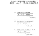
図2は、本実施形態における情報処理システムのタグの構成図を示す。図8と比べて、図2ではシステムコントローラ1内スヌープタグ5a,5bのWAY数が、対応するCPU2a,2b内のキャッシュタグ3a,3bのWAY数より1つ多い。すなわち、本実施形態では、CPU2a,2b内キャッシュタグ3a,3bのWAY数が4であるのに対し、システムコントローラ1内スヌープタグ5a,5bのWAY数は5としている。
The embodiment of the present invention will be described in detail below.
FIG. 2 shows a configuration diagram of tags of the information processing system in the present embodiment. Compared to FIG. 8, in FIG. 2, the number of WAYs in the snoop tags 5a and 5b in the
図2において、6a−Aa,6a−Abは、CPU2a,2bからのキャッシュREAD要求を示す。6a−Ba,6a−Bbは、システムコントローラからのEviction要求を示す。6a−Ca,6a−Cbは、CPU2a,2bから送信されるキャッシュデータを示す。
In FIG. 2, 6a-Aa and 6a-Ab indicate cache READ requests from the
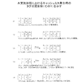
図3は、キャッシュREAD要求、Eviction要求、及びキャッシュデータのパケット形式を示す。図3(a)は、CPUからのキャッシュREAD要求6a−Aa,6a−Abのパケット形式を示す。キャッシュREAD要求は、「ID」フィールド、「OPC」フィールド、「アドレス」フィールドから構成される。「ID」フィールドは、いずれのCPUからのREAD要求であるかを識別する情報が格納されている。「OPC」フィールドには、READ命令が格納されている。「アドレス」フィールドには、読み出し要求対象のデータが格納される主メモリのアドレスが格納されている。 FIG. 3 shows a packet format of a cache READ request, an Effect request, and cache data. FIG. 3A shows the packet format of cache READ requests 6a-Aa, 6a-Ab from the CPU. The cache READ request includes an “ID” field, an “OPC” field, and an “address” field. The “ID” field stores information for identifying which CPU the READ request is from. In the “OPC” field, a READ instruction is stored. The “address” field stores the address of the main memory in which the read request target data is stored.
図3(b)は、システムコントローラからのEviction要求6a−Ba,6a−Bbのパケット形式を示す。Eviction要求は、「OPC」フィールド、「アドレス」フィールドから構成される。「OPC」フィールドには、Eviction命令が格納されている。「アドレス」フィールドには、リプレース対象となったスヌープタグのWAYに格納されたアドレスと同一のアドレスが格納されている。 FIG. 3B shows a packet format of the Effect requests 6a-Ba and 6a-Bb from the system controller. The Eviction request includes an “OPC” field and an “address” field. In the “OPC” field, an Instruction instruction is stored. The “address” field stores the same address as the address stored in the WAY of the snoop tag to be replaced.
図3(c)は、システムコントローラからCPUへ送信されるキャッシュデータ6a−Ca,6a−Cbのパケット形式を示す。キャッシュデータは、「ID」フィールド、「データ」フィールドから構成される。「データ」フィールドには、データが格納されている。
FIG. 3C shows a packet format of the
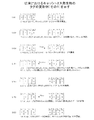
図4A及び図4Bは、本実施形態におけるキャッシュミス発生時のタグの更新例を示す。以下では、説明の便宜上、キャッシュタグ3a及びそのキャッシュタグ3aに対応するスヌープタグ5aに着目して説明する。
4A and 4B show an example of tag updating when a cache miss occurs in the present embodiment. In the following, for convenience of explanation, the
まず、CPU2a内キャッシュタグ3aは4WAYで構成され、各WAY(3a−0,3a−1,3a−2,3a−3)にはそれぞれ、アドレス(0,1,2,3)が格納されている(CPU2a内キャッシュタグ3aがFULLの状態)。
First, the
一方、システムコントローラ内スヌープタグ5aは5WAYで構成され、そのうち4つのWAY(5a−0,5a−1,5a−2,5a−3)にはそれぞれ、アドレス(0,1,2,3)が格納されている。スヌープタグ5aのWAY[5a−4]は空である。
On the other hand, the snoop
まず、CPU2aにおいて、キャッシュミスによるリード要求が発生する。例えば、アドレス5に対応するデータついてのリード要求が発生する(S1)。
そうすると、CPU2aは、例えばキャッシュタグ3aのWAY[3a−0]をリプレース対象に決定し、WAY[3a−0]に格納されているアドレス情報(アドレス0)を削除する(S2)。
First, a read request due to a cache miss occurs in the
Then, the
CPU2aは、S1で発生したアドレス情報(アドレス5)についてのリード要求をシステムコントローラ1に対して行う(S3)。
ここで、本実施形態によるシステムが、CPU2aからリプレース要求がないシステムであるとする。この場合、スヌープタグ5aがFULLの場合には、システムコントローラはスヌープタグにおける任意のWAYのアドレス情報を削除する必要がある。しかしながら、S3の状態ではスヌープタグ5aのWAY[5a−4]は空いているため、スヌープタグ5aのWAYの情報を削除する処理が発生しない。したがって、その削除処理に付随するCPU2aに対するEviction要求も発生しない。
The
Here, it is assumed that the system according to the present embodiment is a system in which there is no replacement request from the
そうすると、システムコントローラ1は、スヌープタグ5aのWAY[5a−4]を更新し、アドレス5がWAY[5a−4]に格納される。さらに、システムコントローラ1は、そのアドレスに対応するリード要求の対象データをCPU2aへ送信する(S4)。
Then, the
CPU2aは、システムコントローラ1からのデータを受信してキャッシュデータ4aに書き込むとともに、そのデータに対応するアドレス(アドレス5)によりキャッシュタグ3aのWAY[3a−0]を更新する(S5)。
The
再度、CPU2aにおいて、キャッシュミスによるリード要求が発生する。例えば、アドレス6についてのリード要求が発生する(S6)。このとき、キャッシュタグ3aがFULLであるため、CPU2aは、例えばキャッシュタグ3aのWAY[3a−1]をリプレース対象に決定し、WAY[3a−1]に格納されているアドレス情報(アドレス1)を削除する(S7)。
Again, a read request due to a cache miss occurs in the
それから、CPU2aはシステムコントローラ1へアドレス6に対応するデータのリード要求を行う(S8)。
S8の状態ではスヌープタグ5aがFULLであるため、システムコントローラ1は、例えばWAY[5a−1]をリプレース対象に決定し、そのWAY[5a−1]に格納されているアドレス情報(アドレス1)を削除する。
Then, the
In the state of S8, since the snoop
リプレース対象となったWAY[5a−1]に格納されたアドレス情報は、キャッシュタグ3aにおいてもリプレース対象となる。よって、システムコントローラ1は、リプレース対象となったアドレス(アドレス1)の削除をCPU2aへ要求する(Eviction要求)(S9)。
The address information stored in the WAY [5a-1] that is the replacement target is also the replacement target in the
CPU2aは、Eviction要求を受け取る。しかしながら、CPU2aは、Eviction要求の対象アドレスを保持していないので、Eviction処理は発生しない。すると、システムコントローラ1は、スヌープタグ5aのWAY[5a−1]を更新し、アドレス6がスヌープタグ5aのWAY[5a−1]に格納される。さらに、システムコントローラ1は、そのアドレスに対応するリード要求の対象データをCPU2aへ送信する(S10)。
The
CPU2aは、システムコントローラ1からのデータを受信してキャッシュデータ4aに書き込むとともに、そのデータに対応するアドレスによりキャッシュタグ3aのWAY[3a−0]を更新し、アドレス6がキャッシュタグ3aのWAY[3a−2]が格納される(S11)。
The
このように、キャッシュタグ3aがFULLのときにキャッシュミスが発生した場合、キャッシュタグ3aのリプレースは、キャッシュミスによるリード要求発生直後に生じるのみとなる。すなわち、キャッシュタグ3aには、タグの更新時において、生じる空きWAYは1つのみとなり、2つ以上の空きWAYが生じず、余分なリプレースは発生しない。図4A及び図4Bで説明したことを、図5を用いて説明する。
As described above, when a cache miss occurs when the
図5は、本実施形態におけるキャッシュミス発生時のタグの更新のフローを示す。まず、CPU2において、キャッシュミスによるリード要求が発生する(S21)。そうすると、CPU2はキャッシュタグ3がFULLか否かを判断する(S22)。
FIG. 5 shows a flow of updating a tag when a cache miss occurs in the present embodiment. First, the
キャッシュタグ3がFULLでない場合、すなわち、キャッシュタグ3に空きWAYがある場合(S22で「NO」へ進む)、S24へ進む。
キャッシュタグ3がFULLの場合、すなわちキャッシュタグ3に空きWAYがない場合(S22で「YES」へ進む)、キャッシュタグ3から任意のWAYを削除する(S23)。このとき、WAYの削除には、例えば、LRU(Least Recently Used)方式やその他の公知の方法で削除することができる。
When the
When the
次に、CPU2はシステムコントローラ1に対してREAD要求を行う(S24)。システムコントローラ1は、READ要求を行ったCPU2に対応するスヌープタグ5がFULLか否かを判断する(S25)。
Next, the
スヌープタグ5がFULLでない場合、すなわち、スヌープタグ5に空きWAYがある場合(S25で「NO」へ進む)、システムコントロール1はその空きWAYを更新し、READ要求されたアドレスがその空きWAYに格納される(S29)。
When the snoop
スヌープタグ5がFULLの場合、すなわち、スヌープタグ5に空きWAYがない場合(S25で「YES」へ進む)、システムコントロール1はスヌープタグ5内のWAYをランダムに選択し、選択したWAYに格納されているアドレスを削除する。さらに、システムコントローラ1は、READ要求を行ったCPU2へEviction要求を発行する(S26)。
When the snoop
そうすると、CPU2は、Eviction要求されたアドレスをキャッシュタグ3内に保持しているか否かを判断する(S27)。
Eviction要求されたアドレスがキャッシュタグ3内に保持されていない場合(S27で「NO」へ進む)、S30へ進む。
Then, the
If the address requested for the Eviction is not held in the cache tag 3 (the process proceeds to “NO” in S27), the process proceeds to S30.
Eviction要求されたアドレスがキャッシュタグ3内に保持されている場合(S27で「YES」へ進む)、CPU2は、Eviction要求されたアドレスが格納されているキャッシュタグ3のWAYのアドレスを削除する(S28)。それから、システムコントローラ1は、S26で削除したスヌープタグ5のWAYを更新する(S29)。
When the address requested for the Eviction is held in the cache tag 3 (proceeding to “YES” in S27), the
その後、システムコントローラ1はリード要求されたデータを、READ要求を行ったCPU2に送信し(S30)、さらに送信したデータに対応するアドレスでキャッシュタグ3のWAYを更新する(S31)。
Thereafter, the
なお、本実施形態では、システムコントローラ1内スヌープタグ5のWAY数をCPU2内キャッシュタグ3のWAY数より1だけ多くしたが、WAY数の関係はこれに限定されない。すなわち、スヌープタグ5のWAY数がキャッシュタグ3のWAY数より多ければよい。
In this embodiment, the number of WAYs in the snoop
また、本発明では、スヌープタグはキャッシュタグの内容と同じ内容が格納されているが、スヌープタグのWAY数が、キャッシュタグのWAY数よりも多いために、既にキャッシュでは保持されていないアドレスをも保持している。よって、スヌープタグがFULLの場合、任意に選択したWAYが、キャッシュ側で保持していないアドレスである可能性が高くなる。したがって、システムコントローラからのEviction要求が発生した場合、キャッシュ側ではそのEviction要求で指定されたアドレスを保持している可能性が低くなるため、キャッシュタグのWAYのアドレス削除処理が発生する可能性が低くなる。その結果、キャッシュタグの空きWAYが存在する可能性が低くなり、キャッシュミス率を低減させることができる。 In the present invention, the snoop tag stores the same contents as the contents of the cache tag. However, since the number of WAYs of the snoop tag is larger than the number of WAYs of the cache tag, an address that is not already held in the cache is selected. Also holds. Therefore, when the snoop tag is FULL, there is a high possibility that the arbitrarily selected WAY is an address not held on the cache side. Therefore, when an Eviction request from the system controller is generated, the cache side is less likely to hold the address specified in the Eviction request, and therefore the cache tag WAY address deletion process may occur. Lower. As a result, the possibility that there is an empty WAY of the cache tag is reduced, and the cache miss rate can be reduced.
なお、本発明は、以上に述べた実施の形態に限定されるものではなく、本発明の要旨を逸脱しない範囲内で種々の構成または態様を採ることができる。
本発明により、システムコントローラ1内のスヌープタグ5のリプレースを減少させることができる。したがって、CPU2内のキャッシュタグ3がFULLの場合に生じる過剰なリプレースの減少が可能となる。その結果、キャッシュミス率の増大を防ぐことができる。
The present invention is not limited to the above-described embodiment, and various configurations or aspects can be employed without departing from the gist of the present invention.
According to the present invention, the replacement of the snoop
(付記1) 複数ウェイからなるキャッシュタグとキャッシュデータ領域を含むキャッシュメモリを有し、外部から受け取った命令の実行及びデータの処理を行う1つ以上のプロセッサと、
前記プロセッサからの読み出し要求に基づいて該プロセッサへ応答するプロセッサ制御装置であって、該プロセッサのキャッシュタグに対応するタグ情報であるスヌープタグを有し、前記スヌープタグのウェイ数が前記プロセッサのキャッシュタグのウェイ数よりも多いプロセッサ制御装置と、
を備えることを特徴とする情報処理システム。
(Supplementary Note 1) One or more processors having a cache memory including a cache tag and a cache data area composed of a plurality of ways, and executing instructions received from outside and processing data;
A processor control device which responds to the processor based on a read request from the processor, and has a snoop tag which is tag information corresponding to the cache tag of the processor, and the number of ways of the snoop tag is the cache number of the processor More processor control units than tag ways,
An information processing system comprising:
(付記2) 前記プロセッサにおいてキャッシュミスが生じたときに、前記プロセッサから前記プロセッサ制御装置に対してデータの読み出し要求があった場合、前記プロセッサ制御装置は前記スヌープタグのウェイに空きがあれば、該空きウェイを該読み出し要求の対象となるアドレス情報で更新して、該アドレス情報に対応するデータを前記プロセッサへ送信する
ことを特徴とする付記1に記載の情報処理システム。
(Supplementary Note 2) When a cache miss occurs in the processor, if there is a data read request from the processor to the processor control device, the processor control device has an empty space in the snoop tag. The information processing system according to
(付記3) 前記空きウェイ更新時には、前記プロセッサ制御装置から前記プロセッサへ前記キャッシュタグのウェイのうち所定のアドレス情報が格納されたウェイから該アドレス情報を削除する旨の要求がなされない
ことを特徴とする付記2に記載の情報処理システム。
(Supplementary Note 3) When the empty way is updated, the processor controller does not request the processor to delete the address information from the way in which predetermined address information is stored among the ways of the cache tag. The information processing system according to
(付記4) キャッシュミス時に前記プロセッサから読み出し要求があった場合、前記スヌープタグのウェイに空きがなければ、前記プロセッサ制御装置は前記スヌープタグのウェイに格納されたアドレス情報のいずれかを削除し、該アドレス情報を削除する旨を前記プロセッサへ通知する
ことを特徴とする付記1に記載の情報処理システム。
(Supplementary Note 4) When there is a read request from the processor at the time of a cache miss, if there is no free space in the snoop tag way, the processor control device deletes any of the address information stored in the snoop tag way The information processing system according to
(付記5) 前記情報処理システムには、キャッシュミス時に前記キャッシュタグのいずれかのウェイに格納されたアドレス情報を追い出す旨の情報を前記プロセッサから前記プロセッサ制御装置へ通知しない方式が用いられている
ことを特徴とする付記1に記載の情報処理システム。
(Additional remark 5) The said information processing system uses the system which does not notify the said processor control apparatus of the information to drive out the address information stored in one of the ways of the said cache tag at the time of a cache miss The information processing system according to
(付記6) キャッシュタグとキャッシュデータ領域からなる複数ウェイのキャッシュメモリを有し、命令を実行及びデータを処理する1つ以上のプロセッサと、前記プロセッサからの要求に基づいて該プロセッサへ情報を送信するプロセッサ制御装置であって、該各プロセッサのキャッシュタグに対応するタグ情報であるスヌープタグのウェイ数が前記プロセッサのキャッシュタグのウェイ数よりも多い該スヌープタグを有する該プロセッサ制御装置と、を備える情報処理システムのキャッシュタグ及びスヌープタグの更新方法であって、
キャッシュミス時に前記プロセッサから読み出し要求があった場合、前記スヌープタグのウェイに空きがあれば、前記プロセッサ制御装置は該空きウェイを該読み出し要求の対象となるアドレス情報で更新して、該アドレス情報に対応するデータを前記プロセッサへ送信する
ことを特徴とするキャッシュタグ及びスヌープタグの更新方法。
(Supplementary note 6) One or more processors having a multi-way cache memory including a cache tag and a cache data area, executing instructions and processing data, and transmitting information to the processors based on requests from the processors A processor control device having a snoop tag in which the number of ways of the snoop tag, which is tag information corresponding to the cache tag of each processor, is greater than the number of ways of the cache tag of the processor. A method for updating a cache tag and a snoop tag of an information processing system comprising:
When there is a read request from the processor at the time of a cache miss, if there is a vacancy in the way of the snoop tag, the processor control device updates the vacant way with the address information targeted for the read request, and the address information A method for updating a cache tag and a snoop tag, comprising: transmitting data corresponding to the processor to the processor.
(付記7) 前記空きウェイ更新時には、前記プロセッサ制御装置から前記プロセッサへ前記キャッシュタグのウェイのうち所定のアドレス情報が格納されたウェイから該アドレス情報を削除する旨の要求がなされない
ことを特徴とする付記6に記載のキャッシュタグ及びスヌープタグの更新方法。
(Supplementary Note 7) When the empty way is updated, the processor control device does not request the processor to delete the address information from the way in which predetermined address information is stored among the ways of the cache tag. The method for updating a cache tag and a snoop tag according to
(付記8) キャッシュミス時に前記プロセッサから情報の読み出し要求があった場合、前記スヌープタグのウェイに空きがなければ、前記プロセッサ制御装置は前記スヌープタグのウェイに格納されたアドレス情報のいずれかを削除し、該アドレスを削除する旨を前記プロセッサへ通知する
ことを特徴とする付記6に記載のキャッシュタグ及びスヌープタグの更新方法。
(Supplementary Note 8) When there is a request to read information from the processor at the time of a cache miss, if there is no space in the way of the snoop tag, the processor control device can store one of the address information stored in the way of the snoop tag. The cache tag and snoop tag update method according to
(付記9) 前記情報処理システムには、キャッシュミス時に前記キャッシュタグのいずれかを追い出す旨の情報を前記プロセッサ制御装置へ通知しない方式が用いられている
ことを特徴とする付記6に記載のキャッシュタグ及びスヌープタグの更新方法。
(Supplementary note 9) The cache according to
(付記10) 複数ウェイからなるキャッシュタグとキャッシュデータ領域を含むキャッシュメモリを有し、外部から受け取った命令を実行及びデータを処理する1つ以上のプロセッサと、
前記プロセッサからの読み出し要求に基づいて該プロセッサへ応答するプロセッサ制御装置であって、該各プロセッサのキャッシュタグに対応するタグ情報であるスヌープタグのウェイ数が前記プロセッサのキャッシュタグのウェイ数よりも多い該スヌープタグを有する該プロセッサ制御装置と、
を備えることを特徴とする情報処理基板。
(Supplementary Note 10) One or more processors that have a cache memory including a cache tag and a cache data area including a plurality of ways, execute an instruction received from the outside, and process data.
A processor control apparatus that responds to the processor based on a read request from the processor, wherein the number of ways of the snoop tag that is tag information corresponding to the cache tag of each processor is greater than the number of ways of the cache tag of the processor The processor controller having a number of the snoop tags;
An information processing board comprising:
(付記11) キャッシュミス時に前記プロセッサから読み出し要求があった場合、前記プロセッサ制御装置は前記スヌープタグのウェイに空きがあれば、該空きウェイを該読み出し要求の対象となるアドレス情報で更新して、該アドレス情報に対応するデータを前記プロセッサへ送信する
ことを特徴とする付記10に記載の情報処理基板。
(Supplementary Note 11) If there is a read request from the processor at the time of a cache miss, the processor control device updates the free way with the address information that is the target of the read request if there is a free space in the snoop tag. The data processing board according to
(付記12) 前記空きウェイ更新時には、前記プロセッサ制御装置から前記プロセッサへ前記キャッシュタグのウェイのうち所定のアドレス情報が格納されたウェイから該アドレス情報を削除する旨の要求がなされない
ことを特徴とする付記11に記載の情報処理基板。
(Additional remark 12) At the time of the said empty way update, the request | requirement of deleting this address information from the way in which the predetermined address information was stored among the ways of the said cache tag from the said processor control apparatus to the said processor is made. The information processing board according to
(付記13) キャッシュミス時に前記プロセッサから読み出し要求があった場合、前記スヌープタグのウェイに空きがなければ、前記プロセッサ制御装置は前記スヌープタグのウェイに格納されたアドレス情報のいずれかを削除し、該アドレス情報を削除する旨を前記プロセッサへ通知する
ことを特徴とする付記10に記載の情報処理基板。
(Supplementary note 13) When there is a read request from the processor at the time of a cache miss, if there is no free space in the snoop tag way, the processor control device deletes any of the address information stored in the snoop tag way The information processing board according to
(付記14) 前記情報処理システムには、キャッシュミス時に前記キャッシュタグのいずれかのウェイに格納されたアドレス情報を追い出す旨の情報を前記プロセッサから前記プロセッサ制御装置へ通知しない方式が用いられている
ことを特徴とする付記10に記載の情報処理基板。
(Additional remark 14) The said information processing system uses the system which does not notify the said processor control apparatus of the information which drives out the address information stored in either way of the said cache tag at the time of a cache miss The information processing board according to
100 情報処理システム
101 プロセッサ制御装置
102 スヌープタグ
103 ウェイ
104 プロセッサ
105 キャッシュタグ
106 ウェイ
1 システムコントローラ
2(2a,2b,2c,2d) CPU
3(3a,3b,3c,3d) キャッシュタグ
4(4a,4b,4c,4d) キャッシュデータ
5(5a,5b,5c,5d) スヌープタグ
6(6a,6b,6c,6d) CPUバス
DESCRIPTION OF
3 (3a, 3b, 3c, 3d) Cache tag 4 (4a, 4b, 4c, 4d) Cache data 5 (5a, 5b, 5c, 5d) Snoop tag 6 (6a, 6b, 6c, 6d) CPU bus
Claims (10)
前記プロセッサからの読み出し要求に基づいて該プロセッサへ応答するプロセッサ制御装置であって、該プロセッサのキャッシュタグに対応するタグ情報であるスヌープタグを有し、前記スヌープタグのウェイ数が前記プロセッサのキャッシュタグのウェイ数よりも多いプロセッサ制御装置と、
を備えることを特徴とする情報処理システム。 One or more processors having a cache memory including a cache tag and a cache data area composed of a plurality of ways, and executing an instruction received from outside and processing data;
A processor control device which responds to the processor based on a read request from the processor, and has a snoop tag which is tag information corresponding to the cache tag of the processor, and the number of ways of the snoop tag is the cache number of the processor More processor control units than tag ways,
An information processing system comprising:
ことを特徴とする請求項1に記載の情報処理システム。 If there is a data read request from the processor to the processor control device when a cache miss occurs in the processor, the processor control device sets the free way if there is a free space in the snoop tag. The information processing system according to claim 1, wherein the information is updated with the address information that is the target of the read request, and data corresponding to the address information is transmitted to the processor.
ことを特徴とする請求項2に記載の情報処理システム。 The request for deleting the address information from the way in which predetermined address information is stored among the ways of the cache tag is not made from the processor control unit to the processor when the empty way is updated. 2. The information processing system according to 2.
ことを特徴とする請求項1に記載の情報処理システム。 When there is a read request from the processor at the time of a cache miss, if there is no space in the way of the snoop tag, the processor control device deletes any of the address information stored in the way of the snoop tag, and the address information The information processing system according to claim 1, wherein the processor is notified of the fact that it is deleted.
ことを特徴とする請求項1に記載の情報処理システム。 The information processing system uses a method in which the processor does not notify the processor control device of information indicating that the address information stored in any of the ways of the cache tag is expelled when a cache miss occurs. The information processing system according to claim 1.
キャッシュミス時に前記プロセッサから読み出し要求があった場合、前記スヌープタグのウェイに空きがあれば、前記プロセッサ制御装置は該空きウェイを該読み出し要求の対象となるアドレス情報で更新して、該アドレス情報に対応するデータを前記プロセッサへ送信する
ことを特徴とするキャッシュタグ及びスヌープタグの更新方法。 One or more processors for executing instructions and processing data, and a processor control device for transmitting information to the processor based on a request from the processor, having a cache memory having a plurality of ways including a cache tag and a cache data area An information processing system comprising: the processor control device having the snoop tag in which the number of ways of the snoop tag, which is tag information corresponding to the cache tag of each processor, is greater than the number of ways of the cache tag of the processor. The cache tag and snoop tag update method of
When there is a read request from the processor at the time of a cache miss, if there is a vacancy in the way of the snoop tag, the processor control device updates the vacant way with the address information targeted for the read request, and the address information A method for updating a cache tag and a snoop tag, comprising: transmitting data corresponding to the processor to the processor.
ことを特徴とする請求項6に記載のキャッシュタグ及びスヌープタグの更新方法。 The request for deleting the address information from the way in which predetermined address information is stored among the ways of the cache tag is not made from the processor control unit to the processor when the empty way is updated. 6. A method for updating a cache tag and a snoop tag according to 6.
ことを特徴とする請求項6に記載のキャッシュタグ及びスヌープタグの更新方法。 When there is a request for reading information from the processor at the time of a cache miss, if there is no free space in the snoop tag way, the processor control device deletes any of the address information stored in the snoop tag way, The cache tag and snoop tag update method according to claim 6, wherein the processor is notified that an address is to be deleted.
ことを特徴とする請求項6に記載のキャッシュタグ及びスヌープタグの更新方法。 The cache tag and snoop according to claim 6, wherein the information processing system uses a method of not notifying the processor control device of information that drives out one of the cache tags when a cache miss occurs. How to update tags.
前記プロセッサからの読み出し要求に基づいて該プロセッサへ応答するプロセッサ制御装置であって、該各プロセッサのキャッシュタグに対応するタグ情報であるスヌープタグのウェイ数が前記プロセッサのキャッシュタグのウェイ数よりも多い該スヌープタグを有する該プロセッサ制御装置と、
を備えることを特徴とする情報処理基板。 One or more processors having a cache memory including a cache tag and a cache data area composed of a plurality of ways, executing instructions received from the outside, and processing data;
A processor control apparatus that responds to the processor based on a read request from the processor, wherein the number of ways of the snoop tag that is tag information corresponding to the cache tag of each processor is greater than the number of ways of the cache tag of the processor The processor controller having a number of the snoop tags;
An information processing board comprising:
Priority Applications (5)
| Application Number | Priority Date | Filing Date | Title |
|---|---|---|---|
| JP2006222439A JP2008046902A (en) | 2006-08-17 | 2006-08-17 | Information processing system, information processing board, cache tag, and method for updating snoop tag |
| EP07106976A EP1895419B1 (en) | 2006-08-17 | 2007-04-26 | Information processing system, information processing board, and method of updating cache tag and snoop tag |
| US11/740,984 US7805576B2 (en) | 2006-08-17 | 2007-04-27 | Information processing system, information processing board, and method of updating cache tag and snoop tag |
| KR1020070045444A KR100900012B1 (en) | 2006-08-17 | 2007-05-10 | Information processing system, information processing board, and method of updating cache tag and snoop tag |
| CN200710103962XA CN101127011B (en) | 2006-08-17 | 2007-05-17 | Information processing board, information processing system, and method of updating tag |
Applications Claiming Priority (1)
| Application Number | Priority Date | Filing Date | Title |
|---|---|---|---|
| JP2006222439A JP2008046902A (en) | 2006-08-17 | 2006-08-17 | Information processing system, information processing board, cache tag, and method for updating snoop tag |
Publications (1)
| Publication Number | Publication Date |
|---|---|
| JP2008046902A true JP2008046902A (en) | 2008-02-28 |
Family
ID=38691934
Family Applications (1)
| Application Number | Title | Priority Date | Filing Date |
|---|---|---|---|
| JP2006222439A Pending JP2008046902A (en) | 2006-08-17 | 2006-08-17 | Information processing system, information processing board, cache tag, and method for updating snoop tag |
Country Status (5)
| Country | Link |
|---|---|
| US (1) | US7805576B2 (en) |
| EP (1) | EP1895419B1 (en) |
| JP (1) | JP2008046902A (en) |
| KR (1) | KR100900012B1 (en) |
| CN (1) | CN101127011B (en) |
Families Citing this family (2)
| Publication number | Priority date | Publication date | Assignee | Title |
|---|---|---|---|---|
| JP5011885B2 (en) * | 2006-08-18 | 2012-08-29 | 富士通株式会社 | Snoop tag control device |
| JP5790532B2 (en) * | 2012-02-13 | 2015-10-07 | セイコーエプソン株式会社 | Electronic device and memory control method |
Citations (6)
| Publication number | Priority date | Publication date | Assignee | Title |
|---|---|---|---|---|
| JPS5373927A (en) * | 1976-11-10 | 1978-06-30 | Fujitsu Ltd | Replacing system of intermediate buffer memory |
| JPH02188847A (en) * | 1989-01-18 | 1990-07-24 | Agency Of Ind Science & Technol | Data exchange system for hierarchical cache memory |
| JPH05216765A (en) * | 1992-02-06 | 1993-08-27 | Hitachi Ltd | Hierarchical buffer storage device |
| JPH11306082A (en) * | 1998-04-23 | 1999-11-05 | Fujitsu Ltd | Main storage control device |
| JP2002007371A (en) * | 2000-06-23 | 2002-01-11 | Hitachi Ltd | L1 cache false share relaxing and control system |
| JP2002055880A (en) * | 2000-08-08 | 2002-02-20 | Hitachi Ltd | Cache constituting method and processor system |
Family Cites Families (9)
| Publication number | Priority date | Publication date | Assignee | Title |
|---|---|---|---|---|
| JP2862424B2 (en) | 1992-01-30 | 1999-03-03 | 株式会社日立製作所 | Information processing device |
| JPH05265970A (en) | 1992-03-19 | 1993-10-15 | Toshiba Corp | Multi-processor system |
| US5590310A (en) | 1993-01-14 | 1996-12-31 | Integrated Device Technology, Inc. | Method and structure for data integrity in a multiple level cache system |
| JPH0713864A (en) * | 1993-06-25 | 1995-01-17 | Mitsubishi Electric Corp | Data processor |
| TW243509B (en) | 1994-01-31 | 1995-03-21 | Ibm | Data processor with memory cache and method of operation |
| US5860109A (en) | 1996-07-01 | 1999-01-12 | Sun Microsystems, Inc. | Methods and apparatus for a coherence transformer for connecting computer system coherence domains |
| JPH1173370A (en) * | 1997-08-29 | 1999-03-16 | Fujitsu Ltd | Information processor |
| JP3989312B2 (en) | 2002-07-05 | 2007-10-10 | 富士通株式会社 | Cache memory device and memory allocation method |
| US7143246B2 (en) * | 2004-01-16 | 2006-11-28 | International Business Machines Corporation | Method for supporting improved burst transfers on a coherent bus |
-
2006
- 2006-08-17 JP JP2006222439A patent/JP2008046902A/en active Pending
-
2007
- 2007-04-26 EP EP07106976A patent/EP1895419B1/en not_active Expired - Fee Related
- 2007-04-27 US US11/740,984 patent/US7805576B2/en not_active Expired - Fee Related
- 2007-05-10 KR KR1020070045444A patent/KR100900012B1/en active IP Right Grant
- 2007-05-17 CN CN200710103962XA patent/CN101127011B/en not_active Expired - Fee Related
Patent Citations (6)
| Publication number | Priority date | Publication date | Assignee | Title |
|---|---|---|---|---|
| JPS5373927A (en) * | 1976-11-10 | 1978-06-30 | Fujitsu Ltd | Replacing system of intermediate buffer memory |
| JPH02188847A (en) * | 1989-01-18 | 1990-07-24 | Agency Of Ind Science & Technol | Data exchange system for hierarchical cache memory |
| JPH05216765A (en) * | 1992-02-06 | 1993-08-27 | Hitachi Ltd | Hierarchical buffer storage device |
| JPH11306082A (en) * | 1998-04-23 | 1999-11-05 | Fujitsu Ltd | Main storage control device |
| JP2002007371A (en) * | 2000-06-23 | 2002-01-11 | Hitachi Ltd | L1 cache false share relaxing and control system |
| JP2002055880A (en) * | 2000-08-08 | 2002-02-20 | Hitachi Ltd | Cache constituting method and processor system |
Also Published As
| Publication number | Publication date |
|---|---|
| EP1895419A3 (en) | 2008-03-26 |
| US7805576B2 (en) | 2010-09-28 |
| KR100900012B1 (en) | 2009-05-29 |
| EP1895419B1 (en) | 2013-01-23 |
| US20080046662A1 (en) | 2008-02-21 |
| KR20080016429A (en) | 2008-02-21 |
| EP1895419A2 (en) | 2008-03-05 |
| CN101127011A (en) | 2008-02-20 |
| CN101127011B (en) | 2010-06-02 |
Similar Documents
| Publication | Publication Date | Title |
|---|---|---|
| US8762651B2 (en) | Maintaining cache coherence in a multi-node, symmetric multiprocessing computer | |
| US20110173393A1 (en) | Cache memory, memory system, and control method therefor | |
| JP2007524904A (en) | Method and apparatus for dynamic prefetch buffer configuration and replacement | |
| JP2009098934A (en) | Processor and cache memory | |
| JP2007011580A (en) | Information processing device | |
| KR101472967B1 (en) | Cache memory and method capable of write-back operation, and system having the same | |
| JP5163220B2 (en) | Cache control device, information processing device | |
| JP5499987B2 (en) | Shared cache memory device | |
| US20150370707A1 (en) | Disunited shared-information and private-information caches | |
| JP4295814B2 (en) | Multiprocessor system and method of operating multiprocessor system | |
| JP5040121B2 (en) | Information processing apparatus, cache control method, and program | |
| JP2006099802A (en) | Storage controller, and control method for cache memory | |
| JP2008046902A (en) | Information processing system, information processing board, cache tag, and method for updating snoop tag | |
| US20130339624A1 (en) | Processor, information processing device, and control method for processor | |
| US20180335829A1 (en) | Processing device and control method of processing device | |
| US9983994B2 (en) | Arithmetic processing device and method for controlling arithmetic processing device | |
| JP2008026970A (en) | Storage device | |
| JP5168800B2 (en) | Multiprocessor system | |
| JP4295815B2 (en) | Multiprocessor system and method of operating multiprocessor system | |
| JP2008176612A (en) | Multiprocessor system | |
| JP2007257192A (en) | Data processor | |
| JP2005149290A (en) | Information processing device and cache memory control method | |
| JP2004171469A (en) | Cache memory system and cache memory control method | |
| WO2007110914A1 (en) | Multiprocessor system and multiprocessor system operating method | |
| JP2014170262A (en) | Bus module and data processor |
Legal Events
| Date | Code | Title | Description |
|---|---|---|---|
| A621 | Written request for application examination |
Free format text: JAPANESE INTERMEDIATE CODE: A621 Effective date: 20090409 |
|
| A977 | Report on retrieval |
Free format text: JAPANESE INTERMEDIATE CODE: A971007 Effective date: 20111227 |
|
| A131 | Notification of reasons for refusal |
Free format text: JAPANESE INTERMEDIATE CODE: A131 Effective date: 20120117 |
|
| A521 | Written amendment |
Free format text: JAPANESE INTERMEDIATE CODE: A523 Effective date: 20120319 |
|
| A02 | Decision of refusal |
Free format text: JAPANESE INTERMEDIATE CODE: A02 Effective date: 20120508 |
|
| A521 | Written amendment |
Free format text: JAPANESE INTERMEDIATE CODE: A523 Effective date: 20120808 |
|
| A911 | Transfer of reconsideration by examiner before appeal (zenchi) |
Free format text: JAPANESE INTERMEDIATE CODE: A911 Effective date: 20120815 |
|
| A912 | Removal of reconsideration by examiner before appeal (zenchi) |
Free format text: JAPANESE INTERMEDIATE CODE: A912 Effective date: 20120907 |