JP2008028362A - Magnetoresistive element and magnetic memory - Google Patents
Magnetoresistive element and magnetic memory Download PDFInfo
- Publication number
- JP2008028362A JP2008028362A JP2007044176A JP2007044176A JP2008028362A JP 2008028362 A JP2008028362 A JP 2008028362A JP 2007044176 A JP2007044176 A JP 2007044176A JP 2007044176 A JP2007044176 A JP 2007044176A JP 2008028362 A JP2008028362 A JP 2008028362A
- Authority
- JP
- Japan
- Prior art keywords
- layer
- magnetization
- pinned layer
- magnetoresistive element
- pinned
- Prior art date
- Legal status (The legal status is an assumption and is not a legal conclusion. Google has not performed a legal analysis and makes no representation as to the accuracy of the status listed.)
- Abandoned
Links
Images
Abstract
Description
本発明は、磁気抵抗素子及び磁気メモリに係り、例えば双方向に電流を供給することで情報を記録することが可能な磁気抵抗素子及びそれを用いた磁気メモリに関する。 The present invention relates to a magnetoresistive element and a magnetic memory, and more particularly, to a magnetoresistive element capable of recording information by supplying current bidirectionally and a magnetic memory using the same.
近年、新しい原理に基づいて情報を記録する固体メモリが多数提案されているが、中でも、固体磁気メモリとして、トンネル磁気抵抗(TMR:Tunneling Magnetoresistive)効果を利用する磁気ランダムアクセスメモリ(MRAM:Magnetoresistive Random Access Memory)が脚光を浴びている。MRAMは、データをMTJ(Magnetic Tunnel Junction)素子の磁化状態により記憶する点に特徴を有する。 In recent years, many solid-state memories that record information based on a new principle have been proposed. Among them, as a solid-state magnetic memory, a magnetic random access memory (MRAM: Magnetoresistive Random) that uses a tunneling magnetoresistive (TMR) effect is proposed. Access Memory) is in the spotlight. The MRAM is characterized in that data is stored according to the magnetization state of an MTJ (Magnetic Tunnel Junction) element.
従来型の配線電流による磁場で書き込みを行うMRAMにおいては、MTJ素子サイズを縮小すると保持力Hcが大きくなるために、書き込みに必要な電流が大きくなる傾向がある。実際には、256Mbits以上の大容量を有するMRAMを作製するには、チップサイズの縮小が必要であり、それを実現するためにはチップ内におけるセルアレイ占有率を上げ、MTJ素子サイズの縮小を抑えつつ、書き込み電流のμAレベルへの低減が必要である。MTJ素子サイズの縮小と書き込み電流の低減は、相反的な関係にあり、従来型MRAMでは、256Mbitsを超えるような大容量化に向けたセルサイズの微細化と低電流化の両立は困難である。 In an MRAM in which writing is performed with a magnetic field using a conventional wiring current, the holding force Hc increases when the MTJ element size is reduced, and therefore, the current required for writing tends to increase. Actually, in order to manufacture an MRAM having a large capacity of 256 Mbits or more, it is necessary to reduce the chip size. In order to realize this, the cell array occupancy in the chip is increased and the reduction in the MTJ element size is suppressed. However, it is necessary to reduce the write current to the μA level. The reduction in the MTJ element size and the reduction in the write current are in a reciprocal relationship, and it is difficult for the conventional MRAM to achieve both a reduction in the cell size and a reduction in the current to increase the capacity exceeding 256 Mbits. .
このような課題を克服する書き込み方式としてスピン角運動量移動(SMT:Spin Momentum Transfer)書き込み方式を用いたMRAMが提案されている(例えば、特許文献1、非特許文献1〜2)。スピン角運動量移動(以下、スピン注入と称する)磁化反転では、磁化反転に必要な反転電流Icは、電流密度Jcで規定される。従って、素子面積が小さくなれば、スピン注入により磁化反転するための反転電流Icも小さくなる。
As a writing method for overcoming such a problem, an MRAM using a spin momentum transfer (SMT) writing method has been proposed (for example,
先に述べた従来型の磁場書き込み方式に比べると、電流密度を一定にして書き込む場合、MTJ素子サイズが小さくなれば書き込み電流も小さくなるために、スケーラビリティ性に優れることが期待される。しかしながら、現状のスピン注入MRAMにおいては、その磁化反転に必要な電流密度Jcは10mA/cm2以上と非常に大きく、100nm2サイズのMTJ素子を用いた場合でも、書き込み電流としては1mA程度必要となる。 Compared to the above-described conventional magnetic field writing method, when writing with a constant current density, the write current is reduced as the MTJ element size is reduced, so that it is expected to have excellent scalability. However, in the current spin injection MRAM, the current density Jc necessary for the magnetization reversal is as large as 10 mA / cm 2 or more, and even when a 100 nm 2 size MTJ element is used, a write current of about 1 mA is required. Become.
これは、スピン注入磁化反転方式の場合、双方向の通電が必要となり、通電方向によりスピン注入効率が異なることに起因している。すなわち、スピン注入磁化反転カーブは非対称となる。これは、磁化自由層(以下、フリー層と称する)と磁化参照層(以下、ピン層と称する)との磁化配列が平行から反平行になるようにフリー層の磁化の方向を反転させる場合の電流は、反平行から平行に反転させる場合に比べて2倍程度必要となる。 This is because the spin injection magnetization reversal method requires bidirectional energization, and the spin injection efficiency differs depending on the energization direction. That is, the spin injection magnetization reversal curve is asymmetric. This is because the magnetization direction of the free layer is reversed so that the magnetization arrangement of the magnetization free layer (hereinafter referred to as the free layer) and the magnetization reference layer (hereinafter referred to as the pinned layer) changes from parallel to antiparallel. The current is required to be about twice that in the case where the current is reversed from antiparallel to parallel.
この非対称性に伴う問題として、トンネル磁気抵抗(TMR)効果膜を用いる場合、フリー層とピン層との磁化配列を反平行から平行に反転させるために通電して書き込む場合は、電流閾値が小さく問題がない。しかし、フリー層とピン層との磁化配列を平行から反平行に反転させるために通電して書き込む場合には、大きな書き込み電流が原因となり、一定の電流密度Ia-apで書き込むとすると、TMR効果に見合った分だけ反平行配列時の素子抵抗Rapが上昇することになり、結果的に、書き込み電圧Vp-apは上昇する。 A problem associated with this asymmetry is that when a tunnel magnetoresistive (TMR) effect film is used, the current threshold is small when writing is performed by energizing to reverse the magnetization arrangement of the free layer and the pinned layer from antiparallel to parallel. there is no problem. However, in the case of writing with energization to reverse the magnetization arrangement of the free layer and the pinned layer from parallel to antiparallel, a large write current is the cause. If writing is performed at a constant current density Ia-ap, the TMR effect As a result, the element resistance Rap in the antiparallel arrangement increases by the amount corresponding to the above, and as a result, the write voltage Vp-ap increases.
従って、トンネルバリア層の耐圧が十分高くない場合、反平行磁化配列になる前に、トンネルバリア層の破壊電圧Vbdに到達してしまい、トンネルバリア層が絶縁破壊するという課題を有している。また、たとえ絶縁破壊しなくとも、高電圧下での動作信頼性が確保されないという問題がある。
本発明は、上記のような事情に鑑みてなされたもので、磁化反転の際の反転電流をより低減することが可能な磁気抵抗素子及びそれを用いた磁気メモリを提供することを目的とする。 The present invention has been made in view of the above circumstances, and an object thereof is to provide a magnetoresistive element capable of further reducing a reversal current at the time of magnetization reversal and a magnetic memory using the same. .
本発明の第1の視点に係る磁気抵抗素子は、磁化の方向が固定された第1の磁化参照層と、スピン偏極した電子の作用により磁化の方向が変化する磁化自由層と、磁化の方向が固定された第2の磁化参照層と、前記第1の磁化参照層と前記磁化自由層との間に設けられた第1の中間層と、前記磁化自由層と前記第2の磁化参照層との間に設けられた第2の中間層と、を具備し、前記磁化自由層及び前記第1の磁化参照層の容易磁化方向は、膜面に対して垂直或いは平行であり、前記第1の磁化参照層と前記第2の磁化参照層との容易磁化方向は、互いに直交することを特徴とする。 A magnetoresistive element according to a first aspect of the present invention includes a first magnetization reference layer in which the magnetization direction is fixed, a magnetization free layer in which the magnetization direction changes due to the action of spin-polarized electrons, A second magnetization reference layer having a fixed direction, a first intermediate layer provided between the first magnetization reference layer and the magnetization free layer, the magnetization free layer, and the second magnetization reference A second intermediate layer provided between the magnetization free layer and the first magnetization reference layer. The easy magnetization direction of the magnetization free layer and the first magnetization reference layer is perpendicular or parallel to the film surface, and The easy magnetization directions of one magnetization reference layer and the second magnetization reference layer are orthogonal to each other.
本発明の第2の視点に係る磁気メモリは、上記第1の視点に係る磁気抵抗素子と、この磁気抵抗素子に対して通電を行う第1及び第2の電極とを含むメモリセルを具備することを特徴とする。 A magnetic memory according to a second aspect of the present invention includes a memory cell including the magnetoresistive element according to the first aspect, and first and second electrodes for energizing the magnetoresistive element. It is characterized by that.
本発明によれば、磁化反転の際の反転電流をより低減することが可能な磁気抵抗素子及びそれを用いた磁気メモリを提供することができる。 ADVANTAGE OF THE INVENTION According to this invention, the magnetoresistive element which can reduce the reversal current at the time of magnetization reversal, and a magnetic memory using the same can be provided.
以下、本発明の実施の形態について図面を参照して説明する。なお、以下の説明において、同一の機能及び構成を有する要素については、同一符号を付し、重複説明は必要な場合にのみ行う。 Hereinafter, embodiments of the present invention will be described with reference to the drawings. In the following description, elements having the same function and configuration are denoted by the same reference numerals, and redundant description will be given only when necessary.
(第1の実施形態)
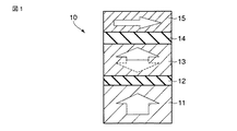
図1は、本発明の第1の実施形態に係るMTJ素子10の構成を示す断面図である。図1は、本実施形態のMTJ素子10の基本構成を示している。なお、図中の矢印は、磁化の方向を示している。
(First embodiment)
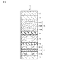
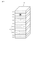
FIG. 1 is a cross-sectional view showing a configuration of an
MTJ素子10は、第1の磁化参照層(ピン層)11、第1の中間層12、磁化自由層(フリー層)13、第2の中間層14、第2の磁化参照層15が順に積層された積層構造を有している。なお、この基本構成は、積層順序が逆転していても構わない。
In the
ピン層11とピン層15とは、磁化(或いはスピン)の方向が固着されている。フリー層13は、磁化の方向が変化(反転)する。また、ピン層11及びフリー層13の容易磁化方向は膜面(或いは積層面)に対して垂直であり(以下、垂直磁化と称する)、ピン層15の容易磁化方向は膜面に対して平行である(以下、面内磁化と称する)。すなわち、ピン層11とピン層15とは、容易磁化方向が互いに直交している。
The
なお、容易磁化方向とは、あるマクロなサイズの強磁性体を想定して、外部磁界のない状態で自発磁化がその方向を向くと最も内部エネルギーが低くなる方向である。困難磁化方向とは、あるマクロなサイズの強磁性体を想定して、外部磁界のない状態で自発磁化がその方向を向くと最も内部エネルギーが大きくなる方向である。 Note that the easy magnetization direction is a direction in which the internal energy is lowest when the spontaneous magnetization is directed in the absence of an external magnetic field, assuming a macro-sized ferromagnetic material. The difficult magnetization direction is a direction in which the internal energy is maximized when the spontaneous magnetization is directed in the absence of an external magnetic field, assuming a macro-sized ferromagnetic material.
本実施形態では、フリー層13として垂直磁化膜を用いている。フリー層13に垂直磁化膜を用いることにより、MTJ素子サイズのアスペクト比Ar(素子の短辺長と長辺長との比、すなわち、Ar=長辺長/短辺長)を1に設計することが可能となる。これは、面内磁化膜の場合は、熱的に安定するのに必要な異方性磁界(Hk)は形状磁気異方性エネルギーにより賄われるために、MTJ素子のアスペクト比が1より大きくなる。これに対して、垂直磁化膜の場合は、熱的に安定するのに必要な異方性磁界(Hk)は結晶磁気異方性エネルギーにより賄われるために、この異方性磁界(Hk)はMTJ素子のアスペクト比に依存しないからである。
In the present embodiment, a perpendicular magnetization film is used as the
この結果、MTJ素子サイズを微細化することが可能となる。この場合、スピン注入による磁化反転に必要な電流密度Jcが同じTMR膜を用いたならば、同じMTJ素子幅を有する面内磁化膜と垂直磁化膜とでは、スピン注入反転電流Icは、垂直磁化膜の方がアスペクト比Arが小さくなるので低減される。 As a result, the MTJ element size can be reduced. In this case, if a TMR film having the same current density Jc required for magnetization reversal by spin injection is used, the spin injection reversal current Ic is perpendicular magnetization between the in-plane magnetization film and the perpendicular magnetization film having the same MTJ element width. The film is reduced because the aspect ratio Ar becomes smaller.
このように構成されたMTJ素子10において、データの書き込みは、以下のように行われる。なお、本実施形態において、電流は、電子の流れをいうものとする。先ず、MTJ素子10は、膜面(或いは積層面)に垂直な方向において、双方向に電流通電される。
In the
これにより、フリー層13に、マジョリティーとマイノリティーに偏極した電子スピンが供給される。そして、マジョリティーな電子スピンのスピン角運動量がフリー層13に移動することにより、スピントルクがフリー層13に印加され、フリー層13の磁化回転を誘起する。スピントルクは、ピン層とフリー層との磁化方向の単位ベクトルの外積で表されるので、2つの直交するピン層の両方からフリー層にスピントルクを印加できる。これにより、スピン注入による磁化反転電流を低減できる。
As a result, electron spins polarized in majority and minority are supplied to the
具体的には、ピン層11側から電子(すなわち、ピン層11からフリー層13へ向かう電子)を供給した場合、ピン層11の容易磁化方向と同じ方向にスピン偏極された電子と、ピン層15により反射されることでピン層15の容易磁化方向と反対方向にスピン偏極された電子とがフリー層13に注入される。この場合、フリー層13の磁化の方向は、ピン層11の容易磁化方向と同じ方向に揃えられる。これにより、ピン層11とフリー層13との磁化の方向が平行配列となる。この平行配列のときはMTJ素子10の抵抗値は最も小さくなり、この場合をデータ“0”と規定する。
Specifically, when electrons are supplied from the pinned
一方、ピン層15側から電子(すなわち、ピン層15からフリー層13へ向かう電子)を供給した場合、ピン層15の容易磁化方向と同じ方向にスピン偏極された電子と、ピン層11により反射されることでピン層11の容易磁化方向と反対方向にスピン偏極された電子とがフリー層13に注入される。この場合、フリー層13の磁化の方向は、ピン層11の容易磁化方向と反対方向に揃えられる。これにより、ピン層11とフリー層13との磁化の方向が反平行配列となる。この反平行配列のときはMTJ素子10の抵抗値は最も大きくなり、この場合をデータ“1”と規定する。
On the other hand, when electrons are supplied from the pinned
次に、データの読み出しは、以下のように行われる。MTJ素子10に読み出し電流を流し、MTJ素子10の抵抗値の変化を検出する。この読み出し電流は、書き込み電流よりも小さい値に設定される。
Next, data reading is performed as follows. A read current is passed through the
ここで、フリー層13の容易磁化方向は膜面に対して垂直であるので、磁化配列が平行となるピン層11との間では中間層12を介して磁気抵抗効果が発現するが、磁化配列が垂直となるピン層15との間では中間層14を介した磁気抵抗効果は発現しない。これは、大きなメリットであり、デュアルピン層構造(すなわち、フリー層の両側にそれぞれ中間層を介して2つのピン層が配置される構造)を有する磁気抵抗効果素子で問題であった2つ目のピン層による読み出し出力の劣化を回避することが可能となる。
Here, since the easy magnetization direction of the
すなわち、本実施形態のMTJ素子10においては、2つのピン層(ピン層11とピン層15)の磁化の方向が直交している。このため、中間層12及び中間層14の両方で同じ材料、例えば、MgO(酸化マグネシウム)、AlOx(酸化アルミニウム)などの絶縁体を用いた場合、2つのピン層によって高いスピン注入効率が得られると同時に、磁気抵抗効果が一方の中間層のみで発現するという効果を有している。
That is, in the
よって、従来のデュアルピン層構造においては、高いスピン注入効率は得られるものの、中間層12及び中間層14の両方で互いに相反な磁気抵抗効果が発現するために、読み出し時に必要なTMR比を下げてしまうという問題が生じていたが、本実施形態では、この問題を回避することができる。
Therefore, in the conventional dual pinned layer structure, although high spin injection efficiency can be obtained, the reciprocal magnetoresistive effect appears in both the
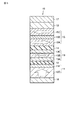
次に、本実施形態のMTJ素子10のより詳細な具体例について説明する。図2は、MTJ素子10の具体例を示す断面図である。例えば、平面形状において、フリー層13のアスペクト比は、ほぼ1に設定される。
Next, a more detailed specific example of the
基板(図示せず)側の最下層には、基本構成の結晶配向性或いは結晶性を制御するための下地層16が設けられている。この下地層16には、例えば非磁性金属層が用いられる。最上層には、基本構成を酸化及び腐食などの劣化から保護するためのキャップ層17が設けられている。キャップ層17には、例えば非磁性金属層が用いられる。
A
図3は、ピン層15の他の構成を示す断面図である。ピン層15の容易磁化方向は、膜面に対して平行である。ピン層15は、ピン層15C/中間層15B/ピン層15Aの積層構造を有している。さらに、ピン層15C上(ピン層15とキャップ層17との間)には、ピン層15Cと接するように、反強磁性層18が設けられている。ピン層15Cは、反強磁性層18と交換結合することで、膜面に対して平行に磁化の方向が固着されている。
FIG. 3 is a cross-sectional view showing another configuration of the pinned
ピン層15A及びピン層15Cの容易磁化方向は、膜面に対して平行である。また、ピン層15Aとピン層15Cとの磁化の方向は互いに反平行(反対方向)に設定され、ピン層15Aとピン層15Cとは中間層15Bを挟んで反強磁性結合している。中間層を介して互いの磁化の方向が反平行である第1の磁性層/中間層(非磁性層)/第2の磁性層の積層構造をシンセティックアンチフェロ(SAF:Synthetic Anti-Ferromagnet)構造という。このSAF構造を用いることで、ピン層15の磁化固着力が増強され、外部磁場に対する耐性及び熱的な安定性を向上させることができる。具体的には、ピン層15の磁化固着力の温度依存性が向上する。
The easy magnetization directions of the pinned
SAF構造において、第1の磁性層(ピン層15Cに対応する)の飽和磁化をMs1、膜厚をt1、第2の磁性層(ピン層15Aに対応する)の飽和磁化をMs2、膜厚をt2とすると、Ms1・t1≒Ms2・t2に設定することで、ピン層15の見かけ上の飽和磁化と磁性層膜厚との積Ms・tをほぼゼロとすることが可能となる。これにより、ピン層15は、外部磁場に反応しにくくなり、さらに外部磁場耐性を向上させることができる。
In the SAF structure, the saturation magnetization of the first magnetic layer (corresponding to the pinned
SAF構造における中間層15Bには、Ru(ルテニウム)やOs(オスミウム)などの金属材料が用いられ、その膜厚は3nm以下に設定される。これは、中間層15Bを介して十分強い反強磁性結合を得るためである。このような中間層15Bを用いることで、ピン層15の磁化固着力が増強され、外部磁場に対する耐性及び熱的な安定性が向上する。
A metal material such as Ru (ruthenium) or Os (osmium) is used for the
図4は、ピン層11の他の構成を示す断面図である。ピン層11の下(ピン層11と下地層16との間)には、ピン層11と接するように、反強磁性層19が設けられている。ピン層11は、反強磁性層19と交換結合することで、膜面に対して垂直に磁化の方向が固着されている。この構造を用いることで、ピン層11の磁化固着力が増強され、外部磁場に対する耐性及び熱的な安定性が向上する。
FIG. 4 is a cross-sectional view showing another configuration of the pinned
図5は、ピン層11の他の構成を示す断面図である。ピン層11は、ピン層11C/中間層11B/ピン層11Aの積層構造を有している。すなわち、ピン層11は、SAF構造を有している。
FIG. 5 is a cross-sectional view showing another configuration of the pinned
ピン層11A及びピン層11Cの容易磁化方向は、膜面に対して垂直である。また、ピン層11Aとピン層11Cとの磁化の方向は互いに反平行に設定され、ピン層11Aとピン層11Cとは中間層11Bを挟んで反強磁性結合している。このSAF構造を用いることで、ピン層11の磁化固着力が増強され、外部磁場に対する耐性及び熱的な安定性が向上する。なお、本構成において、ピン層11Aに接するようにピン層11Aの下に反強磁性層が設けられ、ピン層11Aと反強磁性層とが交換結合していても構わない。
The easy magnetization directions of the pinned
図6は、フリー層13及びピン層11の他の構成を示す断面図である。フリー層13は、界面フリー層13C/フリー層13B/界面フリー層13Aの積層構造を有している。このように、フリー層13Bと中間層12との間、或いは、フリー層13Bと中間層14との間に強磁性体からなる界面フリー層が挿入されることが好ましい。
FIG. 6 is a cross-sectional view showing another configuration of the
また、図6に示すように、ピン層11は、界面ピン層11E/ピン層11Dの積層構造を有している。このように、ピン層11Dと中間層12との間に強磁性体からなる界面ピン層11Eが挿入されることが好ましい。
As shown in FIG. 6, the pinned
界面ピン層及び界面フリー層は、磁気抵抗効果を増大させる効果があり、さらには、スピン注入書き込み時に書き込み電流を低減する効果がある。さらに、磁気抵抗効果を増大させる界面層には、その材料自身のバルク的な分極率が大きいことが望ましく、さらには、中間層との界面分極率が増大されるように材料を選択することが好ましい。 The interface pinned layer and the interface free layer have the effect of increasing the magnetoresistance effect, and further have the effect of reducing the write current during spin injection writing. Furthermore, it is desirable that the interface layer that increases the magnetoresistive effect has a large bulk polarizability of the material itself, and further, the material can be selected so that the interface polarizability with the intermediate layer is increased. preferable.
次に、MTJ素子10を構成する各層の材料について説明する。
Next, the material of each layer constituting the
[1] 中間層12及び中間層14に用いられる材料
本実施形態のMTJ素子10においては、中間層12には、絶縁体或いは半導体が用いられる。この場合、フリー層13/中間層12/ピン層11の構成部分でトンネル磁気抵抗効果が発現する。従って、読み出し時は、ピン層11及びフリー層13の磁化の方向が平行或いは反平行になることで、MTJ素子10の抵抗値が低抵抗或いは高抵抗となり、それぞれの状態をデータ“0”或いはデータ“1”と判別する。
[1] Materials Used for
一方で、ピン層15/中間層14/フリー層13の構成部分では、フリー層13及びピン層15の磁化の方向が直交しているためにトンネル磁気抵抗効果は発現しない。従って、中間層14には、金属導電体、絶縁体或いは半導体のどれを用いてもよい。但し、絶縁体及び半導体を用いた場合は、MTJ素子の抵抗値が上昇するので、金属導電体を用いることが好ましい。
On the other hand, in the constituent portions of the pinned
ここで、中間層14に用いられる金属導電体としては、Cu(銅)、Al(アルミニウム)、Ag(銀)及びAu(金)などが好ましい。さらには、局所的に電流密度を高めた電流集中効果を用いてスピン注入効率を向上させるために、MgO−Cu、AlOx−Cuなどの導電性金属相と絶縁相との混晶構造材料を用いることもフリー層の磁化反転電流を低減する効果がある。
Here, as a metal conductor used for the intermediate |
中間層12及び中間層14の膜厚はそれぞれ、トンネル磁気抵抗効果を利用する場合には、3nm以下となるように設定される。これは、情報の書き込み時に1×10⁵〜1×10⁷A/cm2程度のトンネル電流を流す必要があるため、MTJ素子の抵抗×面積(RA:resistance and area product)を100Ωμm2以下程度に小さくする必要があるからである。
The film thicknesses of the
中間層12及び中間層14に用いられる絶縁体としては、Al2O3(酸化アルミニウム)、MgO(酸化マグネシウム)、CaO(酸化カルシウム)、SrO(酸化ストロンチウム)、TiO(酸化チタン)、EuO(酸化ユーロビウム)、ZrO(酸化ジルコニウム)及びHfO(酸化ハフニウム)などの酸化物があげられる。また、半導体としては、Ge(ゲルマニウム)、Si(シリコン)、GaAs(ガリウムヒ素)及びInAs(インジウムヒ素)などの化合物半導体、TiO2(酸化チタン)などの酸化物半導体があげられる。MgO、CaO、SrO、TiO、及びEuOは、NaCl構造を有する。
Examples of the insulator used for the
この中でも、NaCl構造を有するMgOは、中間層12としては好ましい材料である。これは、MgOを用いた場合が最もTMR比が大きくなるからである。MgOを用いた場合、MTJ素子のRAが5Ωμm2以上1000Ωμm2以下の範囲内で100%以上のTMR比を得ることが可能である。このMgOはNaCl構造を有しており、TMR比の観点から結晶配向性としては(100)面配向が最も好ましい。また、MgO層形成時に、MgO上部或いは下部には、1nm以下のMg層を挿入することで、TMR比をさらに向上させることができる。
Among these, MgO having a NaCl structure is a preferable material for the
MgO層は、MgOターゲットを用いて希ガス(Ar(アルゴン)、Ne(ネオン)、Kr(クリプトン)或いはXe(キセノン))でのスパッタ法により形成する、或いは、Mgターゲットを用いたO2雰囲気中での酸化反応性スパッタ法により形成する。また、Mg層を成膜した後に、酸素ラジカル、酸素イオン或いはオゾンなどにより酸化することでも形成可能である。さらに、MgOを用いた分子線エピタキシー(MBE:Molecular Beam Epitaxy)法或いは電子ビーム蒸着(electron beam evaporation)法によりエピタキシャル成長させることでも形成可能である。 The MgO layer is formed by sputtering with a rare gas (Ar (argon), Ne (neon), Kr (krypton) or Xe (xenon)) using an MgO target, or an O 2 atmosphere using an Mg target. It is formed by the oxidation reactive sputtering method in the inside. Alternatively, the Mg layer can be formed by oxidizing with oxygen radicals, oxygen ions, ozone, or the like. Further, it can also be formed by epitaxial growth by molecular beam epitaxy (MBE) method using MgO or electron beam evaporation (electron beam evaporation) method.
ここで、大きいTMR比を得るためには、MgOの配向度の向上が必要である。MgOの面配向に基づいて、選択すべき下地層となる磁性層の配向性が決定される。MgOは、(100)面配向が好ましい。MgOを(100)面優先配向させるためには、その下地層(フリー層、ピン層、界面フリー層或いは界面ピン層など)は、BCC(Body-Centered Cubic)構造(100)配向面、FCC(Face-Centered Cubic)構造(100)配向面、或いは、アモルファス構造であることが好ましい。 Here, in order to obtain a large TMR ratio, it is necessary to improve the degree of orientation of MgO. Based on the plane orientation of MgO, the orientation of the magnetic layer serving as the underlayer to be selected is determined. MgO preferably has a (100) plane orientation. In order to preferentially orient MgO in the (100) plane, the underlying layer (free layer, pinned layer, interface free layer, interface pinned layer, etc.) has a BCC (Body-Centered Cubic) structure (100) orientation plane, FCC ( (Face-Centered Cubic) structure (100) Orientation plane or amorphous structure is preferable.
BCC構造の材料としては、BCC−Fe100−xCox(0≦x≦70at(原子)%)、BCC構造上にエピタキシャル成長させた1nm以下のBCC−Coなどがあげられる。或いは、BCC−Fe100−x(CoNi)x(0≦x≦70at%)などを用いてもよい。この場合、10at%以下の希薄Ni添加により10〜20%のTMR比の上昇効果が得られる。アモルファス材料としては、Co(コバルト)−Fe(鉄)−B(ホウ素)合金、Fe−Co−Zr合金などがあげられる。 Examples of the material of the BCC structure include BCC-Fe 100-x Co x (0 ≦ x ≦ 70 at (atomic%)), BCC-Co of 1 nm or less epitaxially grown on the BCC structure, and the like. Alternatively, BCC-Fe 100-x (CoNi) x (0 ≦ x ≦ 70 at%) or the like may be used. In this case, the effect of increasing the TMR ratio of 10 to 20% can be obtained by adding dilute Ni of 10 at% or less. Examples of the amorphous material include a Co (cobalt) -Fe (iron) -B (boron) alloy, an Fe—Co—Zr alloy, and the like.
[2] 垂直磁化フリー層及び垂直磁化ピン層に用いられる磁性材料
本実施形態においては、フリー層13及びピン層11に垂直磁化膜が用いられる。面内磁化フリー層を用いた場合、スイッチング磁界はMTJ素子のサイズに強く依存するが、垂直磁化フリー層を用いることにより、MTJ素子サイズの依存性が小さくなる。
[2] Magnetic Material Used for Perpendicular Magnetization Free Layer and Perpendicular Magnetization Pinned Layer In this embodiment, a perpendicular magnetization film is used for the
すなわち、面内磁化の場合、飽和磁化を利用した形状磁気異方性エネルギーにより磁化の安定性を維持させるため、素子形状及び素子サイズに依存してスイッチング磁界が変化する。一方、垂直磁化の場合、飽和磁化を小さくし、素子形状及び素子サイズに依存しない結晶磁気異方性エネルギーにより磁化の安定性を維持するために、素子形状及び素子サイズに依存してスイッチング磁界が変わることが小さくなる。従って、垂直磁化フリー層を用いることで、MTJ素子を小さくするとMTJ素子のスイッチング磁界が大きくなるという面内磁化膜を用いたMTJ素子の問題が解決され、MTJ素子の微細化には好ましい。 That is, in the case of in-plane magnetization, the switching magnetic field changes depending on the element shape and element size in order to maintain the stability of magnetization by the shape magnetic anisotropy energy using saturation magnetization. On the other hand, in the case of perpendicular magnetization, in order to reduce the saturation magnetization and maintain the stability of magnetization by the magnetocrystalline anisotropy energy independent of the element shape and element size, the switching magnetic field depends on the element shape and element size. Change will be smaller. Therefore, the use of the perpendicular magnetization free layer solves the problem of the MTJ element using the in-plane magnetization film that the switching magnetic field of the MTJ element increases when the MTJ element is reduced, which is preferable for miniaturization of the MTJ element.
本実施形態のMTJ素子10に用いられる垂直磁化膜としては、Fe(鉄)、Co(コバルト)、Ni(ニッケル)及びMn(マンガン)のうち少なくとも1種類以上と、Pt(白金)、Pd(パラジウム)、Ir(イリジウム)、Rh(ロジウム)、Os(オスミウム)、Au(金)、Ag(銀)、Cu(銅)、及びCr(クロム)のうち少なくとも1種類以上とを含むことを基本とする。さらには、飽和磁化の調整、結晶磁気異方性エネルギーの制御、結晶粒径及び結晶粒間結合の調整をするために、B(ホウ素)、C(炭素)、Si(シリコン)、Al(アルミニウム)、Mg(マグネシウム)、Ta(タンタル)、Zr(ジルコニウム)、Ti(チタン)、Hf(ハフニウム)、Y(イットリウム)、及び希土類元素から選ばれる少なくとも1種類以上の元素を添加してもよい。これらの元素の添加により、飽和磁化Ms及び結晶磁気異方性エネルギーKuを、垂直磁化を損なわせることなく低下させることが可能となり、結晶粒の分断及び微細化を促進できる。
As the perpendicular magnetization film used for the
Coを主成分とする材料として、具体的には、HCP(Hexagonal Closest Packing)構造を有するCo−Cr−Pt合金、Co−Cr−Ta合金、或いはCo−Cr−Pt−Ta合金などがあげられる。これらは、各元素の組成を調整することにより、1×10⁵以上1×10⁷erg/cc未満の範囲内で結晶磁気異方性エネルギーを調整することが可能である。これらの材料を基板に近い側のピン層に用いる場合、下地層としてHCP構造を有するRuを用いることが好ましい。 Specific examples of the Co-based material include a Co—Cr—Pt alloy, a Co—Cr—Ta alloy, and a Co—Cr—Pt—Ta alloy having an HCP (Hexagonal Closest Packing) structure. . By adjusting the composition of each element, it is possible to adjust the magnetocrystalline anisotropy energy within the range of 1 × 10 5 or more and less than 1 × 10 7 erg / cc. When these materials are used for the pinned layer close to the substrate, Ru having an HCP structure is preferably used as the underlayer.
Co−Pt合金は、Co50Pt50(at%)付近の組成域において、L10−CoPt規則合金を形成する。この規則合金は、FCT(Face-Centered Tetragonal)構造を有する。中間層12としてMgO(100)を用いる場合、(001)面配向したFCT−CoPt規則合金は、中間層12との界面ミスフィットも小さくできるので好ましい。また、中間層とフリー層(或いはピン層)との間に界面層を挿入した場合でも、界面層を(100)面配向しやすくできる。
The Co—Pt alloy forms an L1 0 -CoPt ordered alloy in the composition range near Co 50 Pt 50 (at%). This ordered alloy has an FCT (Face-Centered Tetragonal) structure. When MgO (100) is used as the
Feを主成分とする材料として、具体的には、Fe−Pt合金或いはFe−Pd合金があげられる。中でも、Fe−Pt合金は、組成がFe50Pt50(at%)において規則化し、FCT構造を基本構造とするL10構造を有する。また、Fe−Pt合金は、組成がFe75Pt25(at%)において規則化し、FCT構造を基本構造とするL12構造(Fe3Pt構造)を有する。これにより、1×10⁷erg/cc以上の大きな結晶磁気異方性エネルギーを発現することができる。 Specific examples of the material mainly containing Fe include an Fe—Pt alloy and an Fe—Pd alloy. Among them, Fe-Pt alloy composition is ordered in Fe 50 Pt 50 (at%) , having an L1 0 structure as a basic structure FCT structure. Further, Fe-Pt alloy composition is ordered in Fe 75 Pt 25 (at%) , having an L1 2 structure as a basic structure FCT structures (Fe 3 Pt structure). Thereby, a large magnetocrystalline anisotropy energy of 1 × 10 7 erg / cc or more can be expressed.
Fe50Pt50合金は、L10構造に規則化する前は、FCC構造を有する。この場合の結晶磁気異方性エネルギーは、1×10⁶erg/cc程度である。従って、アニール温度、組成の調整、積層構成による規則度の制御、及び添加物の添加により、5×105erg/cc以上5×108erg/cc以下の範囲内で結晶磁気異方性エネルギーを調整することができる。また、飽和磁化も添加前はおおよそ800〜1100emu/ccであるが、800emu/cc以下に低減することが可能である。これは、フリー層に使う場合において、電流密度Jcの低威という点で好ましい。 Fe 50 Pt 50 alloy, prior to ordering the L1 0 structure and has a FCC structure. In this case, the magnetocrystalline anisotropy energy is about 1 × 10 6 erg / cc. Accordingly, the magnetocrystalline anisotropy energy is within the range of 5 × 10 5 erg / cc to 5 × 10 8 erg / cc by adjusting the annealing temperature, adjusting the composition, controlling the degree of order by the laminated structure, and adding the additive. Can be adjusted. Also, the saturation magnetization is approximately 800 to 1100 emu / cc before addition, but can be reduced to 800 emu / cc or less. This is preferable in terms of low current density Jc when used for the free layer.
具体的には、L10規則構造を有するFe−Pt合金にCu(銅)、Ti(チタン)、V(バナジウム)、Mn(マンガン)、或いはCr(クロム)などを30at%以下の範囲で添加することで、Fe−Pt合金の飽和磁化(Ms)、及び結晶磁気異方性エネルギー(Ku)を制御することが可能である。また、Vに関しては、スピン注入磁化反転において重要なダンピング定数(磁化制動定数)を下げる効果があり、反転電流を低減する効果もある。 Specifically, added in Fe-Pt alloy Cu (copper), Ti (titanium), V (vanadium), Mn (manganese), or Cr (chromium) range below 30 at%, such as having an L1 0 ordered structure By doing so, it is possible to control the saturation magnetization (Ms) and the magnetocrystalline anisotropy energy (Ku) of the Fe—Pt alloy. Further, with respect to V, there is an effect of lowering a damping constant (magnetization braking constant) that is important in spin injection magnetization reversal, and also an effect of reducing reversal current.
L10構造或いはL12構造に規則化したFe−Pt合金はFCT構造を有し、規則化する前はFCC構造を有する。従って、MgO(100)とは非常に整合性がよい。具体的には、MgO(100)面上に(100)面配向したBCC−Feを成長させ、その上にPt(100)を積層することで、MgO(100)上に(100)面優先配向成長したL10構造或いはL12構造のFe−Pt規則合金を形成することが可能である。また、Fe−Pt規則合金とMgO(100)との間にBCC−Crを形成すると、さらにFe−Pt規則合金の(100)面配向が優先的となり望ましい。 L1 0 structure or Fe-Pt alloy ordered to L1 2 structure has a FCT structure, prior to ordering has a FCC structure. Therefore, it is very consistent with MgO (100). Specifically, a (100) plane-oriented orientation is formed on MgO (100) by growing (100) -oriented BCC-Fe on the MgO (100) plane and laminating Pt (100) thereon. It is possible to form an Fe-Pt ordered alloy having a grown L1 0 structure or L1 2 structure. Further, when BCC-Cr is formed between the Fe—Pt ordered alloy and MgO (100), the (100) plane orientation of the Fe—Pt ordered alloy is more preferred.
また、L10構造或いはL12構造のFe−Pt規則合金を形成する場合、[Fe/Pt]n(nは1以上の整数)の多層構造を形成すると理想的な規則に近いL10構造或いはL12構造のFe−Pt規則合金を形成できる。この場合、Fe及びPtの膜厚は、0.1nm以上3nm以下となるように設定されることが望ましい。これは、均一な組成状態を作り出すためには必須であり、それにより、L10構造或いはL12構造のFe−Pt合金の規則化の場合、FCC構造からFCT構造へのマルテンサイト変態(martensitic transformation)を伴うため、この変態が促進されるので重要である。 Further, when forming an Fe—Pt ordered alloy having an L1 0 structure or an L1 2 structure, if a multilayer structure of [Fe / Pt] n (n is an integer of 1 or more) is formed, the L1 0 structure or L1 2 structure Fe-Pt ordered alloy can be formed. In this case, the film thicknesses of Fe and Pt are desirably set to be 0.1 nm or more and 3 nm or less. This is to create a uniform composition state is essential, thereby, when the ordering of the Fe-Pt alloy of the L1 0 structure or L1 2 structure, martensitic transformation from FCC structure to FCT structure (martensitic transformation ) Is important because this transformation is promoted.
また、L10構造或いはL12構造のFe−Pt合金の規則化温度は500度以上と高く、耐熱性に優れている。この点は、後工程でのアニール処理に対する耐性があることとなり、非常に好ましい。また、上述したCuやPdなどの30at%以下の範囲での添加元素により、その規則化温度を低下させることが可能である。 Further, ordering temperature of L1 0 structure or L1 2 structure Fe-Pt alloys is as high as more than 500 degrees, is excellent in heat resistance. This point is very preferable because it has resistance to annealing treatment in a later step. Further, the ordering temperature can be lowered by the additive element in the range of 30 at% or less such as Cu and Pd described above.
本実施形態のMTJ素子10に用いられる他の垂直磁化膜としては、Fe、Co、Ni、Mn、Cr及び希土類元素のうち少なくとも1種類以上を含むフェリ磁性体があげられる。希土類元素としては、La(ランタン)、Ce(セリウム)、Pr(プラセオジウム)、Nd(ネオジム)、Pm(ブロメチウム)、Sm(サマリウム)、Eu、Gd(ガドリニウム)、Tb(テルビウム)、Dy(ジスプロシウム)、Ho(ホルミウム)、Er(エルビウム)、Tm(ツリウム)、Yb(イッテルビウム)、及びLu(ルテチウム)などがあげられる。
Examples of other perpendicular magnetization films used in the
希土類元素を含むフェリ磁性体は、アモルファス構造を有する。このフェリ磁性体は、組成の調整により、飽和磁化を400emu/cc以下に低減し、かつ、結晶磁気異方性エネルギーを1×106erg/cc以上に向上させることが可能である。 Ferrimagnetic materials containing rare earth elements have an amorphous structure. This ferrimagnetic material can reduce the saturation magnetization to 400 emu / cc or less and improve the magnetocrystalline anisotropy energy to 1 × 10 6 erg / cc or more by adjusting the composition.
さらに、本実施形態のMTJ素子10に用いられる垂直磁化膜としては、金属磁性相と絶縁相との混晶からなる強磁性体を用いてもよい。この場合、金属磁性相は、Fe、Co、Ni、及びMnのうち少なくとも1種類以上と、Pt、Pd、Ir、Rh、Os、Au、Ag、Cu、Cr、Ta、及び希土類元素のうち少なくとも1種類以上とを含む強磁性体から構成される。絶縁相は、B、C、Si、Al、Mg、Ta、Cr、Zr、Ti、Hf、Y、及び希土類元素から選ばれる少なくとも1種類以上の元素を含む酸化物、窒化物、及び酸窒化物から構成される。
Further, as the perpendicular magnetization film used in the
金属磁性相と絶縁相との混晶からなる強磁性体は、導電性を有する金属磁性体部と非導電性の絶縁体部とに分離しているために、金属磁性体部に電流が集中して通電面積が小さくなり、局所的な電流密度が上昇する。これにより、実質的に必要となる反転電流が小さくなる効果を有する。 Ferromagnetic material consisting of mixed crystal of metal magnetic phase and insulating phase is separated into conductive metal magnetic part and non-conductive insulator part, so current concentrates on metal magnetic part As a result, the current-carrying area is reduced and the local current density is increased. This has the effect of reducing the required reversal current substantially.
このような効果を得るためには、結晶性を制御する必要がある。2相分離構造としては、グラニュラー(結晶粒分散)型構造、アイランド(島状)型構造、及びコラムナー(柱状)型構造がある。コラムナー型構造の場合は、磁性層中で金属磁性体部が上下に貫通しているので、電流狭窄効果が得られやすい。グラニュラー型構造及びアイランド型構造の場合は、電流はもっともトンネル障壁が小さいパスを通電することとなるので、コラムナー型構造と同様に電流狭窄効果が得られる。 In order to obtain such an effect, it is necessary to control the crystallinity. As the two-phase separation structure, there are a granular (crystal grain dispersion) type structure, an island (island shape) type structure, and a columner (columnar type) type structure. In the case of the columnar structure, since the metal magnetic body portion vertically penetrates in the magnetic layer, a current confinement effect is easily obtained. In the case of the granular type structure and the island type structure, since the current flows through the path having the smallest tunnel barrier, the current confinement effect can be obtained as in the columnar type structure.
その他、本実施形態のMTJ素子10に用いられる垂直磁化膜としては、Mn系強磁性合金、或いは、Cr系強磁性合金があげられる。Mn系強磁性合金としては、Mn−Al合金、Mn−Au合金、Mn−Zn合金、Mn−Ga合金、Mn−Ir合金、及びMn−Pt3合金などがあり、これらは、規則格子を有する特徴がある。また、Cr系磁性合金としては、Cr−Pt3合金などがあげられる。これは、L10規則格子を有し、フェリ磁性体の特性を有する。
In addition, examples of the perpendicular magnetization film used in the
[3] 面内磁化ピン層に用いられる磁性材料
本実施形態においては、磁化の方向がピン層11に直交しているピン層15には、面内磁化膜が用いられる。
[3] Magnetic Material Used for In-Plane Magnetized Pinned Layer In the present embodiment, an in-plane magnetized film is used for the pinned
本実施形態のMTJ素子10に用いられる面内磁化膜としては、Fe、Co、Ni、Mn、及びCrのうち少なくとも1種類以上を含む強磁性体が用いられる。Fe、Co、及びNiを主成分とする材料として、具体的には、FCC構造或いはBCC構造を有するFexCoyNiz合金(x≧0、y≧0、z≧0、x+y+z=1)があげられる。
As the in-plane magnetization film used in the
ピン層に用いられる材料としては、分極率が大きく、原理的に100%分極率を実現できるハーフメタル的な材料が好ましい。 The material used for the pinned layer is preferably a half-metal material having a high polarizability and capable of realizing 100% polarizability in principle.
Mnを含む材料としては、Mn系強磁性ホイスラー合金がハーフメタル材料としてあげられる。ここで、Mn系強磁性ホイスラー合金は、A2MnXで表される規則格子を有する体心立方晶系(body-centered cubic system)合金である。A元素は、Cu、Au、Pd、Ni、及びCoから選択される材料である。X元素は、Al(アルミニウム)、In(インジウム)、Sn(すず)、Ga(ガリウム)、Ge(ゲルマニウム)、Sb(アンチモン)、及びSi(シリコン)から選択される材料である。ホイスラー合金のうち、BCC構造を有するCo2MnAl合金などは、BCC(100)面配向させることにより、MgO(100)との整合性が良好となる。 An example of the material containing Mn is a Mn-based ferromagnetic Heusler alloy as a half-metal material. Here, the Mn-based ferromagnetic Heusler alloy is a body-centered cubic system alloy having an ordered lattice represented by A 2 MnX. The element A is a material selected from Cu, Au, Pd, Ni, and Co. The X element is a material selected from Al (aluminum), In (indium), Sn (tin), Ga (gallium), Ge (germanium), Sb (antimony), and Si (silicon). Among Heusler alloys, a Co 2 MnAl alloy having a BCC structure or the like has good consistency with MgO (100) by being oriented in the BCC (100) plane.
ピン層中の強磁性層の膜厚は、1nm以上が必要である。なぜなら、上記の膜厚未満では、強磁性層が連続膜にならず、磁性層としての特性が十分に発揮されず、十分な磁気抵抗効果比(TMR比或いはGMR(Giant Magnetoresistive)比)が得られない。また、最大膜厚は、3nm以下であることが望ましい。これは、膜厚が3nmを超えると、コヒーレントなスピンの歳差運動長さをはるかに越えてしまうために、スピン注入磁化反転に必要な電流閾値が大幅に大きくなってしまうからである。 The film thickness of the ferromagnetic layer in the pinned layer needs to be 1 nm or more. This is because if the thickness is less than the above-mentioned thickness, the ferromagnetic layer does not become a continuous film, and the characteristics as a magnetic layer are not sufficiently exhibited, and a sufficient magnetoresistance effect ratio (TMR ratio or GMR (Giant Magnetoresistive) ratio) is obtained. I can't. The maximum film thickness is desirably 3 nm or less. This is because when the film thickness exceeds 3 nm, the current threshold necessary for spin injection magnetization reversal is significantly increased because the coherent spin precession length is far exceeded.
また、上述した面内磁化ピン層がMgOバリア層の下地層となる場合、組成式FexCoyNiz合金(x≧0、y≧0、z≧0、x+y+z=1)で表される材料において、(100)面配向を有し、BCC構造を有することが好ましい。さらには、組成式FexCoyNiz合金(x≧0、y≧0、z≧0、x+y+z=1)で表される材料にB、C、Nなどを30at%以下の濃度で添加し、アモルファス構造にすることも好ましい。これは、アモルファス構造を有する膜上では、MgO膜は(100)面を優先配向しやすいからである。 Further, when the above-described in-plane magnetization pinned layer is an underlayer of the MgO barrier layer, it is expressed by a composition formula Fe x Co y N z alloy (x ≧ 0, y ≧ 0, z ≧ 0, x + y + z = 1). The material preferably has a (100) plane orientation and a BCC structure. Furthermore, added to the material represented by the composition formula Fe x Co y Ni z alloy (x ≧ 0, y ≧ 0 , z ≧ 0, x + y + z = 1) B, C, N and at a concentration of less than 30 at% It is also preferable to use an amorphous structure. This is because the MgO film tends to preferentially orient the (100) plane on the film having an amorphous structure.
[4] 界面フリー層及び界面ピン層に用いられる材料
図6に示した界面ピン層及び界面フリー層(以下、両方を指して界面層)は、磁気抵抗効果を増大させる効果があり、さらには、スピン注入書き込み時に書き込み電流を低減する効果がある。磁気抵抗効果を増大させる界面層は、その材料自身のバルク的な分極率が大きいことが望ましく、さらには、中間層との界面分極率が増大されるように材料を選択することが好ましい。
[4] Materials used for interface free layer and interface pinned layer The interface pinned layer and interface free layer (hereinafter referred to as interface layer) shown in FIG. 6 have the effect of increasing the magnetoresistance effect, and This has the effect of reducing the write current during spin injection writing. The interface layer that increases the magnetoresistive effect desirably has a large bulk polarizability of the material itself, and further, the material is preferably selected so that the interface polarizability with the intermediate layer is increased.
本実施形態のMTJ素子10に用いられる界面層としては、Fe、Co、Ni、Mn、及びCrのうち少なくとも1種類以上を含む強磁性体が用いられる。Fe、Co、及びNiを主成分とする材料として、具体的には、FCC構造或いはBCC構造を有するFexCoyNiz合金(x≧0、y≧0、z≧0、x+y+z=1)があげられる。また、上記のFe−Co−Ni合金の飽和磁化(Ms)を低減するために、(FexCoyNiz)100−aXa合金(x≧0、y≧0、z≧0、x+y+z=1、a(at%)>0、Xは添加元素)も好ましい。飽和磁化(Ms)を低減することにより、反転電流を大幅に低減することが可能となる。FeCoNiが50at%以上であることが好ましいが、これはx+y+z>50at%である場合、バリア層界面でのFeCoNi磁性層の被覆率が50%以上になるために、TMR現象効果を抑制できるからである。
As the interface layer used in the
BCC構造を崩さずに添加することができ、かつ、飽和磁化(Ms)を低減できる添加物、すなわち、置換型で固溶できる全率固溶体或いはある程度固溶源を有する添加物としては、V(バナジウム)、Nb(ニオブ)、Ta(タンタル)、W(タングステン)、Cr(クロム)、Mo(モリブデン)、Si(シリコン)、Ga(ガリウム)、及びGe(ゲルマニウム)などがあげられる。この中でも、Vは、ダンピング定数(磁化制動定数)を低減する効果もあり有効である。 As an additive that can be added without breaking the BCC structure and can reduce the saturation magnetization (Ms), that is, an all-solid solution that can be dissolved in a substitution type or an additive having a solid solution source to some extent, V ( Examples include vanadium), Nb (niobium), Ta (tantalum), W (tungsten), Cr (chromium), Mo (molybdenum), Si (silicon), Ga (gallium), and Ge (germanium). Among these, V is effective because it has an effect of reducing a damping constant (magnetization braking constant).
また、B、C及びNなどの侵入型元素を添加する、或いは、ほとんど固溶源を持たないZr、Ta、Ti、Hf、Y、及び希土類元素などを添加することにより、結晶構造をアモルファス構造に変えることで飽和磁化(Ms)を低減できる。このような材料として、例えば、アモルファス構造を有する(FexCoyNiz)100−bXb合金(x≧0、y≧0、z≧0、x+y+z=1、b(at%)>0、XはB、C、N、Zr、Ta、Ti、Hf、Y、及び希土類元素などの添加元素)があげられる。但し、ある程度のTMR比を得るためには、部分的に、すなわち、MgOとの界面において再結晶化を促進させることが重要となる。 Further, by adding interstitial elements such as B, C, and N, or adding Zr, Ta, Ti, Hf, Y, rare earth elements and the like that have almost no solid solution source, the crystal structure is made amorphous. By changing to, saturation magnetization (Ms) can be reduced. As such a material, for example, has an amorphous structure (Fe x Co y Ni z) 100-b X b alloy (x ≧ 0, y ≧ 0 , z ≧ 0, x + y + z = 1, b (at%)> 0 , X includes B, C, N, Zr, Ta, Ti, Hf, Y, and additional elements such as rare earth elements). However, in order to obtain a certain TMR ratio, it is important to promote recrystallization partially, that is, at the interface with MgO.
Mnを含む材料としては、Mn系強磁性ホイスラー合金があげられる。ここで、Mn系強磁性ホイスラー合金は、A2MnXで表される規則格子を有する体心立方晶系合金である。A元素は、Cu、Au、Pd、Ni、及びCoから選択される材料である。X元素は、Al、In、Sn、Ga、Ge、Sb、及びSiから選択される材料である。ホイスラー合金のうち、BCC構造を有するCo2MnAl合金などは、BCC(100)面配向させることにより、MgO(100)との整合性が良好となる。Mn系ホイスラー合金は、ハーフメタル的な伝導特性を示す場合がある。 An example of the material containing Mn is a Mn-based ferromagnetic Heusler alloy. Here, the Mn-based ferromagnetic Heusler alloy is a body-centered cubic alloy having an ordered lattice represented by A 2 MnX. The element A is a material selected from Cu, Au, Pd, Ni, and Co. The X element is a material selected from Al, In, Sn, Ga, Ge, Sb, and Si. Among Heusler alloys, a Co 2 MnAl alloy having a BCC structure or the like has good consistency with MgO (100) by being oriented in the BCC (100) plane. An Mn-based Heusler alloy may exhibit half-metal conduction characteristics.
また、酸化物材料を用いることもできる。酸化物材料としては、Fe2O3などのハーフメタルなどが界面層として適用可能である。 An oxide material can also be used. As the oxide material, a half metal such as Fe 2 O 3 can be used as the interface layer.
フリー層或いはピン層などの金属層の上に形成される界面層の最小膜厚としては、0.5nm以上が必要であり、絶縁層或いは半導体層上に形成される界面層の最小膜厚としても、0.5nm以上が必要である。なぜなら、上記の膜厚未満では、界面層が連続膜にならず、界面フリー層或いは界面ピン層としての特性が十分に発揮されず、十分な磁気抵抗効果比(TMR比或いはGMR比)が得られない。また、最大膜厚は、5nm以下であることが望ましい。これは、膜厚が5nmを超えると、コヒーレントなスピンの歳差運動長さをはるかに越えてしまうために、スピン注入磁化反転に必要な電流閾値が大幅に大きくなってしまうからである。 As the minimum film thickness of the interface layer formed on the metal layer such as the free layer or the pinned layer, 0.5 nm or more is necessary. As the minimum film thickness of the interface layer formed on the insulating layer or the semiconductor layer, However, 0.5 nm or more is necessary. This is because if the thickness is less than the above-mentioned thickness, the interface layer does not become a continuous film, and the characteristics as the interface free layer or the interface pinned layer are not sufficiently exhibited, and a sufficient magnetoresistance effect ratio (TMR ratio or GMR ratio) is obtained. I can't. The maximum film thickness is desirably 5 nm or less. This is because if the film thickness exceeds 5 nm, the current threshold required for spin injection magnetization reversal becomes significantly large because the precession length of the coherent spin is far exceeded.
以上詳述したように本実施形態によれば、互いに垂直な磁化の方向を有する2つのピン層をデュアルピン層構造で有することにより、フリー層13へのスピン注入効率を向上させることができる。これにより、MTJ素子10のスイッチング速度を向上させることができる。さらに、スピン注入効率が向上する結果、磁化反転に必要な書き込み電流を低減することが可能となる。
As described in detail above, according to the present embodiment, the efficiency of spin injection into the
また、フリー層13とピン層11との磁化の方向は互いに平行に設定され、一方、フリー層13とピン層15との磁化の方向は互いに直交するように設定されている。従って、中間層12では磁気抵抗効果が発現するが、中間層14では磁気抵抗効果が発現しない。これにより、情報の読み出し時において、MTJ素子10のTMR比をより大きくすることができる。
Further, the magnetization directions of the
また、磁気抵抗効果が発現しない中間層14に金属等の導電体を用いることが可能となる。これにより、MTJ素子10の抵抗値を低減することができる。
In addition, a conductor such as a metal can be used for the
また、フリー層13に垂直磁化膜を用いている。すなわち、フリー層13が熱的に安定するのに必要な異方性磁界(Hk)は、結晶磁気異方性エネルギーにより賄われる。これにより、フリー層13のアスペクト比を小さくできるため、MTJ素子サイズを微細化することが可能である。
In addition, a perpendicular magnetization film is used for the
また、フリー層13と中間層12、或いは、フリー層13と中間層14との間に強磁性体からなる界面フリー層を挿入している。さらに、ピン層11と中間層12との間に強磁性体からなる界面ピン層を挿入している。これらの界面フリー層及び界面ピン層に材料自身のバルク的な分極率が大きい材料を用いることで、磁気抵抗効果を増大させることができ、さらには、書き込み時の書き込み電流を低減することができる。
An interfacial free layer made of a ferromagnetic material is inserted between the
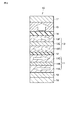
MTJ素子に用いられるTMR膜のより具体的な積層構造としては、下記のようなものがあげられる。なお、実施例1乃至実施例3において、各層の後に記載した数値は、膜厚を示している。 As a more specific laminated structure of the TMR film used for the MTJ element, the following can be cited. In Examples 1 to 3, the numerical values described after each layer indicate the film thickness.
(実施例1)
Ta5/PtMn15/CoFe2.5/Ru0.85/CoFe2.5/Cu3(中間層14)/CoFeB0.5/FePt(L10)2/Fe0.5/MgO0.75(中間層12)/CoFeB1/FePt(L10)10/Pt5/Cr20/MgO2/CoFeB2/Ta5//基板
(実施例2)
Ta5/IrMn10/CoFe2.5/Ru0.85/CoFe2.5/Cu3(中間層14)/CoFeB0.5/CoFeTb3/CoFeB0.75/MgO0.75(中間層12)/CoFeB2/CoFeTb30/Ru5/Ta5//基板
(実施例3)
Ta5/IrMn10/CoFe2.5/Ru0.85/CoFe2.5/Cu3(中間層14)/CoFeB0.5/CoPt3/CoFeB0.5/MgO0.75(中間層12)/CoFeB2/CoPt20/Ru10/Ta5//基板
実施例1及び実施例3においては、面内方向磁場中かつ真空中で270℃のアニールを施した。これらのMTJ膜を用いて、四端子測定が可能なMTJ素子を作成し、スピン注入磁化反転に必要な電流密度Jcを評価した。測定はパルス幅が1m秒で行った。MTJ素子サイズはおおよそ100nm×100nmであり、アスペクト比は1である。また、MTJ素子の抵抗×面積(RA)がそれぞれ15Ωμm2になるように、MgO膜厚を調整した。
(Example 1)
Ta5 / PtMn15 / CoFe2.5 / Ru0.85 / CoFe2.5 / Cu3 (intermediate layer 14) /CoFeB0.5/FePt (L1 0 ) 2 / Fe0.5 / MgO0.75 (intermediate layer 12) / CoFeB1 / FePt (L1 0 ) 10 / Pt5 / Cr20 / MgO2 / CoFeB2 / Ta5 // substrate (Example 2)
Ta5 / IrMn10 / CoFe2.5 / Ru0.85 / CoFe2.5 / Cu3 (intermediate layer 14) /CoFeB0.5/CoFeTb3/CoFeB0.75/MgO0.75 (intermediate layer 12) / CoFeB2 / CoFeTb30 / Ru5 / Ta5 / / Substrate (Example 3)
Ta5 / IrMn10 / CoFe2.5 / Ru0.85 / CoFe2.5 / Cu3 (intermediate layer 14) /CoFeB0.5/CoPt3/CoFeB0.5/MgO0.75 (intermediate layer 12) / CoFeB2 / CoPt20 / Ru10 / Ta5 / / Substrate In Example 1 and Example 3, annealing was performed at 270 ° C. in an in-plane magnetic field and in a vacuum. Using these MTJ films, MTJ elements capable of four-terminal measurement were prepared, and the current density Jc required for spin injection magnetization reversal was evaluated. The measurement was performed with a pulse width of 1 ms. The MTJ element size is approximately 100 nm × 100 nm and the aspect ratio is 1. Further, the MgO film thickness was adjusted so that the resistance × area (RA) of the MTJ element was 15 Ωμm 2 .
それぞれの実施例において、中間層14の上に面内磁化ピン層がない場合の比較例と比較した結果、電流密度Jcはそれぞれ、10%から30%程度の低減効果が得られた。また、それぞれの実施例において中間層14にCuを用いたため、抵抗×面積(RA)の上昇はほとんど見られず、TMR比の大きな劣化も測定されなかった。
In each example, as a result of comparison with a comparative example in which no in-plane magnetization pinned layer was provided on the
(第2の実施形態)
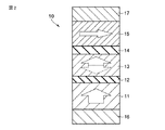
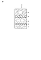
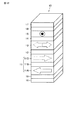
第2の実施形態は、フリー層13に面内磁化膜を用いてMTJ素子10を構成するようにしている。図7は、本発明の第2の実施形態に係るMTJ素子10の構成を示す断面図である。図7は、本実施形態のMTJ素子10の基本構成を示している。
(Second Embodiment)
In the second embodiment, the
MTJ素子10は、第1のピン層11、第1の中間層12、フリー層13、第2の中間層14、第2のピン層15が順に積層された積層構造を有している。なお、この基本構成は、積層順序が逆転していても構わない。
The
ピン層11及びフリー層13の容易磁化方向は膜面に対して平行であり、ピン層15の容易磁化方向は膜面に対して垂直である。すなわち、ピン層11とピン層15とは、容易磁化方向が互いに直交している。従って、磁化配列が平行となるフリー層13とピン層11との間では中間層12を介して磁気抵抗効果が発現するが、磁化配列が垂直となるフリー層13とピン層15との間では中間層14を介した磁気抵抗効果は発現しない。
The easy magnetization directions of the pinned
図8は、MTJ素子10の具体例を示す断面図である。図7に示した基本構成の最上層及び最下層にそれぞれ、キャップ層17及び下地層16が設けられている。ピン層11は、ピン層11C/中間層11B/ピン層11Aの積層構造を有している。すなわち、ピン層11は、SAF構造を有している。
FIG. 8 is a cross-sectional view showing a specific example of the
ピン層11A及びピン層11Cの容易磁化方向は、膜面に対して平行である。また、ピン層11Aとピン層11Cとの磁化の方向は互いに反平行に設定され、ピン層11Aとピン層11Cとは中間層11Bを挟んで反強磁性結合している。SAF構造における中間層には、RuやOsなどの金属材料が用いられ、その膜厚は3nm以下に設定される。これは、中間層を介して十分強い反強磁性結合を得るためである。
The easy magnetization directions of the pinned
さらに、ピン層11Aの下(ピン層11Aと下地層16との間)には、ピン層11Aと接するように、反強磁性層19が設けられている。ピン層11Aは、反強磁性層19と交換結合することで、膜面に対して平行に磁化の方向が固着されている。
Further, an
この構造を用いることで、ピン層11の磁化固着力が増強され、外部磁場に対する耐性及び熱的な安定性を向上させることができる。また、外部磁場に対する耐性を向上させるために、ピン層11の見かけ上の飽和磁化と磁性層膜厚との積Ms・tをほぼゼロとなるように設定することが好ましい。
By using this structure, the magnetization pinning force of the pinned
図9は、フリー層13の他の構成を示す断面図である。フリー層13は、フリー層13F/中間層13E/フリー層13Dの積層構造を有している。すなわち、フリー層13は、SAF構造を有している。フリー層13D及びフリー層13Fの容易磁化方向は、膜面に対して平行である。また、フリー層13Dとフリー層13Fとの磁化の方向は互いに反平行に設定され、フリー層13Dとフリー層13Fとは中間層13Eを挟んで反強磁性結合している。SAFフリー層の場合、磁化反転時の歳差運動を促進する効果がある。SAFフリー層では、見かけ上のネットMsはゼロに設定できるために、膜面垂直方向において、反磁界を抑制できる。従って、フリー層13の歳差運動を促進し、スピン注入磁化反転を低減する効果がある。
FIG. 9 is a cross-sectional view showing another configuration of the
このようにしてMTJ素子10を構成した場合でも、上記第1の実施形態と同様の効果を得ることができる。なお、上記第1の実施形態で示したように、フリー層13及びピン層11に界面層を挿入してもよい。
Even when the
さらに、ピン層15は、中間層14が薄い場合においては、フリー層13の磁化反転時の歳差運動を容易にする効果を有する。面内磁化膜におけるスピン注入磁化反転において、膜面垂直方向の反磁界は磁化の歳差運動を阻害し、スピン注入磁化反転電流を上昇させる要因となっている。この時の膜面垂直方向における反磁界とは、フリー層13の膜面に磁荷が発生することにより生じる。従って、膜面に発生する磁荷をキャンセルすれば、膜面垂直方向の反磁界が低下し、フリー層13の磁化は歳差運動をしやすくなる。結果的に、スピン注入磁化反転電流を低下させることが可能である。
Furthermore, the pinned
本実施形態のMTJ素子10の場合、中間層14を介して形成されているピン層15は、垂直磁化であり、膜面に磁荷を出している。従って、フリー層13が歳差運動する際には、フリー層13の膜面の磁荷をキャンセルする効果が働く。この効果を最大限に発揮するためには、中間層14はなるべく薄い方が好ましく、1nm以下であることが好ましい。1nmを超える厚さを有する中間層14の場合、ピン層15の磁化の影響は距離に反比例するために、かなり部分の漏洩磁界が減衰してしまう。歳差運動を促進する効果だけを得る場合においては、中間層14は無い方が良い。ただし、この場合は、垂直磁化膜の部分は、ピン層としての機能が失われ、フリー層13の一部として振舞うことになる。すなわち、面内磁化方向と垂直磁化方向の2方向の異方性を有するフリー層13となる。
In the case of the
本実施形態のフリー層13には、Fe−Co−Ni合金が主として用いられる。また、Fe−Co−Ni合金の飽和磁化(Ms)を低減するために、(FexCoyNiz)100−aXa合金(x≧0、y≧0、z≧0、x+y+z=1、a(at%)>0、Xは添加元素)も好ましい。飽和磁化(Ms)を低減することにより、反転電流を大幅に低減することが可能となる。
For the
BCC構造を崩さずに添加することができ、かつ、飽和磁化(Ms)を低減できる添加物、すなわち、置換型で固溶できる全率固溶体或いはある程度固溶源を有する添加物としては、V、Nb、Ta、W、Cr、Mo、Si、Ga及びGeなどがあげられる。この中でも、Vは、ダンピング定数(磁化制動定数)を低減する効果もあり有効である。 As an additive that can be added without breaking the BCC structure and that can reduce saturation magnetization (Ms), that is, a complete solid solution that can be dissolved in a substitutional form or an additive that has a solid solution source to some extent, V, Examples thereof include Nb, Ta, W, Cr, Mo, Si, Ga, and Ge. Among these, V is effective because it has an effect of reducing a damping constant (magnetization braking constant).
また、B、C及びNなどの侵入型元素を添加する、或いは、ほとんど固溶源を持たないZr、Ta、Ti、Hf、Y及び希土類元素などを添加することにより、結晶構造をアモルファス構造に変えることで飽和磁化(Ms)を低減できる。このような材料として、例えば、アモルファス構造を有する(FexCoyNiz)100−bXb合金(x≧0、y≧0、z≧0、x+y+z=1、b(at%)>0、XはB、C、N、Zr、Ta、Ti、Hf、Y、及び希土類元素などの添加元素)があげられる。 Further, by adding interstitial elements such as B, C and N, or adding Zr, Ta, Ti, Hf, Y and rare earth elements which have almost no solid solution source, the crystal structure is changed to an amorphous structure. By changing the saturation magnetization (Ms) can be reduced. As such a material, for example, has an amorphous structure (Fe x Co y Ni z) 100-b X b alloy (x ≧ 0, y ≧ 0 , z ≧ 0, x + y + z = 1, b (at%)> 0 , X includes B, C, N, Zr, Ta, Ti, Hf, Y, and additional elements such as rare earth elements).
Mnを含む材料としては、Mn系強磁性ホイスラー合金があげられる。ホイスラー合金は、ハーフメタル的な伝導特性を示す材料である。ここで、Mn系強磁性ホイスラー合金は、A2MnXで表される規則格子を有する体心立方晶系(body-centered cubic system)合金である。A元素は、Cu、Au、Pd、Ni、及びCoから選択される材料である。X元素は、Al、In、Sn、Ga、Ge、Sb、及びSiから選択される材料である。ホイスラー合金のうち、BCC構造を有するCo2MnAl合金などは、BCC(100)面配向させることにより、MgO(100)との整合性が良好となる。 An example of the material containing Mn is a Mn-based ferromagnetic Heusler alloy. Heusler alloys are materials that exhibit half-metal conduction characteristics. Here, the Mn-based ferromagnetic Heusler alloy is a body-centered cubic system alloy having an ordered lattice represented by A 2 MnX. The element A is a material selected from Cu, Au, Pd, Ni, and Co. The X element is a material selected from Al, In, Sn, Ga, Ge, Sb, and Si. Among Heusler alloys, a Co 2 MnAl alloy having a BCC structure or the like has good consistency with MgO (100) by being oriented in the BCC (100) plane.
また、MTJ素子10を構成する他の層の材料についても、上記第1の実施形態で示した材料を用いることができる。
Further, the materials shown in the first embodiment can also be used for the materials of the other layers constituting the
(第3の実施形態)
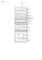
第3の実施形態は、フリー層及び2つのピン層のそれぞれに面内磁化膜を用いて、MTJ素子10を構成するようにしている。図10は、本発明の第3の実施形態に係るMTJ素子10の構成を示す斜視図である。図10は、本実施形態のMTJ素子10の基本構成を示している。
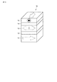
(Third embodiment)
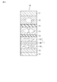
In the third embodiment, the
MTJ素子10は、第1のピン層11、第1の中間層12、フリー層13、第2の中間層14、第2のピン層15が順に積層された積層構造を有している。なお、この基本構成は、積層順序が逆転していても構わない。
The
ピン層11、フリー層13、ピン層15の容易磁化方向は、膜面に対して平行である。すなわち、全ての磁性層として面内磁化膜を用いることが可能となり、MTJ素子10を容易に形成することができる。
The easy magnetization directions of the pinned
また、ピン層11とフリー層13とは容易磁化方向が平行であり、ピン層11とピン層15とは容易磁化方向が互いに直交している。従って、磁化配列が平行となるフリー層13とピン層11との間では中間層12を介して磁気抵抗効果が発現するが、磁化配列が垂直となるフリー層13とピン層15との間では中間層14を介した磁気抵抗効果は発現しない。
The pinned
図11は、MTJ素子10の具体例を示す斜視図である。図10に示した基本構成の最上層及び最下層にそれぞれ、キャップ層17及び下地層16が設けられている。ピン層11は、ピン層11C/中間層11B/ピン層11Aの積層構造を有している。すなわち、ピン層11は、SAF構造を有している。ピン層11A及びピン層11Cの容易磁化方向は、膜面に対して平行である。また、ピン層11Aとピン層11Cとの磁化の方向は互いに反平行に設定され、ピン層11Aとピン層11Cとは中間層11Bを挟んで反強磁性結合している。
FIG. 11 is a perspective view showing a specific example of the
さらに、ピン層11Aの下(ピン層11Aと下地層16との間)には、ピン層11Aと接するように、反強磁性層19が設けられている。ピン層11Aは、反強磁性層19と交換結合することで、膜面に対して平行に磁化の方向が固着されている。この構造を用いることで、ピン層11Aの磁化固着力が増強され、外部磁場に対する耐性及び熱的な安定性が向上する。
Further, an
また、ピン層15は、フリー層13と明確な保持力差を設ける必要がある。このため、ピン層15としては、面内磁化型硬質磁性層を用いることが好ましい。
Further, the pinned
面内磁化型硬質磁性層の材料としては、Co−Pt合金、或いはCo−Pt−X合金(Xは、Cr、Ta、Pd、B、Si、Ruから選ばれる少なくとも1つ以上の元素)があげられる。また、面内磁化型硬質磁性層を用いた硬質磁性層/中間層/硬質磁性層の構成を有するSAF構造も形成可能である。この場合、中間層にはRu或いはOsが用いられる。 As a material of the in-plane magnetization type hard magnetic layer, a Co—Pt alloy or a Co—Pt—X alloy (X is at least one element selected from Cr, Ta, Pd, B, Si, Ru). can give. Further, a SAF structure having a configuration of hard magnetic layer / intermediate layer / hard magnetic layer using an in-plane magnetization type hard magnetic layer can be formed. In this case, Ru or Os is used for the intermediate layer.
図12は、ピン層15の他の構成を示す斜視図である。ピン層15上(ピン層15とキャップ層17との間)には、ピン層15と接するように、反強磁性層18が設けられている。ピン層15は、反強磁性層18と交換結合することで、膜面に対して平行に磁化の方向が固着されている。
FIG. 12 is a perspective view showing another configuration of the pinned
図13は、ピン層15の他の構成を示す斜視図である。ピン層15は、ピン層15C/中間層15B/ピン層15Aの積層構造を有している。すなわち、ピン層15は、SAF構造を有している。ピン層15A及びピン層15Cの容易磁化方向は、膜面に対して平行である。また、ピン層15Aとピン層15Cとの磁化の方向は互いに反平行に設定され、ピン層15Aとピン層15Cとは中間層15Bを挟んで反強磁性結合している。
FIG. 13 is a perspective view showing another configuration of the pinned
図12および図13に示した反強磁性層19及び反強磁性層18は、強磁性層との結合の臨界温度すなわちブロッキング温度に差をつけることで、アニールシーケンスによりピン層11とピン層15との容易磁化方向を直交化することが可能となる。より具体的には、反強磁性層19にはPtMnやNiMnなどの高いブロッキング温度を有する材料を用い、反強磁性層18にはFeMnやIrMnなどの比較的低いブロッキング温度を有するものを用いることが好ましい。
The
また、フリー層13は、強磁性層/中間層/強磁性層の積層構造、すなわち、SAF構造を有していても構わない。SAF構造において、強磁性層同士の磁化の方向は互いに反平行に設定され、中間層を挟んで反強磁性結合している。
The
このようにしてMTJ素子10を構成した場合でも、上記第1の実施形態と同様の効果を得ることができる。なお、上記第1の実施形態で示したように、フリー層13及びピン層11に界面層を挿入してもよい。また、MTJ素子10を構成する各層の材料については、上記第1及び第2の実施形態で示した材料を用いることができる。
Even when the
(第4の実施形態)
第4の実施形態は、前述したMTJ素子10を用いてMRAMを構成した場合の実施例について示している。
(Fourth embodiment)
The fourth embodiment shows an example in which an MRAM is configured using the
図14は、本発明の第4の実施形態に係るMRAMの構成を示す回路図である。MRAMは、マトリクス状に配列された複数のメモリセルMCを有するメモリセルアレイ20を備えている。メモリセルアレイ20には、それぞれが列(カラム)方向に延在するように、複数のビット線BLが配置されている。また、メモリセルアレイ20には、それぞれが行(ロウ)方向に延在するように、複数のワード線WLが配置されている。
FIG. 14 is a circuit diagram showing a configuration of an MRAM according to the fourth embodiment of the present invention. The MRAM includes a
ビット線BLとワード線WLとの交差部分には、前述したメモリセルMCが配置されている。各メモリセルMCは、MTJ素子10と選択トランジスタ21とにより構成されている。MTJ素子10の一端は、ビット線BLに接続されている。MTJ素子10の他端は、選択トランジスタ21のドレインに接続されている。選択トランジスタ21のゲートには、ワード線WLが接続されている。選択トランジスタ21のソースは、ソース線SLに接続されている。
The memory cell MC described above is arranged at the intersection between the bit line BL and the word line WL. Each memory cell MC includes an
ビット線BLの一端には、電源回路22が接続されている。ビット線BLの他端には、センスアンプ回路24が接続されている。ソース線SLの一端には、電源回路23が接続されている。ソース線SLの他端は、図示しないスイッチ素子を介して電源25に接続されている。
A power supply circuit 22 is connected to one end of the bit line BL. A
電源回路22は、ビット線BLの一端に正の電位を印加する。センスアンプ回路24は、MTJ素子10の抵抗値を検出する他、ビット線BLの他端に例えば接地電位を印加する。電源回路23は、ソース線SLの一端に、正の電位を印加する。電源25は、この電源25に接続されたスイッチ素子をオンすることにより、ソース線SLの他端に例えば接地電位を印加する。また、各電源回路は、対応する配線との電気的な接続を制御するスイッチ素子を含んでいる。
The power supply circuit 22 applies a positive potential to one end of the bit line BL. The
メモリセルMCへのデータ書き込みは、以下のように行われる。先ず、データ書き込みを行うメモリセルMCを選択するために、このメモリセルMCに接続されたワード線WLが活性化される。これにより、選択トランジスタ21がターンオンする。
Data writing to the memory cell MC is performed as follows. First, in order to select a memory cell MC for writing data, the word line WL connected to the memory cell MC is activated. As a result, the
ここで、MTJ素子10には、双方向の書き込み電流Iwが供給される。具体的には、MTJ素子10に上から下へ書き込み電流Iwを供給する場合、電源回路22はビット線BLの一端に正の電位を印加し、電源25はこの電源25に対応するスイッチ素子をオンすることによりソース線SLの他端に接地電位を印加する。
Here, the bidirectional write current Iw is supplied to the
また、MTJ素子10に下から上へ書き込み電流Iwを供給する場合、電源回路23はソース線SLの一端に正の電位を印加し、センスアンプ回路24はビット線BLの他端に接地電位を印加する。ここでは、電源25に対応するスイッチ素子はオフされている。このようして、メモリセルMCにデータ“0”或いはデータ“1”を書き込むことができる。
When supplying the write current Iw from the bottom to the top to the
メモリセルMCからのデータ読み出しは、以下のように行われる。先ず、メモリセルMCが選択される。次に、電源回路23及びセンスアンプ回路24により、MTJ素子10には、電源回路23からセンスアンプ回路24へ流れる読み出し電流Irが供給される。そして、センスアンプ回路24は、この読み出し電流Irに基づいて、MTJ素子10の抵抗値を検出する。このようにして、MTJ素子10に記憶された情報を読み出すことができる。
Data reading from the memory cell MC is performed as follows. First, the memory cell MC is selected. Next, the read current Ir flowing from the power supply circuit 23 to the
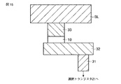
次に、MRAMの構造について説明する。図15は、MTJ素子10を中心に示したMRAMの断面図である。MTJ素子10は、シリコンなどからなる半導体基板(図示せず)に形成された選択トランジスタ21の上方に層間絶縁層を介して形成される。
Next, the structure of the MRAM will be described. FIG. 15 is a cross-sectional view of the MRAM centered on the
引き出し電極32上には、MTJ素子10が設けられている。引き出し電極32は、ビアプラグ31を介して選択トランジスタ21のドレイン領域に電気的に接続される。MTJ素子10上には、導電性のハードマスク33が設けられている。ハードマスク33上には、ビット線BLが設けられている。
An
ビット線BL、ハードマスク33及びビアプラグ31としては、W、Al、Cu及びAlCuなどが用いられる。Cuを用いた金属配線層或いはビアプラグの場合には、Cuダマシン或いはCuデュアルダマシンプロセスが用いられる。
As the bit line BL, the
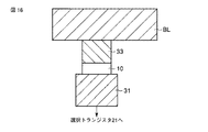
図16は、MTJ素子10を中心に示したMRAMの他の構成例である。ビアプラグ31上には、直接にMTJ素子10が設けられている。すなわち、図16のMRAMは、図15のMRAMと比べて、引き出し電極32が省略されている。MTJ素子10上には、ハードマスク33が設けられている。ハードマスク33上には、ビット線BLが設けられている。
FIG. 16 shows another configuration example of the MRAM centered on the
MTJ素子10は、図15に示されるように引き出し電極32によりビアプラグ31と電気的に接続される場合と、図16に示されるようにMTJ素子10がビアプラグ31上に直接形成される場合とがある。図16の構成を用いる場合、ビアサイズよりもMTJ素子サイズが小さい方が好ましい。
The
リソグラフィやエッチング技術等によって決まる最小加工寸法をF(Minimum Feature Size)とすると、図15のレイアウトを用いた場合、最小セルサイズは8F2である。これに対して、図16のレイアウトを用いた場合、最小セルサイズが4F2にまで縮小することが可能となる。 Assuming that the minimum processing dimension determined by lithography, etching technology, etc. is F (Minimum Feature Size), the minimum cell size is 8F 2 when the layout of FIG. 15 is used. On the other hand, when the layout of FIG. 16 is used, the minimum cell size can be reduced to 4F 2 .
このように構成されたMRAMにおいて、MTJ素子10に情報を書き込む際の書き込み速度を向上させることができる。具体的には、書き込み速度としては、数ナノ秒から数マイクロ秒までのパルス幅を有する電流でスピン注入書き込みを行うことが可能となる。
In the MRAM configured as described above, the writing speed when writing information to the
なお、読み出し時にMTJ素子10に供給される読み出し電流Irは、書き込み時にMTJ素子10に供給される書き込み電流Iwよりもパルス幅が短いことが望ましい。これにより、読み出し電流Irでの誤書き込みを低減することができる。これは、書き込み電流Iwのパルス幅が短い方が、書き込み電流値の絶対値が大きくなるということに基づいている。
The read current Ir supplied to the
本発明は、上述した実施形態に限定されるものではなく、その要旨を逸脱しない範囲内で、構成要素を変形して具体化できる。また、実施形態に開示されている複数の構成要素の適宜な組み合わせにより種々の発明を構成することができる。例えば、実施形態に開示される全構成要素から幾つかの構成要素を削除してもよいし、異なる実施形態の構成要素を適宜組み合わせてもよい。 The present invention is not limited to the above-described embodiment, and can be embodied by modifying the constituent elements without departing from the scope of the invention. In addition, various inventions can be configured by appropriately combining a plurality of constituent elements disclosed in the embodiments. For example, some constituent elements may be deleted from all the constituent elements disclosed in the embodiments, or constituent elements of different embodiments may be appropriately combined.
10…MTJ素子、11…第1の磁化参照層(ピン層)、11A,11C,11D…ピン層、11B…中間層、11E…界面ピン層、12…第1の中間層、13…磁化自由層(フリー層)、13A,13C…界面フリー層、13B,13F,13D…フリー層、13E…中間層、14…第2の中間層、15…第2の磁化参照層(ピン層)、15A,15C…ピン層、15B…中間層、16…下地層、17…キャップ層、18,19…反強磁性層、20…メモリセルアレイ、21…選択トランジスタ、22,23…電源回路、24…センスアンプ回路、25…電源、31…ビアプラグ、32…引き出し電極、33…ハードマスク、MC…メモリセル、BL…ビット線、WL…ワード線、SL…ソース線。
DESCRIPTION OF
Claims (14)
スピン偏極した電子の作用により磁化の方向が変化する磁化自由層と、
磁化の方向が固定された第2の磁化参照層と、
前記第1の磁化参照層と前記磁化自由層との間に設けられた第1の中間層と、
前記磁化自由層と前記第2の磁化参照層との間に設けられた第2の中間層と、
を具備し、
前記磁化自由層及び前記第1の磁化参照層の容易磁化方向は、膜面に対して垂直或いは平行であり、
前記第1の磁化参照層と前記第2の磁化参照層との容易磁化方向は、互いに直交することを特徴とする磁気抵抗素子。 A first magnetization reference layer having a fixed magnetization direction;
A magnetization free layer in which the direction of magnetization changes due to the action of spin-polarized electrons,
A second magnetization reference layer having a fixed magnetization direction;
A first intermediate layer provided between the first magnetization reference layer and the magnetization free layer;
A second intermediate layer provided between the magnetization free layer and the second magnetization reference layer;
Comprising
The easy magnetization directions of the magnetization free layer and the first magnetization reference layer are perpendicular or parallel to the film surface,
2. The magnetoresistive element according to claim 1, wherein easy magnetization directions of the first magnetization reference layer and the second magnetization reference layer are orthogonal to each other.
前記第2の磁化参照層の容易磁化方向は、膜面に対して平行であることを特徴とする請求項1に記載の磁気抵抗素子。 The easy magnetization directions of the magnetization free layer and the first magnetization reference layer are perpendicular to the film surface,
The magnetoresistive element according to claim 1, wherein the easy magnetization direction of the second magnetization reference layer is parallel to the film surface.
前記第1の界面磁性層は、前記第1の中間層に接するように配置され、
前記第2の界面磁性層は、前記第2の中間層に接するように配置されることを特徴とする請求項1乃至4のいずれかに記載の磁気抵抗素子。 The magnetization free layer includes a first interface magnetic layer, a main magnetic layer, and a second interface magnetic layer, which are sequentially stacked,
The first interfacial magnetic layer is disposed so as to contact the first intermediate layer,
5. The magnetoresistive element according to claim 1, wherein the second interface magnetic layer is disposed in contact with the second intermediate layer. 6.
前記第3の界面磁性層は、前記第1の中間層に接するように配置されることを特徴とする請求項1乃至5のいずれかに記載の磁気抵抗素子。 The first magnetization reference layer includes a laminated main magnetic layer and a third interface magnetic layer,
6. The magnetoresistive element according to claim 1, wherein the third interface magnetic layer is disposed so as to be in contact with the first intermediate layer.
Priority Applications (1)
| Application Number | Priority Date | Filing Date | Title |
|---|---|---|---|
| JP2007044176A JP2008028362A (en) | 2006-06-22 | 2007-02-23 | Magnetoresistive element and magnetic memory |
Applications Claiming Priority (2)
| Application Number | Priority Date | Filing Date | Title |
|---|---|---|---|
| JP2006172844 | 2006-06-22 | ||
| JP2007044176A JP2008028362A (en) | 2006-06-22 | 2007-02-23 | Magnetoresistive element and magnetic memory |
Publications (1)
| Publication Number | Publication Date |
|---|---|
| JP2008028362A true JP2008028362A (en) | 2008-02-07 |
Family
ID=39118644
Family Applications (1)
| Application Number | Title | Priority Date | Filing Date |
|---|---|---|---|
| JP2007044176A Abandoned JP2008028362A (en) | 2006-06-22 | 2007-02-23 | Magnetoresistive element and magnetic memory |
Country Status (1)
| Country | Link |
|---|---|
| JP (1) | JP2008028362A (en) |
Cited By (49)
| Publication number | Priority date | Publication date | Assignee | Title |
|---|---|---|---|---|
| JP2009212156A (en) * | 2008-02-29 | 2009-09-17 | Toshiba Corp | Magnetoresistive element and magnetic memory using the same |
| WO2009122995A1 (en) * | 2008-04-03 | 2009-10-08 | 日本電気株式会社 | Magnetoresistive storage device |
| JP2009231753A (en) * | 2008-03-25 | 2009-10-08 | Toshiba Corp | Magnetoresistance effect element and magnetic random access memory |
| WO2009122992A1 (en) * | 2008-04-03 | 2009-10-08 | 日本電気株式会社 | Magnetoresistance storage |
| JP2009239121A (en) * | 2008-03-27 | 2009-10-15 | Toshiba Corp | Magnetoresistive element and magnetic random access memory |
| WO2009145161A1 (en) * | 2008-05-28 | 2009-12-03 | 株式会社日立製作所 | Magnetic memory cell and magnetic random access memory |
| JP2010073960A (en) * | 2008-09-19 | 2010-04-02 | Toshiba Corp | Semiconductor device |
| JP2010219412A (en) * | 2009-03-18 | 2010-09-30 | Toshiba Corp | Magnetoresistive element and magnetic random access memory |
| JP2010238288A (en) * | 2009-03-30 | 2010-10-21 | Toshiba Corp | Magnetoresistive memory |
| WO2010134378A1 (en) | 2009-05-19 | 2010-11-25 | 富士電機ホールディングス株式会社 | Magnetic memory element and storage device using same |
| WO2011001746A1 (en) | 2009-07-03 | 2011-01-06 | 富士電機ホールディングス株式会社 | Magnetic memory element and driving method therefor |
| JP2011023722A (en) * | 2009-07-14 | 2011-02-03 | Crocus Technology Sa | Magnetic element with fast spin transfer torque writing procedure |
| WO2011093252A1 (en) * | 2010-01-26 | 2011-08-04 | 株式会社日立製作所 | Magnetoresistive effect element, magnetic memory cell using same, and random access memory |
| WO2011096312A1 (en) * | 2010-02-04 | 2011-08-11 | 株式会社日立製作所 | Tunnel magnetoresistance effect element, and magnetic memory cell and magnetic random access memory employing same |
| JP2012004222A (en) * | 2010-06-15 | 2012-01-05 | Sony Corp | Memory |
| WO2012036282A1 (en) * | 2010-09-17 | 2012-03-22 | 株式会社 東芝 | Magnetoresistive element and magnetic random-access memory |
| JP2012510731A (en) * | 2008-12-03 | 2012-05-10 | シーゲイト テクノロジー エルエルシー | Magnetic random access memory with double spin torque reference layer |
| JP2012146984A (en) * | 2011-01-13 | 2012-08-02 | Crocus Technology Sa | Magnetic tunnel junction comprising polarizing layer |
| JP2012178541A (en) * | 2010-11-26 | 2012-09-13 | Renesas Electronics Corp | Magnetic memory |
| JP2012525710A (en) * | 2009-04-28 | 2012-10-22 | シーゲイト テクノロジー エルエルシー | Magnetic layered body having spin torque switching and having a layer for assisting switching of spin torque |
| JP2012533190A (en) * | 2009-07-13 | 2012-12-20 | シーゲイト テクノロジー エルエルシー | Resistive sensing element assisted by static magnetic field |
| JP2012533189A (en) * | 2009-07-13 | 2012-12-20 | シーゲイト テクノロジー エルエルシー | Magnetic stack with reference layer with orthogonal magnetization orientation direction |
| US8405173B2 (en) | 2010-06-15 | 2013-03-26 | Samsung Electronics Co., Ltd. | Magnetic memory devices |
| JP2013069788A (en) * | 2011-09-21 | 2013-04-18 | Toshiba Corp | Magnetoresistance effect element, magnetic memory and method for manufacturing magnetoresistance effect element |
| JP2013522931A (en) * | 2010-03-26 | 2013-06-13 | クアルコム,インコーポレイテッド | Damascene magnetic tunnel junction structure having horizontal and vertical portions and method for manufacturing the same |
| US8467149B2 (en) | 2010-11-26 | 2013-06-18 | Kabushiki Kaisha Toshiba | Spin torque oscillator and magnetic recording apparatus |
| JP2013531358A (en) * | 2010-03-17 | 2013-08-01 | グランディス インコーポレイテッド | Method and system for providing an inverted dual magnetic tunnel junction element |
| US8537506B2 (en) | 2009-10-14 | 2013-09-17 | Samsung Electronics Co., Ltd. | Information storage device with domain wall moving unit and magneto-resistive device magnetization arrangement |
| JP2013191873A (en) * | 2013-05-21 | 2013-09-26 | Nec Corp | Magnetic random access memory |
| JP2013197344A (en) * | 2012-03-21 | 2013-09-30 | Toshiba Corp | Magnetoresistance effect element and magnetic memory |
| JP2013251042A (en) * | 2013-07-19 | 2013-12-12 | Toshiba Corp | Spin torque oscillator, magnetic recording head, magnetic head assembly, and magnetic recorder |
| JP2013254957A (en) * | 2012-06-07 | 2013-12-19 | Samsung Electronics Co Ltd | Magnetic tunneling junction seed film, capping film, and spacer film material |
| JP2014003313A (en) * | 2013-08-06 | 2014-01-09 | Canon Anelva Corp | Manufacturing process of tunnel magnetoresistive element |
| KR20140009071A (en) * | 2012-07-13 | 2014-01-22 | 삼성전자주식회사 | Method and system for providing magnetic tunneling junctions usable in spin transfer torque magnetic memories |
| JP2014064033A (en) * | 2009-06-24 | 2014-04-10 | New York Univ | High speed low power magnetic device based on current-induced spin-momentum transfer |
| JP5527669B2 (en) * | 2009-05-22 | 2014-06-18 | 独立行政法人物質・材料研究機構 | Ferromagnetic tunnel junction and magnetoresistive effect element using the same |
| US8995179B2 (en) | 2009-09-17 | 2015-03-31 | Fuji Electric Co., Ltd. | Magnetoresistance element and non-volatile semiconductor storage device using same magnetoresistance element |
| JP2015088520A (en) * | 2013-10-28 | 2015-05-07 | ソニー株式会社 | Storage element, storage device and magnetic head |
| JP2015525426A (en) * | 2012-05-31 | 2015-09-03 | ノースロップ グラマン システムズ コーポレイションNorthrop Grumman Systems Corporation | Josephson magnetic memory cell system |
| JP2015534272A (en) * | 2012-09-21 | 2015-11-26 | コリア ユニバーシティ リサーチ アンド ビジネス ファウンデーション | Magnetic memory device using in-plane current and electric field |
| WO2017010549A1 (en) * | 2015-07-16 | 2017-01-19 | 国立大学法人東北大学 | Magnetoresistive element and magnetic memory |
| JP2017510989A (en) * | 2014-04-01 | 2017-04-13 | スピン トランスファー テクノロジーズ インク | Magnetic tunnel junction structure for MRAM device |
| WO2017086481A1 (en) * | 2015-11-18 | 2017-05-26 | 国立大学法人東北大学 | Magnetic tunnel junction element and magnetic memory |
| JP2017133886A (en) * | 2016-01-26 | 2017-08-03 | 株式会社東芝 | Magnetic sensor and magnetic sensor device |
| JP2017212464A (en) * | 2017-08-09 | 2017-11-30 | ソニー株式会社 | Storage element, storage device, and magnetic head |
| KR20180018779A (en) * | 2015-06-16 | 2018-02-21 | 스핀 트랜스퍼 테크놀로지스, 인크. | Spin current structure for MRAM |
| CN111725388A (en) * | 2019-03-18 | 2020-09-29 | 东芝存储器株式会社 | Magnetic device |
| WO2020246553A1 (en) * | 2019-06-06 | 2020-12-10 | 国立大学法人東北大学 | Magnetoresistance effect element and magnetic storage device |
| CN114764007A (en) * | 2021-01-11 | 2022-07-19 | 大银微系统股份有限公司 | Position sensing mechanism |
-
2007
- 2007-02-23 JP JP2007044176A patent/JP2008028362A/en not_active Abandoned
Cited By (77)
| Publication number | Priority date | Publication date | Assignee | Title |
|---|---|---|---|---|
| JP2009212156A (en) * | 2008-02-29 | 2009-09-17 | Toshiba Corp | Magnetoresistive element and magnetic memory using the same |
| US8279663B2 (en) | 2008-03-25 | 2012-10-02 | Kabushiki Kaisha Toshiba | Magnetoresistance effect element and magnetic random access memory |
| JP2009231753A (en) * | 2008-03-25 | 2009-10-08 | Toshiba Corp | Magnetoresistance effect element and magnetic random access memory |
| US8014193B2 (en) | 2008-03-25 | 2011-09-06 | Kabushiki Kaisha Toshiba | Magnetoresistance effect element and magnetic random access memory |
| JP2009239121A (en) * | 2008-03-27 | 2009-10-15 | Toshiba Corp | Magnetoresistive element and magnetic random access memory |
| WO2009122995A1 (en) * | 2008-04-03 | 2009-10-08 | 日本電気株式会社 | Magnetoresistive storage device |
| WO2009122992A1 (en) * | 2008-04-03 | 2009-10-08 | 日本電気株式会社 | Magnetoresistance storage |
| JP5356377B2 (en) * | 2008-05-28 | 2013-12-04 | 株式会社日立製作所 | Magnetic memory cell and magnetic random access memory |
| US8508985B2 (en) | 2008-05-28 | 2013-08-13 | Hitachi, Ltd. | Magnetic memory cell and magnetic random access memory |
| WO2009145161A1 (en) * | 2008-05-28 | 2009-12-03 | 株式会社日立製作所 | Magnetic memory cell and magnetic random access memory |
| JP2010073960A (en) * | 2008-09-19 | 2010-04-02 | Toshiba Corp | Semiconductor device |
| JP2012510731A (en) * | 2008-12-03 | 2012-05-10 | シーゲイト テクノロジー エルエルシー | Magnetic random access memory with double spin torque reference layer |
| JP2010219412A (en) * | 2009-03-18 | 2010-09-30 | Toshiba Corp | Magnetoresistive element and magnetic random access memory |
| JP2010238288A (en) * | 2009-03-30 | 2010-10-21 | Toshiba Corp | Magnetoresistive memory |
| US8472242B2 (en) | 2009-03-30 | 2013-06-25 | Kabushiki Kaisha Toshiba | Magnetoresistive effect memory |
| JP2012525710A (en) * | 2009-04-28 | 2012-10-22 | シーゲイト テクノロジー エルエルシー | Magnetic layered body having spin torque switching and having a layer for assisting switching of spin torque |
| US8514617B2 (en) | 2009-05-19 | 2013-08-20 | Fuji Electric Co., Ltd. | Magnetic memory element and storage device using the same |
| KR20120027122A (en) | 2009-05-19 | 2012-03-21 | 후지 덴키 가부시키가이샤 | Magnetic memory element and storage device using same |
| WO2010134378A1 (en) | 2009-05-19 | 2010-11-25 | 富士電機ホールディングス株式会社 | Magnetic memory element and storage device using same |
| JP5527669B2 (en) * | 2009-05-22 | 2014-06-18 | 独立行政法人物質・材料研究機構 | Ferromagnetic tunnel junction and magnetoresistive effect element using the same |
| JP2014064033A (en) * | 2009-06-24 | 2014-04-10 | New York Univ | High speed low power magnetic device based on current-induced spin-momentum transfer |
| US8750028B2 (en) | 2009-07-03 | 2014-06-10 | Fuji Electric Co., Ltd. | Magnetic memory element and driving method for same |
| JP5321991B2 (en) * | 2009-07-03 | 2013-10-23 | 富士電機株式会社 | Magnetic memory device and driving method thereof |
| WO2011001746A1 (en) | 2009-07-03 | 2011-01-06 | 富士電機ホールディングス株式会社 | Magnetic memory element and driving method therefor |
| JP2013153194A (en) * | 2009-07-13 | 2013-08-08 | Seagate Technology Llc | Static magnetic field assisted resistive sense element |
| JP2012533190A (en) * | 2009-07-13 | 2012-12-20 | シーゲイト テクノロジー エルエルシー | Resistive sensing element assisted by static magnetic field |
| JP2012533189A (en) * | 2009-07-13 | 2012-12-20 | シーゲイト テクノロジー エルエルシー | Magnetic stack with reference layer with orthogonal magnetization orientation direction |
| JP2011023722A (en) * | 2009-07-14 | 2011-02-03 | Crocus Technology Sa | Magnetic element with fast spin transfer torque writing procedure |
| EP3703113A2 (en) | 2009-09-17 | 2020-09-02 | III Holdings 3, LLC | Magnetoresistance element and non-volatile semiconductor storage device using same magnetoresistance element |
| US8995179B2 (en) | 2009-09-17 | 2015-03-31 | Fuji Electric Co., Ltd. | Magnetoresistance element and non-volatile semiconductor storage device using same magnetoresistance element |
| US10468591B2 (en) | 2009-09-17 | 2019-11-05 | Iii Holdings 3, Llc | Magnetoresistance element and non-volatile semiconductor storage device using same magnetoresistance element |
| US10756261B2 (en) | 2009-09-17 | 2020-08-25 | Iii Holdings 3, Ltd. | Magnetoresistance element and non-volatile semiconductor storage device using same magnetoresistance element |
| US9525127B2 (en) | 2009-09-17 | 2016-12-20 | Iii Holdings 3, Llc | Magnetoresistance element and non-volatile semiconductor storage device using same magnetoresistance element |
| US8537506B2 (en) | 2009-10-14 | 2013-09-17 | Samsung Electronics Co., Ltd. | Information storage device with domain wall moving unit and magneto-resistive device magnetization arrangement |
| US9042165B2 (en) | 2010-01-26 | 2015-05-26 | Hitachi, Ltd. | Magnetoresistive effect element, magnetic memory cell using same, and random access memory |
| WO2011093252A1 (en) * | 2010-01-26 | 2011-08-04 | 株式会社日立製作所 | Magnetoresistive effect element, magnetic memory cell using same, and random access memory |
| WO2011096312A1 (en) * | 2010-02-04 | 2011-08-11 | 株式会社日立製作所 | Tunnel magnetoresistance effect element, and magnetic memory cell and magnetic random access memory employing same |
| JP2013531358A (en) * | 2010-03-17 | 2013-08-01 | グランディス インコーポレイテッド | Method and system for providing an inverted dual magnetic tunnel junction element |
| US9385308B2 (en) | 2010-03-26 | 2016-07-05 | Qualcomm Incorporated | Perpendicular magnetic tunnel junction structure |
| JP2015156488A (en) * | 2010-03-26 | 2015-08-27 | クアルコム,インコーポレイテッド | Damascene type magnetic tunnel junction structure with horizontal and perpendicular portions, and method of fabricating the same |
| JP2013522931A (en) * | 2010-03-26 | 2013-06-13 | クアルコム,インコーポレイテッド | Damascene magnetic tunnel junction structure having horizontal and vertical portions and method for manufacturing the same |
| US8405173B2 (en) | 2010-06-15 | 2013-03-26 | Samsung Electronics Co., Ltd. | Magnetic memory devices |
| JP2012004222A (en) * | 2010-06-15 | 2012-01-05 | Sony Corp | Memory |
| WO2012036282A1 (en) * | 2010-09-17 | 2012-03-22 | 株式会社 東芝 | Magnetoresistive element and magnetic random-access memory |
| JP2012178541A (en) * | 2010-11-26 | 2012-09-13 | Renesas Electronics Corp | Magnetic memory |
| US8467149B2 (en) | 2010-11-26 | 2013-06-18 | Kabushiki Kaisha Toshiba | Spin torque oscillator and magnetic recording apparatus |
| JP2012146984A (en) * | 2011-01-13 | 2012-08-02 | Crocus Technology Sa | Magnetic tunnel junction comprising polarizing layer |
| JP2013069788A (en) * | 2011-09-21 | 2013-04-18 | Toshiba Corp | Magnetoresistance effect element, magnetic memory and method for manufacturing magnetoresistance effect element |
| US8937832B2 (en) | 2012-03-21 | 2015-01-20 | Kabushiki Kaisha Toshiba | Magnetic memory |
| JP2013197344A (en) * | 2012-03-21 | 2013-09-30 | Toshiba Corp | Magnetoresistance effect element and magnetic memory |
| JP2015525426A (en) * | 2012-05-31 | 2015-09-03 | ノースロップ グラマン システムズ コーポレイションNorthrop Grumman Systems Corporation | Josephson magnetic memory cell system |
| JP2013254957A (en) * | 2012-06-07 | 2013-12-19 | Samsung Electronics Co Ltd | Magnetic tunneling junction seed film, capping film, and spacer film material |
| KR20140009071A (en) * | 2012-07-13 | 2014-01-22 | 삼성전자주식회사 | Method and system for providing magnetic tunneling junctions usable in spin transfer torque magnetic memories |
| KR102042769B1 (en) * | 2012-07-13 | 2019-11-08 | 삼성전자주식회사 | Method and system for providing magnetic tunneling junctions usable in spin transfer torque magnetic memories |
| JP2014022735A (en) * | 2012-07-13 | 2014-02-03 | Samsung Electronics Co Ltd | Method and system for providing magnetic tunneling junctions usable in spin transfer torque magnetic memories |
| JP2015534272A (en) * | 2012-09-21 | 2015-11-26 | コリア ユニバーシティ リサーチ アンド ビジネス ファウンデーション | Magnetic memory device using in-plane current and electric field |
| JP2013191873A (en) * | 2013-05-21 | 2013-09-26 | Nec Corp | Magnetic random access memory |
| JP2013251042A (en) * | 2013-07-19 | 2013-12-12 | Toshiba Corp | Spin torque oscillator, magnetic recording head, magnetic head assembly, and magnetic recorder |
| JP2014003313A (en) * | 2013-08-06 | 2014-01-09 | Canon Anelva Corp | Manufacturing process of tunnel magnetoresistive element |
| JP2015088520A (en) * | 2013-10-28 | 2015-05-07 | ソニー株式会社 | Storage element, storage device and magnetic head |
| JP2017510989A (en) * | 2014-04-01 | 2017-04-13 | スピン トランスファー テクノロジーズ インク | Magnetic tunnel junction structure for MRAM device |
| KR20180018779A (en) * | 2015-06-16 | 2018-02-21 | 스핀 트랜스퍼 테크놀로지스, 인크. | Spin current structure for MRAM |
| KR102479222B1 (en) * | 2015-06-16 | 2022-12-19 | 인테그레이티드 실리콘 솔루션, (케이만) 인코포레이티드 | Precession Spin Current Structure for MRAM |
| JP2018522409A (en) * | 2015-06-16 | 2018-08-09 | スピン トランスファー テクノロジーズ インク | Precession spin current structure for MRAM |
| US10658572B2 (en) | 2015-07-16 | 2020-05-19 | Tohoku University | Magnetoresistance effect element and magnetic memory |
| US10164174B2 (en) | 2015-07-16 | 2018-12-25 | Tohoku University | Magnetoresistance effect element and magnetic memory |
| WO2017010549A1 (en) * | 2015-07-16 | 2017-01-19 | 国立大学法人東北大学 | Magnetoresistive element and magnetic memory |
| JPWO2017010549A1 (en) * | 2015-07-16 | 2018-05-31 | 国立大学法人東北大学 | Magnetoresistive element and magnetic memory |
| WO2017086481A1 (en) * | 2015-11-18 | 2017-05-26 | 国立大学法人東北大学 | Magnetic tunnel junction element and magnetic memory |
| JPWO2017086481A1 (en) * | 2015-11-18 | 2018-09-20 | 国立大学法人東北大学 | Magnetic tunnel junction device and magnetic memory |
| US11563169B2 (en) | 2015-11-18 | 2023-01-24 | Tohoku University | Magnetic tunnel junction element and magnetic memory |
| JP2017133886A (en) * | 2016-01-26 | 2017-08-03 | 株式会社東芝 | Magnetic sensor and magnetic sensor device |
| JP2017212464A (en) * | 2017-08-09 | 2017-11-30 | ソニー株式会社 | Storage element, storage device, and magnetic head |
| CN111725388A (en) * | 2019-03-18 | 2020-09-29 | 东芝存储器株式会社 | Magnetic device |
| WO2020246553A1 (en) * | 2019-06-06 | 2020-12-10 | 国立大学法人東北大学 | Magnetoresistance effect element and magnetic storage device |
| CN114764007A (en) * | 2021-01-11 | 2022-07-19 | 大银微系统股份有限公司 | Position sensing mechanism |
| CN114764007B (en) * | 2021-01-11 | 2024-05-07 | 大银微系统股份有限公司 | Position sensing mechanism |
Similar Documents
| Publication | Publication Date | Title |
|---|---|---|
| KR100832191B1 (en) | Magnetoresistive element and magnetic memory | |
| JP2008028362A (en) | Magnetoresistive element and magnetic memory | |
| US9978933B2 (en) | Storage element and memory | |
| JP2008010590A (en) | Magnetoresistive element, and magnetic memory | |
| US7924607B2 (en) | Magnetoresistance effect element and magnetoresistive random access memory using the same | |
| JP2008252037A (en) | Magnetoresistive element, and magnetic memory | |
| EP1933338B1 (en) | Magnetic storage element and memory | |
| US9147455B2 (en) | Storage element having laminated storage layer including magnetic layer and conductive oxide and storage device including the storage element | |
| JP2007150265A (en) | Magnetoresistive element and magnetic storage | |
| JP4970113B2 (en) | Magnetoresistive element and magnetic memory | |
| US8565013B2 (en) | Storage element and storage device | |
| US20070096229A1 (en) | Magnetoresistive element and magnetic memory device | |
| JP2009094104A (en) | Magnetoresistive element | |
| JP6244617B2 (en) | Storage element, storage device, magnetic head | |
| JP4277870B2 (en) | Storage element and memory | |
| US8692341B2 (en) | Storage element and storage device | |
| JP2008109118A (en) | Magnetoresistance effect element and magnetic random access memory using it | |
| KR101891829B1 (en) | Memory element and memory device | |
| US10170694B1 (en) | Magnetic memory | |
| WO2011036795A1 (en) | Magnetoresistive effect element and magnetic memory | |
| WO2016080273A1 (en) | Magnetoresistive element and magnetic memory | |
| US9991314B2 (en) | Magnetoresistive element and magnetic memory | |
| JP2006295001A (en) | Storage element and memory | |
| JP2017212464A (en) | Storage element, storage device, and magnetic head |
Legal Events
| Date | Code | Title | Description |
|---|---|---|---|
| A762 | Written abandonment of application |
Free format text: JAPANESE INTERMEDIATE CODE: A762 Effective date: 20100108 |