JP2008014892A - Radiological image conversion panel, and manufacturing method of same - Google Patents
Radiological image conversion panel, and manufacturing method of same Download PDFInfo
- Publication number
- JP2008014892A JP2008014892A JP2006188911A JP2006188911A JP2008014892A JP 2008014892 A JP2008014892 A JP 2008014892A JP 2006188911 A JP2006188911 A JP 2006188911A JP 2006188911 A JP2006188911 A JP 2006188911A JP 2008014892 A JP2008014892 A JP 2008014892A
- Authority
- JP
- Japan
- Prior art keywords
- phosphor layer
- conversion panel
- column diameter
- substrate
- columnar crystals
- Prior art date
- Legal status (The legal status is an assumption and is not a legal conclusion. Google has not performed a legal analysis and makes no representation as to the accuracy of the status listed.)
- Withdrawn
Links
Images


Classifications
-
- G—PHYSICS
- G21—NUCLEAR PHYSICS; NUCLEAR ENGINEERING
- G21K—TECHNIQUES FOR HANDLING PARTICLES OR IONISING RADIATION NOT OTHERWISE PROVIDED FOR; IRRADIATION DEVICES; GAMMA RAY OR X-RAY MICROSCOPES
- G21K4/00—Conversion screens for the conversion of the spatial distribution of X-rays or particle radiation into visible images, e.g. fluoroscopic screens
-
- C—CHEMISTRY; METALLURGY
- C09—DYES; PAINTS; POLISHES; NATURAL RESINS; ADHESIVES; COMPOSITIONS NOT OTHERWISE PROVIDED FOR; APPLICATIONS OF MATERIALS NOT OTHERWISE PROVIDED FOR
- C09K—MATERIALS FOR MISCELLANEOUS APPLICATIONS, NOT PROVIDED FOR ELSEWHERE
- C09K11/00—Luminescent, e.g. electroluminescent, chemiluminescent materials
- C09K11/08—Luminescent, e.g. electroluminescent, chemiluminescent materials containing inorganic luminescent materials
- C09K11/77—Luminescent, e.g. electroluminescent, chemiluminescent materials containing inorganic luminescent materials containing rare earth metals
- C09K11/7728—Luminescent, e.g. electroluminescent, chemiluminescent materials containing inorganic luminescent materials containing rare earth metals containing europium
- C09K11/7732—Halogenides
- C09K11/7733—Halogenides with alkali or alkaline earth metals
-
- G—PHYSICS
- G21—NUCLEAR PHYSICS; NUCLEAR ENGINEERING
- G21K—TECHNIQUES FOR HANDLING PARTICLES OR IONISING RADIATION NOT OTHERWISE PROVIDED FOR; IRRADIATION DEVICES; GAMMA RAY OR X-RAY MICROSCOPES
- G21K4/00—Conversion screens for the conversion of the spatial distribution of X-rays or particle radiation into visible images, e.g. fluoroscopic screens
- G21K2004/06—Conversion screens for the conversion of the spatial distribution of X-rays or particle radiation into visible images, e.g. fluoroscopic screens with a phosphor layer
-
- G—PHYSICS
- G21—NUCLEAR PHYSICS; NUCLEAR ENGINEERING
- G21K—TECHNIQUES FOR HANDLING PARTICLES OR IONISING RADIATION NOT OTHERWISE PROVIDED FOR; IRRADIATION DEVICES; GAMMA RAY OR X-RAY MICROSCOPES
- G21K4/00—Conversion screens for the conversion of the spatial distribution of X-rays or particle radiation into visible images, e.g. fluoroscopic screens
- G21K2004/12—Conversion screens for the conversion of the spatial distribution of X-rays or particle radiation into visible images, e.g. fluoroscopic screens with a support
Landscapes
- Chemical & Material Sciences (AREA)
- Engineering & Computer Science (AREA)
- Physics & Mathematics (AREA)
- General Engineering & Computer Science (AREA)
- High Energy & Nuclear Physics (AREA)
- Inorganic Chemistry (AREA)
- Materials Engineering (AREA)
- Organic Chemistry (AREA)
- Conversion Of X-Rays Into Visible Images (AREA)
- Luminescent Compositions (AREA)
Abstract
Description
本発明は、真空蒸着等の気相堆積法によって形成された輝尽性蛍光体層などの蛍光体層を有し、かつ、感度および鮮鋭性に優れた放射線画像変換パネル、および、この放射線画像変換パネルの製造に好適な製造方法に関する。 The present invention includes a radiation image conversion panel having a phosphor layer such as a stimulable phosphor layer formed by a vapor deposition method such as vacuum vapor deposition, and excellent in sensitivity and sharpness, and the radiation image. The present invention relates to a manufacturing method suitable for manufacturing a conversion panel.
放射線(X線、α線、β線、γ線、電子線、紫外線等)の照射を受けると、この放射線エネルギーの一部を蓄積し、その後、可視光等の励起光の照射を受けると、蓄積されたエネルギーに応じた輝尽発光を示す蛍光体が知られている。この蛍光体は、輝尽性蛍光体(蓄積性蛍光体)と呼ばれ、医療用途などの各種の用途に利用されている。 When irradiated with radiation (X-rays, α-rays, β-rays, γ-rays, electron beams, ultraviolet rays, etc.), a part of this radiation energy is accumulated, and then irradiated with excitation light such as visible light, Phosphors that exhibit photostimulated luminescence according to the stored energy are known. This phosphor is called a stimulable phosphor (accumulating phosphor) and is used for various applications such as medical applications.
一例として、この輝尽性蛍光体の膜(輝尽性蛍光体層 以下、蛍光体層とする)を有する放射線画像変換パネル(以下、変換パネルとする(輝尽性蛍光体パネル(シート)とも呼ばれている))を利用する、放射線画像情報記録再生システムが知られており、例えば、富士写真フイルム社製のFCR(Fuji Computed Radiography)等として実用化されている。
このシステムでは、人体などの被写体を介してX線等を照射することにより、変換パネル(蛍光体層)に被写体の放射線画像情報を記録する。記録後に、変換パネルを励起光で2次元的に走査して輝尽発光を生ぜしめ、この輝尽発光光を光電的に読み取って画像信号を得、この画像信号に基づいて再生した画像を、CRTなどの表示装置や、写真感光材料などの記録材料等に、被写体の放射線画像として出力する。
As an example, a radiation image conversion panel (hereinafter referred to as a conversion panel (stimulable phosphor panel (sheet)) having the photostimulable phosphor film (stimulable phosphor layer). Radiation image information recording / reproducing system using the above-mentioned)) is known, and is put into practical use as, for example, FCR (Fuji Computed Radiography) manufactured by Fuji Photo Film Co., Ltd.
In this system, radiation image information of a subject is recorded on a conversion panel (phosphor layer) by irradiating X-rays or the like through a subject such as a human body. After recording, the conversion panel is scanned two-dimensionally with excitation light to generate stimulated emission, and this stimulated emission light is photoelectrically read to obtain an image signal, and an image reproduced based on this image signal is A radiographic image of the subject is output to a display device such as a CRT or a recording material such as a photographic photosensitive material.
変換パネルは、通常、輝尽性蛍光体の粉末をバインダ等を含む溶媒に分散してなる塗料を調製して、この塗料をガラスや樹脂製のパネル状の支持体(基板)に塗布し、乾燥することによって、作製される。
これに対し、後述する各特許文献に示されるように、真空蒸着やスパッタリング等の気相堆積法(真空成膜法)によって、基板に蛍光体層を形成してなる変換パネルも知られている。気相堆積法による蛍光体層は、真空中で形成されるので不純物が少なく、また、輝尽性蛍光体以外のバインダなどの成分が殆ど含まれないので、性能のバラツキが少なく、しかも発光効率が非常に良好であるという、優れた特性を有している。
The conversion panel is usually prepared by dispersing a stimulable phosphor powder in a solvent containing a binder, and applying the paint to a glass or resin panel-like support (substrate). It is produced by drying.
On the other hand, as shown in each patent document to be described later, a conversion panel in which a phosphor layer is formed on a substrate by a vapor deposition method (vacuum film forming method) such as vacuum evaporation or sputtering is also known. . Phosphor layers by vapor deposition are formed in a vacuum, so there are few impurities, and since there are almost no components such as binders other than stimulable phosphors, there is little variation in performance and luminous efficiency. Has excellent properties of being very good.
気相堆積法によって形成される蛍光体層は、蛍光体の柱状結晶で形成される柱状結晶構造を有する場合が多い。また、気相堆積法による蛍光体層を有する変換パネルでは、特性を向上するために、様々な検討/提案が行なわれている。 In many cases, the phosphor layer formed by the vapor deposition method has a columnar crystal structure formed by columnar crystals of the phosphor. In addition, various studies / proposals have been made to improve the characteristics of the conversion panel having a phosphor layer formed by vapor deposition.
例えば、特許文献1には、気相堆積法で形成された柱状結晶からなる蛍光体層を有する変換パネルの製造において、蛍光体層の形成中における基板の温度を適正に制御することにより、柱径が好適で、かつ略均一な蛍光体層を形成でき、これにより高画質な変換パネルを得られることが開示されている。
特許文献2には、同様の変換パネルにおいて、蛍光体層の表面100μm2当たりの柱状結晶の本数を、50〜4000本とすることにより、輝尽発光特性(発光強度)に優れ、かつ、高い鮮鋭性を有する変換パネルが開示されている。
また、特許文献3には、同様の変換パネルにおいて、柱状結晶の変動係数を50%以下、好ましくは40%以下とすることにより、高感度で、かつ、輝尽発光光の輝度ムラの少ない変換パネルが開示されている。また、特許文献4にも、同様の変換パネルにおいて、柱状結晶の変動係数を0.05〜0.3とすることが開示されている。
さらに、特許文献5には、同様の変換パネルにおいて、多数の凸部を有する凹凸状の基板を用いることにより、この凸部のみから柱状結晶を成長させて、互いに光学的に独立した柱状結晶からなる鮮鋭性の高い変換パネルが開示されている。
For example, Patent Document 1 discloses that in the manufacture of a conversion panel having a phosphor layer made of columnar crystals formed by a vapor deposition method, the column temperature is appropriately controlled by controlling the temperature of the substrate during the formation of the phosphor layer. It is disclosed that a substantially uniform phosphor layer having a suitable diameter can be formed, thereby obtaining a high-quality conversion panel.
In Patent Document 2, in the same conversion panel, the number of columnar crystals per 100 μm 2 of the surface of the phosphor layer is set to 50 to 4000, so that the photostimulable emission characteristics (luminescence intensity) are excellent and high. A conversion panel having sharpness is disclosed.
Further, Patent Document 3 discloses that in a similar conversion panel, the coefficient of variation of the columnar crystal is 50% or less, preferably 40% or less, so that conversion with high sensitivity and less luminance unevenness of the stimulated emission light is performed. A panel is disclosed. Patent Document 4 also discloses that the coefficient of variation of columnar crystals is 0.05 to 0.3 in a similar conversion panel.
Further, in Patent Document 5, in a similar conversion panel, by using a concavo-convex substrate having a large number of convex portions, a columnar crystal is grown only from the convex portions, and the columnar crystals are optically independent from each other. A highly sharp conversion panel is disclosed.
上記各特許文献に開示される変換パネルによれば、良好な感度、輝尽発光特性、鮮鋭性等を有する変換パネルを得ることができる。
しかしながら、変換パネルに要求される特性、特に、感度や鮮鋭性に対する要求は、近年、より厳しいものになっており、より優れた感度や鮮鋭性を有する変換パネルの出現が望まれている。
According to the conversion panel disclosed in each of the above patent documents, it is possible to obtain a conversion panel having good sensitivity, stimulated emission characteristics, sharpness, and the like.
However, the characteristics required for the conversion panel, in particular, the requirements for sensitivity and sharpness have become stricter in recent years, and the appearance of a conversion panel having better sensitivity and sharpness is desired.
本発明の目的は、上記従来技術の問題点を解決することにあり、気相堆積法によって形成された柱状結晶からなる蛍光体層を有する放射線画像変換パネルであって、優れた感度を有し、かつ、鮮鋭性の高い放射線画像変換パネル、および、この放射線画像変換パネルの製造に好適な製造方法を提供することにある。 An object of the present invention is to solve the above-mentioned problems of the prior art, and is a radiation image conversion panel having a phosphor layer made of columnar crystals formed by a vapor deposition method, and having excellent sensitivity. Another object of the present invention is to provide a radiation image conversion panel having high sharpness and a manufacturing method suitable for manufacturing the radiation image conversion panel.
上記目的を達成するために、本発明の放射線画像変換パネルは、気相堆積法によって形成された蛍光体層を有する放射線画像変換パネルであって、前記蛍光体層が、柱状結晶からなるものであり、かつ、この柱状結晶の柱径分布が2以上のピークを有することを特徴とする放射線画像変換パネルを提供する。 In order to achieve the above object, the radiation image conversion panel of the present invention is a radiation image conversion panel having a phosphor layer formed by a vapor deposition method, wherein the phosphor layer is made of columnar crystals. There is also provided a radiation image conversion panel characterized in that the columnar diameter distribution of the columnar crystals has two or more peaks.
このような本発明の放射線画像変換パネルにおいて、前記柱径分布のピークの内、最も柱径の大きなピークの柱径をRとした際に、それ以外のピークの柱径rが、「0.4R≦r≦0.8R」であるが好ましく、また、前記柱径分布の変動係数が0.05〜0.3であるのが好ましく、さらに、前記蛍光体層が、一般式「CsBr:Eu」で示される輝尽性蛍光体からなるものであるのが好ましい。 In such a radiation image conversion panel of the present invention, when the column diameter of the peak having the largest column diameter is R among the peaks of the column diameter distribution, the column diameter r of the other peak is “0. 4R ≦ r ≦ 0.8R ”, the coefficient of variation of the column diameter distribution is preferably 0.05 to 0.3, and the phosphor layer has a general formula“ CsBr: Eu ”. It is preferable to be made of a stimulable phosphor represented by
また、本発明の放射線画像変換パネルの製造方法は、2以上の異なる径の凸部を形成してなる凹凸状で、かつ、前記凸部の最大径をR、その他の凸部の径をrとした際に「0.4R≦r≦0.8R」を満たす基板に、気相堆積法によって蛍光体層を形成することを特徴とする放射線画像変換パネルの製造方法を提供する。 Also, the method for manufacturing a radiation image conversion panel of the present invention is a concavo-convex shape formed by forming convex portions having two or more different diameters, and the maximum diameter of the convex portions is R and the diameters of the other convex portions are r A method for manufacturing a radiation image conversion panel is provided in which a phosphor layer is formed on a substrate satisfying “0.4R ≦ r ≦ 0.8R” by a vapor deposition method.
上記構成を有する本発明の放射線画像変換パネルは、互いに異なる2種以上の柱径の柱状結晶が混在する構成を有し、これにより、感度が高く、かつ、鮮鋭性も良好(鮮鋭度の高い再生画像が得られる)な放射線画像変換パネルを得ることができる。
また、本発明の放射線画像変換パネルの製造方法によれば、このような優れた特性を有する放射線画像変換パネルを安定して製造することができる。
The radiation image conversion panel of the present invention having the above configuration has a configuration in which two or more kinds of columnar crystals having different column diameters are mixed, and thereby, the sensitivity is high and the sharpness is also good (high sharpness is high). A radiation image conversion panel capable of obtaining a reproduced image can be obtained.
Moreover, according to the manufacturing method of the radiographic image conversion panel of this invention, the radiographic image conversion panel which has such an outstanding characteristic can be manufactured stably.
以下、本発明の放射線画像変換パネル、および、この放射線画像変換パネルの製造方法について、添付の図面に示される好適実施例を基に詳細に説明する。 Hereinafter, the radiation image conversion panel of the present invention and the method of manufacturing the radiation image conversion panel will be described in detail based on preferred embodiments shown in the accompanying drawings.
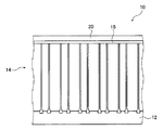
図1に、本発明の放射線画像変換パネルの一例の概念図を示す。
本発明の放射線画像変換パネル10(以下、変換パネル10とする)は、基板12と、蛍光体層14と、蛍光体層14を全面的に覆って封止する保護層20とを有する。また、図示例においては、好ましい態様として、接着層18によって、蛍光体層14と保護層20とが接着されている。
In FIG. 1, the conceptual diagram of an example of the radiographic image conversion panel of this invention is shown.
The radiation image conversion panel 10 (hereinafter referred to as the conversion panel 10) of the present invention includes a
なお、本発明の放射線画像変換パネルは、上記構成に限定はされず、蛍光体層14が、気相堆積法によって形成さた柱状結晶構造を有し、かつ、柱状結晶の柱径分布が後述する条件を満たすものであれば、各種の構成が利用可能である。
例えば、蛍光体層14が十分な耐湿性を有するのであれば、接着層18および保護層20を有さなくてもよく、また、接着層18によって保護層20と蛍光体層14とを接着せずに、基板12(あるいは後述する枠体32)と保護層20とを接着するのみで、保護層20で蛍光体層14を覆って封止してもよい。
The radiation image conversion panel of the present invention is not limited to the above configuration, and the
For example, if the
本発明の変換パネル10において、基板12には、特に限定はななく、公知の放射線画像変換パネルで用いられている各種のものが利用可能である。
一例として、セルロースアセテート、ポリエステル、ポリエチレンテレフタレート、ポリアミド、ポリイミド、トリアセテート、ポリカーボネートなどから形成されるプラスチック板やプラスチックシート(フィルム); 石英ガラス、無アルカリガラス、ソーダガラス、耐熱ガラス(パイレックスTM等)などから形成されるガラス板やガラスシート; アルミニウム、鉄、銅、クロムなどの金属類から形成される金属板や金属シート; このような金属板等の表面に金属酸化物層等の被覆層を形成してなる板やシート; 等が例示される。
また、基板12は、表面に、保護層(基板12の基体を保護する保護層)、輝尽発光光の反射層あるいはさらに反射層の保護層などを有してもよい。この際には、蛍光体層14は、これらの層の上に形成される。
In the
Examples include plastic plates and plastic sheets (films) formed from cellulose acetate, polyester, polyethylene terephthalate, polyamide, polyimide, triacetate, polycarbonate, etc .; quartz glass, alkali-free glass, soda glass, heat-resistant glass (Pyrex ™, etc.), etc. Glass plates and glass sheets formed from: metal plates and metal sheets formed from metals such as aluminum, iron, copper, and chromium; a coating layer such as a metal oxide layer is formed on the surface of such metal plates Examples of such a plate or sheet are as follows.
Further, the
なお、後に詳述するが、本発明の製造方法では、2以上の異なる径の円柱状の凸部を多数有する凹凸状の表面を有し、かつ、最大の凸部の径をR、その他の凸部の径をrとした際に「0.4R≦r≦0.8R」を満たす基板12を用いる。
図1に示す変換パネル10は、この本発明の製造方法によって作製したもので、基板12として、2つの径の異なる凸部が全面的に形成された凹凸状の表面を有する基板12を用いている。
As will be described in detail later, in the manufacturing method of the present invention, the surface has a concavo-convex shape having a large number of cylindrical convex portions having two or more different diameters, and the diameter of the largest convex portion is R. The
A
本発明の変換パネル10において、蛍光体層14は、真空蒸着等の気相堆積法によって形成されたもので、基本的に、互いに独立する柱状結晶によって形成される、柱状結晶構造を有する。
In the
なお、図1に示す変換パネル10においては、基板12の表面から柱状結晶が成長しているが、本発明は、これに限定はされない。
例えば、真空蒸着で形成される蛍光体層、特に輝尽性蛍光体からなる蛍光体層、中でも特に後述するアルカリハライド系輝尽性蛍光体からなる蛍光体層は、蛍光体層14の形成条件(成膜条件)に応じて、当初は結晶が球状に成長して、その後、結晶が球状から柱状に成長して柱状結晶となる場合も多い。この場合には、本発明の変換パネル10は、基板12の表面に球状結晶が凝集してなる球状結晶層を有し、その上に柱状結晶層を有する構成であってもよい。
また、このように球状に結晶が成長する場合には、蛍光体層14の形成条件によっては、柱状結晶が成長する前に、球状結晶が基板12の面方向に融着して塊状(ドメイン)となり、このドメインから結晶が柱状に成長して柱状結晶となる場合も多い。この場合には、本発明の変換パネル10は、基板12の表面に球状結晶が凝集してなる球状結晶層を有し、その上に前記ドメインからなるドメイン層を有し、このドメイン層の上に柱状結晶層を有する構成であってもよい。
In the
For example, a phosphor layer formed by vacuum vapor deposition, particularly a phosphor layer made of a stimulable phosphor, particularly a phosphor layer made of an alkali halide-based stimulable phosphor described later, is a forming condition of the
Further, when the crystal grows in a spherical shape in this way, depending on the formation conditions of the
前述のように、蛍光体層14は、互いに独立した柱状結晶で形成される。ここで、本発明の変換パネル10においては、蛍光体層14を形成する柱状結晶の柱径分布が、2以上のピーク(分布の変化が上昇から下降に転ずる点)を有する。
図示例の変換パネル10は、図2の蛍光体層28の表面(基板12と逆側の面)の模式図に示すように、基本的に、互いに柱径の異なる2種の柱状結晶で形成され、図3に模式的に示すように、柱径分布は2つのピークを有している。
As described above, the
The
真空蒸着等の気相堆積法による蛍光体層、特に、輝尽性蛍光体からなる蛍光体層は、柱状結晶から形成される柱状結晶構造を有する場合が多い。
ここで、気相堆積法で形成される、柱状結晶からなる蛍光体層の柱径分布は、正規分布であり、従って、1つのピークしか有していない。また、前記特許文献1、特許文献3、および特許文献4にも示されるように、従来の変換パネルでは、蛍光体層を形成する柱状結晶の柱径は均一であるのが好ましく、すなわち柱径分布は可能な限り少ない方が好ましいと考えられており、できるだけ柱径分布を持たせないように蛍光体層を作製している。
しかしながら、本発明者は、鋭意検討の結果、柱状結晶からなる蛍光体層は、均一な柱径の柱状結晶で形成される構成、すなわち柱径分布が1つのピークしか有さない状態より、2以上の異なる柱径の柱状結晶が混在する構成、すなわち柱径分布が2以上のピークを有する状態の方が、優れた感度および鮮鋭性(鮮鋭度の高い再生画像)が得られることを見いだした。
A phosphor layer formed by a vapor deposition method such as vacuum evaporation, particularly a phosphor layer made of a stimulable phosphor, often has a columnar crystal structure formed from columnar crystals.
Here, the column diameter distribution of the phosphor layer made of columnar crystals formed by the vapor deposition method is a normal distribution, and thus has only one peak. In addition, as shown in Patent Document 1, Patent Document 3, and Patent Document 4, in the conventional conversion panel, the column diameter of the columnar crystal forming the phosphor layer is preferably uniform, that is, the column diameter. The distribution is considered to be as small as possible, and the phosphor layer is produced so as not to have a column diameter distribution as much as possible.
However, as a result of intensive studies, the present inventor has found that the phosphor layer composed of columnar crystals is formed of columnar crystals having a uniform column diameter, that is, a state where the column diameter distribution has only one peak. It has been found that excellent sensitivity and sharpness (reproduced image with high sharpness) can be obtained in a configuration in which columnar crystals having different column diameters are mixed, that is, in a state where the column diameter distribution has two or more peaks. .
柱径分布が2以上のピークを有することによって、変換パネル10の感度および鮮鋭性が向上する理由は、明らかでは無い。本発明者の検討によれば、このような柱径分布を有することで、2以上の互いに柱径が異なる柱状結晶が混在して、大きな柱径の柱状結晶の間に、小さい柱径の柱状結晶が存在する構成となり、その結果、大きな柱径の柱状結晶によって優れた感度が得られ、かつ、この大きな柱径の柱状結晶の間を柱径の小さい柱状結晶が埋めたような状態となることで、優れた鮮鋭性が得られると推測される。
The reason why the sensitivity and sharpness of the
なお、本発明の変換パネル10において、蛍光体層14を形成する柱状結晶の柱径を直接測定することは、非常に困難である。そのため、本発明においては、一例として、作製した蛍光体層14の表面の電子顕微鏡写真を撮影し、この電子顕微鏡写真上で柱状結晶の柱径を計測して、柱径分布を得ればよい。
また、蛍光体層14の全面で柱径を測定して柱径分布を得るのが好ましいのは、もちろんであるが、必ずしも、その必要はなく、蛍光体層14の表面の任意の4〜5箇所で、1000〜100000μm2程度の面積の電子顕微鏡写真を撮影して、柱径を測定することで、蛍光体層14全面の柱径分布を適正に知見することができる。
柱径分布のピッチ(柱径の刻み幅)にも特に限定はないが、大きすぎると適正な柱径分布が得られず、逆に、小さすぎるとノイズ等の影響が大きくなる可能性が生じるので、一例として、0.1μmピッチで柱径分布を得て、ピークの数を知見するのが好ましい。
なお、柱状結晶の形状(上面(膜の表面側)から見た形状=基板12の面方向の形状)は、必ずしも真円には成らないので、この際には、長径と短径(最長の対角線と最短の対角線)を計り、両者の平均を柱状結晶の柱径(平均柱径=(長径+短径)/2)と見なせばよい。
In the
In addition, it is of course preferable to measure the column diameter over the entire surface of the
The pitch of the column diameter distribution (step size of the column diameter) is not particularly limited, but if it is too large, an appropriate column diameter distribution cannot be obtained. Conversely, if it is too small, the influence of noise or the like may increase. Therefore, as an example, it is preferable to obtain the column diameter distribution at a pitch of 0.1 μm and know the number of peaks.
The shape of the columnar crystal (the shape viewed from the upper surface (the surface side of the film) = the shape in the surface direction of the substrate 12) is not necessarily a perfect circle. In this case, the major axis and minor axis (longest length) The diagonal line and the shortest diagonal line are measured, and the average of the two may be regarded as the column diameter of the columnar crystal (average column diameter = (major axis + minor axis) / 2).
本発明の変換パネル10において、蛍光体層14の柱状結晶の柱径(前記平均柱径)には、特に限定はないが、3〜15μmが好ましい。
ここで、本発明においては、柱状結晶の柱径分布において、最大の柱径のピークの柱径をR、それ以外のピークの柱径をrとした際に、式「0.4R≦r≦0.8R」を満たすのが好ましい。
このような構成を有することにより、柱の独立柱状性(柱間の空隙)を維持し、高柱充填充填による高PSL感度を得られる、等の点で好ましい結果を得ることができる。
In the
Here, in the present invention, in the column diameter distribution of the columnar crystals, when the column diameter of the peak of the maximum column diameter is R and the column diameter of the other peaks is r, the formula “0.4R ≦ r ≦ 0.8R "is preferably satisfied.
By having such a configuration, it is possible to obtain preferable results in terms of maintaining the independent columnarity of the columns (the space between the columns) and obtaining a high PSL sensitivity by high column filling and filling.
また、蛍光体層14の柱状結晶の柱径分布の変動係数にも、特に限定はないが、0.05〜0.3、特に、0.05〜0.2とするのが好ましい。
このような構成を有することにより、柱の独立柱状性(柱間の空隙)を維持し、高柱充填充填による高PSL感度を得すくなる、の点で好ましい結果を得ることができる。
The coefficient of variation of the columnar crystal diameter distribution of the
By having such a configuration, a preferable result can be obtained in that the independent columnarity of the columns (the space between the columns) is maintained and high PSL sensitivity due to the high column filling and filling becomes difficult.
なお、本発明の変換パネル10において、柱径分布のピークの数には、特に限定はなく、2以上であればよい。
但し、ピークの数があまり多いと、柱径分布がピークを1つしか有さない通常の変換パネルと同様になってしまい、本発明の効果が十分に得られない場合があり、柱の独立柱状性(柱間の空隙)を維持した状態で、柱充填を制御しにくくなる、等の不都合が生じる可能性が有るので、ピークの数は、15以下とするのが好ましく、特に、2〜5とするのが好ましい。
In the
However, if the number of peaks is too large, the column diameter distribution will be the same as that of a normal conversion panel having only one peak, and the effects of the present invention may not be sufficiently obtained. Since there is a possibility that inconveniences such as it becomes difficult to control column filling while maintaining columnarity (space between columns), the number of peaks is preferably 15 or less. 5 is preferable.
ここで、本発明においては、ピークに挟まれた谷(分布の変化が下降から上昇に転ずる点)と、この谷を挟む2つのピークとにおいて、谷の高さ(頻度)が、低い方のピークの高さの99%以下となるピーク(谷と、この谷を挟む2つのピークとの関係)を、1以上有するのが好ましい。すなわち、図3で例示すれば、谷と、この谷を挟む2つのピークとにおいて、谷の高さh2が、低い方のピークの高さh1の99%以下となるのが好ましい。言い換えれば、本発明の変換パネル10は、自身の高さに対して99%以下の高さの谷が隣り合わせているピークを、2以上有するのが好ましい。
このような構成を有することにより、柱径分布が2以上のピークを有することで優れた感度および鮮鋭性を得られるという本発明の効果を、より確実かつ安定して発現することができ、好ましい。
Here, in the present invention, the valley height (frequency) between the valley between the peaks (the point at which the distribution changes from falling to rising) and the two peaks that sandwich the valley is the lower one. It is preferable to have one or more peaks (relationship between valleys and two peaks sandwiching the valleys) that are 99% or less of the peak height. That is, as illustrated in FIG. 3, it is preferable that the height h2 of the valley is 99% or less of the height h1 of the lower peak in the valley and the two peaks sandwiching the valley. In other words, the
By having such a configuration, the effect of the present invention in which excellent sensitivity and sharpness can be obtained when the column diameter distribution has two or more peaks can be expressed more reliably and stably, which is preferable. .
蛍光体層14を形成する柱状結晶の形状にも、特に限定はなく、どのような形状であってもよいが、真円に近い形状が好ましく、好ましくは、四角形以上の多角形状、特に、五角形以上の多角形状が好ましい。
さらに、蛍光体層14を形成する柱状結晶の長径と短径との比R(長径/短径=R)の平均が、式「1<R<2」を満たすのが好ましく、特に、「1<R<1.5」を満たすのが好ましい。
The shape of the columnar crystal forming the
Further, the average of the ratio R (major axis / minor axis = R) of the major axis and minor axis of the columnar crystals forming the
蛍光体層14を形成する柱状結晶の長径/短径の比Rが大きいと、蛍光体層14における蛍光体の充填率が不十分になってしまう場合が有り、その結果、十分な基板12と蛍光体層14との密着力が得られない場合が有る。
これに対し、長径/短径の比Rが小さいと、充填率が向上し、その結果、X線吸収能力が向上して、高画質な放射線画像を得ることができる。さらに充填率が高くなることにより、あらゆる方向に対して応力緩和し易くなるため、基板12と蛍光体層14との密着力が向上する。
特に、蛍光体層14を表面から見た際に、五角形以上の柱状結晶が30%以上存在すると、高画質の放射線画像を得ることができ、かつ、優れた基板12と蛍光体層14との密着力を得ることができる。
If the ratio R of the major axis / minor axis of the columnar crystals forming the
On the other hand, when the ratio R of the major axis / minor axis is small, the filling rate is improved. As a result, the X-ray absorption capability is improved, and a high-quality radiation image can be obtained. Furthermore, since the filling rate becomes higher, it becomes easier to relieve stress in all directions, so that the adhesion between the
In particular, when the
なお、このような四角形以上、好ましくは五角形以上の多角形状を有し、さらに、平均長径と平均短径との比Rを満たす柱状結晶からなる蛍光体層14は、蛍光体層14を形成する基板12の表面を十分に清浄化して、かつ、基板表面をプラズマ洗浄するなど、十分な親水性を有する状態として、さらに、蛍光体層14の形成中(成膜中)に、基板12の温度すなわち蛍光体層14の温度をコントロールする、あるいは、蛍光体層14の蒸着温度をコントロールすることにより、形成することができる。たとえば、多角形柱を得るには、基板12表面の凹凸パターンを多角形にする、基板12の温度を100℃以上に制御し、かつ蒸着時に真空度を0.1〜3Paの間で制御するなどがある。
The
本発明の変換パネルにおいて、蛍光体層14の層厚には、特に限定は無いが、100〜1500μm、特に、500〜1000μmが好ましい。
蛍光体層14の厚さを、上記範囲とすることにより、画像鮮鋭度等の点で好ましい。
In the conversion panel of the present invention, the thickness of the
Setting the thickness of the
ここで、本発明の変換パネル10において、蛍光体層14が蛍光体と付活剤とを有する輝尽性蛍光体で有る場合には、蛍光体層14の全てを輝尽性蛍光体で形成してもよいが、好ましくは、下部に実質的に付活剤を含有しない母体領域を形成し、その上に付活剤を含有する輝尽性蛍光体からなる領域を形成するのが好ましい。一例として、輝尽性蛍光体が、付活剤としてEuを含有するCsBr:Euである場合には、母体領域は実質的にCsBrのみから形成され、輝尽性蛍光体からなる領域はCsBr:Euから形成される。なお、付活剤を実質的に含まないとは、付活剤が1.0×10⁻⁶ppm以下であることをいい、好ましくは全く含まないことをいう。
母体領域も、応力緩和層として作用するので、このような構成とすることにより、蛍光体層14と基板12との密着性を、より良好にすることができる。
Here, in the
Since the base region also acts as a stress relaxation layer, the adhesiveness between the
本発明において、蛍光体層14を形成する蛍光体には、特に限定はなく、放射線画像変換パネルに用いられている公知の各種の蛍光体が、各種、利用可能である。
特に、本発明の効果が発現し易い等の点で、蛍光体と付活剤(賦活剤:activator)とを含有する輝尽性蛍光体は、好適であり、中でも特に、特開昭61−72087号公報に開示される、一般式「MIX・aMIIX’2・bMIIIX''3:cA」で示されるアルカリハライド系輝尽性蛍光体が好適に利用される。
(上記式において、MI は、Li,Na,K,RbおよびCsからなる群より選択される少なくとも一種であり、MIIは、Be,Mg,Ca,Sr,Ba,Zn,Cd,CuおよびNiからなる群より選択される少なくとも一種の二価の金属であり、MIIIは、Sc,Y,La,Ce,Pr,Nd,Pm,Sm,Eu,Gd,Tb,Dy,Ho,Er,Tm,Yb,Lu,Al,GaおよびInからなる群より選択される少なくとも一種の三価の金属であり、X、X’およびX''は、F,Cl,BrおよびIからなる群より選択される少なくとも一種であり、Aは、Eu,Tb,Ce,Tm,Dy,Pr,Ho,Nd,Yb,Er,Gd,Lu,Sm,Y,Tl,Na,Ag,Cu,BiおよびMgからなる群より選択される少なくとも一種である。また、0≦a<0.5であり、0≦b<0.5であり、0<c≦0.2である。)
その中でも、優れた輝尽発光特性を有し、かつ、本発明の効果が特に良好に得られる等の点で、MIが、少なくともCsを含み、Xが、少なくともBrを含み、さらに、Aが、EuまたはBiであるアルカリハライド系輝尽性蛍光体は好ましく、その中でも特に、一般式「CsBr:Eu」で示される輝尽性蛍光体が好ましい。
In the present invention, the phosphor forming the
In particular, a stimulable phosphor containing a phosphor and an activator is preferable in that the effect of the present invention is easily manifested. An alkali halide photostimulable phosphor represented by the general formula “M I X.aM II X ′ 2 .bM III X ″ 3 : cA” disclosed in Japanese Patent No. 72087 is suitably used.
(In the above formula, M I is at least one selected from the group consisting of Li, Na, K, Rb and Cs, and M II is Be, Mg, Ca, Sr, Ba, Zn, Cd, Cu and at least one trivalent metal selected from the group consisting of Ni, M III is, Sc, Y, La, Ce , Pr, Nd, Pm, Sm, Eu, Gd, Tb, Dy, Ho, Er, At least one trivalent metal selected from the group consisting of Tm, Yb, Lu, Al, Ga and In, and X, X ′ and X ″ are selected from the group consisting of F, Cl, Br and I A is from Eu, Tb, Ce, Tm, Dy, Pr, Ho, Nd, Yb, Er, Gd, Lu, Sm, Y, Tl, Na, Ag, Cu, Bi, and Mg. At least one selected from the group consisting of . Also, a 0 ≦ a <0.5, a 0 ≦ b <0.5, it is 0 <c ≦ 0.2.)
Among them, M I contains at least Cs, X contains at least Br, and has excellent photostimulated luminescence properties and the effects of the present invention can be obtained particularly well. However, an alkali halide photostimulable phosphor that is Eu or Bi is preferred, and among these, photostimulable phosphors represented by the general formula “CsBr: Eu” are particularly preferred.
また、これ以外にも、米国特許第3,859,527号明細書、特開昭55−12142号、同55−12144号、同55−12145号、同56−116777号、同58−69281号、同58−206678号、同59−38278号、同59−75200号等の各公報に開示される各種の輝尽性蛍光体も、好適に利用可能である。 In addition, U.S. Pat. No. 3,859,527, JP-A-55-12142, 55-12144, 55-12145, 56-116777, 58-69281. 58-206678, 59-38278, 59-75200, and the like, various photostimulable phosphors disclosed in each publication can be suitably used.
なお、本発明は、輝尽性蛍光体の蛍光体層を有する変換パネル10に限定されず、例えば、沃化セシウムなどの蛍光体の柱状結晶からなる蛍光体層を有する放射線シンチレータパネル等、蛍光体の柱状結晶からなる蛍光体層を有する各種の放射線画像変換パネルに、好適に利用可能である。
The present invention is not limited to the
本発明の変換パネル10において、蛍光体層14は、真空蒸着、スパッタリング、CVD(Chemical Vapor Deposition)等の各種の気相堆積法(真空成膜法)で形成される。
中でも、生産性等の点で真空蒸着によって蛍光体層14を形成するのが好ましい。
In the
Among them, it is preferable to form the
また、蛍光体として輝尽性蛍光体を用いる場合には、蛍光体の成膜材料と付活剤の成膜材料とを独立して加熱/蒸発する、二元(多元)の真空蒸着により、蛍光体層14を形成するのが好ましい。
例えば、輝尽性蛍光体として前記CsBr:Euを用いる場合であれば、蛍光体の成膜材料として臭化セシウム(CsBr)を、付活剤の成膜材料として臭化ユーロピウム(EuBrx(xは、通常、2〜3であるが、2が好ましい))を用いる二元の真空蒸着を行なうのが好ましい。
When a stimulable phosphor is used as the phosphor, the phosphor film-forming material and the activator film-forming material are heated / evaporated independently, by binary (multi-element) vacuum deposition, It is preferable to form the
For example, when CsBr: Eu is used as the stimulable phosphor, cesium bromide (CsBr) is used as the phosphor film forming material, and europium bromide (EuBr x (x Is usually 2 to 3, but 2 is preferred) and it is preferred to carry out binary vacuum deposition using
また、蛍光体層14を真空蒸着で形成する際に、真空蒸着における加熱方法には、特に限定はなく、例えば、電子銃等を用いる電子線加熱、または、抵抗加熱で形成されたものでもよい。さらに、多元の真空蒸着を利用する場合には、全ての材料を同様の同じ加熱手段(例えば、電子線加熱)で加熱蒸発してもよく、あるいは、蛍光体の材料は電子線加熱で、微量である付活剤の材料は抵抗加熱で、それぞれ加熱蒸発して形成されてもよい。
In addition, when the
また、蛍光体層114の形成条件(成膜条件)にも、特に限定はなく、用いる気相堆積法の種類、使用する成膜材料、加熱手段等に応じて、適宜、決定すればよい。
ここで、本発明の変換パネル10においては、前述した各種の輝尽性蛍光体、特にアルカリハライド系輝尽性蛍光体、中でも特に前記一般式「CsX:Eu」で示される輝尽性蛍光体、その中でも特にCsBr:Euからなる蛍光体層14を真空蒸着によって形成する場合には、一旦、系内を高い真空度に排気した後、アルゴンガスや窒素ガス等を系内に導入して、0.01〜3Pa程度の真空度(以下、便宜的に中真空とする)とし、この中真空下で抵抗加熱等によって成膜材料を加熱して真空蒸着を行うのが好ましい。
前述のように、本発明の変換パネル10の蛍光体層14は、互いに独立した柱状結晶によって形成されるが、このような中真空下で成膜して得られる蛍光体層14、特に、前記CsBr:Eu等のアルカリハライド系の蛍光体層14は、特に良好な柱状の結晶構造を有し、輝尽発光特性や画像の鮮鋭性等の点で好ましい。
Further, the formation conditions (film formation conditions) of the phosphor layer 114 are not particularly limited, and may be determined as appropriate according to the type of vapor deposition method used, the film formation material used, the heating means, and the like.
Here, in the
As described above, the
ここで、前述のような、柱状結晶の柱径分布が2以上のピークを有する蛍光体層14は、2以上の異なる径の円柱状の凸部を形成してなる凹凸状の表面を有し、かつ、この前記凸部の最大径をR、その他の凸部の径をrとした際に「0.4R≦r≦0.8R」を満たす基板12を用いて、この基板12に真空蒸着等の気相堆積法によって蛍光体層を形成する、本発明の製造方法で安定して作製できる。
また、より確実に蛍光体層14を形成する柱状結晶の柱径分布が2ピーク以上となり、かつ、より好適に柱径分布が2ピーク以上であることの効果を得られる等の点で、基板12の凸部は、目的とする柱径分布に応じた径の凸部がパターン化された状態で形成されるのが好ましく、特に、各径の凸部が、所定の順番で、かつ所定の間隔(ピッチ)で配列された状態で形成されるのが好ましい。
さらに、前述のように、蛍光体層14の柱径分布のピークの数は、15以下であるのが好ましいので、基板12に形成される凸部の径も15種以下、特に、2〜5種であるのが好ましい。
Here, as described above, the
Further, the substrate diameter distribution of the columnar crystals forming the
Furthermore, as described above, the number of peaks in the column diameter distribution of the
互いに独立した柱状結晶を好適に作成するために、多数の凸部を有する基板を用いて、気相堆積法で蛍光体層を形成する技術が知られている。このような蛍光体層の形成では、一般的に、結晶は凸部から優先的に成長し、その結果、好適に、互いに独立した柱状結晶を形成することができる。
例えば、本件出願人による前記特許文献5(特開2004−3955号公報)には、表面に多数の凸部を有する基板(支持体)を用い、この凸部を起点に成長させた柱状結晶のみからなる、互いの界面が明確で光学的に独立した柱状結晶で形成される蛍光体層を有することにより、非常に優れた鮮鋭性を有する変換パネルが開示されている。
In order to suitably create columnar crystals independent of each other, a technique for forming a phosphor layer by a vapor deposition method using a substrate having a large number of convex portions is known. In the formation of such a phosphor layer, in general, crystals preferentially grow from the convex portions, and as a result, columnar crystals independent of each other can be suitably formed.
For example, in the above-mentioned Patent Document 5 (Japanese Patent Laid-Open No. 2004-3955) by the present applicant, only a columnar crystal using a substrate (support) having a large number of protrusions on the surface and growing from the protrusions is used. There is disclosed a conversion panel having a very excellent sharpness by having a phosphor layer formed of columnar crystals having clear interfaces and optically independent interfaces.
ここで、このような凸部から成長した柱状結晶の柱径は、基本的に、凸部の径に依存し、蛍光体層の形成条件が同じであれば、小さな径の凸部から成長した柱状結晶の径が、大きな径の凸部から成長した柱状結晶よりも大きな径となることは、ほとんど無い。
従って、目的とする柱径分布に応じて、互いに径が異なる2種以上の凸部がパターン化して形成された凹凸状の基板12を用いることにより、柱径分布が2以上のピークを有する蛍光体層14を、好適に作製できる。さらに、凸部の最大径Rと、その他の凸部の径rとが「0.4R≦r≦0.8R」を満たすことにより、大きな径の柱状結晶と小さな径の柱状結晶とのバランスも、好適にできる。
なお、本発明において、凸部の径には、特に限定は無いが、凸部の径が大きすぎると、凸部から成長する柱状結晶が、凸部の径に依存せず、凸部に細い柱状結晶が複数本できてしまうため、凸部から成長する柱状結晶が、凸部の径に依存する範囲で、適宜、決定される。
Here, the column diameter of the columnar crystal grown from such a convex portion basically depends on the diameter of the convex portion. If the formation conditions of the phosphor layer are the same, it grows from the convex portion having a small diameter. The diameter of the columnar crystal is almost never larger than that of a columnar crystal grown from a convex portion having a large diameter.
Therefore, by using the concavo-
In the present invention, the diameter of the convex portion is not particularly limited. However, if the diameter of the convex portion is too large, the columnar crystal growing from the convex portion is not dependent on the diameter of the convex portion and is thin in the convex portion. Since a plurality of columnar crystals are formed, the columnar crystal growing from the convex portion is appropriately determined within a range depending on the diameter of the convex portion.
なお、凸部を円柱ではなく、角柱、好ましくは四角柱以上の多角柱状として、サイズ(上面のサイズ)の異なる凸部をパターンニングして形成した基板を用いても、同様に、柱径分布が2以上のピークを有する蛍光体層14を作製できる。
なお、この際において、凸部の柱径Rおよびrは、対角線(正多角形ではない場合は、最長と最短の平均)とすればよい。
Even if a substrate is formed by patterning convex portions having different sizes (upper surface size), the convex portion is not a cylinder but a prism, preferably a quadrangular prism or more, and a column diameter distribution is similarly used. Can produce a
In this case, the column diameters R and r of the protrusions may be diagonal lines (the average of the longest and shortest when not a regular polygon).
あるいは、異なる柱径(サイズ)の凸部を形成するのではなく、同じ柱径の凸部を形成した凹凸状の基板を用いる蛍光体層の形成において、凸部の柱径、凸部のピッチ(中心の間隔)、凸部の間隔、凸部の高さ、凸部の柱径とピッチとの比等を、互いに調整することによって、柱径分布が2以上のピークを有する蛍光体層14を作製することもできる。
ここで、このように凸部のサイズやピッチ、凸部の高さ等を調整して柱径分布が2以上のピークを有する蛍光体層14を作製する場合には、凸部の高さが極めて重要であり、凸部の高さを0.8μm以下とする必要がある。
Alternatively, in forming a phosphor layer using a concavo-convex substrate in which convex portions having the same column diameter are formed instead of forming convex portions having different column diameters (sizes), the column diameter of the convex portions and the pitch of the convex portions The
Here, when the
前述のように、基板12の表面に凸部を有することにより、この凸部が起点となって柱状結晶が成長する。ここで、この凸部の高さが高いほど、柱状結晶の成長の選択性が高くなり、基板12に形成した凸部が0.8μm超、特に1μm以上であると、この凸部のみから結晶が成長する。その結果、特許文献5に示されるように、凸部を起点とする同じ柱径の柱状結晶が、密に形成される。
これに対し、凸部の高さを0.8μm以下とすることにより、凸部に対する柱状結晶の選択性が低くなり、凸部以外の基板表面(凹部)からも柱状結晶が成長する。しかしながら、やはり、柱状結晶の成長の選択性は、凸部の方が高いので、柱状結晶は凸部が優先的に成長する。そのため、凸部を起点に成長する柱状結晶は、凸部以外の基板表面から成長する柱状結晶よりも柱径が太くなる。その結果、凸部から成長した柱状結晶と、それ以外の基板表面から成長した柱状結晶とで柱径が異なる、柱径分布が2以上のピークを有する蛍光体層14を作製することができる。
As described above, by having a convex portion on the surface of the
On the other hand, when the height of the convex portion is 0.8 μm or less, the selectivity of the columnar crystal with respect to the convex portion is lowered, and the columnar crystal grows from the substrate surface (concave portion) other than the convex portion. However, the selectivity of growth of the columnar crystal is still higher in the convex portion, so that the convex portion of the columnar crystal grows preferentially. Therefore, the columnar crystal grown from the convex portion has a larger column diameter than the columnar crystal grown from the substrate surface other than the convex portion. As a result, it is possible to produce the
但し、あまりに凸部の高さが低いと、凸部を有さない基板と同様になってしまうので、凸部の高さは、0.1μm以上とする必要がある。 However, if the height of the convex portion is too low, it becomes the same as the substrate having no convex portion, so the height of the convex portion needs to be 0.1 μm or more.
基板12に、このような凸部(凹凸)を形成する方法には、特に限定はなく、公知の各種の加工方法が利用可能である。
一例として、半導体製造などに用いられているフォトリソグラフィ技術を利用して、フォトレジストで形成する凸部に応じたパターンを形成し、フォトレジストをマスクとするエッチング等によって、基板12に目的とする凸部パターン(凹凸パターン)を形成する方法が好適に例示される。
あるいは、基板12の表面をサンドブラスト処理して、凹凸パターンを形成する方法も、利用可能である。
There is no particular limitation on the method of forming such convex portions (unevenness) on the
As an example, by using a photolithography technique used in semiconductor manufacturing or the like, a pattern corresponding to a convex portion formed with a photoresist is formed, and etching is performed using the photoresist as a mask. A method for forming a convex pattern (uneven pattern) is preferably exemplified.
Alternatively, a method of forming a concavo-convex pattern by sandblasting the surface of the
また、柱状結晶の柱径分布が2以上のピークを有する蛍光体層14の形成方法としては、基板12に温度分布を設けて蛍光体層14を形成する方法も、利用可能である。
一般的に、基板温度が高い方が、太い柱径の柱状結晶が成長する。そのため、例えば、基板が点状の高温部および/または低温部を有する状態で、蛍光体層を形成することにより、柱状結晶の柱径分布が2以上のピークを有する蛍光体層14を形成できる。
基板12に温度分布を持たせる方法としては、各種の方法が利用可能である。一例として、真空蒸着装置などの蛍光体層の形成装置の基板ホルダに、基板の裏面に接触して、基板を加熱あるいは放熱する温度調整手段を設け、基板の裏面、もしくは、ホルダの基板との接触面に凹凸を設けて、ホルダと基板との接触を点接触とすることにより、基板12に温度分布を持たせる方法が例示される。
As a method for forming the
Generally, a columnar crystal having a thick column diameter grows when the substrate temperature is higher. Therefore, for example, by forming the phosphor layer in a state where the substrate has a dotted high temperature portion and / or a low temperature portion, the
Various methods can be used as a method for giving the
このようにして、基板12上に蛍光体層14を形成したら、必要に応じて、アニーリング(熱処理)を行なう。
また、基板12への蛍光体層14の形成に先立ち、プラズマ洗浄等によって基板12の表面を清浄化するのも好ましい。
After the
It is also preferable to clean the surface of the
図示例の変換パネル10は、好ましい態様として、蛍光体層14の表面を全面的に覆って、蛍光体層14を密閉的に封止する保護層20を有する。
The
気相堆積法で形成した蛍光体層、特に、前述のアルカリハライド系の輝尽性蛍光体は、吸湿性が高く、吸湿によって容易に劣化してしまう。
そのため、本発明の変換パネル10においては、蛍光体層の吸湿を防止するために、図1に示すように、防湿性(非水分透過性)を有する保護層20で、蛍光体層14を全面的に覆って、密閉して封止するのが好ましい。
The phosphor layer formed by the vapor deposition method, particularly the above-mentioned alkali halide stimulable phosphor, has high hygroscopicity and easily deteriorates due to moisture absorption.
Therefore, in the
保護層20は、十分な防湿性を有するものであれば、各種のものが利用可能であり、特に限定はない。
一例として、PET(ポリエチレンテレフタレート)フィルム上に、SiO2膜と、SiO2およびPVA(ポリビニルアルコール)のハイブリット層と、SiO2膜との3層を形成してなる保護層20が例示される。なお、このSiO2膜/SiO2およびPVAのハイブリット層/SiO2膜の3層を形成した保護層20において、例えば、SiO2膜は、スパッタリング法を用いて、SiO2とPVAとのハイブリット層は、PVAとSiO2の比率が1:1となるようにゾルゲル法を用いて、それぞれ形成すればよい。
これ以外にも、ガラス板(フィルム)、ポリエチレンテレフタレートやポリカーボネート等の樹脂フィルム、樹脂フィルムにSiO2、Al2O3、SiCなどの無機物質を堆積したフィルム等も好ましく例示される。
As long as the
As an example, PET (polyethylene terephthalate) film, a SiO 2 film, and the hybrid layer of SiO 2 and PVA (polyvinyl alcohol), the
In addition to this, a glass plate (film), a resin film such as polyethylene terephthalate or polycarbonate, a film in which an inorganic substance such as SiO 2 , Al 2 O 3 , or SiC is deposited on the resin film are also preferably exemplified.
本発明の変換パネル10においては、蛍光体層14を保護層20で全面的に覆って、蛍光体層14の全周を囲んで接着層18によって保護層20と基板12とを接着することにより、保護層20で蛍光体層14を全面的に覆って、密閉して封止すればよい。
しかしながら、基板12と保護層20のみならず、図1に示すように、柱状結晶層28の表面にも接着層18を設け、保護層20を柱状結晶層28にも接着するのが、より好ましい。このような構成とすることにより、保護層20の浮き等を防止して、より機械的強度に優れた耐久性の高い変換パネル10を得ることができる。
In the
However, it is more preferable to provide the
保護層20を接着する接着層18には、特に限定は無いく、十分な接着力を有するものが、各種、利用可能である。但し、図示例のように、柱状結晶層28の表面にも接着層18を設ける場合には、接着層18は、輝尽発光光および励起光を十分に透過する光学特性を有するものを用いる必要が有る。
The
また、本発明においては、図4および図5に模式的に示すように、基板12の表面に、蛍光体層14を面方向(基板12の面方向)に囲む枠体32(例えば、四角筒状の枠体)を有し、この枠体32(あるいはさらに蛍光体層14)に保護膜20を接着して、蛍光体層14を全面的に密閉して封止してなる(放射線像)変換パネル30も好ましい。
Further, in the present invention, as schematically shown in FIGS. 4 and 5, a frame 32 (for example, a square cylinder) surrounding the
この変換パネル30を製造する際には、まず、基板12に枠体32を固定する。ここで、図示例においては、好ましい態様として、基板12の表面に溝12aを形成し、この溝12aに枠体32を挿入して、基板12に枠体32を固定する。このような構成を有することにより、枠体32の位置制度を向上できると共に、枠体32の位置決め作業等をより容易にでき、好ましい。
なお、本発明は、これに限定はされず、溝12aを設けずに基板12に枠体32を固定してもよいのは、もちろんである。また、枠体32の固定方法も、接着剤を用いる方法、ハンダを用いる方法、溝12aを有する場合には溝12aに嵌合する方法等、基板12および枠体32の材料や形状に応じた、各種の方法が利用可能である。
When manufacturing the
In addition, this invention is not limited to this, Of course, you may fix the
次いで、マスキングを行なって、真空蒸着等の気相堆積法によって、枠体32で囲まれた領域内に、前述のようにして蛍光体層14を形成する。
蛍光体層14の形成が終了したら、必要に応じてアニーリングを行なった後、枠体32の上に接着層18を形成し、枠体32および蛍光体層14を保護層20で覆って、熱ラミネーション等によって保護層20を枠体32に接着することにより、枠体24と保護層20とで、蛍光体層14を全面的に覆って、密閉して封止して、変換パネル30とする。ここで接着層18は、枠体32の上面のみに設けて、枠体32と保護層20のみを接着してもよいが、図示例のように、蛍光体層14の表面にも接着層18を設け、蛍光体層14と保護層20も、接着層18で接着するのが好ましいのは、先の例と同様である。
このような枠体32を設け、この枠体32に保護層20を接着することにより、保護層20による封止時に、蛍光体層14の表面と保護層20の接着面とを略同一平面状にすることができるので、保護層20による封止を、より容易かつ両結晶層にダメージを与えることなく行なうことが可能になる。
Next, masking is performed, and the
When the formation of the
By providing such a
以上、本発明の放射線画像変換パネルおよび放射線画像変換パネルの製造方法について詳細に説明したが、本発明は上記実施形態に限定はされず、本発明の要旨を逸脱しない範囲において、各種の改良や変更を行ってもよいのは、もちろんである。 The radiation image conversion panel and the method for manufacturing the radiation image conversion panel of the present invention have been described in detail above. However, the present invention is not limited to the above-described embodiment, and various improvements and modifications can be made without departing from the scope of the present invention. Of course, changes may be made.
以下、本発明の具体的実施例を挙げ、本発明をより詳細に説明する。なお、本発明は、以下の実施例に限定されないのは言うまでもない。 Hereinafter, the present invention will be described in more detail with reference to specific examples of the present invention. Needless to say, the present invention is not limited to the following examples.
[実施例1]
付活剤の成膜材料として臭化ユーロピウムを、蛍光体の成膜材料として臭化セシウムを、それぞれ用いる二元の真空蒸着によって、図1に示す蛍光体層14を有する変換パネル10を作製した。
[Example 1]
The
面積450×450mmのアルミニウム製の板(厚さ10mm)を用意した。
このアルミニウム板の表面(蛍光体層の形成面)の全面に、図6(A)に示すように、5μm間隔の格子の交点を中心として、柱径が3.5μmで高さが0.5μmの円柱状の凸部を形成して、基板12とした。なお、凸部(凹凸)は、フォトリソグラフィによって形成した。
An aluminum plate (
As shown in FIG. 6 (A), a column diameter of 3.5 μm and a height of 0.5 μm are formed on the entire surface of the aluminum plate (the surface on which the phosphor layer is formed), with the intersection of 5 μm intervals as the center. The cylindrical convex portion was formed as a
この基板12を真空蒸着装置の基板ホルダにセットし、また、所定位置に各成膜材料をセットし、さらに、成膜領域が基板12の中央の430×430mmとなるように基板12の表面をマスキングした。なお、基板ホルダは、基板を裏面(蛍光体層の非形成面)から加熱する加熱ヒータを有する。
なお、両成膜材料共に、加熱は、タンタル製のルツボと出力6kWのDC電源とを用いる抵抗加熱装置で行った。なお、ルツボの設置位置の上部には、ルツボから蒸発した成膜材料を遮蔽するシャッタが設置されている。また、蛍光体の成膜材料を収容したルツボには、温度測定手段を設けた。
The
In addition, both film-forming materials were heated with a resistance heating apparatus using a tantalum crucible and a 6 kW DC power source. Note that a shutter that shields the film forming material evaporated from the crucible is provided above the crucible installation position. The crucible containing the phosphor film-forming material was provided with temperature measuring means.
基板を基板ホルダにセットした後、真空チャンバを閉塞し、排気を開始した。排気は、ディフュージョンポンプおよびクライオコイルを用いた。なお、シャッタは閉塞状態となっている。
真空度が8×10⁻⁴Paとなった時点で、真空チャンバ内にアルゴンガスを導入して真空度を2.6Paとし、次いで、DC電源を駆動してルツボに通電して、成膜材料を溶解した。なお、臭化セシウムの溶解は670℃で行った。また、臭化ユーロピウムは、臭化ユーロピウムが溶解する温度まで電力を上げて、完全に溶解した後、臭化ユーロピウムが蒸発しない温度まで投与電力を落した。なお、臭化ユーロピウムの溶解のための投与電力は、予め行なった臭化ユーロピウムの溶融実験に応じて制御した。
After setting the substrate on the substrate holder, the vacuum chamber was closed and evacuation was started. For the exhaust, a diffusion pump and a cryocoil were used. Note that the shutter is closed.
When the degree of vacuum reaches 8 × 10 −4 Pa, argon gas is introduced into the vacuum chamber to a degree of vacuum of 2.6 Pa, and then the DC power source is driven to energize the crucible to form a film forming material. Was dissolved. The cesium bromide was dissolved at 670 ° C. Europium bromide increased the power to a temperature at which europium bromide was dissolved, and after complete dissolution, the administration power was reduced to a temperature at which europium bromide did not evaporate. The administration power for dissolution of europium bromide was controlled according to a previously conducted melting experiment of europium bromide.
成膜材料の溶解を開始して60分が経過した時点で、臭化セシウムを充填したルツボに対応するシャッタのみを開放して、基板12の表面に蛍光体層14(母体領域)の蒸着を開始した(すなわち、臭化セシウムの蒸発温度は670℃)。
シャッタの開放と同時に、加熱ヒータによって基板12を160℃に加熱した。また、ルツボに印加する電力は、臭化セシウムの基板12への蒸着速度が6μm/分となるように調整した。
When 60 minutes have elapsed since the dissolution of the film forming material, only the shutter corresponding to the crucible filled with cesium bromide is opened, and the phosphor layer 14 (matrix region) is deposited on the surface of the
Simultaneously with the opening of the shutter, the
層厚が50μmとなった時点で、一旦、シャッタを閉塞して、アルゴンガスの導入量を調整して真空チャンバ内の圧力(Arガス圧)を0.8Paとし、また、予め調べた、蛍光体層におけるEu/Csのモル濃度比が0.001:1となる電力まで、臭化ユーロピウム(そのルツボ)への投与電力を上昇した。
次いで、臭化セシウムおよび臭化ユーロピウムを充填したルツボに対応するシャッタを開放して、蛍光体層14の形成を再開(輝尽性蛍光体の蒸着を開始)した。
When the layer thickness reaches 50 μm, the shutter is once closed, the amount of argon gas introduced is adjusted to set the pressure in the vacuum chamber (Ar gas pressure) to 0.8 Pa, and the fluorescence previously examined The dose power to europium bromide (its crucible) was increased to a power at which the Eu / Cs molar concentration ratio in the body layer was 0.001: 1.
Next, the shutter corresponding to the crucible filled with cesium bromide and europium bromide was opened, and the formation of the
蛍光体層14の層厚が700μmとなった時点で、DC電源を停止してルツボへの通電を停止し、蛍光体層14の形成を終了した。
次いで、真空チャンバ内が大気圧なるまで乾燥した空気を導入し、大気開放状態で状態で放置して蛍光体層の冷却を行い、冷却を終了した後、基板12(変換パネル10)を基板ホルダから取り外して真空チャンバから取り出し、窒素雰囲気下で200℃で2時間のアニーリングを行なって、変換パネルを作製した。
When the thickness of the
Next, dry air is introduced until the inside of the vacuum chamber reaches atmospheric pressure, and the phosphor layer is cooled by leaving it in an open state. After the cooling is finished, the substrate 12 (conversion panel 10) is mounted on the substrate holder. Was removed from the vacuum chamber, and annealed at 200 ° C. for 2 hours in a nitrogen atmosphere to prepare a conversion panel.
得られた変換パネルについて、図7に模式的に示すように、基板12(蛍光体層の形成領域)を縦横に4等分した角部近傍の交点の4点、および、中央の交点(基板中心)を中心に、50×60μmの電子顕微鏡写真を撮影した。撮影した5枚の写真の柱状結晶の柱径(長径と短径との平均柱径)を測定して、柱径分布を得た。柱径分布は、0.1μmピッチ(間隔)で作成し、また、最も高いピークを1とする相対度数で示した。
この変換パネルの電子顕微鏡写真(顕微鏡写真の画像データをプリント出力した画像)の1枚を図8(A)に、柱径分布を図8(B)に、それぞれ示す。図8(B)に示すように、この変換パネルの蛍光体層を形成する柱状結晶の柱径分布は、2つのピークを有している。
With respect to the obtained conversion panel, as schematically shown in FIG. 7, four points of intersections in the vicinity of the corners obtained by dividing the substrate 12 (phosphor layer forming region) into four equal parts in the vertical and horizontal directions, and a central intersection point (substrates) An electron micrograph of 50 × 60 μm was taken centering on (center). The column diameter of the columnar crystals of the five photographs taken (average column diameter of major axis and minor axis) was measured to obtain a column diameter distribution. The column diameter distribution was created at a pitch of 0.1 μm (interval), and indicated by a relative frequency with the highest peak being 1.
One of the electron micrographs (images obtained by printing out image data of micrographs) of this conversion panel is shown in FIG. 8A, and the column diameter distribution is shown in FIG. 8B. As shown in FIG. 8B, the columnar diameter distribution of the columnar crystals forming the phosphor layer of this conversion panel has two peaks.
[実施例2]
基板12に形成した凸部の高さを0.8μmとした以外は、実施例1と全く同様にして変換パネルを作製した。
作製した変換パネルについて、実施例1と全く同様にして柱径分布を得た。この変換パネルの電子顕微鏡写真の1枚を図9(A)に、柱径分布を図9(B)に、それぞれ示す。図9(B)に示すように、この変換パネルの蛍光体層を形成する柱状結晶の柱径分布は、2つのピークを有している。
[Example 2]
A conversion panel was produced in exactly the same manner as in Example 1 except that the height of the convex portions formed on the
For the produced conversion panel, a column diameter distribution was obtained in exactly the same manner as in Example 1. One electron micrograph of this conversion panel is shown in FIG. 9A, and the column diameter distribution is shown in FIG. 9B. As shown in FIG. 9B, the column diameter distribution of the columnar crystals forming the phosphor layer of this conversion panel has two peaks.
[実施例3]
実施例1と同様のアルミニウム板に、図6(B)に示すように、5μm間隔の格子の交点を中心とする柱径(直径)が3.5μmで高さが1μmの円柱状の凸部、および、格子の中心を中心とする柱径が2.5μmで高さが1μmの円柱状の凸部を形成した。
なお、凸部の形成は、実施例1と同様に行なった。
[Example 3]
As shown in FIG. 6 (B), a cylindrical convex portion having a column diameter (diameter) of 3.5 μm and a height of 1 μm centered on the intersection of the lattices at intervals of 5 μm is formed on the same aluminum plate as in Example 1. A columnar convex portion having a column diameter of 2.5 μm and a height of 1 μm centered on the center of the lattice was formed.
The convex portions were formed in the same manner as in Example 1.
この柱径の異なる2種の凸部を形成した基板12を用いた以外は、実施例1と全く同様にして変換パネルを作製した。
作製した変換パネルについて、実施例1と全く同様にして柱径分布を得た。この変換パネルの電子顕微鏡写真の1枚を図10(A)に、柱径分布を図10(B)に、それぞれ示す。図10(B)に示すように、この変換パネルの蛍光体層を形成する柱状結晶の柱径分布は、2つのピークを有している。
A conversion panel was produced in exactly the same manner as in Example 1 except that the
For the produced conversion panel, a column diameter distribution was obtained in exactly the same manner as in Example 1. One of the electron micrographs of this conversion panel is shown in FIG. 10 (A), and the column diameter distribution is shown in FIG. 10 (B). As shown in FIG. 10 (B), the column diameter distribution of the columnar crystals forming the phosphor layer of this conversion panel has two peaks.
[比較例1]
実施例1で用いた面積450×450mmのアルミニウム板を、そのまま基板として用いた(すなわち、基板表面に凸部無し)以外は、実施例1と全く同様にして変換パネルを作製した。
作製した変換パネルについて、実施例1と全く同様にして柱径分布を得た。この変換パネルの電子顕微鏡写真の1枚を図11(A)に、柱径分布を図11(B)に、それぞれ示す。図11(B)に示すように、この変換パネルの蛍光体層を形成する柱状結晶の柱径分布は、1のピークしか有していない。
[Comparative Example 1]
A conversion panel was produced in exactly the same manner as in Example 1 except that the aluminum plate having an area of 450 × 450 mm used in Example 1 was used as it was as a substrate (that is, there was no protrusion on the substrate surface).
For the produced conversion panel, a column diameter distribution was obtained in exactly the same manner as in Example 1. One of the electron micrographs of this conversion panel is shown in FIG. 11A, and the column diameter distribution is shown in FIG. 11B. As shown in FIG. 11 (B), the column diameter distribution of the columnar crystals forming the phosphor layer of this conversion panel has only one peak.
[比較例2]
凸部を形成する格子の間隔を3μmとし、凸部の柱径を2.5μmとし、凸部の高さを1μmとした以外は、実施例1と全く同様にして変換パネルを作製した。
作製した変換パネルについて、実施例1と全く同様にして柱径分布を得た。この変換パネルの電子顕微鏡写真の1枚を図12(A)に、柱径分布を図12(B)に、それぞれ示す。図12(B)に示すように、この変換パネルの蛍光体層を形成する柱状結晶の柱径分布は、1のピークしか有していない。
[Comparative Example 2]
A conversion panel was prepared in exactly the same manner as in Example 1, except that the interval between the lattices forming the convex portions was 3 μm, the column diameter of the convex portions was 2.5 μm, and the height of the convex portions was 1 μm.
For the produced conversion panel, a column diameter distribution was obtained in exactly the same manner as in Example 1. One of the electron micrographs of this conversion panel is shown in FIG. 12 (A), and the column diameter distribution is shown in FIG. 12 (B). As shown in FIG. 12 (B), the column diameter distribution of the columnar crystals forming the phosphor layer of this conversion panel has only one peak.
このようにして得られた実施例1〜3、ならびに、比較例1および2の変換パネルについて、感度(PSL感度(輝尽発光量(Photostimulated Luminescence))、鮮鋭性(MTF)、およびDQE(Detective Quantum Efficiency 検出粒子効率)を測定した。 For the conversion panels of Examples 1 to 3 and Comparative Examples 1 and 2 thus obtained, sensitivity (PSL sensitivity (Photostimulated Luminescence)), sharpness (MTF), and DQE (Detective) Quantum Efficiency (detected particle efficiency) was measured.
[感度]
変換パネル10を遮光性のカセッテに収容して、管電圧80kVpのX線を約1mR照射した。
X線照射後、暗室でカセッテから変換パネルを取り出し、半導体レーザ光(波長660nm:10mW)を励起光として蛍光体層に照射し、蛍光体層が発する輝尽発光光を測定した。なお、輝尽発光光の測定は、励起光カットフィルタ(HOYA(株)製 B410)を通して励起光と輝尽発光光とを分離して、光電子増倍管を用いて輝尽発光光を測定することで行なった。
感度の評価は、比較例1のPSL感度を100とする相対評価で行なった。
[sensitivity]
The
After X-ray irradiation, the conversion panel was taken out from the cassette in a dark room, and the phosphor layer was irradiated with semiconductor laser light (wavelength 660 nm: 10 mW) as excitation light, and the stimulated emission light emitted from the phosphor layer was measured. The stimulated emission light is measured by separating the excitation light and the stimulated emission light through an excitation light cut filter (B410 manufactured by HOYA) and measuring the stimulated emission light using a photomultiplier tube. It was done.
The sensitivity was evaluated by relative evaluation with the PSL sensitivity of Comparative Example 1 being 100.
[鮮鋭度]
変換パネルの表面にMTFチャートを密着した状態で、遮光性のカセッテに収容して、管電圧80kVpのX線を約10mR照射した。
X線照射後、暗室でカセッテから変換パネルを取り出し、放射線画像を読み取った。なお、放射線画像の読み取りは、前記PSL感度の評価における輝尽発光光の測定と同様にして行なった。
得られた放射線画像をディスプレイに再生して、MTFを測定した。なお、MTFは、1LP/1mmの相対値で評価した。
[Sharpness]
With the MTF chart in close contact with the surface of the conversion panel, it was housed in a light-shielding cassette and irradiated with about 10 mR of X-rays with a tube voltage of 80 kVp.
After the X-ray irradiation, the conversion panel was taken out from the cassette in a dark room, and a radiation image was read. The radiographic image was read in the same manner as the measurement of stimulated emission light in the evaluation of the PSL sensitivity.
The obtained radiographic image was reproduced on a display, and MTF was measured. The MTF was evaluated with a relative value of 1 LP / 1 mm.
[DQE]
変換パネル10の表面にMTFチャートを密着した状態で、遮光性のカセッテに収容して、管電圧80kVpのX線を約1mR照射した。X線照射後、暗室でカセッテから変換パネルを取り出し、放射線画像を読み取った。なお、放射線画像の読み取りは、前記PSL感度の評価における輝尽発光光の測定と同様にして行なった。得られた放射線画像をディスプレイに再生して、鮮鋭度(MTF)を測定した。
他方、変換パネル10を遮光性のカセッテに収容して、管電圧80kVpのX線を約1mR照射した。X線照射後、暗室でカセッテから変換パネルを取り出し、先と同様にして放射線画像を読み取った。得られた放射線画像をディスプレイに再生して、粒状値(ウイナースペクトル)を測定した。
得られた鮮鋭度と粒状値から、DQEを算出した。
なお、DQEは、比較例1を100とする、1LP/1mmの時の相対値で評価した。
各測定結果を下記表1に示す。
[DQE]
With the MTF chart in close contact with the surface of the
On the other hand, the
DQE was calculated from the obtained sharpness and granularity value.
The DQE was evaluated as a relative value at 1 LP / 1 mm with Comparative Example 1 as 100.
Each measurement result is shown in Table 1 below.

上記表1に示されるように、蛍光体層を形成する柱状結晶の柱径分布が2つのピークを有する本発明の変換パネルは、柱径分布が1つのピークしか有さない従来の変換パネルである比較例に比して、感度、鮮鋭性、およびDQE(画質)が、共に優れたものであり、すなわち、優れた特性を有する変換パネルである。
以上の結果より、本発明の効果は、明らかである。
As shown in Table 1 above, the conversion panel of the present invention in which the columnar distribution of the columnar crystals forming the phosphor layer has two peaks is a conventional conversion panel in which the columnar distribution has only one peak. Compared with a certain comparative example, sensitivity, sharpness, and DQE (image quality) are all excellent, that is, the conversion panel has excellent characteristics.
From the above results, the effect of the present invention is clear.
10,30 (放射線画像)変換パネル
12 基板
14 蛍光体層
18 接着層
20 保護層
32 枠体
10, 30 (Radiation image)
Claims (5)
前記蛍光体層が、柱状結晶からなるものであり、かつ、この柱状結晶の柱径分布が2以上のピークを有することを特徴とする放射線画像変換パネル。 A radiation image conversion panel having a phosphor layer formed by a vapor deposition method,
The radiation image conversion panel, wherein the phosphor layer is made of a columnar crystal, and the column diameter distribution of the columnar crystal has two or more peaks.
0.4R≦r≦0.8R
である請求項1に記載の放射線画像変換パネル。 Of the peaks of the column diameter distribution, when the column diameter of the peak with the largest column diameter is R, the column diameter r of the other peak is
0.4R ≦ r ≦ 0.8R
The radiation image conversion panel according to claim 1.
Priority Applications (2)
| Application Number | Priority Date | Filing Date | Title |
|---|---|---|---|
| JP2006188911A JP2008014892A (en) | 2006-07-10 | 2006-07-10 | Radiological image conversion panel, and manufacturing method of same |
| US11/822,795 US7491949B2 (en) | 2006-07-10 | 2007-07-10 | Radiation image conversion panel and process for producing the same |
Applications Claiming Priority (1)
| Application Number | Priority Date | Filing Date | Title |
|---|---|---|---|
| JP2006188911A JP2008014892A (en) | 2006-07-10 | 2006-07-10 | Radiological image conversion panel, and manufacturing method of same |
Publications (2)
| Publication Number | Publication Date |
|---|---|
| JP2008014892A true JP2008014892A (en) | 2008-01-24 |
| JP2008014892A5 JP2008014892A5 (en) | 2009-04-09 |
Family
ID=38918328
Family Applications (1)
| Application Number | Title | Priority Date | Filing Date |
|---|---|---|---|
| JP2006188911A Withdrawn JP2008014892A (en) | 2006-07-10 | 2006-07-10 | Radiological image conversion panel, and manufacturing method of same |
Country Status (2)
| Country | Link |
|---|---|
| US (1) | US7491949B2 (en) |
| JP (1) | JP2008014892A (en) |
Cited By (7)
| Publication number | Priority date | Publication date | Assignee | Title |
|---|---|---|---|---|
| JP2011027569A (en) * | 2009-07-27 | 2011-02-10 | Hamamatsu Photonics Kk | Scintillator panel and radiation image sensor |
| CN102551754A (en) * | 2010-11-16 | 2012-07-11 | 佳能株式会社 | Scintillator, radiation detecting apparatus, and radiation imaging apparatus |
| JP2012141297A (en) * | 2010-12-17 | 2012-07-26 | Fujifilm Corp | Radiation imaging apparatus |
| US8436322B2 (en) | 2008-03-31 | 2013-05-07 | Konica Minolta Medical & Graphic, Inc. | Radiation image conversion panel |
| WO2013096050A1 (en) * | 2011-12-22 | 2013-06-27 | Saint-Gobain Ceramics & Plastics, Inc. | Image storage device including storage phosphor powder, method of forming image storage device, and computed radiography apparatus |
| US8637830B2 (en) | 2009-03-13 | 2014-01-28 | Hamamatsu Photonics K.K. | Radiation image conversion panel and method for producing same |
| JP5402933B2 (en) * | 2008-08-28 | 2014-01-29 | コニカミノルタ株式会社 | Radiation image conversion panel and manufacturing method thereof |
Families Citing this family (2)
| Publication number | Priority date | Publication date | Assignee | Title |
|---|---|---|---|---|
| JP2009258056A (en) * | 2008-04-21 | 2009-11-05 | Hamamatsu Photonics Kk | Radiation image converting panel |
| MX2017000681A (en) * | 2014-07-17 | 2018-03-12 | Visual Physics Llc | An improved polymeric sheet material for use in making polymeric security documents such as banknotes. |
Family Cites Families (8)
| Publication number | Priority date | Publication date | Assignee | Title |
|---|---|---|---|---|
| US4437011A (en) * | 1980-06-16 | 1984-03-13 | Tokyo Shibaura Denki Kabushiki Kaisha | Radiation excited phosphor screen and method for manufacturing the same |
| JP2003248097A (en) * | 2002-02-25 | 2003-09-05 | Konica Corp | Radiation image conversion panel and its production method |
| JP2004003955A (en) | 2002-03-25 | 2004-01-08 | Fuji Photo Film Co Ltd | Radiological image converting panel |
| EP1359204A1 (en) | 2002-03-26 | 2003-11-05 | Agfa-Gevaert | Needle-shaped cylindrical storage phosphor crystals |
| JP2003302498A (en) | 2002-04-09 | 2003-10-24 | Fuji Photo Film Co Ltd | Manufacturing method of radiological image conversion panel |
| JP2004233067A (en) | 2003-01-28 | 2004-08-19 | Konica Minolta Holdings Inc | Radiation image conversion panel and method for manufacturing the same |
| JP2005098716A (en) | 2003-09-22 | 2005-04-14 | Konica Minolta Medical & Graphic Inc | Radiological image conversion panel and manufacturing method of radiological image conversion panel |
| JPWO2007060814A1 (en) * | 2005-11-28 | 2009-05-07 | コニカミノルタエムジー株式会社 | Radiation scintillator plate |
-
2006
- 2006-07-10 JP JP2006188911A patent/JP2008014892A/en not_active Withdrawn
-
2007
- 2007-07-10 US US11/822,795 patent/US7491949B2/en not_active Expired - Fee Related
Cited By (11)
| Publication number | Priority date | Publication date | Assignee | Title |
|---|---|---|---|---|
| US8436322B2 (en) | 2008-03-31 | 2013-05-07 | Konica Minolta Medical & Graphic, Inc. | Radiation image conversion panel |
| JP5477283B2 (en) * | 2008-03-31 | 2014-04-23 | コニカミノルタ株式会社 | Radiation image conversion panel |
| JP5402933B2 (en) * | 2008-08-28 | 2014-01-29 | コニカミノルタ株式会社 | Radiation image conversion panel and manufacturing method thereof |
| US8637830B2 (en) | 2009-03-13 | 2014-01-28 | Hamamatsu Photonics K.K. | Radiation image conversion panel and method for producing same |
| JP5469158B2 (en) * | 2009-03-13 | 2014-04-09 | 浜松ホトニクス株式会社 | Radiation image conversion panel and manufacturing method thereof |
| KR101585286B1 (en) | 2009-03-13 | 2016-01-13 | 하마마츠 포토닉스 가부시키가이샤 | Radiation image conversion panel and method for producing same |
| JP2011027569A (en) * | 2009-07-27 | 2011-02-10 | Hamamatsu Photonics Kk | Scintillator panel and radiation image sensor |
| CN102551754A (en) * | 2010-11-16 | 2012-07-11 | 佳能株式会社 | Scintillator, radiation detecting apparatus, and radiation imaging apparatus |
| JP2012141297A (en) * | 2010-12-17 | 2012-07-26 | Fujifilm Corp | Radiation imaging apparatus |
| WO2013096050A1 (en) * | 2011-12-22 | 2013-06-27 | Saint-Gobain Ceramics & Plastics, Inc. | Image storage device including storage phosphor powder, method of forming image storage device, and computed radiography apparatus |
| US9029820B2 (en) | 2011-12-22 | 2015-05-12 | Saint-Gobain Ceramics & Plastics, Inc. | Image storage device including storage phosphor powder, method of forming image storage device, and computed radiography apparatus |
Also Published As
| Publication number | Publication date |
|---|---|
| US20080006780A1 (en) | 2008-01-10 |
| US7491949B2 (en) | 2009-02-17 |
Similar Documents
| Publication | Publication Date | Title |
|---|---|---|
| JP2008014892A (en) | Radiological image conversion panel, and manufacturing method of same | |
| US6835940B2 (en) | Radiation image conversion panel | |
| JP2007232619A (en) | Radiological image conversion panel, and manufacturing method of same | |
| JP2007315866A (en) | Radiation image conversion panel and method for manufacturing it | |
| JP3987469B2 (en) | Radiation image conversion panel | |
| JP2006250909A (en) | Radiation image conversion panel | |
| JP3130633B2 (en) | Manufacturing method of radiation image conversion panel | |
| US7420186B2 (en) | Phosphor panel | |
| US20070096041A1 (en) | Stimulable phosphor panel and method of producing stimulable phosphor panel | |
| JP2010014581A (en) | Manufacturing method for radiographic image conversion panel | |
| JP2010014469A (en) | Manufacturing method of radiographic image conversion panel | |
| JP2006098241A (en) | Radiation image conversion panel | |
| JP2006271700A (en) | Radiographic image conversion panel and radiographic diagnostic imaging system | |
| JP5119572B2 (en) | Radiation image conversion panel and manufacturing method thereof | |
| JP2008051807A (en) | Radiation image conversion panel, and method of manufacturing radiation image conversion panel | |
| JPH05249298A (en) | Radiation image conversion pannel | |
| US7183561B2 (en) | Radiation image conversion panel and manufacturing method thereof | |
| JP2006267013A (en) | Stimulable phosphor panel, and manufacturing method for stimulable phosphor panel | |
| JP2004233343A (en) | Radiological image conversion panel | |
| JP2006300647A (en) | Phosphor panel manufacturing method | |
| JP3164598B2 (en) | Manufacturing method of radiation image conversion panel | |
| JP2007298464A (en) | Radiographic image conversion panel, and manufacturing method for radiographic image conversion panel | |
| JP2003232897A (en) | Manufacturing method of radiation image conversion panel | |
| JP2006292509A (en) | Radiological image conversion panel | |
| JP2005315860A (en) | Stimulable phosphor panel and stimulable phosphor panel manufacturing method |
Legal Events
| Date | Code | Title | Description |
|---|---|---|---|
| RD04 | Notification of resignation of power of attorney |
Free format text: JAPANESE INTERMEDIATE CODE: A7424 Effective date: 20080717 |
|
| A521 | Written amendment |
Free format text: JAPANESE INTERMEDIATE CODE: A523 Effective date: 20090223 |
|
| A621 | Written request for application examination |
Free format text: JAPANESE INTERMEDIATE CODE: A621 Effective date: 20090223 |
|
| A761 | Written withdrawal of application |
Free format text: JAPANESE INTERMEDIATE CODE: A761 Effective date: 20090525 |