JP2007536752A - Shielding electronic device and manufacturing method thereof - Google Patents
Shielding electronic device and manufacturing method thereof Download PDFInfo
- Publication number
- JP2007536752A JP2007536752A JP2007511981A JP2007511981A JP2007536752A JP 2007536752 A JP2007536752 A JP 2007536752A JP 2007511981 A JP2007511981 A JP 2007511981A JP 2007511981 A JP2007511981 A JP 2007511981A JP 2007536752 A JP2007536752 A JP 2007536752A
- Authority
- JP
- Japan
- Prior art keywords
- layer
- shielding
- electronic device
- perturbation
- shielding layer
- Prior art date
- Legal status (The legal status is an assumption and is not a legal conclusion. Google has not performed a legal analysis and makes no representation as to the accuracy of the status listed.)
- Pending
Links
Images


Classifications
-
- G—PHYSICS
- G06—COMPUTING; CALCULATING OR COUNTING
- G06K—GRAPHICAL DATA READING; PRESENTATION OF DATA; RECORD CARRIERS; HANDLING RECORD CARRIERS
- G06K19/00—Record carriers for use with machines and with at least a part designed to carry digital markings
- G06K19/06—Record carriers for use with machines and with at least a part designed to carry digital markings characterised by the kind of the digital marking, e.g. shape, nature, code
- G06K19/067—Record carriers with conductive marks, printed circuits or semiconductor circuit elements, e.g. credit or identity cards also with resonating or responding marks without active components
- G06K19/07—Record carriers with conductive marks, printed circuits or semiconductor circuit elements, e.g. credit or identity cards also with resonating or responding marks without active components with integrated circuit chips
- G06K19/077—Constructional details, e.g. mounting of circuits in the carrier
- G06K19/0772—Physical layout of the record carrier
- G06K19/07735—Physical layout of the record carrier the record carrier comprising means for protecting against electrostatic discharge
-
- G—PHYSICS
- G06—COMPUTING; CALCULATING OR COUNTING
- G06K—GRAPHICAL DATA READING; PRESENTATION OF DATA; RECORD CARRIERS; HANDLING RECORD CARRIERS
- G06K19/00—Record carriers for use with machines and with at least a part designed to carry digital markings
- G06K19/06—Record carriers for use with machines and with at least a part designed to carry digital markings characterised by the kind of the digital marking, e.g. shape, nature, code
- G06K19/067—Record carriers with conductive marks, printed circuits or semiconductor circuit elements, e.g. credit or identity cards also with resonating or responding marks without active components
- G06K19/07—Record carriers with conductive marks, printed circuits or semiconductor circuit elements, e.g. credit or identity cards also with resonating or responding marks without active components with integrated circuit chips
- G06K19/077—Constructional details, e.g. mounting of circuits in the carrier
- G06K19/07743—External electrical contacts
-
- H—ELECTRICITY
- H01—ELECTRIC ELEMENTS
- H01L—SEMICONDUCTOR DEVICES NOT COVERED BY CLASS H10
- H01L23/00—Details of semiconductor or other solid state devices
- H01L23/48—Arrangements for conducting electric current to or from the solid state body in operation, e.g. leads, terminal arrangements ; Selection of materials therefor
- H01L23/488—Arrangements for conducting electric current to or from the solid state body in operation, e.g. leads, terminal arrangements ; Selection of materials therefor consisting of soldered or bonded constructions
- H01L23/498—Leads, i.e. metallisations or lead-frames on insulating substrates, e.g. chip carriers
-
- H—ELECTRICITY
- H01—ELECTRIC ELEMENTS
- H01L—SEMICONDUCTOR DEVICES NOT COVERED BY CLASS H10
- H01L23/00—Details of semiconductor or other solid state devices
- H01L23/552—Protection against radiation, e.g. light or electromagnetic waves
-
- H—ELECTRICITY
- H01—ELECTRIC ELEMENTS
- H01L—SEMICONDUCTOR DEVICES NOT COVERED BY CLASS H10
- H01L2224/00—Indexing scheme for arrangements for connecting or disconnecting semiconductor or solid-state bodies and methods related thereto as covered by H01L24/00
- H01L2224/01—Means for bonding being attached to, or being formed on, the surface to be connected, e.g. chip-to-package, die-attach, "first-level" interconnects; Manufacturing methods related thereto
- H01L2224/26—Layer connectors, e.g. plate connectors, solder or adhesive layers; Manufacturing methods related thereto
- H01L2224/31—Structure, shape, material or disposition of the layer connectors after the connecting process
- H01L2224/32—Structure, shape, material or disposition of the layer connectors after the connecting process of an individual layer connector
- H01L2224/3201—Structure
- H01L2224/32012—Structure relative to the bonding area, e.g. bond pad
- H01L2224/32014—Structure relative to the bonding area, e.g. bond pad the layer connector being smaller than the bonding area, e.g. bond pad
-
- H—ELECTRICITY
- H01—ELECTRIC ELEMENTS
- H01L—SEMICONDUCTOR DEVICES NOT COVERED BY CLASS H10
- H01L2224/00—Indexing scheme for arrangements for connecting or disconnecting semiconductor or solid-state bodies and methods related thereto as covered by H01L24/00
- H01L2224/01—Means for bonding being attached to, or being formed on, the surface to be connected, e.g. chip-to-package, die-attach, "first-level" interconnects; Manufacturing methods related thereto
- H01L2224/26—Layer connectors, e.g. plate connectors, solder or adhesive layers; Manufacturing methods related thereto
- H01L2224/31—Structure, shape, material or disposition of the layer connectors after the connecting process
- H01L2224/32—Structure, shape, material or disposition of the layer connectors after the connecting process of an individual layer connector
- H01L2224/321—Disposition
- H01L2224/32151—Disposition the layer connector connecting between a semiconductor or solid-state body and an item not being a semiconductor or solid-state body, e.g. chip-to-substrate, chip-to-passive
- H01L2224/32221—Disposition the layer connector connecting between a semiconductor or solid-state body and an item not being a semiconductor or solid-state body, e.g. chip-to-substrate, chip-to-passive the body and the item being stacked
- H01L2224/32225—Disposition the layer connector connecting between a semiconductor or solid-state body and an item not being a semiconductor or solid-state body, e.g. chip-to-substrate, chip-to-passive the body and the item being stacked the item being non-metallic, e.g. insulating substrate with or without metallisation
-
- H—ELECTRICITY
- H01—ELECTRIC ELEMENTS
- H01L—SEMICONDUCTOR DEVICES NOT COVERED BY CLASS H10
- H01L2224/00—Indexing scheme for arrangements for connecting or disconnecting semiconductor or solid-state bodies and methods related thereto as covered by H01L24/00
- H01L2224/01—Means for bonding being attached to, or being formed on, the surface to be connected, e.g. chip-to-package, die-attach, "first-level" interconnects; Manufacturing methods related thereto
- H01L2224/42—Wire connectors; Manufacturing methods related thereto
- H01L2224/44—Structure, shape, material or disposition of the wire connectors prior to the connecting process
- H01L2224/45—Structure, shape, material or disposition of the wire connectors prior to the connecting process of an individual wire connector
- H01L2224/45001—Core members of the connector
- H01L2224/45099—Material
- H01L2224/451—Material with a principal constituent of the material being a metal or a metalloid, e.g. boron (B), silicon (Si), germanium (Ge), arsenic (As), antimony (Sb), tellurium (Te) and polonium (Po), and alloys thereof
- H01L2224/45138—Material with a principal constituent of the material being a metal or a metalloid, e.g. boron (B), silicon (Si), germanium (Ge), arsenic (As), antimony (Sb), tellurium (Te) and polonium (Po), and alloys thereof the principal constituent melting at a temperature of greater than or equal to 950°C and less than 1550°C
- H01L2224/45144—Gold (Au) as principal constituent
-
- H—ELECTRICITY
- H01—ELECTRIC ELEMENTS
- H01L—SEMICONDUCTOR DEVICES NOT COVERED BY CLASS H10
- H01L2224/00—Indexing scheme for arrangements for connecting or disconnecting semiconductor or solid-state bodies and methods related thereto as covered by H01L24/00
- H01L2224/01—Means for bonding being attached to, or being formed on, the surface to be connected, e.g. chip-to-package, die-attach, "first-level" interconnects; Manufacturing methods related thereto
- H01L2224/42—Wire connectors; Manufacturing methods related thereto
- H01L2224/47—Structure, shape, material or disposition of the wire connectors after the connecting process
- H01L2224/48—Structure, shape, material or disposition of the wire connectors after the connecting process of an individual wire connector
- H01L2224/4805—Shape
- H01L2224/4809—Loop shape
- H01L2224/48091—Arched
-
- H—ELECTRICITY
- H01—ELECTRIC ELEMENTS
- H01L—SEMICONDUCTOR DEVICES NOT COVERED BY CLASS H10
- H01L2224/00—Indexing scheme for arrangements for connecting or disconnecting semiconductor or solid-state bodies and methods related thereto as covered by H01L24/00
- H01L2224/01—Means for bonding being attached to, or being formed on, the surface to be connected, e.g. chip-to-package, die-attach, "first-level" interconnects; Manufacturing methods related thereto
- H01L2224/42—Wire connectors; Manufacturing methods related thereto
- H01L2224/47—Structure, shape, material or disposition of the wire connectors after the connecting process
- H01L2224/48—Structure, shape, material or disposition of the wire connectors after the connecting process of an individual wire connector
- H01L2224/484—Connecting portions
- H01L2224/48463—Connecting portions the connecting portion on the bonding area of the semiconductor or solid-state body being a ball bond
-
- H—ELECTRICITY
- H01—ELECTRIC ELEMENTS
- H01L—SEMICONDUCTOR DEVICES NOT COVERED BY CLASS H10
- H01L2224/00—Indexing scheme for arrangements for connecting or disconnecting semiconductor or solid-state bodies and methods related thereto as covered by H01L24/00
- H01L2224/73—Means for bonding being of different types provided for in two or more of groups H01L2224/10, H01L2224/18, H01L2224/26, H01L2224/34, H01L2224/42, H01L2224/50, H01L2224/63, H01L2224/71
- H01L2224/732—Location after the connecting process
- H01L2224/73251—Location after the connecting process on different surfaces
- H01L2224/73265—Layer and wire connectors
-
- H—ELECTRICITY
- H01—ELECTRIC ELEMENTS
- H01L—SEMICONDUCTOR DEVICES NOT COVERED BY CLASS H10
- H01L23/00—Details of semiconductor or other solid state devices
- H01L23/48—Arrangements for conducting electric current to or from the solid state body in operation, e.g. leads, terminal arrangements ; Selection of materials therefor
- H01L23/488—Arrangements for conducting electric current to or from the solid state body in operation, e.g. leads, terminal arrangements ; Selection of materials therefor consisting of soldered or bonded constructions
- H01L23/498—Leads, i.e. metallisations or lead-frames on insulating substrates, e.g. chip carriers
- H01L23/49855—Leads, i.e. metallisations or lead-frames on insulating substrates, e.g. chip carriers for flat-cards, e.g. credit cards
-
- H—ELECTRICITY
- H01—ELECTRIC ELEMENTS
- H01L—SEMICONDUCTOR DEVICES NOT COVERED BY CLASS H10
- H01L24/00—Arrangements for connecting or disconnecting semiconductor or solid-state bodies; Methods or apparatus related thereto
- H01L24/01—Means for bonding being attached to, or being formed on, the surface to be connected, e.g. chip-to-package, die-attach, "first-level" interconnects; Manufacturing methods related thereto
- H01L24/42—Wire connectors; Manufacturing methods related thereto
- H01L24/44—Structure, shape, material or disposition of the wire connectors prior to the connecting process
- H01L24/45—Structure, shape, material or disposition of the wire connectors prior to the connecting process of an individual wire connector
-
- H—ELECTRICITY
- H01—ELECTRIC ELEMENTS
- H01L—SEMICONDUCTOR DEVICES NOT COVERED BY CLASS H10
- H01L24/00—Arrangements for connecting or disconnecting semiconductor or solid-state bodies; Methods or apparatus related thereto
- H01L24/01—Means for bonding being attached to, or being formed on, the surface to be connected, e.g. chip-to-package, die-attach, "first-level" interconnects; Manufacturing methods related thereto
- H01L24/42—Wire connectors; Manufacturing methods related thereto
- H01L24/47—Structure, shape, material or disposition of the wire connectors after the connecting process
- H01L24/48—Structure, shape, material or disposition of the wire connectors after the connecting process of an individual wire connector
-
- H—ELECTRICITY
- H01—ELECTRIC ELEMENTS
- H01L—SEMICONDUCTOR DEVICES NOT COVERED BY CLASS H10
- H01L2924/00—Indexing scheme for arrangements or methods for connecting or disconnecting semiconductor or solid-state bodies as covered by H01L24/00
- H01L2924/0001—Technical content checked by a classifier
- H01L2924/00014—Technical content checked by a classifier the subject-matter covered by the group, the symbol of which is combined with the symbol of this group, being disclosed without further technical details
-
- H—ELECTRICITY
- H01—ELECTRIC ELEMENTS
- H01L—SEMICONDUCTOR DEVICES NOT COVERED BY CLASS H10
- H01L2924/00—Indexing scheme for arrangements or methods for connecting or disconnecting semiconductor or solid-state bodies as covered by H01L24/00
- H01L2924/01—Chemical elements
- H01L2924/01013—Aluminum [Al]
-
- H—ELECTRICITY
- H01—ELECTRIC ELEMENTS
- H01L—SEMICONDUCTOR DEVICES NOT COVERED BY CLASS H10
- H01L2924/00—Indexing scheme for arrangements or methods for connecting or disconnecting semiconductor or solid-state bodies as covered by H01L24/00
- H01L2924/01—Chemical elements
- H01L2924/01019—Potassium [K]
-
- H—ELECTRICITY
- H01—ELECTRIC ELEMENTS
- H01L—SEMICONDUCTOR DEVICES NOT COVERED BY CLASS H10
- H01L2924/00—Indexing scheme for arrangements or methods for connecting or disconnecting semiconductor or solid-state bodies as covered by H01L24/00
- H01L2924/01—Chemical elements
- H01L2924/0102—Calcium [Ca]
-
- H—ELECTRICITY
- H01—ELECTRIC ELEMENTS
- H01L—SEMICONDUCTOR DEVICES NOT COVERED BY CLASS H10
- H01L2924/00—Indexing scheme for arrangements or methods for connecting or disconnecting semiconductor or solid-state bodies as covered by H01L24/00
- H01L2924/01—Chemical elements
- H01L2924/01057—Lanthanum [La]
-
- H—ELECTRICITY
- H01—ELECTRIC ELEMENTS
- H01L—SEMICONDUCTOR DEVICES NOT COVERED BY CLASS H10
- H01L2924/00—Indexing scheme for arrangements or methods for connecting or disconnecting semiconductor or solid-state bodies as covered by H01L24/00
- H01L2924/01—Chemical elements
- H01L2924/01077—Iridium [Ir]
-
- H—ELECTRICITY
- H01—ELECTRIC ELEMENTS
- H01L—SEMICONDUCTOR DEVICES NOT COVERED BY CLASS H10
- H01L2924/00—Indexing scheme for arrangements or methods for connecting or disconnecting semiconductor or solid-state bodies as covered by H01L24/00
- H01L2924/01—Chemical elements
- H01L2924/01079—Gold [Au]
-
- H—ELECTRICITY
- H01—ELECTRIC ELEMENTS
- H01L—SEMICONDUCTOR DEVICES NOT COVERED BY CLASS H10
- H01L2924/00—Indexing scheme for arrangements or methods for connecting or disconnecting semiconductor or solid-state bodies as covered by H01L24/00
- H01L2924/10—Details of semiconductor or other solid state devices to be connected
- H01L2924/11—Device type
- H01L2924/14—Integrated circuits
-
- H—ELECTRICITY
- H01—ELECTRIC ELEMENTS
- H01L—SEMICONDUCTOR DEVICES NOT COVERED BY CLASS H10
- H01L2924/00—Indexing scheme for arrangements or methods for connecting or disconnecting semiconductor or solid-state bodies as covered by H01L24/00
- H01L2924/15—Details of package parts other than the semiconductor or other solid state devices to be connected
- H01L2924/161—Cap
- H01L2924/1615—Shape
- H01L2924/16152—Cap comprising a cavity for hosting the device, e.g. U-shaped cap
-
- H—ELECTRICITY
- H01—ELECTRIC ELEMENTS
- H01L—SEMICONDUCTOR DEVICES NOT COVERED BY CLASS H10
- H01L2924/00—Indexing scheme for arrangements or methods for connecting or disconnecting semiconductor or solid-state bodies as covered by H01L24/00
- H01L2924/15—Details of package parts other than the semiconductor or other solid state devices to be connected
- H01L2924/181—Encapsulation
-
- H—ELECTRICITY
- H01—ELECTRIC ELEMENTS
- H01L—SEMICONDUCTOR DEVICES NOT COVERED BY CLASS H10
- H01L2924/00—Indexing scheme for arrangements or methods for connecting or disconnecting semiconductor or solid-state bodies as covered by H01L24/00
- H01L2924/30—Technical effects
- H01L2924/301—Electrical effects
- H01L2924/3025—Electromagnetic shielding
Landscapes
- Engineering & Computer Science (AREA)
- Physics & Mathematics (AREA)
- Computer Hardware Design (AREA)
- Microelectronics & Electronic Packaging (AREA)
- General Physics & Mathematics (AREA)
- Theoretical Computer Science (AREA)
- Power Engineering (AREA)
- Condensed Matter Physics & Semiconductors (AREA)
- Toxicology (AREA)
- Electromagnetism (AREA)
- Health & Medical Sciences (AREA)
- Shielding Devices Or Components To Electric Or Magnetic Fields (AREA)
- Thin Magnetic Films (AREA)
- Regulation Of General Use Transformers (AREA)
- Insulated Conductors (AREA)
- Details Of Indoor Wiring (AREA)
- Other Surface Treatments For Metallic Materials (AREA)
Abstract
Description
本発明は、保護すべき少なくとも一つの組立電子部品を有する遮蔽電子装置に関するものである。さらに、本発明は、かかる遮蔽電子部品の製造方法に関する。 The present invention relates to a shielded electronic device having at least one assembled electronic component to be protected. Furthermore, the present invention relates to a method for manufacturing such a shielded electronic component.
さらに具体的には、本発明は、集積回路(IC)、具体的には暗号−演算処理装置などの能動組立電子部品を有するとともに外部交信のための電気接続端子を有する扁平な携帯用電子装置の保護に関する。 More specifically, the present invention relates to a flat portable electronic device having an active assembly electronic component such as an integrated circuit (IC), specifically a cryptographic-arithmetic processing device, and having an electrical connection terminal for external communication. Concerning protection.
前記製品においては、ICの配線内あるいは電子装置の部品間を循環する電流によって、作動周波数に伴って低周波数から数ギガヘルツの周波数までの範囲の周波数の磁場が形成される。 In the product, a magnetic field having a frequency ranging from a low frequency to a frequency of several gigahertz is formed according to the operating frequency by the current circulating in the wiring of the IC or between the components of the electronic device.
前記磁場を磁気センサによって近距離測定すれば、循環電流が直接検出され、それによって前記ICの現場での活動が検出される。それ故、不正な者が前記電子装置の活動を電磁的に検出し、機密情報を入手することが可能である。 If the magnetic field is measured at a short distance by a magnetic sensor, the circulating current is directly detected, thereby detecting the activity of the IC in the field. Therefore, an unauthorized person can electromagnetically detect the activity of the electronic device and obtain confidential information.
本発明は、上記事情に鑑みてなされたものであって、その目的は、保護すべき電子組立部品を有し、扁平な携帯用製品に組み込まれる電子装置の無線高周波の放出を不正な者が検出することを防ぐことにある。 The present invention has been made in view of the above circumstances, and an object thereof is to have an unauthorized person emit radio-frequency waves of an electronic device that has an electronic assembly part to be protected and is incorporated in a flat portable product. It is to prevent detection.
本発明の他の目的は、電子装置の能動部品が光および赤外線によって改ざんされることから電子装置を保護することにある。 Another object of the present invention is to protect electronic devices from being tampered with by active light and infrared rays.
本発明のさらに他の目的は、化学的腐食またはイオン腐食による剥離に対する高い機械耐性を有する電子装置を提供することにある。 It is still another object of the present invention to provide an electronic device having high mechanical resistance against peeling due to chemical corrosion or ionic corrosion.
前記課題を解決するために、本発明にかかる遮蔽電子装置は、保護すべき少なくとも一つの組立電子部品を有し、上面、下面、および外部交信用の電気接続端子を有する遮蔽電子装置であって、前記上面下面の少なくとも一つと、前記組立電子部品から放出する電磁(EM)および/または高周波(RF)電界に対抗する少なくとも一つの遮蔽層とを有し、前記遮蔽層が500を超える大きさの高い非透磁率μrを有する軟磁性材料からなる少なくとも一つの第1の層を有し、前記遮蔽層が機械的研磨や化学的腐食に良好な耐性を示す機械的硬質層である追加の外層をさらに有し、前記遮蔽層が、前記上面および下面の少なくとも一つの、外部装置と接続する前記電気接続端子を設けるための予め設定された領域を除いたほぼ全表面上に設けられていることを特徴とする。 In order to solve the above-mentioned problems, a shielding electronic device according to the present invention is a shielding electronic device having at least one assembly electronic component to be protected, and having an upper surface, a lower surface, and an electrical connection terminal for external communication. And at least one of the upper and lower surfaces and at least one shielding layer against electromagnetic (EM) and / or radio frequency (RF) electric fields emitted from the assembled electronic component, the shielding layer having a size exceeding 500. a high relative has at least one first layer made of soft magnetic material with a magnetic permeability mu r, add the shielding layer is a mechanically hard layer exhibiting a good resistance to mechanical polishing or chemical etching The shielding layer is provided on substantially the entire surface excluding a preset region for providing the electrical connection terminal connected to an external device, at least one of the upper surface and the lower surface. It is characterized by being.
前記保護すべき組立電子部品が少なくとも一つの集積回路を有してもよい。 The assembly electronic component to be protected may comprise at least one integrated circuit.
前記電気接続端子は、好ましくは、前記保護すべき組立電子部品の周縁部分に設けられる。 The electrical connection terminal is preferably provided at a peripheral portion of the assembly electronic component to be protected.
少なくとも一つの軟磁性層を有する前記遮蔽層は、前記電磁RFおよびHF電界を導き、外部での検出を防ぐ遮蔽効果を有する。 The shielding layer having at least one soft magnetic layer has a shielding effect that guides the electromagnetic RF and HF electric fields and prevents detection outside.
前記遮蔽層は、さらに、赤外、可視、および近紫外周波数領域の光の透過を遮断する。 The shielding layer further blocks transmission of light in the infrared, visible, and near ultraviolet frequency regions.
前記遮蔽層の組成は、化学的腐食およびイオン腐食に最大限の耐性を有する様に選択されても良い。 The composition of the shielding layer may be selected to have maximum resistance to chemical and ionic corrosion.
好ましくは、前記遮蔽層の第1の層は、Fe、NiまたはCoを含む合金から構成され、さらに具体的には、NiFe合金、CoNi合金、CoZr合金のいずれかの合金から構成される。 Preferably, the first layer of the shielding layer is made of an alloy containing Fe, Ni, or Co, and more specifically, is made of an alloy of NiFe alloy, CoNi alloy, or CoZr alloy.
前記第1の層の厚みは、2〜40μm、好ましくは10〜30μmである。 The thickness of the first layer is 2 to 40 μm, preferably 10 to 30 μm.
前記遮蔽層は、前記保護すべき組立電子部品と前記第1の層との間に堆積されたTiまたは酸化チタンからなるシード層をさらに有してもよい。 The shielding layer may further include a seed layer made of Ti or titanium oxide deposited between the assembled electronic component to be protected and the first layer.
前記シード層の厚みは、8〜100μm、好ましくは10〜20μmである。 The seed layer has a thickness of 8 to 100 μm, preferably 10 to 20 μm.
前記シード層は、好ましくは、機械的研磨や化学的腐食に対して良好な耐性を示す機械的硬質層である追加の外層をさらに有しても良い。 The seed layer may further comprise an additional outer layer, which is preferably a mechanical hard layer that exhibits good resistance to mechanical polishing and chemical corrosion.
前記追加の外層は、Tiから構成されてもよいし、SiO2またはAl2O3(アルミナ)などの非磁性酸化物から構成されてもよい。 The additional outer layer may be composed of Ti or a nonmagnetic oxide such as SiO 2 or Al 2 O 3 (alumina).
前記追加の外層は、ダイヤモンド様カーボンあるいはCoを主成分とする化合物などの耐化学性磁性材料から構成されてもよい。 The additional outer layer may be composed of a chemically resistant magnetic material such as diamond-like carbon or a compound containing Co as a main component.
前記追加の外層の厚みは、1〜2μmであってもよい。 The additional outer layer may have a thickness of 1 to 2 μm.
好適な実施例によれば、前記遮蔽層の上にさらに摂動層が形成され、該摂動層が、前記組立電子部品から放出される電磁(EM)および高周波(RF)電界と少なくとも同じ大きさの強い磁気摂動を誘導可能な不均質硬質磁気材料から構成される。 According to a preferred embodiment, a perturbation layer is further formed on the shielding layer, the perturbation layer being at least as large as electromagnetic (EM) and radio frequency (RF) electric fields emitted from the assembled electronic component. It is composed of a heterogeneous hard magnetic material that can induce strong magnetic perturbations.
特殊な実施例によれば、前記摂動層は、母材中に硬質磁性粒子が組み込まれてなる材料から構成される。 According to a special embodiment, the perturbation layer is made of a material in which hard magnetic particles are incorporated in a matrix.
特殊な実施例によれば、前記摂動層が摂動効果を増大する磁気不均質を誘導する自然な粗さを示す表面を有する。 According to a special embodiment, the perturbation layer has a surface exhibiting natural roughness that induces magnetic inhomogeneities that increase the perturbation effect.
他の特殊な実施例によれば、前記摂動層は、その表面のある部分は軟磁性層が形成されず、他の部分は軟磁性層が形成されるようにパターン形成されることにより得られた人工的な粗さを有する。好ましくは、軟磁性層を有する部分は、より強くあるいは最も情報を与え得る電気信号を発生する回路が正に位置する上に斑点状に形成される。 According to another special embodiment, the perturbation layer is obtained by patterning so that a soft magnetic layer is not formed on one part of the surface and a soft magnetic layer is formed on the other part. Has an artificial roughness. Preferably, the portion having the soft magnetic layer is formed in a spot shape on a positively located circuit that generates an electric signal that is stronger or most informative.
前記摂動層は、金属、絶縁体あるいは有機物のいずれでも良い非磁性母材中に揺動磁性粒子が組み込まれてなる材料から構成されてもよい。 The perturbation layer may be made of a material in which oscillating magnetic particles are incorporated in a nonmagnetic base material that may be any of a metal, an insulator, and an organic substance.
前記摂動層は、好ましくは、以下の材料:CoPt、FePt、NdFeB、SmCo5、FeTbのいずれかの一つから構成される。 The perturbation layer is preferably composed of one of the following materials: CoPt, FePt, NdFeB, SmCo 5 , FeTb.
前記摂動層の厚みは、約1〜10μmであってもよい。 The perturbation layer may have a thickness of about 1 to 10 μm.
前記摂動層は、塗布法(すなわち、プラズマ噴射法)により形成した人工的粗さを有しても良いし、型押しによって形成した人工的粗さを有しても良い。 The perturbation layer may have an artificial roughness formed by a coating method (that is, a plasma spraying method), or may have an artificial roughness formed by embossing.
摂動層を有する遮蔽層が、あるいは摂動層を持たない遮蔽層が、前記組立電子部品の上面および下面の両方に堆積されてもよい。 A shielding layer with a perturbation layer or a shielding layer without a perturbation layer may be deposited on both the top and bottom surfaces of the assembled electronic component.
本発明は、また、保護すべき少なくとも一つの組立電子部品を有し、上面および下面を有するとともに、外部交信用の電気接続端子を有する遮蔽電子装置の製造方法に関するものであって、該製造方法は、前記上面および下面の少なくとも一つの上に、前記組立電子部品から放出される電磁(EM)および/または高周波(RF)電界に対抗する、少なくとも一つの遮蔽層を形成する工程と、500を超える大きさの高い非透磁率μrを有する軟磁性材料からなる少なくとも一つの第1の層を有する前記遮蔽層を、前記上面および下面の少なくとも一つの表面の、前記電気接続端子を設けるための予め設定された領域を除いたほぼ全表面上に、設ける工程を有することを特徴とする。 The present invention also relates to a method of manufacturing a shielded electronic device having at least one assembled electronic component to be protected, having an upper surface and a lower surface, and having an electrical connection terminal for external communication. Forming at least one shielding layer on at least one of the upper and lower surfaces against an electromagnetic (EM) and / or radio frequency (RF) electric field emitted from the assembled electronic component; and 500. It said shielding layer having at least one first layer made of soft magnetic material with a high relative magnetic permeability mu r sizes greater than, the upper and lower surfaces of at least one surface, for providing the electrical connection terminals It is characterized by having a step of providing on almost the entire surface excluding a preset region.
少なくとも一つの遮蔽層を形成する前記工程は、
a)電気接続端子を有する上面および下面の少なくとも一つの上にシード層を形成するために、機械的硬質層をスパッタリング技術によって堆積する工程、および
b)電着によって、高い比透磁率を有する軟磁性材料からなる層を形成する工程を有してもよい。
The step of forming at least one shielding layer comprises:
a) depositing a mechanical hard layer by a sputtering technique to form a seed layer on at least one of the upper and lower surfaces having electrical connection terminals; and b) a soft having a high relative permeability by electrodeposition. You may have the process of forming the layer which consists of magnetic materials.
少なくとも一つの遮蔽層を形成する前記工程は、前記遮蔽層をパターンニングして除去部分を形成し、それにより、前記電気接続端子を設けるための限られた面積の前記予め設定した領域のいくつかを構成する工程であって、前記軟磁性材料からなる層を電着により堆積する前に、前記シード層をパターン化する工程を、さらに有してもよい。 The step of forming at least one shielding layer comprises patterning the shielding layer to form a removal portion, whereby some of the preset areas of limited area for providing the electrical connection terminals. The method may further include a step of patterning the seed layer before depositing the layer made of the soft magnetic material by electrodeposition.
少なくとも一つの遮蔽層を形成する前記工程は、電着により追加の機械的硬質最外層を形成する工程を、さらに有してもよい。 The step of forming at least one shielding layer may further include the step of forming an additional mechanical hard outermost layer by electrodeposition.
前記遮蔽層上に、前記組立電子部品から放出される電磁および高周波電界と少なくとも同等の大きさの強い磁気摂動を誘導し得る不均質硬質磁気材料からなる摂動層を形成する工程を、さらに有してもよい。 Forming a perturbation layer made of a heterogeneous hard magnetic material capable of inducing a strong magnetic perturbation at least as large as electromagnetic and high-frequency electric fields emitted from the assembled electronic component on the shielding layer; May be.
前記摂動層を形成する工程は、非磁性母材中に揺動磁性粒子を組み入れる工程を有する。 The step of forming the perturbation layer includes a step of incorporating oscillating magnetic particles into the nonmagnetic matrix.
前記摂動層は、磁気センサによるあらゆる干渉性測定を遮断し得る磁気摂動を生成する役割を果たす。この摂動層は、適切な振動数範囲の静的なものでも、動的なものでもよい。 The perturbation layer serves to generate a magnetic perturbation that can block any coherent measurement by the magnetic sensor. This perturbation layer may be static or dynamic in the appropriate frequency range.
また、本発明は、少なくとも保護すべき組立電子部品を有し、電磁および高周波電界に対抗する遮蔽層を有する遮断電子装置を有するスマートカードに関する。この特殊な応用では、前記遮断電子装置は、例えば、マイクロプロセッサーとメモリーを有し、プラスチックカード本体に埋め込まれている。本発明は、特に、スマートカードの保存機密情報を不正に取得するのを防ぐために好適に用いることができる。 The present invention also relates to a smart card having a blocking electronic device having at least an assembled electronic component to be protected and having a shielding layer against electromagnetic and high frequency electric fields. In this special application, the blocking electronic device has, for example, a microprocessor and a memory and is embedded in a plastic card body. In particular, the present invention can be suitably used to prevent unauthorized acquisition of confidential information stored in a smart card.
以下に、本発明にかかる遮蔽電子装置およびその製造方法の実施の形態を図面に基づいて詳細に説明する。なお、この実施の形態によりこの発明が限定されるものではない。 Embodiments of a shielded electronic device and a method for manufacturing the same according to the present invention will be described below in detail with reference to the drawings. Note that the present invention is not limited to the embodiments.
慣用の集積回路(IC)の場合、配線中を伝搬する典型的な電流は1μAから500μAまで変動する。これら電流の周波数は一般に1MHzを超え1GHz未満である。 In the case of a conventional integrated circuit (IC), the typical current propagating in the wiring varies from 1 μA to 500 μA. The frequency of these currents is generally greater than 1 MHz and less than 1 GHz.
配線の表面から5μmの位置で、発生磁場は約0.1A/mから50A/mであり、その強度は主に対応するICのクロック周波数に連動する有限数の周波数に集中している。 At a position of 5 μm from the surface of the wiring, the generated magnetic field is about 0.1 A / m to 50 A / m, and the intensity is concentrated mainly on a finite number of frequencies linked to the clock frequency of the corresponding IC.
現在入手可能なサイズの小さな最良の磁気センサの感度は、約10-3A/m/sqrt(Hz)である。1kHzのバンド幅、これは典型的な値であるが、このバンド幅で、得られる感度は0.03A/mである。 The sensitivity of the best small magnetic sensor currently available is about 10 −3 A / m / sqrt (Hz). A bandwidth of 1 kHz, which is a typical value, but with this bandwidth, the resulting sensitivity is 0.03 A / m.
本発明によれば、電子装置は約60dBの減衰を実現し得る受動的遮蔽層を有する。 In accordance with the present invention, the electronic device has a passive shielding layer that can achieve about 60 dB of attenuation.
任意に、この電子装置は、さらに、この電子装置の組立電子部品の配線放射を覆うために約50A/mの乱雑な磁界を生成する追加の揺動摂動層を有する。 Optionally, the electronic device further has an additional oscillating perturbation layer that generates a turbulent magnetic field of about 50 A / m to cover the wiring radiation of the assembly electronics of the electronic device.
遮蔽層と組み合わされた摂動層は、電子部品を構成する前記ICの残留RF放射を超える3倍の大きさの磁場を生成する。 The perturbation layer combined with the shielding layer generates a magnetic field three times larger than the residual RF radiation of the IC that constitutes the electronic component.
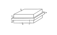
図1に、例えば一つ以上の演算処理装置からなるICを典型的に有する組立電子部品を有する本発明に係る電子装置を示す。 FIG. 1 shows an electronic device according to the present invention having an assembled electronic component typically having an IC consisting of one or more arithmetic processing units, for example.
組立部品1の上面11および下面12のそれぞれは、保護層2によって覆われている。各保護層2は、少なくとも磁気遮蔽層を有し、予め設定された小面積の領域を除いて、前記上面11および下面12の全表面を実質的に覆っている。前記小面積の一部領域には電気接続端子8,9が設けられる。このような予め設定された領域は、好ましくは、前記組立部品1の外周領域1aが含まれてもよく、また前記組立部品1の上面11および下面12の一部領域は保護層が設けられていなくとも良い。
Each of the
図2は、図1と似ているが、上面11のみに保護層2が設けられて保護されているICを示す。
FIG. 2 shows an IC similar to FIG. 1 but protected by providing the
図9は、ICなどの組立電子部品1を有する本発明にかかる電子装置の実施例を示すもので、この実施例では、組立電子部品1がスマートカード内に設けられている。 FIG. 9 shows an embodiment of an electronic apparatus according to the present invention having an assembled electronic component 1 such as an IC. In this embodiment, the assembled electronic component 1 is provided in a smart card.
本発明の他の好適な実施例は、ICなどの組立部品1に図2の保護層2を形成する他の構成を示している図3〜8を参照して説明する。
Another preferred embodiment of the present invention will be described with reference to FIGS. 3 to 8 showing another configuration for forming the
以下の説明は、前記組立部品1の上面11に保護層2を設ける場合についてのものである。しかし、組立部品1の下面12に保護層2を設ける場合も同様な方法により形成することができる。
In the following description, the
図3〜8において、電気接続端子8,9は図示されておらず、図9において示されている。それら端子は、組立部品1の保護層2に覆われていない部分に簡単に設置され、前記保護層2は基本的には遮蔽層20から構成される。
3 to 8, the
前記遮蔽層20は、基本的に、典型的には500を超える高い比透磁率μrを有する軟磁性材料から構成された第1の層21を有する。
The
前記第1の層21は、典型的には、2〜40μm、好ましくは10〜30μmの厚さを有する。
The
図3に示すように、前記第1の層21は、Tiあるいは酸化チタンからなるシード層22の上に成長される。前記シード層22は、典型的には、8〜20nmもしくは100nmの範囲の厚さ、好ましくは10〜15nmの薄い厚さを有する。このシード層22には穴23がパターン形成されていても良い。
As shown in FIG. 3, the
前記パターン形成層22(図4)により同じ穴23を有する軟磁性層21をパターン成長させることができる。
The soft
シード層22と、軟磁性材料から構成された第1の層21とからなるパターン化遮蔽層20は、不均質な磁気信号に調和し、それ故に良好な遮蔽を実現する。
The patterned
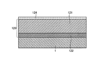
図5および6の実施例は、それぞれ図3および4の実施例と類似しており、符号120、121、122、123で示される要素は、それぞれ符号20、21、22、23に対応しているので、それらの説明を省略する。しかし、図5および6の実施例においては、追加の外層124が、軟磁性材料からなる第1の層121の上に積層されている。この層124は、前記遮蔽層を化学的攻撃から保護する役目を果たすもので、Coベースの化合物などの化学耐性磁気材料から構成される。
The embodiment of FIGS. 5 and 6 is similar to the embodiment of FIGS. 3 and 4, respectively, and elements indicated by
前記追加の外層124は1〜2μmの厚さを有し、機械的研磨や化学的腐食に対して良好な耐性を示す機械的硬質層である。
The additional
前記追加の外層124は、Tiから構成しても良く、SiO2やAl2O3などの非磁性酸化物から構成しても良い。また、この層124はダイヤモンド様カーボンから構成しても良い。
The additional
様々な軟磁性材料を前記第1の層21、121に用いることができる。例えば、パーマロイ組成(Ni80%、Fe20%)に近い組成を有するNiFe合金、CoNi合金、CoZr合金あるいはさらに複雑な系の非常に高い比透磁率μrを有する材料を用いることができる。かかる種類の材料を用いることにより、10000を超える比透磁率μrを得ることができる。
Various soft magnetic materials can be used for the
堆積温度および/または焼鈍温度は、前記ICに適用可能なものに制限されなければならない。具体的には、前記温度の上限は、技術に依存したもので、約350℃である。 The deposition temperature and / or annealing temperature must be limited to those applicable to the IC. Specifically, the upper limit of the temperature is about 350 ° C. depending on the technology.
前記第1の層21、121の厚みは、その他の制約の範囲内で可能な限り厚くすべきである。
The thickness of the
例えば、パーマロイ膜の場合、2〜4dB/μmの減衰が得られる。厚みが10μmの場合、30dBの減衰を実現できる。また、60dBの減衰は、20μmの厚みで実現できる。 For example, in the case of a permalloy film, attenuation of 2 to 4 dB / μm is obtained. When the thickness is 10 μm, an attenuation of 30 dB can be realized. Further, attenuation of 60 dB can be realized with a thickness of 20 μm.
より一般的には、減衰を求める一般式は、前記層の厚みをd、前記RF場の周波数をfとすると、これらの関数として、
a=exp(kd/f)
で与えられる。
前記係数kは材料に依存する。パーマロイの場合では、k=0.5MHzμm-1である。
More generally, the general equation for determining attenuation is as follows: where d is the thickness of the layer and f is the frequency of the RF field,
a = exp (kd / f)
Given in.
The coefficient k depends on the material. In the case of permalloy, k = 0.5 MHz μm −1 .
また、前記遮蔽層20、120は、遮光層として用いても良い。遮光を目的とする場合に選択されるこの層の厚みは、その材料の浸入度に直接相関する。 The shielding layers 20 and 120 may be used as a light shielding layer. The thickness of this layer selected for light shielding purposes is directly correlated to the degree of penetration of the material.
0.1μm〜2μmの範囲の波長光(近紫外光〜赤外光)の光周波数を想定した場合、2μmの良質な金属層により十分に遮光できる。良質な金属層とは、約100μオームcm未満の固有抵抗を有する層である。これには、NiFe、CoZr、Co、NiまたはFeなどのほとんどの金属磁性層が当てはまる。 When an optical frequency of light having a wavelength in the range of 0.1 μm to 2 μm (near ultraviolet light to infrared light) is assumed, it can be sufficiently shielded by a good metal layer of 2 μm. A good metal layer is a layer having a resistivity of less than about 100 μohm cm. This applies to most metal magnetic layers such as NiFe, CoZr, Co, Ni or Fe.
さらに一般的には、500nmを超える厚みでは、その軟磁性層は、近紫外光、可視光および赤外光に対して、その伝導特性から、不透明体となる。したがって、かかる保護層を設けることによって前記チップの光励起を防止することができる。 More generally, when the thickness exceeds 500 nm, the soft magnetic layer becomes an opaque body due to its conduction characteristics with respect to near-ultraviolet light, visible light, and infrared light. Therefore, the photoexcitation of the chip can be prevented by providing such a protective layer.
層21、121の組成の選択は、ウエットエッチング、反応性イオンエッチング(RIE)、イオンビームエッチング(IBE)および集束イオンビーム(FIB)ツールまたはIDS OptiFIB(SCHLUMBERGER社の商標)として知られている集光イオンビームツールなどのICデバッグ用ツールを含む様々な方法によるエッチングの困難性を考慮して行う必要がある。
Selection of the composition of the
Coを含有する層にはウエットエッチングによるエッチングは困難である。Tiを有する層にはRIEあるいはIBEによるエッチングは困難である。 Etching by wet etching is difficult for the layer containing Co. Etching by RIE or IBE is difficult for a layer containing Ti.
また、複合層20、120は、Tiあるいは酸化チタンからなるシード層22、122、パーマロイ層21、121、およびCo合金を主成分とした第2の軟磁性層24、124から構成することができる。
The composite layers 20 and 120 can be composed of seed layers 22 and 122 made of Ti or titanium oxide, permalloy layers 21 and 121, and second soft
前記層の堆積は、電着、プラズマ溶射、スクリーン印刷、スパッタリング、気相堆積(CVD、PECVD、PVD)、液相コーティングあるいは蒸着などの数種の技術によって行うことができる。 The layer can be deposited by several techniques such as electrodeposition, plasma spraying, screen printing, sputtering, vapor deposition (CVD, PECVD, PVD), liquid phase coating or evaporation.
図7および8は、本発明の特殊な実施例を示すもので、この実施例では、遮蔽層20は図3および4の実施例の場合と同様に形成されるが、この遮蔽層20の上には、摂動層31が設けられる。
FIGS. 7 and 8 show a special embodiment of the invention, in which the
前記摂動層31は、組立電子部品1内の電流により生成される磁場よりも大きな磁場を生成することを目的とする。
The
前記摂動層31は不均質な硬質磁性層から構成されても良い。
The
一つの可能な実施例によれば、前記摂動層31は外部に静的な高い磁場を生成する不均質な硬質永久磁性層から構成される。しかし、硬質永久磁性層が均質である場合、外部に生成される磁場は非常に小さいものとなる。
According to one possible embodiment, the
したがって、構造的あるいは磁気的にいくらか不均質とすることにより、印加された磁場に対して免疫を得ることが可能となる。 Therefore, it is possible to obtain immunity against an applied magnetic field by making it somewhat heterogeneous structurally or magnetically.
一つの可能な実施例によれば、前記摂動層31は外部に静的な高い磁場を生成する不均質な硬質永久磁性層から構成される。しかし、硬質永久磁性層が均質である場合、外部に生成される磁場は非常に小さいものとなる。
According to one possible embodiment, the
したがって、構造的あるいは磁気的にいくらか不均質とする。構造的な不均一性の利点は、印加された磁場に対する免疫が得られることである。係る理由から、かかる構成は最も効果的な防護を実現できると考えられる。 Therefore, it is somewhat heterogeneous structurally or magnetically. The advantage of structural heterogeneity is that immunity to the applied magnetic field is obtained. For this reason, such a configuration is considered to provide the most effective protection.
この硬質永久磁性層の組成としては、CoPt、FePt、NdFeB、SmCo5、あるいはFeTb粒子などの他の希土類/遷移金属合金などが可能である。 The composition of this hard permanent magnetic layer can be CoPt, FePt, NdFeB, SmCo 5 , or other rare earth / transition metal alloys such as FeTb particles.
前記摂動層の厚みは、その材質に依存する。厚み1〜5μmの膜は、その膜に垂直な方向に磁化すると、該系の外側にかなり大きな磁場を生成することができる。この厚みは、2kOe(CoPt)〜20kOe(FeNdB)の範囲で変動する材質の残留磁場に相関する。 The thickness of the perturbation layer depends on the material. A film with a thickness of 1-5 μm can generate a fairly large magnetic field outside the system when magnetized in a direction perpendicular to the film. This thickness correlates with the residual magnetic field of the material that varies in the range of 2 kOe (CoPt) to 20 kOe (FeNdB).
前記構造的不均質は、主に3つの異なった方法により実現できる。すなわち、粗い層を用いることによって、層をパターン化することによって、そして、磁性物質と非磁性物質との混合物を用いることによって。 Said structural heterogeneity can be realized mainly in three different ways. That is, by using a coarse layer, by patterning the layer, and by using a mixture of magnetic and non-magnetic materials.
a)前記摂動層31の外表面32を堆積技術によって粗くする(図7)。特に、電着によって非常に粗い表面を形成することができる。また、粗粒により表面32を機械的に研磨することにより、人工的な粗さを実現できる。
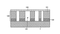
a) The
b)層31をパターニングし、エッチングにより除去部33を形成する方法は、より洗練された方法であり、良好に制御された外部磁場を生成することができる(図8)。5μm以下の寸法にパターン化することにより、摂動層を非常に効果的なものとすることができる。層20および31のパタンニングは、紫外線リソグラフィーを用いて行うことができる。保護領域に依存した特殊な形状を採用することができる。パッド端子用の開口を実装する必要がある。このリソグラフィー工程は、フルサイズのウエハ上にて実行可能である。
b) The method of patterning the
c)また、層31は、非磁性の、絶縁性もしくは導電性の母材中に磁性材料を埋め込んでなる不均質な一組の磁性材料を使用することもできる。この磁性材料は、製造コストを下げるために、接着剤、樹脂、ポリイミド層を含むことができる。
c) The
ポリマーレジストとNdFeB粒子との混合物をスクリーン印刷により堆積する方法は、さらに安価で、簡易な方法である。前記NdFeB粒子はランダムに配向され、それらの保磁力は2テスラを実現する。前記粒子は、ゼロ平均の場が得られることのないように、1μmを超える大きさでなければならない。理想的なサイズは、ランダム分布で1〜20μmの範囲であり、このサイズは機械的粉砕によって得られるサイズである。 A method of depositing a mixture of a polymer resist and NdFeB particles by screen printing is a cheaper and simpler method. The NdFeB particles are randomly oriented and their coercivity is 2 Tesla. The particles must be larger than 1 μm so that a zero average field is not obtained. The ideal size is in the range of 1-20 μm with a random distribution, which is the size obtained by mechanical grinding.
さらに他の実施例によれば、前記摂動層31は揺動磁気層によって構成される。この実施例では、非磁性母剤中に揺動磁性粒子が埋め込まれてなる層が用いられる。
According to another embodiment, the
揺動磁性粒子は、超常磁性形態の粒子である。この形態は、前記粒子のサイズが十分に小さく、粒子の密度が十分に低い(典型的には10%小さく、浸透濃度より明らかに小さい)場合に、実現される。したがって、前記粒子の磁気異方性エネルギーと他の粒子によって生成された磁場のゼーマン・エネルギーが、熱エネルギーkTよりも低くなる。
粒子の典型的なサイズは、直径3〜8nmである。
The oscillating magnetic particles are superparamagnetic particles. This form is realized when the size of the particles is small enough and the density of the particles is low enough (typically 10% smaller and clearly smaller than the osmotic concentration). Accordingly, the magnetic anisotropy energy of the particles and the Zeeman energy of the magnetic field generated by other particles are lower than the thermal energy kT.
The typical size of the particles is 3-8 nm in diameter.
前記サイズを用いることによって、前記IC動作周波数の領域内に揺動周波数を得ることができる。前記粒子のサイズと前記揺動周波数の関係は、f=f0exp(−K1Vμ/kT)によって与えられる。前記式中、K1は異方性定数、Vは粒子の体積、μはユニタリーモーメント、kはボルツマン定数、Tは動作温度、そしてf0は109Hzオーダーの素周波数である。 By using the size, the oscillation frequency can be obtained in the region of the IC operating frequency. The relationship between the particle size and the oscillation frequency is given by f = f 0 exp (−K 1 Vμ / kT). Where K 1 is the anisotropy constant, V is the particle volume, μ is the unitary moment, k is the Boltzmann constant, T is the operating temperature, and f 0 is the elementary frequency on the order of 10 9 Hz.
前記粒子の磁気組成は重要ではない。前記非磁性母材は金属でも絶縁母材でもよい。 The magnetic composition of the particles is not critical. The nonmagnetic base material may be a metal or an insulating base material.
前記粒子の形成は、化学的方法、堆積法のどちらを用いて行っても良い。 The formation of the particles may be performed using either a chemical method or a deposition method.
前記摂動層31は、図5および6の実施例の遮蔽層120の上に形成しても良いし、同様に、図3および4の実施例の遮蔽層20の上に形成しても良い。
The
本発明にかかる遮蔽電子装置は、少なくとも一つの能動組立電子部品1を有するスマートカードに適用し得ることは明らかである。この場合、本発明にかかる遮蔽電子装置は、前記上面11と下面12の少なくとも一つ(11)と、前記組立電子部品1によって放射される電磁(EM)および/または高周波(RF)電界に対抗する少なくとも一つの遮蔽層2(この層は前出の図の遮蔽層20、120と同じもの)とを有し、前記遮蔽層2が500を超える大きさの高い非透磁率μrを有する軟磁性材料からなる少なくとも一つの第1の層21または121を有し、前記遮蔽層2が、前記上面11および下面12の少なくとも一つ(11)の、外部装置と接続する電気接続端子を設けるための予め設定された領域1a、23,123を除いたほぼ全表面上に設けられている。
It is obvious that the shielding electronic device according to the present invention can be applied to a smart card having at least one active assembly electronic component 1. In this case, the shielding electronic device according to the present invention resists at least one of the
図9に示した好適な実施例では、本発明にかかる遮蔽電子装置は、上面11および下面12の両方を有するとともに、前記組立電子部品1によって放射される電磁(EM)および/または高周波(RF)電界に対抗する、前出の図の遮蔽層20または120と同じ少なくとも一つの遮蔽層2を有し、前記遮蔽層2が500を超える大きさの高い非透磁率μrを有する軟磁性材料からなる少なくとも一つの第1の層21または121を有し、前記遮蔽層2が、前記上面11および下面12の両方の表面の、外部装置と接続する電気接続端子8,9を設けるための予め設定された領域1a、23,123を除いたほぼ全表面上に設けられている。
In the preferred embodiment shown in FIG. 9, the shielding electronic device according to the present invention has both an
電気接続端子8,9は、前記組立電子部品1の上面11の周縁部分1aに設けられても良い。
The
遮蔽層2は、前記組立電子部品1の上面11および下面12の周縁部分1aを除いた全表面に設けられても良い。
The
前記組立電子部品1は、例えば、演算処理装置やメモリーから構成される。この組立電子部品1は、その2つの遮蔽層2とともに、エポキシ基板5の上に接着剤層4により組み付けられている。
The assembly electronic component 1 includes, for example, an arithmetic processing unit and a memory. The assembled electronic component 1 is assembled together with its two
前記組立部品1の電気接続端子8,9は、金線などの配線81,91を介して、前記エポキシ基板5の下面に設けられているパッド6,7に接続されている。前記配線81、91は前記基板5に形成された穴51,52を通って前記接続パッド6,7に、例えば、NiCu/金端子を介して、接続されている。
The
前記エポキシ基板5は、プラスチックカード本体101に埋め込まれている。前記プラスチック本体101には、盲穴が形成されており、この盲穴は、少なくとも前記電子部品1、遮蔽層2、配線81,91、およびエポキシ基板5を収納可能な深さに形成されている。このプラスチック本体101には、窪んだ平面53,54が形成されている。この窪んだ平面53,54の形状は環状でも矩形でも良く、その深さは前記エポキシ基板5の厚みに依存している。すなわち、前記接続パッド6,7の外表面がプラスチックカード本体101の下面とほぼ同一平面をなすように、窪んだ平面53,54の深さが設定されている。前記プラスチック本体101には、一般的に、印刷パターン、文字あるいは図画が施されている。前記エポキシ基板5は一般に前記窪んだ平面53,54に接着されている。
The epoxy substrate 5 is embedded in the
本発明の他の目的は、保護すべき組立電子部品を有する遮蔽電子装置の製造方法を提供することにある。この遮蔽電子装置は、上面11および下面12を有するとともに、外部交信のための電気接続端子を有しており、この遮蔽電子装置の製造方法は、上面11および下面12の少なくとも一つ(11)の上に、前記組立電子部品1によって放射される電磁(EM)および/または高周波(RF)電界に対抗する、前出の図の遮蔽層20または120と同じ少なくとも一つの遮蔽層2を形成する工程と、500を超える大きさの高い非透磁率μrを有する軟磁性材料からなる少なくとも一つの第1の層21または121を有する前記遮蔽層2を、前記上面11および下面12の少なくとも一つ(11)の表面の、外部装置と接続する電気接続端子8,9を設けるための予め設定された領域1a、23,123を除いたほぼ全表面上に、設ける工程を有する。
Another object of the present invention is to provide a method of manufacturing a shielded electronic device having an assembled electronic component to be protected. The shielded electronic device has an
好ましくは、本発明にかかる製造方法は、少なくとも一つの遮蔽層2を形成する前記工程において、
a)電気接続端子8,9を有する上面11および下面12の少なくとも一つ(11)の上にシード層22,122を形成するために、機械的硬質層をスパッタリング技術によって堆積する工程、および
b)電着によって、高い比透磁率を有する軟磁性材料からなる層21,121を形成する工程を有する。
Preferably, the manufacturing method according to the present invention includes the step of forming at least one
a) depositing a mechanical hard layer by sputtering technique to form the seed layers 22, 122 on at least one of the
好ましくは、本発明にかかる製造方法は、少なくとも一つの遮蔽層2を形成する前記工程において、前記遮蔽層2をパターンニングして除去部分23,123を形成し、それにより、前記電気接続端子8,9を設けるための限られた面積の前記予め設定した領域1a、23,123のいくつかを構成する工程であって、前記軟磁性材料からなる層21,121を電着により堆積する前に、前記シード層22,122をパターン化する工程を、さらに有する。
Preferably, in the manufacturing method according to the present invention, in the step of forming at least one
好ましくは、本発明にかかる製造方法は、少なくとも一つの遮蔽層2を形成する前記工程において、最上面に追加の機械的硬質層124を形成する工程を、さらに有する。
Preferably, the manufacturing method according to the present invention further includes a step of forming an additional mechanical
好ましくは、本発明にかかる製造方法は、前記遮蔽層2上に、前記組立電子部品1から放出される電磁(EM)および高周波(RF)電界と少なくとも同等の大きさの強い磁気摂動を誘導し得る不均質硬質磁気材料からなる摂動層31を形成する工程を、さらに有する。
Preferably, the manufacturing method according to the present invention induces a strong magnetic perturbation on the
好ましくは、本発明にかかる製造方法は、前記摂動層31を形成する工程において、非磁性母材中に揺動磁性粒子を組み入れる工程を有する。
Preferably, the manufacturing method according to the present invention includes a step of incorporating oscillating magnetic particles in the nonmagnetic base material in the step of forming the
以下に本発明の具体的実施例を示す。 Specific examples of the present invention are shown below.
(実施例1)
遮蔽層120を、三層:10nmのTi(層122);20μmのNiFe(層121);および1μmのCoZr(層124)から構成する。その厚みは、変更可能であるが、合計厚さは、20〜40μmであることが、好ましい。
Example 1
The
摂動層31として、NdFeBからなる硬質磁性層をスクリーン印刷により堆積させる。
As the
1)10nmのTiシード層122をスパッタリングにより堆積させる。この層は室温にて堆積させる。堆積速度は、ターゲット/試料間の距離が8cm、200Wで、約2
m/秒である。そして、レジストマスクを積層し、シード層を領域123が形成される特定の形状にエッチングする。他の方法として、レジストマスクを形成した後、前記Tiシード層122を堆積し、リフトオフ法を使用してもよい。
1) A 10 nm
m / sec. Then, a resist mask is stacked, and the seed layer is etched into a specific shape in which the
2)第2の工程として、前記Tiシード層122の上に、電着により、20μm厚のNiFe層121を成長させる。NiFeの具体的堆積速度は1μm/分である。NiFe溶液の温度と濃度を均一とすることにより、かなり扁平なNiFe層を形成することができる。
2) As a second step, a 20 μm
3)次に、CoZr最外層124を電着により堆積させる。
3) Next, the CoZr
4)摂動層31を、1〜20μmのNdFeB粒子を組み込んだポリイミド樹脂から形成する。この摂動層31は1μmを超える厚みとする必要がある。
4) The
(実施例2)
遮蔽層120を、三層:10nmのTi(層122);20μmのNiFe(層121);および1μmのCoZr(層124)から構成する。その厚みは、変更可能であるが、合計厚さは、20〜40μmであることが、好ましい。
(Example 2)
The
摂動層31はCoPtP合金の硬質磁性層から形成する。
The
1)10nmのTiシード層122をスパッタリングにより堆積させる。この層122は室温にて堆積させる。堆積速度は、ターゲット/試料間の距離が8cm、200Wで、約2nm/秒である。そして、レジストマスクを積層し、シード層を領域123が形成される特定の形状にエッチングする。他の方法として、レジストマスクを形成した後、前記Tiシード層122を堆積し、リフトオフ法を使用してもよい。
1) A 10 nm
2)第2の工程として、前記Tiシード層122の上に、電着により、20μm厚のNiFe層121を成長させる。NiFeの具体的堆積速度は1μm/分である。NiFe溶液の温度と濃度を均一とすることにより、かなり扁平なNiFe層を形成することができる。
2) As a second step, a 20 μm
3)次に、CoZr最外層124を電着により堆積させる。
3) Next, the CoZr
4)CoPt層31は電着法により成長させることができる。この層の成長は、最大の摂動を生成するように算定した所定のパターン形状のレジストマスクを介して実施することができる。この場合、かかる材料の保磁力を0.15テスラとすることができる。表面に生成される漂遊磁界は10mT(105A/m)のオーダーとなる。
4) The
(実施例3)
遮蔽層120を、三層:10nmのTi(層122);20μmのNiFe(層121);および1μmのCoZr(層124)から構成する。その厚みは、変更可能であるが、合計厚さは、20〜40μmであることが、好ましい。
(Example 3)
The
摂動層31は揺動Co粒子から形成する。
The
1)10nmのTiシード層122をスパッタリングにより堆積させる。この層122は室温にて堆積させる。堆積速度は、ターゲット/試料間の距離が8cm、200Wで、約2nm/秒である。そして、レジストマスクを積層し、シード層を領域123が形成される特定の形状にエッチングする。他の方法として、レジストマスクを形成した後、前記Tiシード層122を堆積し、リフトオフ法を使用してもよい。
1) A 10 nm
2)第2の工程として、前記Tiシード層122の上に、電着により、20μm厚のNiFe層121を成長させる。NiFeの具体的堆積速度は1μm/分である。NiFe溶液の温度と濃度を均一とすることにより、かなり扁平なNiFe層を形成することができる。
2) As a second step, a 20 μm
3)次に、CoZr最外層124を電着により堆積させる。
3) Next, the CoZr
4)摂動層31を、Co粒子をAg、Al2O3またはSiO中に組み込んだ材料から、摂動層31を形成する。かかる系は、例えば同時スパッタリングによりかなり容易に製造することができ、非常に耐壊性が高いという2つの利点を得ることができる。好適なCo濃度、約10%は、Co源をスパッタする電力を低減することにより、得ることができる。Co/Ag系は、これら2つの元素は混和しないので、特に容易に製造することができる。したがって、室温での堆積により、非常に小さな粒子が得られる。250℃超400℃未満の温度での焼鈍によって、サイズを増大させることができる。携帯製品のRF放出を覆う良好なサイズである約3〜5nmの揺動粒子を得るには、250℃1時間の焼鈍で十分である。
4) The
以上のように、本発明にかかる遮蔽電子装置は、保護すべき電子組立部品を有し、扁平な携帯用製品に組み込まれる電子装置の無線高周波の放出を不正な者が検出することを防ぐことができる。また、本発明の遮蔽電子装置は、電子装置の能動部品が光および赤外線によって改ざんされることから電子装置を保護することができる。さらに、本発明の遮蔽電子装置は、化学的腐食またはイオン腐食による剥離に対する高い機械耐性を有する As described above, the shielded electronic device according to the present invention has electronic assembly parts to be protected, and prevents unauthorized persons from detecting the radio high frequency emission of the electronic device incorporated in a flat portable product. Can do. Further, the shielded electronic device of the present invention can protect the electronic device from the active parts of the electronic device being tampered with by light and infrared rays. Furthermore, the shielded electronic device of the present invention has a high mechanical resistance against peeling due to chemical or ionic corrosion.
1 組立電子部品
1a 組立電子部品の周縁部分
1a,23,123 電気接続端子を設けるための予め設定された領域
8,9 外部交信用の電気接続端子
11 組立電子部品の上面
12 組立電子部品の下面
20,120 遮蔽層
21,121 第1の層
22,122 シード層
31 摂動層
124 追加の外層
DESCRIPTION OF SYMBOLS 1 Assembly
Claims (31)
前記上面(11)と下面(12)の少なくとも一つ(11)と、前記組立電子部品(1)から放出する電磁(EM)および/または高周波(RF)電界に対抗する少なくとも一つの遮蔽層(20、120)とを有し、前記遮蔽層(20,120)が500を超える大きさの高い非透磁率μrを有する軟磁性材料からなる少なくとも一つの第1の層(21、121)を有し、前記遮蔽層(120)が機械的研磨や化学的腐食に良好な耐性を示す機械的硬質層である追加の外層(124)をさらに有し、前記遮蔽層(20,120)が、前記上面(11)および下面(12)の少なくとも一つ(11)の、外部装置と接続する前記電気接続端子を設けるための予め設定された領域(1a、23,123)を除いたほぼ全表面上に設けられていることを特徴とする遮蔽電子装置。 A shielded electronic device having at least one assembled electronic component (1) to be protected and having an upper surface (11), a lower surface (12), and an electrical connection terminal (8, 9) for external communication,
At least one of the upper surface (11) and the lower surface (12) (11) and at least one shielding layer against electromagnetic (EM) and / or radio frequency (RF) fields emitted from the assembled electronic component (1). 20, 120) and having at least one first layer wherein the shielding layer (20, 120) is made of soft magnetic material with a high relative magnetic permeability mu r larger than 500 (the 21, 121) The shielding layer (120) further comprises an additional outer layer (124) that is a mechanical hard layer exhibiting good resistance to mechanical polishing and chemical corrosion, the shielding layer (20, 120) comprising: At least one surface (11) of at least one of the upper surface (11) and the lower surface (12) except for a preset region (1a, 23, 123) for providing the electrical connection terminal connected to an external device. Provided above A shielding electronic device characterized by the above.
前記上面(11)および下面(12)の少なくとも一つ(11)の上に、前記組立電子部品(1)から放出される電磁(EM)および/または高周波(RF)電界に対抗する、少なくとも一つの遮蔽層(20,120)を形成する工程と、500を超える大きさの高い非透磁率μrを有する軟磁性材料からなる少なくとも一つの第1の層(21,121)を有する前記遮蔽層(20,120)を、前記上面(11)および下面(12)の少なくとも一つ(11)の表面の、前記電気接続端子(8,9)を設けるための予め設定された領域(1a、23,123)を除いたほぼ全表面上に、設ける工程を有することを特徴とする遮蔽電子装置の製造方法。 A method of manufacturing a shielded electronic device having at least one assembled electronic component (1) to be protected, having an upper surface (11) and a lower surface (12), and having an electrical connection terminal for external communication,
On at least one (11) of the upper surface (11) and the lower surface (12), at least one against an electromagnetic (EM) and / or radio frequency (RF) electric field emitted from the assembly electronic component (1). forming one of the shielding layer (20, 120), said shielding layer having at least one first layer made of soft magnetic material with a size of high relative permeability mu r exceeding 500 (21, 121) (20, 120) on a surface of at least one of the upper surface (11) and the lower surface (12) (11), a predetermined region (1a, 23) for providing the electrical connection terminals (8, 9) , 123), and a method of manufacturing a shielding electronic device, comprising a step of providing on substantially the entire surface.
a)電気接続端子(8,9)を有する上面(11)および下面(12)の少なくとも一つ(11)の上にシード層(22,122)を形成するために、機械的硬質層をスパッタリング技術によって堆積する工程、および
b)電着によって、高い比透磁率を有する軟磁性材料からなる層(21,121)を形成する工程を有することを特徴とする請求項26に記載の方法。 Said step of forming at least one shielding layer (20, 120);
a) Sputtering a mechanical hard layer to form a seed layer (22, 122) on at least one (11) of the upper surface (11) and the lower surface (12) having electrical connection terminals (8, 9) 27. A method according to claim 26, comprising the step of depositing by technique, and b) forming a layer (21, 121) of soft magnetic material having a high relative permeability by electrodeposition.
Applications Claiming Priority (2)
| Application Number | Priority Date | Filing Date | Title |
|---|---|---|---|
| EP04291122A EP1594163A1 (en) | 2004-05-03 | 2004-05-03 | A screened electrical device and a process for manufacturing the same |
| PCT/EP2005/004636 WO2005106953A1 (en) | 2004-05-03 | 2005-04-27 | A screened electrical device and a process for manufacturing the same |
Publications (1)
| Publication Number | Publication Date |
|---|---|
| JP2007536752A true JP2007536752A (en) | 2007-12-13 |
Family
ID=34931065
Family Applications (1)
| Application Number | Title | Priority Date | Filing Date |
|---|---|---|---|
| JP2007511981A Pending JP2007536752A (en) | 2004-05-03 | 2005-04-27 | Shielding electronic device and manufacturing method thereof |
Country Status (9)
| Country | Link |
|---|---|
| US (1) | US8415774B2 (en) |
| EP (2) | EP1594163A1 (en) |
| JP (1) | JP2007536752A (en) |
| KR (1) | KR20070055419A (en) |
| CN (1) | CN1977380A (en) |
| AT (1) | ATE373875T1 (en) |
| DE (1) | DE602005002558T2 (en) |
| ES (1) | ES2293569T3 (en) |
| WO (1) | WO2005106953A1 (en) |
Cited By (1)
| Publication number | Priority date | Publication date | Assignee | Title |
|---|---|---|---|---|
| JP2007043090A (en) * | 2005-08-01 | 2007-02-15 | Samsung Electronics Co Ltd | Semiconductor package with ferrite shielding texture |
Families Citing this family (16)
| Publication number | Priority date | Publication date | Assignee | Title |
|---|---|---|---|---|
| CN101373741B (en) * | 2007-08-21 | 2010-06-23 | 海华科技股份有限公司 | Semiconductor shielding structure and manufacturing method thereof |
| US8733652B2 (en) | 2010-11-18 | 2014-05-27 | Nagravision S.A. | Method and apparatus for communicating between a security module and a host device |
| EP2455887B1 (en) | 2010-11-18 | 2016-08-24 | Nagravision S.A. | Method and apparatus for communicating between a security module and a host device |
| EP2455886A1 (en) | 2010-11-18 | 2012-05-23 | Nagravision S.A. | Interface between a security module and a host device |
| US9055665B2 (en) | 2010-11-18 | 2015-06-09 | Nagravision S.A.S | Interface between a security module and a host device |
| CA2912594A1 (en) | 2013-05-16 | 2015-02-19 | National Institute Of Aerospace Associates | Radiation hardened microelectronic chip packaging technology |
| EP2997595B1 (en) * | 2013-05-16 | 2020-11-18 | National Institute Of Aerospace Associates | Method of forming a radiation hardened microelectronic chip package |
| FR3027705B1 (en) * | 2014-10-27 | 2017-12-22 | Oberthur Technologies | MICROCIRCUIT MODULE, METHOD FOR MANUFACTURING MICROCIRCUIT MODULE, ELECTRONIC DEVICE COMPRISING SUCH A MODULE |
| US11211340B2 (en) | 2018-11-28 | 2021-12-28 | Shiann-Tsong Tsai | Semiconductor package with in-package compartmental shielding and active electro-magnetic compatibility shielding |
| US10896880B2 (en) | 2018-11-28 | 2021-01-19 | Shiann-Tsong Tsai | Semiconductor package with in-package compartmental shielding and fabrication method thereof |
| US10923435B2 (en) | 2018-11-28 | 2021-02-16 | Shiann-Tsong Tsai | Semiconductor package with in-package compartmental shielding and improved heat-dissipation performance |
| TWI744572B (en) | 2018-11-28 | 2021-11-01 | 蔡憲聰 | Semiconductor package with in-package compartmental shielding and fabrication method thereof |
| US11239179B2 (en) | 2018-11-28 | 2022-02-01 | Shiann-Tsong Tsai | Semiconductor package and fabrication method thereof |
| US10718880B2 (en) * | 2018-11-29 | 2020-07-21 | Schlumberger Technology Corporation | High-voltage protection and shielding within downhole tools |
| TWI728604B (en) * | 2019-01-01 | 2021-05-21 | 蔡憲聰 | Semiconductor package with in-package compartmental shielding and active electro-magnetic compatibility shielding |
| FR3111737B1 (en) * | 2020-06-19 | 2022-07-08 | Commissariat Energie Atomique | CHIP OR BOX-SYSTEM PROTECTION USING THE GMI EFFECT |
Citations (4)
| Publication number | Priority date | Publication date | Assignee | Title |
|---|---|---|---|---|
| JPH04174543A (en) * | 1990-07-20 | 1992-06-22 | Seiko Epson Corp | Semiconductor device |
| JPH05275554A (en) * | 1992-03-25 | 1993-10-22 | Sumitomo Special Metals Co Ltd | Semiconductor device |
| JPH08204054A (en) * | 1995-01-23 | 1996-08-09 | Tokin Corp | Electronic device |
| JP2003347441A (en) * | 2002-05-22 | 2003-12-05 | Sharp Corp | Semiconductor element, semiconductor device, and method for producing semiconductor element |
Family Cites Families (12)
| Publication number | Priority date | Publication date | Assignee | Title |
|---|---|---|---|---|
| JPH0744110B2 (en) | 1988-09-02 | 1995-05-15 | 松下電器産業株式会社 | High saturation magnetic flux density soft magnetic film and magnetic head |
| US5138431A (en) | 1990-01-31 | 1992-08-11 | Vlsi Technology, Inc. | Lead and socket structures with reduced self-inductance |
| CA2092371C (en) * | 1993-03-24 | 1999-06-29 | Boris L. Livshits | Integrated circuit packaging |
| US5294826A (en) * | 1993-04-16 | 1994-03-15 | Northern Telecom Limited | Integrated circuit package and assembly thereof for thermal and EMI management |
| JP2970590B2 (en) * | 1997-05-14 | 1999-11-02 | 日本電気株式会社 | Magnetoresistive element, magnetoresistive sensor using the same, magnetoresistive detection system and magnetic storage system |
| US6121544A (en) * | 1998-01-15 | 2000-09-19 | Petsinger; Julie Ann | Electromagnetic shield to prevent surreptitious access to contactless smartcards |
| US6515352B1 (en) * | 2000-09-25 | 2003-02-04 | Micron Technology, Inc. | Shielding arrangement to protect a circuit from stray magnetic fields |
| JP2003124538A (en) * | 2001-10-16 | 2003-04-25 | Sony Corp | Information storage device and electronic equipment mounted with the same information storage device |
| JP3907461B2 (en) * | 2001-12-03 | 2007-04-18 | シャープ株式会社 | Manufacturing method of semiconductor module |
| US6767592B2 (en) * | 2001-12-05 | 2004-07-27 | Seagate Technology Llc | Method for thin film protective overcoat |
| US6906396B2 (en) * | 2002-01-15 | 2005-06-14 | Micron Technology, Inc. | Magnetic shield for integrated circuit packaging |
| JP4013140B2 (en) * | 2003-01-15 | 2007-11-28 | ソニー株式会社 | Magnetic memory device |
-
2004
- 2004-05-03 EP EP04291122A patent/EP1594163A1/en not_active Withdrawn
-
2005
- 2005-04-27 EP EP05736562A patent/EP1745509B1/en active Active
- 2005-04-27 JP JP2007511981A patent/JP2007536752A/en active Pending
- 2005-04-27 CN CNA2005800220513A patent/CN1977380A/en active Pending
- 2005-04-27 KR KR1020067025541A patent/KR20070055419A/en not_active Application Discontinuation
- 2005-04-27 WO PCT/EP2005/004636 patent/WO2005106953A1/en active Application Filing
- 2005-04-27 AT AT05736562T patent/ATE373875T1/en not_active IP Right Cessation
- 2005-04-27 DE DE602005002558T patent/DE602005002558T2/en active Active
- 2005-04-27 ES ES05736562T patent/ES2293569T3/en active Active
- 2005-04-27 US US11/579,365 patent/US8415774B2/en active Active
Patent Citations (4)
| Publication number | Priority date | Publication date | Assignee | Title |
|---|---|---|---|---|
| JPH04174543A (en) * | 1990-07-20 | 1992-06-22 | Seiko Epson Corp | Semiconductor device |
| JPH05275554A (en) * | 1992-03-25 | 1993-10-22 | Sumitomo Special Metals Co Ltd | Semiconductor device |
| JPH08204054A (en) * | 1995-01-23 | 1996-08-09 | Tokin Corp | Electronic device |
| JP2003347441A (en) * | 2002-05-22 | 2003-12-05 | Sharp Corp | Semiconductor element, semiconductor device, and method for producing semiconductor element |
Cited By (1)
| Publication number | Priority date | Publication date | Assignee | Title |
|---|---|---|---|---|
| JP2007043090A (en) * | 2005-08-01 | 2007-02-15 | Samsung Electronics Co Ltd | Semiconductor package with ferrite shielding texture |
Also Published As
| Publication number | Publication date |
|---|---|
| US8415774B2 (en) | 2013-04-09 |
| DE602005002558T2 (en) | 2008-06-26 |
| ES2293569T3 (en) | 2008-03-16 |
| KR20070055419A (en) | 2007-05-30 |
| EP1745509A1 (en) | 2007-01-24 |
| ATE373875T1 (en) | 2007-10-15 |
| US20110068441A1 (en) | 2011-03-24 |
| EP1745509B1 (en) | 2007-09-19 |
| CN1977380A (en) | 2007-06-06 |
| WO2005106953A1 (en) | 2005-11-10 |
| EP1594163A1 (en) | 2005-11-09 |
| DE602005002558D1 (en) | 2007-10-31 |
Similar Documents
| Publication | Publication Date | Title |
|---|---|---|
| JP2007536752A (en) | Shielding electronic device and manufacturing method thereof | |
| KR101020388B1 (en) | Magnetic shielding for electronic circuits which include magnetic materials | |
| US7656630B2 (en) | Active protection device for protecting circuit against mechanical and electromagnetic attack | |
| US4992776A (en) | Antipilferage tags and their use | |
| JP2008249406A (en) | Magnetic impedance effect element and its manufacturing method | |
| KR100801789B1 (en) | Electronic label | |
| JP2008135446A (en) | Method of producing rf powder | |
| JPWO2003009403A1 (en) | Magnetic sensor and method of manufacturing the same | |
| US7053854B2 (en) | Device for shielding a transponder, method for producing a corresponding shielding and transponder provided with said shielding | |
| US7728702B2 (en) | Shielding of integrated circuit package with high-permeability magnetic material | |
| TWI498887B (en) | A read sensor,a method of manufacturing a read sensor,and a read element | |
| JP2004213196A (en) | Semiconductor module, non-contact ic tag and manufacturing method for semiconductor module | |
| US11574652B2 (en) | Recording device and recording method | |
| JPH03129897A (en) | Composite electromagnetic shielding material | |
| CN101395616A (en) | Arrangement comprising an object made at least partially of metal or precious metal and an RFID identification device | |
| RU2386174C2 (en) | Method of protecting from forgery and checking authenticity of valuable articles | |
| JP3806803B2 (en) | Fraud detection sensor using radio waves or magnets for gaming machines | |
| US20150355035A1 (en) | In-package temperature sensor and methods therefor | |
| JPH0546943A (en) | Thin film magnetic head | |
| JP2002043647A (en) | Magnetic impedance effect element | |
| JP2001284698A (en) | Light emitting element | |
| JP2000323700A (en) | Composite device provided with magnetized film layer and its manufacture | |
| JPS61294624A (en) | Magnetoresistance effect type thin film head |
Legal Events
| Date | Code | Title | Description |
|---|---|---|---|
| A621 | Written request for application examination |
Free format text: JAPANESE INTERMEDIATE CODE: A621 Effective date: 20080402 |
|
| A131 | Notification of reasons for refusal |
Free format text: JAPANESE INTERMEDIATE CODE: A131 Effective date: 20100803 |
|
| A601 | Written request for extension of time |
Free format text: JAPANESE INTERMEDIATE CODE: A601 Effective date: 20101102 |
|
| A602 | Written permission of extension of time |
Free format text: JAPANESE INTERMEDIATE CODE: A602 Effective date: 20101110 |
|
| A601 | Written request for extension of time |
Free format text: JAPANESE INTERMEDIATE CODE: A601 Effective date: 20101203 |
|
| A602 | Written permission of extension of time |
Free format text: JAPANESE INTERMEDIATE CODE: A602 Effective date: 20101210 |
|
| A601 | Written request for extension of time |
Free format text: JAPANESE INTERMEDIATE CODE: A601 Effective date: 20101228 |
|
| A602 | Written permission of extension of time |
Free format text: JAPANESE INTERMEDIATE CODE: A602 Effective date: 20110111 |
|
| A521 | Request for written amendment filed |
Free format text: JAPANESE INTERMEDIATE CODE: A523 Effective date: 20110201 |
|
| A02 | Decision of refusal |
Free format text: JAPANESE INTERMEDIATE CODE: A02 Effective date: 20110823 |