JP2007518878A - Support object and method for coating a cutting tool - Google Patents
Support object and method for coating a cutting tool Download PDFInfo
- Publication number
- JP2007518878A JP2007518878A JP2006546895A JP2006546895A JP2007518878A JP 2007518878 A JP2007518878 A JP 2007518878A JP 2006546895 A JP2006546895 A JP 2006546895A JP 2006546895 A JP2006546895 A JP 2006546895A JP 2007518878 A JP2007518878 A JP 2007518878A
- Authority
- JP
- Japan
- Prior art keywords
- support
- support object
- coating
- group
- cutting tool
- Prior art date
- Legal status (The legal status is an assumption and is not a legal conclusion. Google has not performed a legal analysis and makes no representation as to the accuracy of the status listed.)
- Pending
Links
Images


Classifications
-
- C—CHEMISTRY; METALLURGY
- C23—COATING METALLIC MATERIAL; COATING MATERIAL WITH METALLIC MATERIAL; CHEMICAL SURFACE TREATMENT; DIFFUSION TREATMENT OF METALLIC MATERIAL; COATING BY VACUUM EVAPORATION, BY SPUTTERING, BY ION IMPLANTATION OR BY CHEMICAL VAPOUR DEPOSITION, IN GENERAL; INHIBITING CORROSION OF METALLIC MATERIAL OR INCRUSTATION IN GENERAL
- C23C—COATING METALLIC MATERIAL; COATING MATERIAL WITH METALLIC MATERIAL; SURFACE TREATMENT OF METALLIC MATERIAL BY DIFFUSION INTO THE SURFACE, BY CHEMICAL CONVERSION OR SUBSTITUTION; COATING BY VACUUM EVAPORATION, BY SPUTTERING, BY ION IMPLANTATION OR BY CHEMICAL VAPOUR DEPOSITION, IN GENERAL
- C23C16/00—Chemical coating by decomposition of gaseous compounds, without leaving reaction products of surface material in the coating, i.e. chemical vapour deposition [CVD] processes
- C23C16/44—Chemical coating by decomposition of gaseous compounds, without leaving reaction products of surface material in the coating, i.e. chemical vapour deposition [CVD] processes characterised by the method of coating
- C23C16/458—Chemical coating by decomposition of gaseous compounds, without leaving reaction products of surface material in the coating, i.e. chemical vapour deposition [CVD] processes characterised by the method of coating characterised by the method used for supporting substrates in the reaction chamber
- C23C16/4581—Chemical coating by decomposition of gaseous compounds, without leaving reaction products of surface material in the coating, i.e. chemical vapour deposition [CVD] processes characterised by the method of coating characterised by the method used for supporting substrates in the reaction chamber characterised by material of construction or surface finish of the means for supporting the substrate
-
- C—CHEMISTRY; METALLURGY
- C23—COATING METALLIC MATERIAL; COATING MATERIAL WITH METALLIC MATERIAL; CHEMICAL SURFACE TREATMENT; DIFFUSION TREATMENT OF METALLIC MATERIAL; COATING BY VACUUM EVAPORATION, BY SPUTTERING, BY ION IMPLANTATION OR BY CHEMICAL VAPOUR DEPOSITION, IN GENERAL; INHIBITING CORROSION OF METALLIC MATERIAL OR INCRUSTATION IN GENERAL
- C23C—COATING METALLIC MATERIAL; COATING MATERIAL WITH METALLIC MATERIAL; SURFACE TREATMENT OF METALLIC MATERIAL BY DIFFUSION INTO THE SURFACE, BY CHEMICAL CONVERSION OR SUBSTITUTION; COATING BY VACUUM EVAPORATION, BY SPUTTERING, BY ION IMPLANTATION OR BY CHEMICAL VAPOUR DEPOSITION, IN GENERAL
- C23C16/00—Chemical coating by decomposition of gaseous compounds, without leaving reaction products of surface material in the coating, i.e. chemical vapour deposition [CVD] processes
Landscapes
- Chemical & Material Sciences (AREA)
- General Chemical & Material Sciences (AREA)
- Chemical Kinetics & Catalysis (AREA)
- Engineering & Computer Science (AREA)
- Materials Engineering (AREA)
- Mechanical Engineering (AREA)
- Metallurgy (AREA)
- Organic Chemistry (AREA)
- Chemical Vapour Deposition (AREA)
- Cutting Tools, Boring Holders, And Turrets (AREA)
Abstract
本発明は、切屑除去用の切削工具を被覆するための支持物体及びその方法に関する。支持物体は、CVD及び/またはMTCVD法において切削工具インサートを被覆する際に使用するのに適している。この支持物体は、少なくとも支持物体の表面及び/または前記表面下の層がMAX相の群Mn+1AXn(n=1、2、3)から選択された材料から少なくとも部分的になり、Mが周期律表のIIIB、IVB、VB、VIB及びVIII族から選択された1種または2種以上の元素及び/または前記元素の混合物の少なくとも1種であり、Aが周期律表のIIIA、IVA、VA及びVIA族から選択された1種または2種以上の元素及び/または前記元素の混合物の少なくとも1種であり、且つXが炭素及び/または窒素である。The present invention relates to a support and a method for coating a cutting tool for chip removal. The support object is suitable for use in coating cutting tool inserts in CVD and / or MTCVD processes. The support body is at least partly composed of a material in which at least the surface of the support body and / or the layer below the surface is selected from the group M n + 1 AX n (n = 1, 2, 3) of the MAX phase. One or more elements selected from groups IIIB, IVB, VB, VIB and VIII of the periodic table and / or a mixture of said elements, and A is IIIA, IVA, One or more elements selected from the group VA and VIA and / or a mixture of said elements, and X is carbon and / or nitrogen.
Description
本発明は、支持物体と、付加された独立請求項の前段にしたがう切屑除去用の切削工具(割り出し可能な切削インサート)を被覆するためのその被覆方法に関する。 The present invention relates to a supporting object and its coating method for coating a cutting tool for chip removal (indexable cutting insert) according to the preceding paragraph of the appended independent claim.
CVD(化学蒸着)で堆積した耐摩耗層、具体的には超硬合金切削インサート上のTiC、Ti(C、N)、TiN及びAl2O3が、30年の間工業的に製造されてきた。CVD及び/またはMTCVD(中温化学蒸着)の層の堆積条件に係わる詳細、及びCVD及び/またはMTCVDを基にする層の設計が、文献並びに特許において広範囲に検討されてきている。 Wear resistant layers deposited by CVD (chemical vapor deposition), specifically TiC, Ti (C, N), TiN and Al 2 O 3 on cemented carbide cutting inserts have been industrially produced for 30 years. It was. Details concerning the deposition conditions of CVD and / or MTCVD (medium temperature chemical vapor deposition) layers and the design of layers based on CVD and / or MTCVD have been extensively studied in the literature and patents.
CVD及び/またはMYCVD技術の主要な利点の一つは、同一バッチ処理において非常に沢山の工具の被覆が可能であり、インサートの大きさ及び使用する装置に依存して30,000個におよび、切削インサート全周に被膜を備えた安い製造価格のインサートを提供する。均一な被膜厚み分布を得るために、切削インサートの機能表面が、被覆作業の際、比較的等しく分離されていることが重要である。しかしながら、被覆作業の際に、工具が被覆されるだけでなく、切削インサートを載せる支持部は、インサートがこの支持部の表面とともに成長するような結果と成る。被覆サイクルの終了後にインサートが取除かれたときに、接触マークがこれらの場所に現れる。 One of the main advantages of CVD and / or MYCVD technology is that it allows for very many tool coatings in the same batch process, up to 30,000 depending on the size of the insert and the equipment used. A low-priced insert with a coating around the cutting insert. In order to obtain a uniform coating thickness distribution, it is important that the functional surfaces of the cutting insert are relatively equally separated during the coating operation. However, during the coating operation, not only the tool is coated, but also the support on which the cutting insert is placed results in the insert growing with the surface of this support. Contact marks appear at these locations when the insert is removed after the end of the coating cycle.
これらの接触マークは体裁的な問題だけでない。このマークが金属切削作業の際の作業中に実際に表面に現れた場合、このマークが工具寿命の減少をもたらすであろう。さらに、インサートの支持表面は、切削インサートの工具ホルダーへの誤った位置決めを回避するために、膨らんだマークのない平坦にする必要がある。誤って位置決めされた切削インサートは、切削工具の性能にマイナスの影響をもたらす。即ち、靭性が減少し、加工部品の精度と表面仕上げが劣る。接触マークのマイナスの影響を最小にするために、幾つかの完全な配置が報告されており、これは機能面から他の区域にこのマークを移動することを目的とする。 These contact marks are not just a cosmetic problem. If this mark actually appears on the surface during a metal cutting operation, this mark will result in reduced tool life. Furthermore, the support surface of the insert needs to be flat without bulging marks in order to avoid incorrect positioning of the cutting insert into the tool holder. Incorrectly positioned cutting inserts have a negative impact on cutting tool performance. That is, the toughness is reduced and the precision and surface finish of the machined parts are poor. In order to minimize the negative effects of the contact mark, several complete arrangements have been reported, which are aimed at moving this mark from the functional area to other areas.
CVD及び/またはMTCVDで被覆したインサートのバッチ処理装てん方法の他の重要な態様は、切削インサートの形状の相違のために、非常に順応性を必要とする。典型的な標準CVD及びMTCVDの被膜は、内接円が5mmから50mmまで変化する種々の大きさの切削インサートに堆積される。切削インサートの基本形は非常に変化し、例えば、長方形、八角形、四角形、円形、三角形、ダイアモンド形などである。切削インサートは、中央の穴を備えるか備えないで、2mmから10mmまで変化する種々の厚みを有する。一つの典型的なCVD及び/またはMTCVDの被覆サイクルは、したがって、種々の配置を必要とする切削インサート全ての数百に相当する種々の形状に堆積する。したがって、均一装てん密度を得るために、種々の切削インサート形状に対して種々の配置を必然的に必要とするバッチ処理を装備する方法は、低価格及び短い準備時間に焦点を絞った製造環境では決して合理的に作動することができない。 Another important aspect of the batch loading method of inserts coated with CVD and / or MTCVD is very adaptable due to the difference in the shape of the cutting insert. Typical standard CVD and MTCVD coatings are deposited on cutting inserts of various sizes with inscribed circles varying from 5 mm to 50 mm. The basic shape of the cutting insert varies greatly, for example, rectangular, octagonal, quadrangular, circular, triangular, diamond-shaped, etc. Cutting inserts have various thicknesses varying from 2 mm to 10 mm with or without a central hole. One typical CVD and / or MTCVD coating cycle thus deposits in a variety of shapes, representing hundreds of all cutting inserts that require a variety of arrangements. Therefore, in order to obtain a uniform loading density, the method of equipping batch processing, which necessarily requires different arrangements for different cutting insert geometries, is in a manufacturing environment focused on low cost and short preparation times. It can never operate reasonably.
欧州特許第454,686号は、特にPACVDを目的とした装備する方法を開示し、切削インサートは、中間スペーサのあるなしに係わらず中央ピンの互いの頂部に積み重ねられる。この方法をCVD及び/またはMTCVDに使用することは、種々の切削インサートは種々のピンの構成を必要とするので、第1に、上述するように普遍的な方法でないので、種々の不利益が生じるであろう。第2に切削インサートに穴を必要とする。第3に、厚いCVD及び/またはMTCVDの層を付ける場合、互いに成長する傾向が強まる積層された切削インサートからの圧力のため、切削インサートはスペーサ及び/または他の切削インサートに非常に強く付着するであろう。 EP 454,686 discloses a mounting method specifically intended for PACVD, in which cutting inserts are stacked on top of each other of the central pin with or without an intermediate spacer. Using this method for CVD and / or MTCVD has various disadvantages because, first, various cutting inserts require various pin configurations, and thus are not universal methods as described above. Will occur. Second, it requires holes in the cutting insert. Third, when applying thick CVD and / or MTCVD layers, the cutting inserts adhere very strongly to spacers and / or other cutting inserts due to pressure from stacked cutting inserts that tend to grow together. Will.
米国特許第5,576,058号は、足部、肩部、首部及び頭部を含む種々の掛け釘配置を基にするバッチ処理装備方法を開示する。 US Pat. No. 5,576,058 discloses a batch processing equipment method based on various peg arrangements including feet, shoulders, neck and head.
普通に使用される装備配置は、切削インサートを受け皿の穴または溝に配置することである。この方法は、切れ刃または切削インサートの逃げ面に接触マークが付く。この方法は、切削インサートがその位置から落下することを回避するために、運搬及び受け皿への装備の際に非常に注意深い取扱いを必要とする。また、この配置は、自動切削インサートの装着法が使用される場合、切削インサートは非常に不安定な位置に配置しなければならないので、使用することが非常に難しい。 A commonly used equipment arrangement is to place the cutting insert in a hole or groove in the pan. This method places a contact mark on the flank of the cutting edge or cutting insert. This method requires very careful handling during transportation and mounting of the pan to avoid the cutting insert falling from its position. This arrangement is also very difficult to use because the cutting insert must be placed in a very unstable position when the automatic cutting insert mounting method is used.
さらに別の方法において、切削インサートは棒にネジ止めされる。この棒は、上述と同じ危険を備える欧州特許第454,686号のように垂直に配置されか、または水平に配置される。水平配置のおもな欠点は、全ての形状の切削インサートを処理するために、必然的に種々の取り付けが必要となるので、種々の切削インサート形状に対して普遍性の不足である。さらに、この方法は、穴を備えるインサートだけに使用される。 In yet another method, the cutting insert is screwed to the bar. The bars are arranged vertically or horizontally as in EP 454,686, which carries the same danger as described above. The main disadvantage of the horizontal arrangement is the lack of universality for the various cutting insert shapes, since various mountings are necessarily required to process all shapes of cutting inserts. Furthermore, this method is only used for inserts with holes.
最も普遍的な配置は、金網またはその他の表面(ほとんどはグラファイトで作られる)の必要なスペース表面に切削インサートを簡単に配置することを基本にしている。このバッチ処理は、この金網をスペーサによって互いに分離されている頂部に固定することによって、またはこの金網が固定されるグラファイト運搬具を用いることによって、積み重なり合う。この処理の最大の欠点は、今までのところ金網と切削インサートの間に形成される接触マークがほとんど存在する。これらのマークは、工具ホルダーへの切削インサートの不正確な位置だしとなり、且つ切削インサートの深刻な性能低下となるであろう。ほとんどが形成されたこれらのマークを除去するために、研削加工のようなある種の後処理を必要とする。この金網についての別の不都合は、切削インサートが堆積される前に比較的容易に互いに滑りあうことができるので、それによって切削インサート上に被覆されていない区域が現れる。 The most universal arrangement is based on a simple arrangement of the cutting insert on the required space surface of a wire mesh or other surface (mostly made of graphite). The batch process is stacked by securing the wire mesh to the tops separated from each other by spacers, or by using a graphite carrier to which the wire mesh is secured. The biggest drawback of this process is that so far there is almost a contact mark formed between the wire mesh and the cutting insert. These marks will lead to inaccurate positioning of the cutting insert in the tool holder and will result in severe performance degradation of the cutting insert. Some post-processing such as grinding is required to remove most of these formed marks. Another disadvantage with this wire mesh is that it can slide relative to each other relatively easily before the cutting inserts are deposited, thereby revealing uncovered areas on the cutting inserts.
本発明の目的は、被覆の際切削インサートに接触マークを形成することを回避する支持物体を提供することである。
本発明の別の目的は、被覆の際切削インサートに積み重なりあいの形成を回避する支持物体を提供することである。
本発明の別の目的は、被覆の際切削インサートに積み重なりあいの形成を回避する方法を提供することである。
本発明の目的は、従属項の特徴とする部分に定義される特徴を備える方法及び支持物体によって実現される。
It is an object of the present invention to provide a support object that avoids forming contact marks on the cutting insert during coating.
Another object of the present invention is to provide a support object that avoids the formation of stacking on the cutting insert during coating.
Another object of the present invention is to provide a method that avoids the formation of stacking on the cutting insert during coating.
The object of the present invention is realized by a method and a support body with the features defined in the characterizing part of the dependent claims.
続いての記載において、我々は次のような事項を使用する。
事前被膜は、網または支持材料上で添付するCVO及び/またはMTCVDの層を定義し、且つ、製造被膜は、ここで定義される最終製品状の耐摩耗性のCVD及び/またはMTCVDの層の堆積に以前に被覆される。
In the description that follows, we will use the following:
The pre-coating defines the CVO and / or MTCVD layer attached on the mesh or support material, and the production coating is the end product like wear-resistant CVD and / or MTCVD layer as defined herein. Previously deposited on deposition.
ここに使用される「MAX相の群」は、材料がMn+1AXn(n=1,2,3)を含むことを意味し、Mは、周期律表のIIIB、IVB、VB、VIB及びVIII族から選択された1種または2種以上の金属及び/または前記金属の混合物の少なくとも1種であり、Aが、周期律表のIIIA、IVA、VA及びVIA族から選択された1種または2種以上の金属及び/または前記金属の混合物の少なくとも1種であり、且つ
Xが、炭素及び/または窒素である。
As used herein, “group of MAX phases” means that the material includes M n + 1 AX n (n = 1, 2, 3), where M is IIIB, IVB, VB, VIB and One or more metals selected from group VIII and / or a mixture of said metals, wherein A is one selected from groups IIIA, IVA, VA and VIA of the periodic table or It is at least one of two or more metals and / or a mixture of said metals, and X is carbon and / or nitrogen.
Ti3SiC2は、MAX相の群のひとつの材料であり、且つその注目すべき特性は既知である。その特性は、容易な機械加工性、硬さ、熱衝撃耐性、耐損傷性、強靭性、高温強度、耐酸化性及び耐食性である。いままではそれはTi金属密度を有していた。この材料は、電気ヒータ用(国際出願第WO02/51208号)、溶融金属用(米国特許出願第2003075251号)、及び切削インサートの被膜用(スウェーデン特許第0202036−0号)のような幾つかの適用が考慮されている。 Ti 3 SiC 2 is one material in the group of MAX phases and its remarkable properties are known. Its properties are easy machinability, hardness, thermal shock resistance, damage resistance, toughness, high temperature strength, oxidation resistance and corrosion resistance. As it was, it had a Ti metal density. This material is available in several applications, such as for electric heaters (International Application No. WO02 / 51208), for molten metals (U.S. Patent Application No. 2003075251), and for coating of cutting inserts (Swedish Patent No. 0202036-0). Application is considered.
本発明にしたがって、インサートと直接または間接に接触している表面及び/または支持物体が、MAX相の群から選択された材料を実質的に含む場合、大きな接触マーク、特に突出しているマークを回避可能である驚くべきことが判明した。基本的に切削インサートと接触している支持物体(例えばポリアミドの円錐状など)の性質は、先行技術の問題を抑制できる。 In accordance with the present invention, large contact marks, particularly protruding marks, are avoided if the surface and / or support object that is in direct or indirect contact with the insert substantially comprises a material selected from the group of MAX phases. It turned out to be surprising that is possible. The nature of the support body (eg, the polyamide cone) that is essentially in contact with the cutting insert can suppress the problems of the prior art.
本発明にしたがい、切削インサートと直接または間接に接触して使用される材料は、上記で定義したようなMAX相の材料を実質的に含み、好ましくは85wt%以上を含んで成る。 In accordance with the present invention, the material used in direct or indirect contact with the cutting insert substantially comprises a MAX phase material as defined above, and preferably comprises 85 wt% or more.
一つの実施態様において、一つ以上のMは、周期律表のIVB、VB及びVIB族から選択される。
一つの実施態様において、一つ以上のAはSi、Al、GaまたはGeである。
別の実施態様において、MAX相は、Mn+1AXnにおいてn=2のタイプである。
さらに別の好ましい実施態様においては、MAX相は、実質的にTi3SiC2好ましくは少なくとも85wt%を含み、残部は、TiC、TiSi2、Ti5Si3またはSiCの1種以上である。
In one embodiment, one or more M is selected from groups IVB, VB and VIB of the periodic table.
In one embodiment, one or more of A is Si, Al, Ga or Ge.
In another embodiment, the MAX phase is of type n = 2 in M n + 1 AX n .
In yet another preferred embodiment, the MAX phase substantially comprises Ti 3 SiC 2, preferably at least 85 wt%, with the balance being one or more of TiC, TiSi 2 , Ti 5 Si 3 or SiC.
この材料は、例えば米国特許第5,942,455号に記載するように先行技術において既知である。 This material is known in the prior art, for example as described in US Pat. No. 5,942,455.
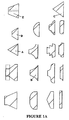
この支持物体は、図1A及び図1Bに示す実際の切削インサート形状に適するために、A、B、C、D及びEが双方の図に示される形状を表現する種々の幾何学形状に形成することができる。それぞれの支持物体は、図示しないが、支持する物体に接触する基部または主表面を有する。一般的には切削インサートは支持物体上に載せられ、切削インサートの穴に向かって突き出ている支持物体の部分を備える。実施例の点線は、被覆される両側側面を示す切削インサートを表現する。ほとんどの場合には、切削インサートを支持物体に重力保持されることに注目すべきである。中央穴を備えた切削インサートに対しては、その形状は3個以上の側面を備える角錐状、または円錐状のように好ましく作られる。この角錐形の円錐形は、また10μm〜2mmの半径と置き換えることができる。また、半径のあるまたは半径を備えないこの角錐形は、凹状及び/または凸状の中間側面区分を含んで製造することができる。可能な限り切削インサート形状に依存せずに普遍的な形状を保障するために、角錐形または円錐形の露出側面が、真っ直ぐであるか、或いは唯一つの半径例えば凹面がトランペット状または凸面が弾丸状のように形成することが好ましい。 In order to be suitable for the actual cutting insert shape shown in FIGS. 1A and 1B, this support object is formed into various geometric shapes where A, B, C, D and E represent the shapes shown in both figures. be able to. Although not shown, each supporting object has a base or main surface that contacts the supporting object. In general, the cutting insert rests on a support object and comprises a part of the support object protruding towards the hole in the cutting insert. The dotted lines in the examples represent cutting inserts showing the side surfaces to be coated. It should be noted that in most cases the cutting insert is gravity held by the support body. For a cutting insert with a central hole, the shape is preferably made like a pyramid with three or more sides, or a cone. This pyramidal cone can also be replaced with a radius of 10 μm to 2 mm. Also, this pyramidal shape with or without a radius can be manufactured including concave and / or convex intermediate side sections. The pyramid or conical exposed side is straight, or only one radius, for example concave is trumpet or convex is bullet-like, to ensure universal shape as much as possible regardless of cutting insert shape It is preferable to form as follows.
角錐形または円錐形は、さらに容易にそれらの取り扱いをするために、幾分切り詰めることができる。また、切り詰められた角錐形または円錐形は、次の支持物体用の支持として使用することができる。 The pyramids or cones can be somewhat truncated to make them easier to handle. Also, the truncated pyramid or conical shape can be used as a support for the next support object.
さらに、切り詰められた角錐形または円錐形は、ガス流形態を改良するために、中央の穴で作ることもできる。また、角錐形または円錐形の望ましい表面粗さは、利点を提供する。 Furthermore, truncated pyramids or cones can be made with a central hole to improve gas flow morphology. Also, the desired surface roughness of a pyramid or cone provides an advantage.
単一側面を持った切削インサート、すなわち、インサートの底側は作業に使用されないインサートに対して、切削インサートは、MAX相の群から選ばれた材料の支持物体上に直接位置決めすることができる。これは、この側面が重要でない効果であり機能的でないので、支持物体に向き合う切削インサートの側面上にさらに薄い層を備える。その後、この表面は穴の有無に関らず、平坦な表面或いは凸凹のある表面を形成することができる。この凸凹のある表面は、高さと平滑な寸法で規則的または不規則に変化する極小形態として形成することができる。図2Aは、被覆作業の際に、単一側面を備える切削インサートの支持物体に使用できる表面形態を有する本発明の六つの支持物体の実施例を示す。図2Bは他の実施例を斜視図で示し、単一側面を備えた切削インサート用の本発明にしたがう支持物体一部分を示す。この図2Bは、巨視的または微視的な形状の双方を存在させることができる。 For cutting inserts with a single side, i.e. inserts where the bottom side of the insert is not used for work, the cutting insert can be positioned directly on a support of material selected from the group of MAX phases. This is provided with a thinner layer on the side of the cutting insert facing the support object, since this side is an insignificant effect and not functional. Thereafter, this surface can form a flat surface or an uneven surface with or without holes. This uneven surface can be formed as a minimal feature that changes regularly or irregularly in height and smooth dimensions. FIG. 2A shows an example of six support objects of the present invention having a surface morphology that can be used for a support object of a cutting insert with a single side during a coating operation. FIG. 2B shows another embodiment in perspective view, showing a portion of a support object according to the present invention for a cutting insert with a single side. This FIG. 2B can have both a macroscopic or microscopic shape.
好ましい規則的かつ微視的な形態は、50μm〜5mmの基部と20μm〜5mmの高さとを備える三つ以上の側面を有する角錐形とすることができる。50μm〜500μmのRa値を備える微細な表面粗さを得るためのブラスト加工、ブラシ加工またはスクラチ加工の方法が、不規則な形態を得ることができる。 A preferred regular and microscopic form may be a pyramid with three or more sides with a base of 50 μm to 5 mm and a height of 20 μm to 5 mm. Blasting, brushing, or scrambling methods for obtaining fine surface roughness with Ra values of 50 μm to 500 μm can obtain irregular forms.
好ましい実施態様においては、支持物体は、最初の製造被膜の使用前に、周期律表のIVB、VB及びVIB族からの金属の窒化物及び/または炭化物及び/または酸化物の5〜100μmの厚みの被膜で事前被覆される。 In a preferred embodiment, the support body is 5-100 μm thick of metal nitrides and / or carbides and / or oxides from groups IVB, VB and VIB of the periodic table prior to use of the first production coating. Pre-coated with a coating of
より厚い製造被膜の切削インサートを支持するために支持物体としての使用する際、より厚い被膜がこの支持物体の頂部に堆積される。驚くことには、このことはその結果にマイナスに影響を及ぼさないことが判明した。支持材料としての本発明にしたがう支持物体の寿命は、好ましい特性のいずれの劣化もなく、50回の製造被膜の回数より多い。 When used as a support body to support a thicker production coating cutting insert, a thicker film is deposited on top of the support body. Surprisingly, this has been found to have no negative effect on the results. The lifetime of a support body according to the invention as a support material is greater than 50 production coatings without any degradation of the preferred properties.
切削インサートは、MAX相の群から選ばれた材料で作られた本発明にしたがう支持物体上に位置決めするために支持される。 The cutting insert is supported for positioning on a support object according to the present invention made of a material selected from the group of MAX phases.
本発明は切削インサートを参照して記載したが、他の形の被覆構成物例えばエンドミル、摩耗部品などの処理に使用可能であることは明確である。 Although the invention has been described with reference to cutting inserts, it is clear that it can be used to process other forms of coating components such as end mills, wear parts, and the like.
被覆する際に切削工具インサートが配置されることを意図している支持物体の少なくとも区域は、MAX相の群から選ばれた材料から成る。MAX相の群の材料から実質的に全体が成る支持物体に代えて、支持物体の少なくとも表面及び/またはこの表面の真下の層が、MAX相の群から選ばれた材料から少なくとも部分的に成ることが考えられる。例えば、任意の材料の支持物体が、MAX相の群から選ばれた材料の少なくとも一つの表面層で被覆される。この表面層は、工具インサートの被覆の際の接触マークを回避するために十分な厚みにする必要がある。この支持物体の表面層の厚みは、少なくとも25μmの厚みにする。 At least the area of the support body on which the cutting tool insert is intended to be placed when coating is made of a material selected from the group of MAX phases. Instead of a support body consisting essentially of the material of the MAX phase group, at least the surface of the support object and / or the layer directly below this surface consists at least partly of a material selected from the group of MAX phases. It is possible. For example, a support body of any material is coated with at least one surface layer of material selected from the group of MAX phases. This surface layer needs to be thick enough to avoid contact marks when coating the tool insert. The thickness of the surface layer of the supporting body is at least 25 μm.
実施例1
真っ直ぐな隅部を備える4つの側面を備える角錐形、すなわち、図1A及び図2Bに示す10mmの側面と高さ7mmの基部を備える改良型Aは、少量の不純物を含むMAX相の材料Ti3SiC2から作られ、以後改良型A−MAXと称呼し、かつグラファイトの改良型A−グラファイトと称呼する。この角錐形は、直径3mmの規則的に配置された穴を有する平坦なグラファイト受け皿状に配置される。この角錐形は、25μmの合計厚みのTi(C、N)+Al2O3+TiNのCVD及びMTCVDの層で事前被覆される。P25適用のための型式CNMG120408の超硬合金切削インサートが、二つの改良型の全ての角錐形上に位置付けされた。改良型当たり全部で100個の角錐形が使用された。
Example 1
The pyramid shape with four sides with straight corners, ie the modified A with 10 mm sides and 7 mm height base shown in FIGS. 1A and 2B, is a MAX phase material Ti 3 with a small amount of impurities. Made of SiC 2 and hereinafter referred to as modified A-MAX and referred to as graphite modified A-graphite. This pyramid is arranged in a flat graphite pan with regularly arranged holes of 3 mm diameter. This pyramid is pre-coated with CVD and MTCVD layers of Ti (C, N) + Al 2 O 3 + TiN with a total thickness of 25 μm. A cemented carbide cutting insert of type CNMG120408 for P25 application was positioned on all two pyramid shapes. A total of 100 pyramids per modification were used.
約15μmの合計被膜厚みを備えるTi(C、N)+Al2O3+TiNのCVD/MTCVDの製造被膜が、切削インサートに堆積された。 Ti (C, N) + Al 2 O 3 + TiN CVD / MTCVD production coating with a total coating thickness of about 15 μm was deposited on the cutting insert.
被覆後に、全ての切削インサートは、ステレオ顕微鏡でマークを10倍の倍率で検査した。このマークは、目視不可、20μm高さより小さい目視可能マーク、20μm高さ以上のマークについて分類した。20μm高さの臨界大きさは、この製品に良好な性能を与えることができる最大の大きさであるために選ばれた。
測定された切削インサートは、事前被覆した後に、最初の製造被膜の工程で被覆された。以下の表1はその結果を要約する。
After coating, all cutting inserts were inspected with a stereo microscope at 10x magnification. This mark was classified into a visually invisible mark, a visible mark smaller than 20 μm height, and a mark of 20 μm height or more. A critical size of 20 μm height was chosen because it is the largest size that can give good performance to this product.
The measured cutting inserts were coated in the first production coating step after precoating. Table 1 below summarizes the results.
表1
目視可能マーク 20μm以下の 20μm以上の 付着
の無いインサー 目視可能マーク 目視可能マーク 程度
トの数 を有するインサ を有するインサ
ートの数 ートの数
改良型 73 27 0 なし
A−MAX
(本発明)
改良型 0 62 28 付着
グラファイト
(従来例) Table 1
Visible mark 20 μm or less Adhered to 20 μm or more
Inserter without mark Visible mark Visible mark Degree
Insa with the number of
Number of books
Improved 73 27 0 None A-MAX
(Invention)
Improved 0 62 28 Adhering graphite
(Conventional example)
改良型A−MAXは、同一の支持物体の形状を備えるのにもかかわらず、A−グラファイトより少なくかつ小さなマークであることが明確である。また、A−MAXの角錐形は付着が無い。この試験は、MAX相の群から選ばれた材料の支持物体の利点を示す。 It is clear that the improved A-MAX is fewer and smaller marks than A-graphite, despite having the same support object shape. The A-MAX pyramid has no adhesion. This test shows the advantage of a support of material selected from the group of MAX phases.
実施例2
91wt%のWC−9wt%のCoの組成を有しXOMX0908−ME06形状の単一の側面を備える超硬合金切削インサートが用いられた。堆積前に、被覆されていない下地は洗浄された。約5μmの合計被膜厚みを有するTi(C、N)+Al2O3+TiNのCVD製造被膜が切削インサートに堆積された。
Example 2
A cemented carbide cutting insert with a single side of XOMX0908-ME06 shape with a composition of 91 wt% WC-9 wt% Co was used. Prior to deposition, the uncoated substrate was cleaned. A CVD manufactured film of Ti (C, N) + Al 2 O 3 + TiN having a total film thickness of about 5 μm was deposited on the cutting insert.
この切削インサートは、図1Aのものと同じで軽量であるが大きい平らな受け皿の上で直接堆積された。この受け皿は、改良型A−MAXで少量の不純物を含む実質的にTi3SiC2を含んで成るグラファイトの支持物体、及び改良型A−グラファイトから成る。この領域の厚みは5mmであった。この領域は、製造被膜の検査前に、CVD及びMTCVDのTi(C、N)+Al2O3+TiNの被膜で20μmの合計被膜厚みに事前被覆された。全部で100個のインサートが被覆された。 This cutting insert was deposited directly on the same flat, lightweight but large flat saucer as in FIG. 1A. The saucer consists of a modified A-MAX, a graphite support substantially comprising Ti 3 SiC 2 containing a small amount of impurities, and an improved A-graphite. The thickness of this region was 5 mm. This region was pre-coated with a CVD and MTCVD Ti (C, N) + Al 2 O 3 + TiN coating to a total coating thickness of 20 μm prior to inspection of the production coating. A total of 100 inserts were coated.
被膜製造後に、全部の切削インサートが、実施例1にしたがって検査された。
測定された切削インサートは、事前被覆した後、最初の製造被覆工程において被覆された。表2はその結果の要約である。
After cutting the coating, all cutting inserts were inspected according to Example 1.
The measured cutting inserts were pre-coated and then coated in the first production coating process. Table 2 summarizes the results.
表2
目視可能マーク 20μm以下の 20μm以上の 付着
の無いインサー 目視可能マーク 目視可能マーク 程度
トの数 を有するインサ を有するインサ
ートの数 ートの数
改良型 88 12 0 なし
A−MAX
(本発明)
改良型 0 77 23 付着
グラファイト
(従来例) Table 2
Visible mark 20 μm or less Adhered to 20 μm or more
Inserter without mark Visible mark Visible mark Degree
Insa with the number of
Number of books
Improved type 88 12 0 None A-MAX
(Invention)
Improved 0 77 23 Adhering graphite
(Conventional example)
本発明の改良型A−MAXは、最良の結果を明確に示し、大部分の切削インサートはいずれのマークもなく完全であり、マークの付いたものはそのマークが20μmより小さかった。また、この実施例において、付着の明確な相違を検出することができた。 The improved A-MAX of the present invention clearly showed the best results, most cutting inserts were complete without any marks, and those with marks were smaller than 20 μm. In this example, a clear difference in adhesion could be detected.
本発明は、論理的かつ生産的な状態でかつ硬質かつ耐摩耗性の耐火性層を備えた大きな容積の切削インサート被覆するための方法及び支持物体に関する。この方法は、被覆過程に使用する耐久性のある支持材料として、MAX相の群から選ばれた材料の使用を基にする。この方法において、従来の方法の欠点すなわち接触マークを減少させることを可能であることが判明した。 The present invention relates to a method and a support for coating large volumes of cutting inserts in a logical and productive state and with a hard and wear-resistant refractory layer. This method is based on the use of a material selected from the group of MAX phases as a durable support material for use in the coating process. It has been found that in this method it is possible to reduce the disadvantages of the conventional method, ie the contact marks.
Claims (10)
前記支持物体の少なくとも表面及び/または前記表面の下の層が、MAX相の群であるMn+1AXn(n=1、2、3)から選択された材料から少なくとも部分的になり、
Mが、元素周期律表のIIIB、IVB、VB、VIB及びVIII族から選択された金属及び/または前記金属の混合物の少なくとも1種であり、
Aが、元素周期律表のIIIA、IVA、VA及びVIA族から選択された金属及び/または前記金属の混合物の少なくとも1種であり、且つXが、炭素及び/または窒素である、
ことを特徴とする支持物体。 A support object suitable for supporting one or more cutting tool inserts during coating of the cutting tool inserts in CVD and / or MTCVD processes,
At least a surface of the support and / or a layer below the surface is at least partially made of a material selected from M n + 1 AX n (n = 1, 2, 3) which is a group of MAX phases;
M is at least one metal selected from groups IIIB, IVB, VB, VIB and VIII of the Periodic Table of Elements and / or a mixture of said metals;
A is at least one metal selected from groups IIIA, IVA, VA and VIA of the Periodic Table of Elements and / or a mixture of said metals, and X is carbon and / or nitrogen.
A support object characterized by that.
下地、及びCVD及び/またはMTCVD法を用いて堆積した被膜より成る切削工具インサートを被覆する方法。 The cutting insert is coated with a substrate, characterized in that it is positioned on a support object as defined in claim 1, and a cutting tool insert comprising a coating deposited using CVD and / or MTCVD methods. Method.
Applications Claiming Priority (2)
| Application Number | Priority Date | Filing Date | Title |
|---|---|---|---|
| SE0303595A SE526833C2 (en) | 2003-12-19 | 2003-12-22 | Support for coating tool using CVD or MTCVD comprises MAX material to avoid contact mark formation |
| PCT/SE2004/001857 WO2005061759A1 (en) | 2003-12-22 | 2004-12-13 | Carrier body and method for coating cutting tools. |
Publications (2)
| Publication Number | Publication Date |
|---|---|
| JP2007518878A true JP2007518878A (en) | 2007-07-12 |
| JP2007518878A5 JP2007518878A5 (en) | 2007-12-20 |
Family
ID=34676091
Family Applications (1)
| Application Number | Title | Priority Date | Filing Date |
|---|---|---|---|
| JP2006546895A Pending JP2007518878A (en) | 2003-12-22 | 2004-12-13 | Support object and method for coating a cutting tool |
Country Status (7)
| Country | Link |
|---|---|
| US (1) | US20050132957A1 (en) |
| EP (1) | EP1709214A1 (en) |
| JP (1) | JP2007518878A (en) |
| KR (1) | KR20060123381A (en) |
| CN (1) | CN1898412A (en) |
| CZ (1) | CZ2006399A3 (en) |
| WO (1) | WO2005061759A1 (en) |
Cited By (1)
| Publication number | Priority date | Publication date | Assignee | Title |
|---|---|---|---|---|
| WO2015182552A1 (en) * | 2014-05-28 | 2015-12-03 | 京セラ株式会社 | Cutting insert manufacturing method |
Families Citing this family (299)
| Publication number | Priority date | Publication date | Assignee | Title |
|---|---|---|---|---|
| SE527351C2 (en) * | 2003-07-10 | 2006-02-14 | Seco Tools Ab | Method of coating inserts |
| US8347811B2 (en) * | 2006-10-05 | 2013-01-08 | Michael Bucci | System and method for supporting an object during application of surface coating |
| SE531749C2 (en) | 2007-09-17 | 2009-07-28 | Seco Tools Ab | Method of precipitating durable layers on cemented carbide with arc evaporation and cathode with Ti3SiC2 as the main component |
| US10378106B2 (en) | 2008-11-14 | 2019-08-13 | Asm Ip Holding B.V. | Method of forming insulation film by modified PEALD |
| US9394608B2 (en) | 2009-04-06 | 2016-07-19 | Asm America, Inc. | Semiconductor processing reactor and components thereof |
| CN101550545B (en) * | 2009-04-30 | 2012-07-25 | 深圳市金洲精工科技股份有限公司 | Device for inserting and placing shank for precision cutter diamond coating, and processing equipment |
| US8802201B2 (en) | 2009-08-14 | 2014-08-12 | Asm America, Inc. | Systems and methods for thin-film deposition of metal oxides using excited nitrogen-oxygen species |
| US9023493B2 (en) * | 2010-07-13 | 2015-05-05 | L. Pierre de Rochemont | Chemically complex ablative max-phase material and method of manufacture |
| US9312155B2 (en) | 2011-06-06 | 2016-04-12 | Asm Japan K.K. | High-throughput semiconductor-processing apparatus equipped with multiple dual-chamber modules |
| US10364496B2 (en) | 2011-06-27 | 2019-07-30 | Asm Ip Holding B.V. | Dual section module having shared and unshared mass flow controllers |
| US10854498B2 (en) * | 2011-07-15 | 2020-12-01 | Asm Ip Holding B.V. | Wafer-supporting device and method for producing same |
| US20130023129A1 (en) | 2011-07-20 | 2013-01-24 | Asm America, Inc. | Pressure transmitter for a semiconductor processing environment |
| US9017481B1 (en) | 2011-10-28 | 2015-04-28 | Asm America, Inc. | Process feed management for semiconductor substrate processing |
| CN102534565B (en) * | 2012-03-22 | 2013-07-03 | 株洲欧科亿硬质合金有限公司 | Load boat for production of coating knife and application thereof |
| US9659799B2 (en) | 2012-08-28 | 2017-05-23 | Asm Ip Holding B.V. | Systems and methods for dynamic semiconductor process scheduling |
| US9021985B2 (en) | 2012-09-12 | 2015-05-05 | Asm Ip Holdings B.V. | Process gas management for an inductively-coupled plasma deposition reactor |
| US10714315B2 (en) | 2012-10-12 | 2020-07-14 | Asm Ip Holdings B.V. | Semiconductor reaction chamber showerhead |
| US20160376700A1 (en) | 2013-02-01 | 2016-12-29 | Asm Ip Holding B.V. | System for treatment of deposition reactor |
| US9589770B2 (en) | 2013-03-08 | 2017-03-07 | Asm Ip Holding B.V. | Method and systems for in-situ formation of intermediate reactive species |
| US9484191B2 (en) | 2013-03-08 | 2016-11-01 | Asm Ip Holding B.V. | Pulsed remote plasma method and system |
| US9240412B2 (en) | 2013-09-27 | 2016-01-19 | Asm Ip Holding B.V. | Semiconductor structure and device and methods of forming same using selective epitaxial process |
| CN103726031A (en) * | 2013-12-24 | 2014-04-16 | 成都工具研究所有限公司 | Workpiece clamping tool of chemical vapor deposition equipment |
| US10683571B2 (en) | 2014-02-25 | 2020-06-16 | Asm Ip Holding B.V. | Gas supply manifold and method of supplying gases to chamber using same |
| US10167557B2 (en) | 2014-03-18 | 2019-01-01 | Asm Ip Holding B.V. | Gas distribution system, reactor including the system, and methods of using the same |
| US11015245B2 (en) | 2014-03-19 | 2021-05-25 | Asm Ip Holding B.V. | Gas-phase reactor and system having exhaust plenum and components thereof |
| US10858737B2 (en) | 2014-07-28 | 2020-12-08 | Asm Ip Holding B.V. | Showerhead assembly and components thereof |
| US9890456B2 (en) | 2014-08-21 | 2018-02-13 | Asm Ip Holding B.V. | Method and system for in situ formation of gas-phase compounds |
| US10941490B2 (en) | 2014-10-07 | 2021-03-09 | Asm Ip Holding B.V. | Multiple temperature range susceptor, assembly, reactor and system including the susceptor, and methods of using the same |
| US9657845B2 (en) | 2014-10-07 | 2017-05-23 | Asm Ip Holding B.V. | Variable conductance gas distribution apparatus and method |
| KR102263121B1 (en) | 2014-12-22 | 2021-06-09 | 에이에스엠 아이피 홀딩 비.브이. | Semiconductor device and manufacuring method thereof |
| US10529542B2 (en) | 2015-03-11 | 2020-01-07 | Asm Ip Holdings B.V. | Cross-flow reactor and method |
| US10276355B2 (en) | 2015-03-12 | 2019-04-30 | Asm Ip Holding B.V. | Multi-zone reactor, system including the reactor, and method of using the same |
| US10458018B2 (en) | 2015-06-26 | 2019-10-29 | Asm Ip Holding B.V. | Structures including metal carbide material, devices including the structures, and methods of forming same |
| US10600673B2 (en) | 2015-07-07 | 2020-03-24 | Asm Ip Holding B.V. | Magnetic susceptor to baseplate seal |
| US10083836B2 (en) | 2015-07-24 | 2018-09-25 | Asm Ip Holding B.V. | Formation of boron-doped titanium metal films with high work function |
| US9960072B2 (en) | 2015-09-29 | 2018-05-01 | Asm Ip Holding B.V. | Variable adjustment for precise matching of multiple chamber cavity housings |
| US10211308B2 (en) | 2015-10-21 | 2019-02-19 | Asm Ip Holding B.V. | NbMC layers |
| US10322384B2 (en) | 2015-11-09 | 2019-06-18 | Asm Ip Holding B.V. | Counter flow mixer for process chamber |
| US11139308B2 (en) | 2015-12-29 | 2021-10-05 | Asm Ip Holding B.V. | Atomic layer deposition of III-V compounds to form V-NAND devices |
| US10529554B2 (en) | 2016-02-19 | 2020-01-07 | Asm Ip Holding B.V. | Method for forming silicon nitride film selectively on sidewalls or flat surfaces of trenches |
| US10468251B2 (en) | 2016-02-19 | 2019-11-05 | Asm Ip Holding B.V. | Method for forming spacers using silicon nitride film for spacer-defined multiple patterning |
| US10501866B2 (en) | 2016-03-09 | 2019-12-10 | Asm Ip Holding B.V. | Gas distribution apparatus for improved film uniformity in an epitaxial system |
| US10343920B2 (en) | 2016-03-18 | 2019-07-09 | Asm Ip Holding B.V. | Aligned carbon nanotubes |
| US9892913B2 (en) | 2016-03-24 | 2018-02-13 | Asm Ip Holding B.V. | Radial and thickness control via biased multi-port injection settings |
| US10190213B2 (en) | 2016-04-21 | 2019-01-29 | Asm Ip Holding B.V. | Deposition of metal borides |
| US10865475B2 (en) | 2016-04-21 | 2020-12-15 | Asm Ip Holding B.V. | Deposition of metal borides and silicides |
| US10032628B2 (en) | 2016-05-02 | 2018-07-24 | Asm Ip Holding B.V. | Source/drain performance through conformal solid state doping |
| US10367080B2 (en) | 2016-05-02 | 2019-07-30 | Asm Ip Holding B.V. | Method of forming a germanium oxynitride film |
| KR102592471B1 (en) | 2016-05-17 | 2023-10-20 | 에이에스엠 아이피 홀딩 비.브이. | Method of forming metal interconnection and method of fabricating semiconductor device using the same |
| US11453943B2 (en) | 2016-05-25 | 2022-09-27 | Asm Ip Holding B.V. | Method for forming carbon-containing silicon/metal oxide or nitride film by ALD using silicon precursor and hydrocarbon precursor |
| US10388509B2 (en) | 2016-06-28 | 2019-08-20 | Asm Ip Holding B.V. | Formation of epitaxial layers via dislocation filtering |
| US10612137B2 (en) | 2016-07-08 | 2020-04-07 | Asm Ip Holdings B.V. | Organic reactants for atomic layer deposition |
| US9859151B1 (en) | 2016-07-08 | 2018-01-02 | Asm Ip Holding B.V. | Selective film deposition method to form air gaps |
| US10714385B2 (en) | 2016-07-19 | 2020-07-14 | Asm Ip Holding B.V. | Selective deposition of tungsten |
| KR102354490B1 (en) | 2016-07-27 | 2022-01-21 | 에이에스엠 아이피 홀딩 비.브이. | Method of processing a substrate |
| US9887082B1 (en) | 2016-07-28 | 2018-02-06 | Asm Ip Holding B.V. | Method and apparatus for filling a gap |
| US10395919B2 (en) | 2016-07-28 | 2019-08-27 | Asm Ip Holding B.V. | Method and apparatus for filling a gap |
| KR102532607B1 (en) | 2016-07-28 | 2023-05-15 | 에이에스엠 아이피 홀딩 비.브이. | Substrate processing apparatus and method of operating the same |
| US9812320B1 (en) | 2016-07-28 | 2017-11-07 | Asm Ip Holding B.V. | Method and apparatus for filling a gap |
| US10410943B2 (en) | 2016-10-13 | 2019-09-10 | Asm Ip Holding B.V. | Method for passivating a surface of a semiconductor and related systems |
| US10643826B2 (en) | 2016-10-26 | 2020-05-05 | Asm Ip Holdings B.V. | Methods for thermally calibrating reaction chambers |
| US11532757B2 (en) | 2016-10-27 | 2022-12-20 | Asm Ip Holding B.V. | Deposition of charge trapping layers |
| US10229833B2 (en) | 2016-11-01 | 2019-03-12 | Asm Ip Holding B.V. | Methods for forming a transition metal nitride film on a substrate by atomic layer deposition and related semiconductor device structures |
| US10643904B2 (en) | 2016-11-01 | 2020-05-05 | Asm Ip Holdings B.V. | Methods for forming a semiconductor device and related semiconductor device structures |
| US10435790B2 (en) | 2016-11-01 | 2019-10-08 | Asm Ip Holding B.V. | Method of subatmospheric plasma-enhanced ALD using capacitively coupled electrodes with narrow gap |
| US10714350B2 (en) | 2016-11-01 | 2020-07-14 | ASM IP Holdings, B.V. | Methods for forming a transition metal niobium nitride film on a substrate by atomic layer deposition and related semiconductor device structures |
| US10134757B2 (en) | 2016-11-07 | 2018-11-20 | Asm Ip Holding B.V. | Method of processing a substrate and a device manufactured by using the method |
| KR102546317B1 (en) | 2016-11-15 | 2023-06-21 | 에이에스엠 아이피 홀딩 비.브이. | Gas supply unit and substrate processing apparatus including the same |
| US10340135B2 (en) | 2016-11-28 | 2019-07-02 | Asm Ip Holding B.V. | Method of topologically restricted plasma-enhanced cyclic deposition of silicon or metal nitride |
| KR20180068582A (en) | 2016-12-14 | 2018-06-22 | 에이에스엠 아이피 홀딩 비.브이. | Substrate processing apparatus |
| US11581186B2 (en) | 2016-12-15 | 2023-02-14 | Asm Ip Holding B.V. | Sequential infiltration synthesis apparatus |
| US11447861B2 (en) | 2016-12-15 | 2022-09-20 | Asm Ip Holding B.V. | Sequential infiltration synthesis apparatus and a method of forming a patterned structure |
| KR20180070971A (en) | 2016-12-19 | 2018-06-27 | 에이에스엠 아이피 홀딩 비.브이. | Substrate processing apparatus |
| US10269558B2 (en) | 2016-12-22 | 2019-04-23 | Asm Ip Holding B.V. | Method of forming a structure on a substrate |
| US10867788B2 (en) | 2016-12-28 | 2020-12-15 | Asm Ip Holding B.V. | Method of forming a structure on a substrate |
| US10655221B2 (en) | 2017-02-09 | 2020-05-19 | Asm Ip Holding B.V. | Method for depositing oxide film by thermal ALD and PEALD |
| US10468261B2 (en) | 2017-02-15 | 2019-11-05 | Asm Ip Holding B.V. | Methods for forming a metallic film on a substrate by cyclical deposition and related semiconductor device structures |
| US10529563B2 (en) | 2017-03-29 | 2020-01-07 | Asm Ip Holdings B.V. | Method for forming doped metal oxide films on a substrate by cyclical deposition and related semiconductor device structures |
| US10283353B2 (en) | 2017-03-29 | 2019-05-07 | Asm Ip Holding B.V. | Method of reforming insulating film deposited on substrate with recess pattern |
| KR102457289B1 (en) | 2017-04-25 | 2022-10-21 | 에이에스엠 아이피 홀딩 비.브이. | Method for depositing a thin film and manufacturing a semiconductor device |
| US10446393B2 (en) | 2017-05-08 | 2019-10-15 | Asm Ip Holding B.V. | Methods for forming silicon-containing epitaxial layers and related semiconductor device structures |
| US10770286B2 (en) | 2017-05-08 | 2020-09-08 | Asm Ip Holdings B.V. | Methods for selectively forming a silicon nitride film on a substrate and related semiconductor device structures |
| US10892156B2 (en) | 2017-05-08 | 2021-01-12 | Asm Ip Holding B.V. | Methods for forming a silicon nitride film on a substrate and related semiconductor device structures |
| US10504742B2 (en) | 2017-05-31 | 2019-12-10 | Asm Ip Holding B.V. | Method of atomic layer etching using hydrogen plasma |
| US10886123B2 (en) | 2017-06-02 | 2021-01-05 | Asm Ip Holding B.V. | Methods for forming low temperature semiconductor layers and related semiconductor device structures |
| US11306395B2 (en) | 2017-06-28 | 2022-04-19 | Asm Ip Holding B.V. | Methods for depositing a transition metal nitride film on a substrate by atomic layer deposition and related deposition apparatus |
| US10685834B2 (en) | 2017-07-05 | 2020-06-16 | Asm Ip Holdings B.V. | Methods for forming a silicon germanium tin layer and related semiconductor device structures |
| KR20190009245A (en) | 2017-07-18 | 2019-01-28 | 에이에스엠 아이피 홀딩 비.브이. | Methods for forming a semiconductor device structure and related semiconductor device structures |
| US11374112B2 (en) | 2017-07-19 | 2022-06-28 | Asm Ip Holding B.V. | Method for depositing a group IV semiconductor and related semiconductor device structures |
| US10541333B2 (en) | 2017-07-19 | 2020-01-21 | Asm Ip Holding B.V. | Method for depositing a group IV semiconductor and related semiconductor device structures |
| US11018002B2 (en) | 2017-07-19 | 2021-05-25 | Asm Ip Holding B.V. | Method for selectively depositing a Group IV semiconductor and related semiconductor device structures |
| US10590535B2 (en) | 2017-07-26 | 2020-03-17 | Asm Ip Holdings B.V. | Chemical treatment, deposition and/or infiltration apparatus and method for using the same |
| US10605530B2 (en) | 2017-07-26 | 2020-03-31 | Asm Ip Holding B.V. | Assembly of a liner and a flange for a vertical furnace as well as the liner and the vertical furnace |
| US10312055B2 (en) | 2017-07-26 | 2019-06-04 | Asm Ip Holding B.V. | Method of depositing film by PEALD using negative bias |
| US10692741B2 (en) | 2017-08-08 | 2020-06-23 | Asm Ip Holdings B.V. | Radiation shield |
| US10770336B2 (en) | 2017-08-08 | 2020-09-08 | Asm Ip Holding B.V. | Substrate lift mechanism and reactor including same |
| US11139191B2 (en) | 2017-08-09 | 2021-10-05 | Asm Ip Holding B.V. | Storage apparatus for storing cassettes for substrates and processing apparatus equipped therewith |
| US10249524B2 (en) | 2017-08-09 | 2019-04-02 | Asm Ip Holding B.V. | Cassette holder assembly for a substrate cassette and holding member for use in such assembly |
| US11769682B2 (en) | 2017-08-09 | 2023-09-26 | Asm Ip Holding B.V. | Storage apparatus for storing cassettes for substrates and processing apparatus equipped therewith |
| US10236177B1 (en) | 2017-08-22 | 2019-03-19 | ASM IP Holding B.V.. | Methods for depositing a doped germanium tin semiconductor and related semiconductor device structures |
| USD900036S1 (en) | 2017-08-24 | 2020-10-27 | Asm Ip Holding B.V. | Heater electrical connector and adapter |
| US11830730B2 (en) | 2017-08-29 | 2023-11-28 | Asm Ip Holding B.V. | Layer forming method and apparatus |
| KR102491945B1 (en) | 2017-08-30 | 2023-01-26 | 에이에스엠 아이피 홀딩 비.브이. | Substrate processing apparatus |
| US11295980B2 (en) | 2017-08-30 | 2022-04-05 | Asm Ip Holding B.V. | Methods for depositing a molybdenum metal film over a dielectric surface of a substrate by a cyclical deposition process and related semiconductor device structures |
| US11056344B2 (en) | 2017-08-30 | 2021-07-06 | Asm Ip Holding B.V. | Layer forming method |
| US10607895B2 (en) | 2017-09-18 | 2020-03-31 | Asm Ip Holdings B.V. | Method for forming a semiconductor device structure comprising a gate fill metal |
| KR102630301B1 (en) | 2017-09-21 | 2024-01-29 | 에이에스엠 아이피 홀딩 비.브이. | Method of sequential infiltration synthesis treatment of infiltrateable material and structures and devices formed using same |
| US10844484B2 (en) | 2017-09-22 | 2020-11-24 | Asm Ip Holding B.V. | Apparatus for dispensing a vapor phase reactant to a reaction chamber and related methods |
| US10658205B2 (en) | 2017-09-28 | 2020-05-19 | Asm Ip Holdings B.V. | Chemical dispensing apparatus and methods for dispensing a chemical to a reaction chamber |
| US10403504B2 (en) | 2017-10-05 | 2019-09-03 | Asm Ip Holding B.V. | Method for selectively depositing a metallic film on a substrate |
| US10319588B2 (en) | 2017-10-10 | 2019-06-11 | Asm Ip Holding B.V. | Method for depositing a metal chalcogenide on a substrate by cyclical deposition |
| US10923344B2 (en) | 2017-10-30 | 2021-02-16 | Asm Ip Holding B.V. | Methods for forming a semiconductor structure and related semiconductor structures |
| US10910262B2 (en) | 2017-11-16 | 2021-02-02 | Asm Ip Holding B.V. | Method of selectively depositing a capping layer structure on a semiconductor device structure |
| KR102443047B1 (en) | 2017-11-16 | 2022-09-14 | 에이에스엠 아이피 홀딩 비.브이. | Method of processing a substrate and a device manufactured by the same |
| US11022879B2 (en) | 2017-11-24 | 2021-06-01 | Asm Ip Holding B.V. | Method of forming an enhanced unexposed photoresist layer |
| US11639811B2 (en) | 2017-11-27 | 2023-05-02 | Asm Ip Holding B.V. | Apparatus including a clean mini environment |
| KR102597978B1 (en) | 2017-11-27 | 2023-11-06 | 에이에스엠 아이피 홀딩 비.브이. | Storage device for storing wafer cassettes for use with batch furnaces |
| US10290508B1 (en) | 2017-12-05 | 2019-05-14 | Asm Ip Holding B.V. | Method for forming vertical spacers for spacer-defined patterning |
| US10872771B2 (en) | 2018-01-16 | 2020-12-22 | Asm Ip Holding B. V. | Method for depositing a material film on a substrate within a reaction chamber by a cyclical deposition process and related device structures |
| US11482412B2 (en) | 2018-01-19 | 2022-10-25 | Asm Ip Holding B.V. | Method for depositing a gap-fill layer by plasma-assisted deposition |
| TW202325889A (en) | 2018-01-19 | 2023-07-01 | 荷蘭商Asm 智慧財產控股公司 | Deposition method |
| USD903477S1 (en) | 2018-01-24 | 2020-12-01 | Asm Ip Holdings B.V. | Metal clamp |
| US11018047B2 (en) | 2018-01-25 | 2021-05-25 | Asm Ip Holding B.V. | Hybrid lift pin |
| US10535516B2 (en) | 2018-02-01 | 2020-01-14 | Asm Ip Holdings B.V. | Method for depositing a semiconductor structure on a surface of a substrate and related semiconductor structures |
| USD880437S1 (en) | 2018-02-01 | 2020-04-07 | Asm Ip Holding B.V. | Gas supply plate for semiconductor manufacturing apparatus |
| US11081345B2 (en) | 2018-02-06 | 2021-08-03 | Asm Ip Holding B.V. | Method of post-deposition treatment for silicon oxide film |
| US10896820B2 (en) | 2018-02-14 | 2021-01-19 | Asm Ip Holding B.V. | Method for depositing a ruthenium-containing film on a substrate by a cyclical deposition process |
| WO2019158960A1 (en) | 2018-02-14 | 2019-08-22 | Asm Ip Holding B.V. | A method for depositing a ruthenium-containing film on a substrate by a cyclical deposition process |
| US10731249B2 (en) | 2018-02-15 | 2020-08-04 | Asm Ip Holding B.V. | Method of forming a transition metal containing film on a substrate by a cyclical deposition process, a method for supplying a transition metal halide compound to a reaction chamber, and related vapor deposition apparatus |
| US10658181B2 (en) | 2018-02-20 | 2020-05-19 | Asm Ip Holding B.V. | Method of spacer-defined direct patterning in semiconductor fabrication |
| KR102636427B1 (en) | 2018-02-20 | 2024-02-13 | 에이에스엠 아이피 홀딩 비.브이. | Substrate processing method and apparatus |
| US10975470B2 (en) | 2018-02-23 | 2021-04-13 | Asm Ip Holding B.V. | Apparatus for detecting or monitoring for a chemical precursor in a high temperature environment |
| US11473195B2 (en) | 2018-03-01 | 2022-10-18 | Asm Ip Holding B.V. | Semiconductor processing apparatus and a method for processing a substrate |
| US11629406B2 (en) | 2018-03-09 | 2023-04-18 | Asm Ip Holding B.V. | Semiconductor processing apparatus comprising one or more pyrometers for measuring a temperature of a substrate during transfer of the substrate |
| US11114283B2 (en) | 2018-03-16 | 2021-09-07 | Asm Ip Holding B.V. | Reactor, system including the reactor, and methods of manufacturing and using same |
| KR102646467B1 (en) | 2018-03-27 | 2024-03-11 | 에이에스엠 아이피 홀딩 비.브이. | Method of forming an electrode on a substrate and a semiconductor device structure including an electrode |
| US10510536B2 (en) | 2018-03-29 | 2019-12-17 | Asm Ip Holding B.V. | Method of depositing a co-doped polysilicon film on a surface of a substrate within a reaction chamber |
| US11230766B2 (en) | 2018-03-29 | 2022-01-25 | Asm Ip Holding B.V. | Substrate processing apparatus and method |
| US11088002B2 (en) | 2018-03-29 | 2021-08-10 | Asm Ip Holding B.V. | Substrate rack and a substrate processing system and method |
| KR102501472B1 (en) | 2018-03-30 | 2023-02-20 | 에이에스엠 아이피 홀딩 비.브이. | Substrate processing method |
| TWI811348B (en) | 2018-05-08 | 2023-08-11 | 荷蘭商Asm 智慧財產控股公司 | Methods for depositing an oxide film on a substrate by a cyclical deposition process and related device structures |
| TWI816783B (en) | 2018-05-11 | 2023-10-01 | 荷蘭商Asm 智慧財產控股公司 | Methods for forming a doped metal carbide film on a substrate and related semiconductor device structures |
| KR102596988B1 (en) | 2018-05-28 | 2023-10-31 | 에이에스엠 아이피 홀딩 비.브이. | Method of processing a substrate and a device manufactured by the same |
| US11270899B2 (en) | 2018-06-04 | 2022-03-08 | Asm Ip Holding B.V. | Wafer handling chamber with moisture reduction |
| US11718913B2 (en) | 2018-06-04 | 2023-08-08 | Asm Ip Holding B.V. | Gas distribution system and reactor system including same |
| US11286562B2 (en) | 2018-06-08 | 2022-03-29 | Asm Ip Holding B.V. | Gas-phase chemical reactor and method of using same |
| KR102568797B1 (en) | 2018-06-21 | 2023-08-21 | 에이에스엠 아이피 홀딩 비.브이. | Substrate processing system |
| US10797133B2 (en) | 2018-06-21 | 2020-10-06 | Asm Ip Holding B.V. | Method for depositing a phosphorus doped silicon arsenide film and related semiconductor device structures |
| CN112292477A (en) | 2018-06-27 | 2021-01-29 | Asm Ip私人控股有限公司 | Cyclic deposition methods for forming metal-containing materials and films and structures containing metal-containing materials |
| JP2021529254A (en) | 2018-06-27 | 2021-10-28 | エーエスエム・アイピー・ホールディング・ベー・フェー | Periodic deposition methods for forming metal-containing materials and films and structures containing metal-containing materials |
| KR20200002519A (en) | 2018-06-29 | 2020-01-08 | 에이에스엠 아이피 홀딩 비.브이. | Method for depositing a thin film and manufacturing a semiconductor device |
| US10612136B2 (en) | 2018-06-29 | 2020-04-07 | ASM IP Holding, B.V. | Temperature-controlled flange and reactor system including same |
| US10388513B1 (en) | 2018-07-03 | 2019-08-20 | Asm Ip Holding B.V. | Method for depositing silicon-free carbon-containing film as gap-fill layer by pulse plasma-assisted deposition |
| US10755922B2 (en) | 2018-07-03 | 2020-08-25 | Asm Ip Holding B.V. | Method for depositing silicon-free carbon-containing film as gap-fill layer by pulse plasma-assisted deposition |
| US10767789B2 (en) | 2018-07-16 | 2020-09-08 | Asm Ip Holding B.V. | Diaphragm valves, valve components, and methods for forming valve components |
| US10483099B1 (en) | 2018-07-26 | 2019-11-19 | Asm Ip Holding B.V. | Method for forming thermally stable organosilicon polymer film |
| US11053591B2 (en) | 2018-08-06 | 2021-07-06 | Asm Ip Holding B.V. | Multi-port gas injection system and reactor system including same |
| US10883175B2 (en) | 2018-08-09 | 2021-01-05 | Asm Ip Holding B.V. | Vertical furnace for processing substrates and a liner for use therein |
| US10829852B2 (en) | 2018-08-16 | 2020-11-10 | Asm Ip Holding B.V. | Gas distribution device for a wafer processing apparatus |
| US11430674B2 (en) | 2018-08-22 | 2022-08-30 | Asm Ip Holding B.V. | Sensor array, apparatus for dispensing a vapor phase reactant to a reaction chamber and related methods |
| KR20200030162A (en) | 2018-09-11 | 2020-03-20 | 에이에스엠 아이피 홀딩 비.브이. | Method for deposition of a thin film |
| US11024523B2 (en) | 2018-09-11 | 2021-06-01 | Asm Ip Holding B.V. | Substrate processing apparatus and method |
| US11049751B2 (en) | 2018-09-14 | 2021-06-29 | Asm Ip Holding B.V. | Cassette supply system to store and handle cassettes and processing apparatus equipped therewith |
| CN110970344A (en) | 2018-10-01 | 2020-04-07 | Asm Ip控股有限公司 | Substrate holding apparatus, system including the same, and method of using the same |
| US11232963B2 (en) | 2018-10-03 | 2022-01-25 | Asm Ip Holding B.V. | Substrate processing apparatus and method |
| KR102592699B1 (en) | 2018-10-08 | 2023-10-23 | 에이에스엠 아이피 홀딩 비.브이. | Substrate support unit and apparatuses for depositing thin film and processing the substrate including the same |
| US10847365B2 (en) | 2018-10-11 | 2020-11-24 | Asm Ip Holding B.V. | Method of forming conformal silicon carbide film by cyclic CVD |
| US10811256B2 (en) | 2018-10-16 | 2020-10-20 | Asm Ip Holding B.V. | Method for etching a carbon-containing feature |
| KR102546322B1 (en) | 2018-10-19 | 2023-06-21 | 에이에스엠 아이피 홀딩 비.브이. | Substrate processing apparatus and substrate processing method |
| KR102605121B1 (en) | 2018-10-19 | 2023-11-23 | 에이에스엠 아이피 홀딩 비.브이. | Substrate processing apparatus and substrate processing method |
| USD948463S1 (en) | 2018-10-24 | 2022-04-12 | Asm Ip Holding B.V. | Susceptor for semiconductor substrate supporting apparatus |
| US10381219B1 (en) | 2018-10-25 | 2019-08-13 | Asm Ip Holding B.V. | Methods for forming a silicon nitride film |
| US11087997B2 (en) | 2018-10-31 | 2021-08-10 | Asm Ip Holding B.V. | Substrate processing apparatus for processing substrates |
| KR20200051105A (en) | 2018-11-02 | 2020-05-13 | 에이에스엠 아이피 홀딩 비.브이. | Substrate support unit and substrate processing apparatus including the same |
| US11572620B2 (en) | 2018-11-06 | 2023-02-07 | Asm Ip Holding B.V. | Methods for selectively depositing an amorphous silicon film on a substrate |
| US11031242B2 (en) | 2018-11-07 | 2021-06-08 | Asm Ip Holding B.V. | Methods for depositing a boron doped silicon germanium film |
| US10847366B2 (en) | 2018-11-16 | 2020-11-24 | Asm Ip Holding B.V. | Methods for depositing a transition metal chalcogenide film on a substrate by a cyclical deposition process |
| US10818758B2 (en) | 2018-11-16 | 2020-10-27 | Asm Ip Holding B.V. | Methods for forming a metal silicate film on a substrate in a reaction chamber and related semiconductor device structures |
| US10559458B1 (en) | 2018-11-26 | 2020-02-11 | Asm Ip Holding B.V. | Method of forming oxynitride film |
| US11217444B2 (en) | 2018-11-30 | 2022-01-04 | Asm Ip Holding B.V. | Method for forming an ultraviolet radiation responsive metal oxide-containing film |
| KR102636428B1 (en) | 2018-12-04 | 2024-02-13 | 에이에스엠 아이피 홀딩 비.브이. | A method for cleaning a substrate processing apparatus |
| US11158513B2 (en) | 2018-12-13 | 2021-10-26 | Asm Ip Holding B.V. | Methods for forming a rhenium-containing film on a substrate by a cyclical deposition process and related semiconductor device structures |
| JP2020096183A (en) | 2018-12-14 | 2020-06-18 | エーエスエム・アイピー・ホールディング・ベー・フェー | Method of forming device structure using selective deposition of gallium nitride, and system for the same |
| TWI819180B (en) | 2019-01-17 | 2023-10-21 | 荷蘭商Asm 智慧財產控股公司 | Methods of forming a transition metal containing film on a substrate by a cyclical deposition process |
| KR20200091543A (en) | 2019-01-22 | 2020-07-31 | 에이에스엠 아이피 홀딩 비.브이. | Semiconductor processing device |
| CN111524788B (en) | 2019-02-01 | 2023-11-24 | Asm Ip私人控股有限公司 | Method for topologically selective film formation of silicon oxide |
| US20200255941A1 (en) * | 2019-02-11 | 2020-08-13 | Kennametal Inc. | Supports for chemical vapor deposition coating applications |
| US11482533B2 (en) | 2019-02-20 | 2022-10-25 | Asm Ip Holding B.V. | Apparatus and methods for plug fill deposition in 3-D NAND applications |
| KR102638425B1 (en) | 2019-02-20 | 2024-02-21 | 에이에스엠 아이피 홀딩 비.브이. | Method and apparatus for filling a recess formed within a substrate surface |
| KR102626263B1 (en) | 2019-02-20 | 2024-01-16 | 에이에스엠 아이피 홀딩 비.브이. | Cyclical deposition method including treatment step and apparatus for same |
| JP2020136677A (en) | 2019-02-20 | 2020-08-31 | エーエスエム・アイピー・ホールディング・ベー・フェー | Periodic accumulation method for filing concave part formed inside front surface of base material, and device |
| JP2020133004A (en) | 2019-02-22 | 2020-08-31 | エーエスエム・アイピー・ホールディング・ベー・フェー | Base material processing apparatus and method for processing base material |
| KR20200108243A (en) | 2019-03-08 | 2020-09-17 | 에이에스엠 아이피 홀딩 비.브이. | Structure Including SiOC Layer and Method of Forming Same |
| KR20200108242A (en) | 2019-03-08 | 2020-09-17 | 에이에스엠 아이피 홀딩 비.브이. | Method for Selective Deposition of Silicon Nitride Layer and Structure Including Selectively-Deposited Silicon Nitride Layer |
| US11742198B2 (en) | 2019-03-08 | 2023-08-29 | Asm Ip Holding B.V. | Structure including SiOCN layer and method of forming same |
| JP2020167398A (en) | 2019-03-28 | 2020-10-08 | エーエスエム・アイピー・ホールディング・ベー・フェー | Door opener and substrate processing apparatus provided therewith |
| KR20200116855A (en) | 2019-04-01 | 2020-10-13 | 에이에스엠 아이피 홀딩 비.브이. | Method of manufacturing semiconductor device |
| US11447864B2 (en) | 2019-04-19 | 2022-09-20 | Asm Ip Holding B.V. | Layer forming method and apparatus |
| KR20200125453A (en) | 2019-04-24 | 2020-11-04 | 에이에스엠 아이피 홀딩 비.브이. | Gas-phase reactor system and method of using same |
| KR20200130118A (en) | 2019-05-07 | 2020-11-18 | 에이에스엠 아이피 홀딩 비.브이. | Method for Reforming Amorphous Carbon Polymer Film |
| KR20200130121A (en) | 2019-05-07 | 2020-11-18 | 에이에스엠 아이피 홀딩 비.브이. | Chemical source vessel with dip tube |
| KR20200130652A (en) | 2019-05-10 | 2020-11-19 | 에이에스엠 아이피 홀딩 비.브이. | Method of depositing material onto a surface and structure formed according to the method |
| JP2020188255A (en) | 2019-05-16 | 2020-11-19 | エーエスエム アイピー ホールディング ビー.ブイ. | Wafer boat handling device, vertical batch furnace, and method |
| USD947913S1 (en) | 2019-05-17 | 2022-04-05 | Asm Ip Holding B.V. | Susceptor shaft |
| USD975665S1 (en) | 2019-05-17 | 2023-01-17 | Asm Ip Holding B.V. | Susceptor shaft |
| USD935572S1 (en) | 2019-05-24 | 2021-11-09 | Asm Ip Holding B.V. | Gas channel plate |
| USD922229S1 (en) | 2019-06-05 | 2021-06-15 | Asm Ip Holding B.V. | Device for controlling a temperature of a gas supply unit |
| KR20200141002A (en) | 2019-06-06 | 2020-12-17 | 에이에스엠 아이피 홀딩 비.브이. | Method of using a gas-phase reactor system including analyzing exhausted gas |
| KR20200143254A (en) | 2019-06-11 | 2020-12-23 | 에이에스엠 아이피 홀딩 비.브이. | Method of forming an electronic structure using an reforming gas, system for performing the method, and structure formed using the method |
| USD944946S1 (en) | 2019-06-14 | 2022-03-01 | Asm Ip Holding B.V. | Shower plate |
| USD931978S1 (en) | 2019-06-27 | 2021-09-28 | Asm Ip Holding B.V. | Showerhead vacuum transport |
| KR20210005515A (en) | 2019-07-03 | 2021-01-14 | 에이에스엠 아이피 홀딩 비.브이. | Temperature control assembly for substrate processing apparatus and method of using same |
| JP2021015791A (en) | 2019-07-09 | 2021-02-12 | エーエスエム アイピー ホールディング ビー.ブイ. | Plasma device and substrate processing method using coaxial waveguide |
| CN112216646A (en) | 2019-07-10 | 2021-01-12 | Asm Ip私人控股有限公司 | Substrate supporting assembly and substrate processing device comprising same |
| KR20210010307A (en) | 2019-07-16 | 2021-01-27 | 에이에스엠 아이피 홀딩 비.브이. | Substrate processing apparatus |
| KR20210010820A (en) | 2019-07-17 | 2021-01-28 | 에이에스엠 아이피 홀딩 비.브이. | Methods of forming silicon germanium structures |
| KR20210010816A (en) | 2019-07-17 | 2021-01-28 | 에이에스엠 아이피 홀딩 비.브이. | Radical assist ignition plasma system and method |
| US11643724B2 (en) | 2019-07-18 | 2023-05-09 | Asm Ip Holding B.V. | Method of forming structures using a neutral beam |
| CN112242296A (en) | 2019-07-19 | 2021-01-19 | Asm Ip私人控股有限公司 | Method of forming topologically controlled amorphous carbon polymer films |
| TW202113936A (en) | 2019-07-29 | 2021-04-01 | 荷蘭商Asm Ip私人控股有限公司 | Methods for selective deposition utilizing n-type dopants and/or alternative dopants to achieve high dopant incorporation |
| CN112309900A (en) | 2019-07-30 | 2021-02-02 | Asm Ip私人控股有限公司 | Substrate processing apparatus |
| CN112309899A (en) | 2019-07-30 | 2021-02-02 | Asm Ip私人控股有限公司 | Substrate processing apparatus |
| US11587815B2 (en) | 2019-07-31 | 2023-02-21 | Asm Ip Holding B.V. | Vertical batch furnace assembly |
| US11587814B2 (en) | 2019-07-31 | 2023-02-21 | Asm Ip Holding B.V. | Vertical batch furnace assembly |
| US11227782B2 (en) | 2019-07-31 | 2022-01-18 | Asm Ip Holding B.V. | Vertical batch furnace assembly |
| CN112323048B (en) | 2019-08-05 | 2024-02-09 | Asm Ip私人控股有限公司 | Liquid level sensor for chemical source container |
| USD965524S1 (en) | 2019-08-19 | 2022-10-04 | Asm Ip Holding B.V. | Susceptor support |
| USD965044S1 (en) | 2019-08-19 | 2022-09-27 | Asm Ip Holding B.V. | Susceptor shaft |
| JP2021031769A (en) | 2019-08-21 | 2021-03-01 | エーエスエム アイピー ホールディング ビー.ブイ. | Production apparatus of mixed gas of film deposition raw material and film deposition apparatus |
| USD940837S1 (en) | 2019-08-22 | 2022-01-11 | Asm Ip Holding B.V. | Electrode |
| USD930782S1 (en) | 2019-08-22 | 2021-09-14 | Asm Ip Holding B.V. | Gas distributor |
| USD979506S1 (en) | 2019-08-22 | 2023-02-28 | Asm Ip Holding B.V. | Insulator |
| USD949319S1 (en) | 2019-08-22 | 2022-04-19 | Asm Ip Holding B.V. | Exhaust duct |
| KR20210024423A (en) | 2019-08-22 | 2021-03-05 | 에이에스엠 아이피 홀딩 비.브이. | Method for forming a structure with a hole |
| KR20210024420A (en) | 2019-08-23 | 2021-03-05 | 에이에스엠 아이피 홀딩 비.브이. | Method for depositing silicon oxide film having improved quality by peald using bis(diethylamino)silane |
| US11286558B2 (en) | 2019-08-23 | 2022-03-29 | Asm Ip Holding B.V. | Methods for depositing a molybdenum nitride film on a surface of a substrate by a cyclical deposition process and related semiconductor device structures including a molybdenum nitride film |
| KR20210029090A (en) | 2019-09-04 | 2021-03-15 | 에이에스엠 아이피 홀딩 비.브이. | Methods for selective deposition using a sacrificial capping layer |
| KR20210029663A (en) | 2019-09-05 | 2021-03-16 | 에이에스엠 아이피 홀딩 비.브이. | Substrate processing apparatus |
| US11562901B2 (en) | 2019-09-25 | 2023-01-24 | Asm Ip Holding B.V. | Substrate processing method |
| CN112593212B (en) | 2019-10-02 | 2023-12-22 | Asm Ip私人控股有限公司 | Method for forming topologically selective silicon oxide film by cyclic plasma enhanced deposition process |
| TW202129060A (en) | 2019-10-08 | 2021-08-01 | 荷蘭商Asm Ip控股公司 | Substrate processing device, and substrate processing method |
| TW202115273A (en) | 2019-10-10 | 2021-04-16 | 荷蘭商Asm Ip私人控股有限公司 | Method of forming a photoresist underlayer and structure including same |
| KR20210045930A (en) | 2019-10-16 | 2021-04-27 | 에이에스엠 아이피 홀딩 비.브이. | Method of Topology-Selective Film Formation of Silicon Oxide |
| US11637014B2 (en) | 2019-10-17 | 2023-04-25 | Asm Ip Holding B.V. | Methods for selective deposition of doped semiconductor material |
| KR20210047808A (en) | 2019-10-21 | 2021-04-30 | 에이에스엠 아이피 홀딩 비.브이. | Apparatus and methods for selectively etching films |
| US11646205B2 (en) | 2019-10-29 | 2023-05-09 | Asm Ip Holding B.V. | Methods of selectively forming n-type doped material on a surface, systems for selectively forming n-type doped material, and structures formed using same |
| KR20210054983A (en) | 2019-11-05 | 2021-05-14 | 에이에스엠 아이피 홀딩 비.브이. | Structures with doped semiconductor layers and methods and systems for forming same |
| US11501968B2 (en) | 2019-11-15 | 2022-11-15 | Asm Ip Holding B.V. | Method for providing a semiconductor device with silicon filled gaps |
| KR20210062561A (en) | 2019-11-20 | 2021-05-31 | 에이에스엠 아이피 홀딩 비.브이. | Method of depositing carbon-containing material on a surface of a substrate, structure formed using the method, and system for forming the structure |
| US11450529B2 (en) | 2019-11-26 | 2022-09-20 | Asm Ip Holding B.V. | Methods for selectively forming a target film on a substrate comprising a first dielectric surface and a second metallic surface |
| CN112951697A (en) | 2019-11-26 | 2021-06-11 | Asm Ip私人控股有限公司 | Substrate processing apparatus |
| CN112885693A (en) | 2019-11-29 | 2021-06-01 | Asm Ip私人控股有限公司 | Substrate processing apparatus |
| CN112885692A (en) | 2019-11-29 | 2021-06-01 | Asm Ip私人控股有限公司 | Substrate processing apparatus |
| JP2021090042A (en) | 2019-12-02 | 2021-06-10 | エーエスエム アイピー ホールディング ビー.ブイ. | Substrate processing apparatus and substrate processing method |
| KR20210070898A (en) | 2019-12-04 | 2021-06-15 | 에이에스엠 아이피 홀딩 비.브이. | Substrate processing apparatus |
| JP2021097227A (en) | 2019-12-17 | 2021-06-24 | エーエスエム・アイピー・ホールディング・ベー・フェー | Method of forming vanadium nitride layer and structure including vanadium nitride layer |
| US11527403B2 (en) | 2019-12-19 | 2022-12-13 | Asm Ip Holding B.V. | Methods for filling a gap feature on a substrate surface and related semiconductor structures |
| JP2021109175A (en) | 2020-01-06 | 2021-08-02 | エーエスエム・アイピー・ホールディング・ベー・フェー | Gas supply assembly, components thereof, and reactor system including the same |
| KR20210095050A (en) | 2020-01-20 | 2021-07-30 | 에이에스엠 아이피 홀딩 비.브이. | Method of forming thin film and method of modifying surface of thin film |
| TW202130846A (en) | 2020-02-03 | 2021-08-16 | 荷蘭商Asm Ip私人控股有限公司 | Method of forming structures including a vanadium or indium layer |
| TW202146882A (en) | 2020-02-04 | 2021-12-16 | 荷蘭商Asm Ip私人控股有限公司 | Method of verifying an article, apparatus for verifying an article, and system for verifying a reaction chamber |
| US11776846B2 (en) | 2020-02-07 | 2023-10-03 | Asm Ip Holding B.V. | Methods for depositing gap filling fluids and related systems and devices |
| US11781243B2 (en) | 2020-02-17 | 2023-10-10 | Asm Ip Holding B.V. | Method for depositing low temperature phosphorous-doped silicon |
| TW202203344A (en) | 2020-02-28 | 2022-01-16 | 荷蘭商Asm Ip控股公司 | System dedicated for parts cleaning |
| KR20210116240A (en) | 2020-03-11 | 2021-09-27 | 에이에스엠 아이피 홀딩 비.브이. | Substrate handling device with adjustable joints |
| US11876356B2 (en) | 2020-03-11 | 2024-01-16 | Asm Ip Holding B.V. | Lockout tagout assembly and system and method of using same |
| CN113394086A (en) | 2020-03-12 | 2021-09-14 | Asm Ip私人控股有限公司 | Method for producing a layer structure having a target topological profile |
| KR20210124042A (en) | 2020-04-02 | 2021-10-14 | 에이에스엠 아이피 홀딩 비.브이. | Thin film forming method |
| TW202146689A (en) | 2020-04-03 | 2021-12-16 | 荷蘭商Asm Ip控股公司 | Method for forming barrier layer and method for manufacturing semiconductor device |
| TW202145344A (en) | 2020-04-08 | 2021-12-01 | 荷蘭商Asm Ip私人控股有限公司 | Apparatus and methods for selectively etching silcon oxide films |
| US11821078B2 (en) | 2020-04-15 | 2023-11-21 | Asm Ip Holding B.V. | Method for forming precoat film and method for forming silicon-containing film |
| CN113555279A (en) | 2020-04-24 | 2021-10-26 | Asm Ip私人控股有限公司 | Method of forming vanadium nitride-containing layers and structures including the same |
| TW202146831A (en) | 2020-04-24 | 2021-12-16 | 荷蘭商Asm Ip私人控股有限公司 | Vertical batch furnace assembly, and method for cooling vertical batch furnace |
| KR20210132600A (en) | 2020-04-24 | 2021-11-04 | 에이에스엠 아이피 홀딩 비.브이. | Methods and systems for depositing a layer comprising vanadium, nitrogen, and a further element |
| KR20210134226A (en) | 2020-04-29 | 2021-11-09 | 에이에스엠 아이피 홀딩 비.브이. | Solid source precursor vessel |
| KR20210134869A (en) | 2020-05-01 | 2021-11-11 | 에이에스엠 아이피 홀딩 비.브이. | Fast FOUP swapping with a FOUP handler |
| KR20210141379A (en) | 2020-05-13 | 2021-11-23 | 에이에스엠 아이피 홀딩 비.브이. | Laser alignment fixture for a reactor system |
| TW202147383A (en) | 2020-05-19 | 2021-12-16 | 荷蘭商Asm Ip私人控股有限公司 | Substrate processing apparatus |
| KR20210145078A (en) | 2020-05-21 | 2021-12-01 | 에이에스엠 아이피 홀딩 비.브이. | Structures including multiple carbon layers and methods of forming and using same |
| KR20210145080A (en) | 2020-05-22 | 2021-12-01 | 에이에스엠 아이피 홀딩 비.브이. | Apparatus for depositing thin films using hydrogen peroxide |
| TW202201602A (en) | 2020-05-29 | 2022-01-01 | 荷蘭商Asm Ip私人控股有限公司 | Substrate processing device |
| TW202218133A (en) | 2020-06-24 | 2022-05-01 | 荷蘭商Asm Ip私人控股有限公司 | Method for forming a layer provided with silicon |
| TW202217953A (en) | 2020-06-30 | 2022-05-01 | 荷蘭商Asm Ip私人控股有限公司 | Substrate processing method |
| KR20220010438A (en) | 2020-07-17 | 2022-01-25 | 에이에스엠 아이피 홀딩 비.브이. | Structures and methods for use in photolithography |
| TW202204662A (en) | 2020-07-20 | 2022-02-01 | 荷蘭商Asm Ip私人控股有限公司 | Method and system for depositing molybdenum layers |
| TW202212623A (en) | 2020-08-26 | 2022-04-01 | 荷蘭商Asm Ip私人控股有限公司 | Method of forming metal silicon oxide layer and metal silicon oxynitride layer, semiconductor structure, and system |
| USD990534S1 (en) | 2020-09-11 | 2023-06-27 | Asm Ip Holding B.V. | Weighted lift pin |
| USD1012873S1 (en) | 2020-09-24 | 2024-01-30 | Asm Ip Holding B.V. | Electrode for semiconductor processing apparatus |
| TW202229613A (en) | 2020-10-14 | 2022-08-01 | 荷蘭商Asm Ip私人控股有限公司 | Method of depositing material on stepped structure |
| TW202217037A (en) | 2020-10-22 | 2022-05-01 | 荷蘭商Asm Ip私人控股有限公司 | Method of depositing vanadium metal, structure, device and a deposition assembly |
| TW202223136A (en) | 2020-10-28 | 2022-06-16 | 荷蘭商Asm Ip私人控股有限公司 | Method for forming layer on substrate, and semiconductor processing system |
| KR20220076343A (en) | 2020-11-30 | 2022-06-08 | 에이에스엠 아이피 홀딩 비.브이. | an injector configured for arrangement within a reaction chamber of a substrate processing apparatus |
| US11946137B2 (en) | 2020-12-16 | 2024-04-02 | Asm Ip Holding B.V. | Runout and wobble measurement fixtures |
| TW202231903A (en) | 2020-12-22 | 2022-08-16 | 荷蘭商Asm Ip私人控股有限公司 | Transition metal deposition method, transition metal layer, and deposition assembly for depositing transition metal on substrate |
| USD981973S1 (en) | 2021-05-11 | 2023-03-28 | Asm Ip Holding B.V. | Reactor wall for substrate processing apparatus |
| USD980814S1 (en) | 2021-05-11 | 2023-03-14 | Asm Ip Holding B.V. | Gas distributor for substrate processing apparatus |
| USD980813S1 (en) | 2021-05-11 | 2023-03-14 | Asm Ip Holding B.V. | Gas flow control plate for substrate processing apparatus |
| USD1023959S1 (en) | 2021-05-11 | 2024-04-23 | Asm Ip Holding B.V. | Electrode for substrate processing apparatus |
| USD990441S1 (en) | 2021-09-07 | 2023-06-27 | Asm Ip Holding B.V. | Gas flow control plate |
Citations (5)
| Publication number | Priority date | Publication date | Assignee | Title |
|---|---|---|---|---|
| JPH10321558A (en) * | 1997-05-20 | 1998-12-04 | Tokyo Electron Ltd | Film deposition method and film deposition device |
| US5942455A (en) * | 1995-11-14 | 1999-08-24 | Drexel University | Synthesis of 312 phases and composites thereof |
| US6231969B1 (en) * | 1997-08-11 | 2001-05-15 | Drexel University | Corrosion, oxidation and/or wear-resistant coatings |
| JP2001144033A (en) * | 1999-11-17 | 2001-05-25 | Tokyo Electron Ltd | Forming method for precoat film, idling method for film forming device, mounting base structure and film forming device |
| WO2003046247A1 (en) * | 2001-11-30 | 2003-06-05 | Abb Ab | METHOD OF SYNTHESIZING A COMPOUND OF THE FORMULA Mn+1AXn, FILM OF THE COMPOUND AND ITS USE |
Family Cites Families (4)
| Publication number | Priority date | Publication date | Assignee | Title |
|---|---|---|---|---|
| US6007916A (en) * | 1989-04-06 | 1999-12-28 | Sumitomo Electric Industries, Ltd. | Synthetic single crystal diamond for wiring drawing dies and process for producing the same |
| SE509984C2 (en) * | 1994-03-18 | 1999-03-29 | Sandvik Ab | Charging system for CVD |
| US6712564B1 (en) * | 2000-09-29 | 2004-03-30 | Greenleaf Technology Corporation | Tool with improved resistance to displacement |
| AT5008U1 (en) * | 2001-02-09 | 2002-02-25 | Plansee Tizit Ag | CARBIDE WEAR PART WITH MIXED OXIDE LAYER |
-
2004
- 2004-12-13 KR KR1020067012562A patent/KR20060123381A/en not_active Application Discontinuation
- 2004-12-13 EP EP04809043A patent/EP1709214A1/en not_active Withdrawn
- 2004-12-13 CN CNA2004800383376A patent/CN1898412A/en active Pending
- 2004-12-13 JP JP2006546895A patent/JP2007518878A/en active Pending
- 2004-12-13 CZ CZ20060399A patent/CZ2006399A3/en unknown
- 2004-12-13 WO PCT/SE2004/001857 patent/WO2005061759A1/en active Application Filing
- 2004-12-22 US US10/905,226 patent/US20050132957A1/en not_active Abandoned
Patent Citations (5)
| Publication number | Priority date | Publication date | Assignee | Title |
|---|---|---|---|---|
| US5942455A (en) * | 1995-11-14 | 1999-08-24 | Drexel University | Synthesis of 312 phases and composites thereof |
| JPH10321558A (en) * | 1997-05-20 | 1998-12-04 | Tokyo Electron Ltd | Film deposition method and film deposition device |
| US6231969B1 (en) * | 1997-08-11 | 2001-05-15 | Drexel University | Corrosion, oxidation and/or wear-resistant coatings |
| JP2001144033A (en) * | 1999-11-17 | 2001-05-25 | Tokyo Electron Ltd | Forming method for precoat film, idling method for film forming device, mounting base structure and film forming device |
| WO2003046247A1 (en) * | 2001-11-30 | 2003-06-05 | Abb Ab | METHOD OF SYNTHESIZING A COMPOUND OF THE FORMULA Mn+1AXn, FILM OF THE COMPOUND AND ITS USE |
Cited By (3)
| Publication number | Priority date | Publication date | Assignee | Title |
|---|---|---|---|---|
| WO2015182552A1 (en) * | 2014-05-28 | 2015-12-03 | 京セラ株式会社 | Cutting insert manufacturing method |
| JPWO2015182552A1 (en) * | 2014-05-28 | 2017-04-20 | 京セラ株式会社 | Manufacturing method of cutting insert |
| US10100401B2 (en) | 2014-05-28 | 2018-10-16 | Kyocera Corporation | Cutting insert manufacturing method |
Also Published As
| Publication number | Publication date |
|---|---|
| WO2005061759A1 (en) | 2005-07-07 |
| KR20060123381A (en) | 2006-12-01 |
| CN1898412A (en) | 2007-01-17 |
| EP1709214A1 (en) | 2006-10-11 |
| US20050132957A1 (en) | 2005-06-23 |
| CZ2006399A3 (en) | 2006-09-13 |
Similar Documents
| Publication | Publication Date | Title |
|---|---|---|
| JP2007518878A (en) | Support object and method for coating a cutting tool | |
| US7544024B2 (en) | Coated cutting insert and manufacturing method thereof | |
| KR101291528B1 (en) | Corrosion-resistant cmp conditioning tools and methods for making and using same | |
| US7476064B2 (en) | Cutting tool and method of cutting workpiece | |
| WO2014060414A1 (en) | Coated cutting tool with patterned surface area | |
| CN102355968A (en) | Surface-coated cutting tool | |
| EP1993799A2 (en) | Lubricious coatings | |
| US20090090066A1 (en) | Grinding tool and manufacturing method thereof | |
| JP2010228016A (en) | Cutting tool | |
| US20200172780A1 (en) | Abrasive articles including conformable coatings and polishing system therefrom | |
| US10100401B2 (en) | Cutting insert manufacturing method | |
| US7740909B2 (en) | Method of rational large volume CVD production | |
| US20220250163A1 (en) | Coated tool and cutting tool including the same | |
| WO2006101956A1 (en) | Wear and texture coatings for components used in manufacturing glass light bulbs | |
| SE526833C2 (en) | Support for coating tool using CVD or MTCVD comprises MAX material to avoid contact mark formation | |
| US20200255941A1 (en) | Supports for chemical vapor deposition coating applications | |
| US20220258253A1 (en) | Coated tool and cutting tool including the same | |
| US20220250162A1 (en) | Coated tool and cutting tool including the same | |
| SE526834C2 (en) | Support for coating tool using CVD or MTCVD comprises MAX material to avoid contact mark formation | |
| US20220250161A1 (en) | Coated tool and cutting tool including the same | |
| US7647791B2 (en) | Composite mold for molding glass lens | |
| SU1629162A1 (en) | Laminated cutting bit | |
| CN116324023A (en) | Coated tool and cutting tool provided with same | |
| TWM304401U (en) | An structure of abrasive implement | |
| TH67873A (en) | Tools coated with diamond film And the manufacturing method of that |
Legal Events
| Date | Code | Title | Description |
|---|---|---|---|
| A521 | Request for written amendment filed |
Free format text: JAPANESE INTERMEDIATE CODE: A523 Effective date: 20071031 |
|
| A621 | Written request for application examination |
Free format text: JAPANESE INTERMEDIATE CODE: A621 Effective date: 20071031 |
|
| A131 | Notification of reasons for refusal |
Free format text: JAPANESE INTERMEDIATE CODE: A131 Effective date: 20110125 |
|
| A02 | Decision of refusal |
Free format text: JAPANESE INTERMEDIATE CODE: A02 Effective date: 20110920 |