JP2007334317A - Liquid crystal display device and semiconductor device - Google Patents
Liquid crystal display device and semiconductor device Download PDFInfo
- Publication number
- JP2007334317A JP2007334317A JP2007124361A JP2007124361A JP2007334317A JP 2007334317 A JP2007334317 A JP 2007334317A JP 2007124361 A JP2007124361 A JP 2007124361A JP 2007124361 A JP2007124361 A JP 2007124361A JP 2007334317 A JP2007334317 A JP 2007334317A
- Authority
- JP
- Japan
- Prior art keywords
- electrode
- liquid crystal
- film
- insulating film
- display device
- Prior art date
- Legal status (The legal status is an assumption and is not a legal conclusion. Google has not performed a legal analysis and makes no representation as to the accuracy of the status listed.)
- Withdrawn
Links
Images


Landscapes
- Liquid Crystal (AREA)
Abstract
Description
本発明は、半導体装置及び液晶表示装置に関する。特に、基板に概略平行な電界を生じさせて、液晶分子を制御する半導体装置及び液晶表示装置に関する。 The present invention relates to a semiconductor device and a liquid crystal display device. In particular, the present invention relates to a semiconductor device and a liquid crystal display device that control liquid crystal molecules by generating an electric field substantially parallel to a substrate.
液晶表示装置の技術開発方針の一つに、視野角を広くすることがある。広い視野角を実現する技術として、基板に概略平行な電界を生じさせて、基板と平行な面内で液晶分子を動かして、階調を制御する方式が用いられている。このような方式として、IPS(In−Plane switching)とFFS(Fringe−field switching)とがある。FFSには、液晶の下方に開口パターンを有する第2の電極(例えば各画素別に電圧が制御される画素電極)を配置し、さらにその開口パターンの下方に第1の電極(例えば全画素に共通の電圧が供給される共通電極)を配置するものがある。画素電極と共通電極との間に電界が加わり、液晶が制御される。液晶には基板に平行な方向に電界が加わるため、その電界を用いて液晶分子を制御できる。つまり、基板と平行に配向している液晶分子(いわゆるホモジニアス配向)を、基板と平行な方向で制御できるため、視野角が広くなる。 One of the technical development policies for liquid crystal display devices is to widen the viewing angle. As a technique for realizing a wide viewing angle, a method is used in which an electric field substantially parallel to a substrate is generated and liquid crystal molecules are moved in a plane parallel to the substrate to control gradation. As such a system, there are IPS (In-Plane switching) and FFS (Fringe-field switching). In the FFS, a second electrode having an opening pattern (for example, a pixel electrode whose voltage is controlled for each pixel) is disposed below the liquid crystal, and further, the first electrode (for example, common to all pixels) is provided below the opening pattern. Some common electrodes are supplied with the same voltage. An electric field is applied between the pixel electrode and the common electrode to control the liquid crystal. Since an electric field is applied to the liquid crystal in a direction parallel to the substrate, liquid crystal molecules can be controlled using the electric field. That is, the liquid crystal molecules (so-called homogeneous alignment) aligned in parallel with the substrate can be controlled in the direction parallel to the substrate, so that the viewing angle is widened.
第1の電極(共通電極)は、ガラス基板の上に直接接して形成されており、逆スタガ型のトランジスタにおけるゲート電極も、ガラス基板の上に直接接して形成されている。その上には、逆スタガ型のトランジスタにおけるゲート絶縁膜として機能させる絶縁膜が直接接して形成されている。そして、その上に、第2の電極(画素電極)が形成されている(特許文献1参照)。 The first electrode (common electrode) is formed in direct contact with the glass substrate, and the gate electrode in the inverted staggered transistor is also formed in direct contact with the glass substrate. An insulating film functioning as a gate insulating film in an inverted staggered transistor is formed directly on the insulating film. A second electrode (pixel electrode) is formed thereon (see Patent Document 1).
あるいは、第1の電極(共通電極)は、逆スタガ型のトランジスタにおけるゲート絶縁膜として機能させる絶縁膜の上に直接接して形成されている。なお、半導体膜やソース電極及びドレイン電極も、逆スタガ型のトランジスタにおけるゲート絶縁膜として機能させる絶縁膜の上に直接接して形成されている。そして、その上に絶縁層が直接接して形成されている。そして、その上に、第2の電極(画素電極)が直接接して形成されている(特許文献1参照)。
上記した従来例では液晶を駆動する電極は、1つの絶縁膜を介して配置されていた。よって、電極と電極の間の距離を大きくしようとしても、限界があった。仮に、電極間の絶縁膜の膜厚を大きくすると、例えば、トランジスタにおけるゲート絶縁膜も厚くなってしまうため、トランジスタの電流駆動能力が小さくなってしまう等の影響が出てしまっていた。 In the conventional example described above, the electrode for driving the liquid crystal is disposed via one insulating film. Therefore, there has been a limit even when trying to increase the distance between the electrodes. If the film thickness of the insulating film between the electrodes is increased, for example, the gate insulating film in the transistor is also thickened, which has the effect of reducing the current drive capability of the transistor.
また、画素電極が有する開口の配置間隔や開口の幅は、画素電極と共通電極との間の距離によって、最適値が変わってくる。したがって、画素電極と共通電極との間の距離を自由に設定できない場合、画素電極が有する開口の配置間隔や開口の幅も、大きく制限された値を取らざるを得ない。そのため、液晶分子に加わる電界の大きさや向きが十分ではない状況になっていた。 In addition, the optimum value of the arrangement interval and the width of the opening of the pixel electrode varies depending on the distance between the pixel electrode and the common electrode. Therefore, when the distance between the pixel electrode and the common electrode cannot be set freely, the arrangement interval of the openings of the pixel electrode and the width of the openings must be greatly limited. For this reason, the magnitude and direction of the electric field applied to the liquid crystal molecules are not sufficient.
本発明は上記のような事情を考慮してなされたものであり、その目的は、表示素子の2つの電極の間隔の自由度を向上させることができ、最適な電界を電極間に加えることが出来る表示装置及びその製造方法を提供することにある。 The present invention has been made in view of the above circumstances, and its purpose is to improve the degree of freedom of the distance between two electrodes of a display element and to apply an optimum electric field between the electrodes. An object of the present invention is to provide a display device and a manufacturing method thereof.
上記課題を解決するため、本発明に係る半導体装置は、基板の上方に形成された第1の電極と、第1の電極の上方に形成された第1の絶縁膜と、第1の絶縁膜の上方に形成された半導体膜と、半導体膜の上方に形成された第2の絶縁膜と、第2の絶縁膜の上方に形成された導電膜と、導電膜の上方に形成された第3の絶縁膜と、第3の絶縁膜の上方に形成され、開口を有する第2の電極とを具備する。 In order to solve the above problems, a semiconductor device according to the present invention includes a first electrode formed above a substrate, a first insulating film formed above the first electrode, and a first insulating film. A semiconductor film formed above the semiconductor film, a second insulating film formed above the semiconductor film, a conductive film formed above the second insulating film, and a third film formed above the conductive film. And a second electrode formed above the third insulating film and having an opening.
本発明に係る液晶表示装置は、基板の上方に形成された第1の電極と、第1の電極の上方に形成された第1の絶縁膜と、第1の絶縁膜の上方に形成された半導体膜と、半導体膜の上方に形成された第2の絶縁膜と、第2の絶縁膜の上方に形成された導電膜と、導電膜の上方に形成された第3の絶縁膜と、第3の絶縁膜の上方に形成され、開口を有する第2の電極と、第2の電極の上方に配置された液晶とを具備する。 The liquid crystal display device according to the present invention is formed on the first electrode formed above the substrate, the first insulating film formed above the first electrode, and the first insulating film. A semiconductor film; a second insulating film formed above the semiconductor film; a conductive film formed above the second insulating film; a third insulating film formed above the conductive film; 3, a second electrode having an opening, and a liquid crystal disposed above the second electrode.
この半導体装置及び液晶表示装置によれば、第1の電極を基板の上すなわち半導体膜の下に形成し、配置している。また、前記第2の電極は、導電膜(一例としては、トランジスタのゲート電極、もしくはソース電極など)や第3の絶縁膜の上方に配置されているため、従来と比較して、第1の電極と第2の電極の間隔を広げることができる。また、第1の絶縁膜の膜厚は、厚さを変えても、トランジスタなどの他の素子にあまり影響を及ぼさない。そのため、厚さを任意に変えることができ、その結果として、第1の電極と第2の電極との間隔を自由に設定することが出来る。従って、第1の電極と第2の電極の間隔の自由度が向上する。そして、電極間に加わる電界の勾配を制御することができるようになり、例えば基板と平行方向の電界を増やすこと等を容易に行うことができる。すなわち、液晶を用いた表示装置においては、基板と平行に配向している液晶分子(いわゆるホモジニアス配向)を、基板と平行な方向で制御できるため、最適な電界を加えることで、視野角が広くなる。 According to the semiconductor device and the liquid crystal display device, the first electrode is formed and disposed on the substrate, that is, below the semiconductor film. In addition, since the second electrode is disposed above the conductive film (for example, a gate electrode or a source electrode of a transistor) or the third insulating film, the first electrode is compared with the first electrode. The distance between the electrode and the second electrode can be increased. Further, the thickness of the first insulating film does not significantly affect other elements such as a transistor even if the thickness is changed. Therefore, the thickness can be arbitrarily changed, and as a result, the interval between the first electrode and the second electrode can be freely set. Accordingly, the degree of freedom in the interval between the first electrode and the second electrode is improved. Then, the gradient of the electric field applied between the electrodes can be controlled. For example, the electric field in the direction parallel to the substrate can be easily increased. That is, in a display device using liquid crystal, liquid crystal molecules (so-called homogeneous alignment) aligned in parallel with the substrate can be controlled in a direction parallel to the substrate. Become.
なお、開口は、第1の電極と第2の電極との間に、基板に概略平行な方向の電界を発生させるためのものである。したがって、基板に概略平行な方向の電界を発生させることが可能であれば、さまざまな形状を取ることが出来る。 The opening is for generating an electric field in a direction substantially parallel to the substrate between the first electrode and the second electrode. Therefore, various shapes can be adopted as long as an electric field in a direction substantially parallel to the substrate can be generated.
よって、開口には、スリット等の閉じられた開口のみではなく、例えば櫛歯形状の電極における櫛歯部分の相互間のスペース等、導電体パターンの相互間に位置していて該導電体パターンが形成されていないスペースを含むものとする。つまり、電極と電極との間に、隙間や間隔があいていればよい。以下、同様である。 Therefore, the opening is not limited to a closed opening such as a slit, but is located between conductor patterns such as a space between comb teeth portions of a comb-shaped electrode. It shall include a space that is not formed. In other words, it is only necessary to leave a gap or interval between the electrodes. The same applies hereinafter.
本発明に係る他の半導体装置は、基板の上方に形成された第1の電極と、第1の電極の上方に形成された第1の絶縁膜と、第1の絶縁膜の上方に形成された半導体膜と、半導体膜の上方に形成された導電膜と、導電膜の上方に形成された第2の絶縁膜と、第2の絶縁膜の上方に形成され、開口を有する第2の電極とを具備する。 Another semiconductor device according to the present invention is formed above a first electrode formed above a substrate, a first insulating film formed above the first electrode, and a first insulating film. A semiconductor film, a conductive film formed above the semiconductor film, a second insulating film formed above the conductive film, and a second electrode formed above the second insulating film and having an opening It comprises.
この半導体装置及び液晶表示装置によれば、前記第1の電極を前記基板の上すなわち前記半導体膜の下に形成し、配置している。また、前記第2の電極は、導電膜(一例としては、ソース電極など)や絶縁膜の上方に配置されているため、従来と比較して、前記第1の電極と前記第2の電極の間隔を広げることができる。また、第1の絶縁膜の膜厚は、厚さを変えても、トランジスタなどの他の素子にあまり影響を及ぼさない。そのため、厚さを任意に変えることができ、その結果として、第1の電極と第2の電極との間隔を自由に設定することが出来る。従って、前記第1の電極と前記第2の電極の間隔の自由度が向上する。そして、電極間に加わる電界の勾配を制御することができるようになり、例えば基板と平行方向の電界を増やすこと等を容易に行うことができる。すなわち、液晶を用いた表示装置においては、基板と平行に配向している液晶分子(いわゆるホモジニアス配向)を、基板と平行な方向で制御できるため、最適な電界を加えることで、視野角が広くなる。 According to the semiconductor device and the liquid crystal display device, the first electrode is formed and disposed on the substrate, that is, below the semiconductor film. In addition, since the second electrode is disposed above a conductive film (for example, a source electrode) or an insulating film, the first electrode and the second electrode are compared with a conventional one. The interval can be increased. Further, the thickness of the first insulating film does not significantly affect other elements such as a transistor even if the thickness is changed. Therefore, the thickness can be arbitrarily changed, and as a result, the interval between the first electrode and the second electrode can be freely set. Accordingly, the degree of freedom in the interval between the first electrode and the second electrode is improved. Then, the gradient of the electric field applied between the electrodes can be controlled. For example, the electric field in the direction parallel to the substrate can be easily increased. That is, in a display device using liquid crystal, liquid crystal molecules (so-called homogeneous alignment) aligned in parallel with the substrate can be controlled in a direction parallel to the substrate. Become.
本発明に係る他の半導体装置は、基板の上方に形成された第1の電極と、第1の電極の上方に形成された第1の絶縁膜と、第1の絶縁膜の上方に形成された導電膜と、導電膜の上方に形成された半導体膜と、半導体膜の上方に形成された第2の絶縁膜と、第2の絶縁膜の上方に形成され、開口を有する第2の電極とを具備する。 Another semiconductor device according to the present invention is formed above a first electrode formed above a substrate, a first insulating film formed above the first electrode, and a first insulating film. A conductive film, a semiconductor film formed above the conductive film, a second insulating film formed above the semiconductor film, and a second electrode formed above the second insulating film and having an opening It comprises.
この半導体装置及び液晶表示装置によれば、前記第1の電極を前記基板の上すなわち前記半導体膜の下であり、導電膜(一例としてゲート電極)の下に形成し、配置している。また、前記第2の電極は、第2の絶縁膜の上方に配置されているため、従来と比較して、前記第1の電極と前記第2の電極の間隔を広げることができる。また、第2の絶縁膜の膜厚は、厚さを変えても、トランジスタなどの他の素子にあまり影響を及ぼさない。そのため、厚さを任意に変えることができ、その結果として、第1の電極と第2の電極との間隔を自由に設定することが出来る。従って、前記第1の電極と前記第2の電極の間隔の自由度が向上する。そして、電極間に加わる電界の勾配を制御することができるようになり、例えば基板と平行方向の電界を増やすこと等を容易に行うことができる。すなわち、液晶を用いた表示装置においては、基板と平行に配向している液晶分子(いわゆるホモジニアス配向)を、基板と平行な方向で制御できるため、最適な電界を加えることで、視野角が広くなる。 According to the semiconductor device and the liquid crystal display device, the first electrode is formed and disposed on the substrate, that is, below the semiconductor film and below the conductive film (a gate electrode as an example). Further, since the second electrode is disposed above the second insulating film, the distance between the first electrode and the second electrode can be increased as compared with the conventional case. The thickness of the second insulating film does not significantly affect other elements such as a transistor even if the thickness is changed. Therefore, the thickness can be arbitrarily changed, and as a result, the interval between the first electrode and the second electrode can be freely set. Accordingly, the degree of freedom in the interval between the first electrode and the second electrode is improved. Then, the gradient of the electric field applied between the electrodes can be controlled. For example, the electric field in the direction parallel to the substrate can be easily increased. That is, in a display device using liquid crystal, liquid crystal molecules (so-called homogeneous alignment) aligned in parallel with the substrate can be controlled in a direction parallel to the substrate. Become.
本発明に係る他の半導体装置は、上記構成において、第1の電極は共通電極であり、第2の電極は画素電極である。 Another semiconductor device according to the present invention has the above structure, in which the first electrode is a common electrode and the second electrode is a pixel electrode.
本発明に係る他の半導体装置は、上記構成において、第1の電極は画素電極であり、第2の電極は共通電極である。 Another semiconductor device according to the present invention has the above structure, in which the first electrode is a pixel electrode and the second electrode is a common electrode.
本発明に係る他の液晶表示装置は、基板の上方に形成された第1の電極と、第1の電極の上方に形成された第1の絶縁膜と、第1の絶縁膜の上方に形成された半導体膜と、半導体膜の上方に形成された導電膜と、導電膜の上方に形成された第2の絶縁膜と、第2の絶縁膜の上方に形成され、開口を有する第2の電極と、第2の電極の上方に配置された液晶とを具備する。 Another liquid crystal display device according to the present invention includes a first electrode formed above a substrate, a first insulating film formed above the first electrode, and a first insulating film. A semiconductor film formed above, a conductive film formed above the semiconductor film, a second insulating film formed above the conductive film, and a second insulating film formed above the second insulating film and having an opening An electrode, and a liquid crystal disposed above the second electrode.
本発明に係る他の液晶表示装置は、基板の上方に形成された第1の電極と、第1の電極の上方に形成された第1の絶縁膜と、第1の絶縁膜の上方に形成された導電膜と、導電膜の上方に形成された半導体膜と、半導体膜の上方に形成された第2の絶縁膜と、第2の絶縁膜の上方に形成され、開口を有する第2の電極と、第2の電極の上方に配置された液晶とを具備する。 Another liquid crystal display device according to the present invention includes a first electrode formed above a substrate, a first insulating film formed above the first electrode, and a first insulating film. A conductive film, a semiconductor film formed above the conductive film, a second insulating film formed above the semiconductor film, and a second insulating film formed above the second insulating film and having an opening. An electrode, and a liquid crystal disposed above the second electrode.
本発明に係る他の液晶表示装置は、上記構成において、第1の電極と第2の電極との間の電界によって、前記液晶を制御する。 Another liquid crystal display device according to the present invention has the above structure, and controls the liquid crystal by an electric field between the first electrode and the second electrode.
本発明に係る他の液晶表示装置は、上記構成において、第1の電極は共通電極であり、第2の電極は画素電極である。 In another liquid crystal display device according to the present invention having the above structure, the first electrode is a common electrode, and the second electrode is a pixel electrode.
本発明に係る他の液晶表示装置は、上記構成において、第1の電極は画素電極であり、第2の電極は共通電極である。 Another liquid crystal display device according to the present invention has the above structure, in which the first electrode is a pixel electrode and the second electrode is a common electrode.
なお、本発明に示すスイッチは、様々な形態のものを用いることができ、一例として、電気的スイッチや機械的なスイッチなどがある。つまり、電流の流れを制御できるものであれば、特定のものに限定されず、様々なものを用いることができる。例えば、トランジスタでもよいし、ダイオード(PNダイオード、PINダイオード、ショットキーダイオード、ダイオード接続のトランジスタなど)でもよいし、それらを組み合わせた論理回路でもよい。よって、スイッチとしてトランジスタを用いる場合、そのトランジスタは、単なるスイッチとして動作するため、トランジスタの極性(導電型)は特に限定されない。ただし、オフ電流が少ない方が望ましい場合、オフ電流が少ない方の極性のトランジスタを用いることが望ましい。オフ電流が少ないトランジスタとしては、LDD領域を設けているものやマルチゲート構造にしているもの等がある。また、スイッチとして動作させるトランジスタのソース端子の電位が、低電位側電源(Vss、GND、0Vなど)に近い状態で動作する場合はNチャネル型を、反対に、ソース端子の電位が、高電位側電源(Vddなど)に近い状態で動作する場合はPチャネル型を用いることが望ましい。なぜなら、ゲートソース間電圧の絶対値を大きくできるため、スイッチとして動作しやすいからである。なお、Nチャネル型とPチャネル型の両方を用いて、CMOS型のスイッチにしてもよい。CMOS型のスイッチにすると、スイッチを介して出力する電圧(つまり入力電圧)が、出力電圧に対して、高かったり、低かったりして、状況が変化する場合においても、適切に動作を行うことが出来る。なお、本発明におけるスイッチとしては、例えば、画素電極を制御するTFTや、駆動回路部に用いるスイッチ素子等が挙げられるが、これ以外の部分においても、電流の流れを制御する必要がある部分であれば、スイッチを用いることができる。 Note that various types of switches can be used as a switch shown in the present invention, and examples thereof include an electrical switch and a mechanical switch. That is, as long as the current flow can be controlled, it is not limited to a specific one, and various types can be used. For example, a transistor, a diode (a PN diode, a PIN diode, a Schottky diode, a diode-connected transistor, or the like), or a logic circuit that is a combination thereof may be used. Therefore, when a transistor is used as a switch, the transistor operates as a mere switch, and thus the polarity (conductivity type) of the transistor is not particularly limited. However, when it is desirable that the off-state current is small, it is desirable to use a transistor having a polarity with a small off-state current. As a transistor with low off-state current, there are a transistor provided with an LDD region and a transistor having a multi-gate structure. Further, when the transistor operated as a switch operates at a source terminal potential close to a low potential power source (Vss, GND, 0 V, etc.), the N-channel type is used. On the contrary, the source terminal potential is a high potential. When operating in a state close to the side power supply (Vdd or the like), it is desirable to use a P-channel type. This is because the absolute value of the gate-source voltage can be increased, so that it can easily operate as a switch. Note that both N-channel and P-channel switches may be used as CMOS switches. When a CMOS type switch is used, even if the voltage (ie, input voltage) output through the switch is higher or lower than the output voltage and the situation changes, it can operate properly. I can do it. Note that examples of the switch in the present invention include a TFT for controlling the pixel electrode and a switch element used in the drive circuit unit. In other parts, the current flow must be controlled. If so, a switch can be used.
なお、本発明において、接続されているとは、電気的に接続されている場合と直接接続されている場合とを含むものとする。したがって、本発明が開示する構成において、所定の接続関係に加え、その間に電気的な接続を可能とする他の素子(例えば、スイッチやトランジスタや容量素子やインダクタや抵抗素子やダイオードなど)が配置されていてもよい。あるいは、間に他の素子を挟まずに、配置されていてもよい。なお、ある二つの導電膜が、電気的な接続を可能とする他の素子を間に介さず、電気的に接続されていない場合には、直接接続されている、あるいは、直接的に接続されている、と記載するものとする。なお、電気的に接続されている、と記載する場合は、電気的に接続されている場合と直接接続されている場合とを含むものとする。 Note that in the present invention, the term “connected” includes the case of being electrically connected and the case of being directly connected. Therefore, in the configuration disclosed by the present invention, in addition to a predetermined connection relationship, other elements (for example, a switch, a transistor, a capacitor, an inductor, a resistor, a diode, etc.) that can be electrically connected are arranged. May be. Or you may arrange | position, without inserting another element in between. In addition, when two conductive films are not electrically connected without interposing other elements enabling electrical connection, they are directly connected or directly connected. It shall be described. Note that the description of being electrically connected includes the case of being electrically connected and the case of being directly connected.
なお、本発明の表示素子や表示装置や発光装置は、様々な形態を適用することができ、また様々な素子を有することが出来る。本発明では、液晶素子を用いることが出来る。液晶素子とは、液晶の光学的変調作用により光の透過または非透過を制御する素子であり、一対の電極及び液晶により構成される。液晶素子を用いた表示装置としては液晶ディスプレイ、透過型液晶ディスプレイ、半透過型液晶ディスプレイ、反射型液晶ディスプレイなどがある。また、例えば、EL素子(EL素子とは、電場を加えることで発生するルミネッセンスが得られる発光層を有する素子を指す。また、有機EL素子、無機EL素子又は有機物及び無機物を含むEL素子を含む)、電子放出素子、電子インク、グレーティングライトバルブ(GLV)、プラズマディスプレイ(PDP)、デジタルマイクロミラーデバイス(DMD)、圧電セラミックディスプレイ、カーボンナノチューブ、など、電気磁気的作用によりコントラストが変化する表示媒体を具備することが出来る。なお、EL素子を用いた表示装置としてはELディスプレイ、電子放出素子を用いた表示装置としてはフィールドエミッションディスプレイ(FED)やSED方式平面型ディスプレイ(SED:Surface−conduction Electron−emitter Disply)などがあり、また、電子インクを用いた表示装置としては電子ペーパーがある。 Note that the display element, the display device, and the light-emitting device of the present invention can have various modes and can have various elements. In the present invention, a liquid crystal element can be used. A liquid crystal element is an element that controls transmission or non-transmission of light by an optical modulation action of liquid crystal, and includes a pair of electrodes and liquid crystal. Examples of the display device using a liquid crystal element include a liquid crystal display, a transmissive liquid crystal display, a transflective liquid crystal display, and a reflective liquid crystal display. Further, for example, an EL element (an EL element refers to an element having a light-emitting layer from which luminescence generated by applying an electric field is obtained. In addition, an organic EL element, an inorganic EL element, or an EL element containing an organic substance and an inorganic substance is included. ), Electron-emitting device, electronic ink, grating light valve (GLV), plasma display (PDP), digital micromirror device (DMD), piezoelectric ceramic display, carbon nanotube, etc. Can be provided. Note that a display device using an EL element includes an EL display, and a display device using an electron-emitting device includes a field emission display (FED), a SED type flat display (SED: Surface-conduction Electron-Emitter Display), and the like. In addition, as a display device using electronic ink, there is electronic paper.
なお、本発明において、トランジスタは、様々な形態のトランジスタを適用させることが出来る。よって、適用可能なトランジスタの種類に限定はない。したがって、非晶質シリコンや多結晶シリコンに代表される非単結晶半導体膜を用いた薄膜トランジスタ(TFT)、半導体基板やSOI基板を用いて形成されるトランジスタ、MOS型トランジスタ、接合型トランジスタ、バイポーラトランジスタ、ZnO、a−InGaZnOなどの化合物半導体を用いたトランジスタ、有機半導体やカーボンナノチューブを用いたトランジスタ、その他のトランジスタを適用することができる。また、トランジスタが配置されている基板の種類は、様々なものを用いることができ、特定のものに限定されることはない。従って例えば、ガラス基板、プラスチック基板、紙基板、セロファン基板、石材基板などに配置することが出来る。また、反射型ディスプレイとする場合には、単結晶基板、SOI基板も用いることが出来る。また、ある基板でトランジスタを形成し、その後、別の基板にトランジスタを移動させて、別の基板上に配置するようにしてもよい。 Note that in the present invention, various types of transistors can be used as a transistor. Thus, there is no limitation on the type of applicable transistor. Therefore, a thin film transistor (TFT) using a non-single crystal semiconductor film typified by amorphous silicon or polycrystalline silicon, a transistor formed using a semiconductor substrate or an SOI substrate, a MOS transistor, a junction transistor, or a bipolar transistor A transistor using a compound semiconductor such as ZnO or a-InGaZnO, a transistor using an organic semiconductor or a carbon nanotube, or another transistor can be used. In addition, various types of substrates on which the transistor is arranged can be used, and the substrate is not limited to a specific type. Therefore, for example, it can be placed on a glass substrate, a plastic substrate, a paper substrate, a cellophane substrate, a stone substrate, or the like. In the case of a reflective display, a single crystal substrate or an SOI substrate can also be used. Alternatively, a transistor may be formed using a certain substrate, and then the transistor may be moved to another substrate and placed on another substrate.
なお、すでに述べたように、本発明におけるトランジスタは、様々なタイプを用いることができ、様々な基板上に形成させることができる。したがって、回路の全てが、ガラス基板上に形成されていてもよく、プラスチック基板に形成されていてもよい。また、作製する製品が反射型ディスプレイとする場合には、単結晶基板に形成されていてもよく、SOI基板に形成されていてもよい。つまり、どのような基板上に形成されていてもよい。回路の全てが同一基板上に形成されていることにより、部品点数を減らしてコストを低減することや、回路部品との接続点数を減らして信頼性を向上させることができる。あるいは、回路の一部が、ある基板に形成されており、回路の別の一部が、別の基板に形成されていてもよい。つまり、回路の全てが同じ基板上に形成されていなくてもよい。例えば、回路の一部は、ガラス基板上にトランジスタを用いて形成し、回路の別の一部は、単結晶基板に形成し、そのICチップをCOG(Chip On Glass)で接続してガラス基板上に配置してもよい。あるいは、そのICチップをTAB(Tape Automated Bonding)やプリント基板を用いてガラス基板と接続してもよい。このように、回路の一部が同じ基板に形成されていることにより、部品点数を減らしてコストを低減することや、回路部品との接続点数を減らして信頼性を向上させることができる。また、駆動電圧が高い部分や駆動周波数が高い部分は、消費電力が大きくなってしまうので、そのような部分は同じ基板に形成しないようにすれば、消費電力の増加を防ぐことができる。 Note that as described above, various types of transistors in the present invention can be used and can be formed over various substrates. Therefore, all of the circuits may be formed on a glass substrate or may be formed on a plastic substrate. Further, in the case where a product to be manufactured is a reflective display, it may be formed over a single crystal substrate or an SOI substrate. That is, it may be formed on any substrate. Since all the circuits are formed on the same substrate, the number of parts can be reduced to reduce the cost, and the number of connection points with circuit parts can be reduced to improve the reliability. Alternatively, a part of the circuit may be formed on a certain substrate, and another part of the circuit may be formed on another substrate. That is, all of the circuits may not be formed on the same substrate. For example, part of a circuit is formed using a transistor over a glass substrate, and another part of the circuit is formed over a single crystal substrate, and the IC chip is connected to the glass substrate by COG (Chip On Glass). You may arrange on top. Alternatively, the IC chip may be connected to the glass substrate using TAB (Tape Automated Bonding) or a printed board. As described above, since a part of the circuit is formed on the same substrate, the number of parts can be reduced to reduce the cost, and the number of connection points with the circuit parts can be reduced to improve the reliability. In addition, since the power consumption increases in a portion where the drive voltage is high or a portion where the drive frequency is high, an increase in power consumption can be prevented if such a portion is not formed on the same substrate.
なお、トランジスタの構成は、様々な形態をとることができ、特定の構成に限定されない。例えば、ゲート電極の本数が2本以上になっているマルチゲート構造を用いてもよい。マルチゲート構造にすることにより、オフ電流を低減することや、トランジスタの耐圧を向上させて信頼性を良くすることや、飽和領域で動作する時に、ドレイン・ソース間電圧が変化しても、ドレイン・ソース間電流があまり変化せず、フラットな特性にすることができる。また、チャネルの上下にゲート電極が配置されている構造でもよい。チャネルの上下にゲート電極が配置されている構造にすることにより、チャネル領域が増えるため、電流値を大きくすることや、空乏層ができやすくなるため、S値を小さくすることができる。また、チャネルの上にゲート電極が配置されている構造でもよく、チャネルの下にゲート電極が配置されている構造でもよい。また、正スタガ構造であってもよく、逆スタガ構造でもよい。さらに、チャネル領域が複数の領域に分かれていてもよく、並列に接続されていてもよく、直列に接続されていてもよい。また、チャネル(もしくはその一部)にソース電極やドレイン電極が重なっていてもよい。チャネル(もしくはその一部)にソース電極やドレイン電極が重なる構造にすることにより、チャネルの一部に電荷がたまって、動作が不安定になることを防ぐことができる。また、LDD領域があってもよい。LDD領域を設けることにより、オフ電流を低減することや、トランジスタの耐圧を向上させて信頼性を良くすることや、飽和領域で動作する時に、ドレイン・ソース間電圧が変化しても、ドレイン・ソース間電流があまり変化せず、フラットな特性にすることができる。 Note that the structure of the transistor can take a variety of forms and is not limited to a specific structure. For example, a multi-gate structure in which the number of gate electrodes is two or more may be used. By using a multi-gate structure, the off-current can be reduced, the breakdown voltage of the transistor can be improved to improve reliability, and the drain-source voltage can change even when the drain-source voltage changes when operating in the saturation region. -The source current does not change so much and it can be made flat. Alternatively, a structure in which gate electrodes are arranged above and below the channel may be employed. With the structure in which the gate electrodes are arranged above and below the channel, the channel region increases, so that the current value can be increased and a depletion layer can be easily formed, so that the S value can be decreased. In addition, a structure in which a gate electrode is disposed over a channel may be used, or a structure in which a gate electrode is disposed under a channel may be employed. Moreover, a normal stagger structure or an inverted stagger structure may be used. Furthermore, the channel region may be divided into a plurality of regions, may be connected in parallel, or may be connected in series. In addition, a source electrode or a drain electrode may overlap with the channel (or a part thereof). With the structure where the source electrode or the drain electrode overlaps with the channel (or part of it), it is possible to prevent electric charges from being accumulated in part of the channel and unstable operation. There may also be an LDD region. By providing the LDD region, the off-current can be reduced, the breakdown voltage of the transistor can be improved to improve reliability, and even when the drain-source voltage changes when operating in the saturation region, the drain The source-to-source current does not change so much, and a flat characteristic can be obtained.
なお、本発明においては、一画素とは、明るさを制御できる要素一つ分を示すものとする。よって、一例としては、一画素とは、一つの色要素を示すものとし、その色要素一つで明るさを表現する。従って、そのときは、R(赤)G(緑)B(青)の色要素からなるカラー表示装置の場合には、画像の最小単位は、Rの画素とGの画素とBの画素との三画素から構成されるものとする。なお、色要素は、三色に限定されず、それ以上でもよく、例えば、RGBW(Wは白)や、RGBに、イエロー、シアン、マゼンタを追加したものなどがある。また、別の例としては、1つの色要素について、複数の領域を用いて明るさを制御する場合は、その領域一つ分を一画素とする。よって、一例としては、面積階調を行う場合、一つの色要素につき、明るさを制御する領域が複数あり、その全体で階調を表現するわけであるが、明るさを制御する領域の一つ分を一画素とする。よって、その場合は、一つの色要素は、複数の画素で構成されることとなる。また、その場合、画素によって、表示に寄与する領域の大きさが異なっている場合がある。また、一つの色要素につき複数ある、明るさを制御する領域において、つまり、一つの色要素を構成する複数の画素において、各々に供給する信号を僅かに異ならせるようにして、視野角を広げるようにしてもよい。なお、一画素(三色分)と記載する場合は、RとGとBの三画素分を一画素と考える場合であるとする。一画素(一色分)と記載する場合は、一つの色要素につき、複数の画素がある場合、それらをまとめて一画素と考える場合であるとする。 In the present invention, one pixel represents one element whose brightness can be controlled. Therefore, as an example, one pixel represents one color element, and brightness is expressed by one color element. Therefore, at that time, in the case of a color display device composed of R (red), G (green), and B (blue) color elements, the minimum unit of an image is an R pixel, a G pixel, and a B pixel. It is assumed to be composed of three pixels. Note that the color elements are not limited to three colors and may be more than that, for example, RGBW (W is white), or RGB with yellow, cyan, and magenta added. As another example, in the case where brightness is controlled using a plurality of areas for one color element, one area corresponds to one pixel. Therefore, as an example, when performing area gradation, there are a plurality of areas for controlling the brightness for each color element, and the gradation is expressed as a whole. One portion is defined as one pixel. Therefore, in that case, one color element is composed of a plurality of pixels. In that case, the size of the region contributing to the display may be different depending on the pixel. Further, in a plurality of brightness control areas for one color element, that is, in a plurality of pixels constituting one color element, a signal supplied to each is slightly different to widen the viewing angle. You may do it. Note that the description of one pixel (for three colors) is a case where three pixels of R, G, and B are considered as one pixel. In the case of describing one pixel (for one color), it is assumed that when there are a plurality of pixels for one color element, they are collectively considered as one pixel.
なお、本発明において、画素は、マトリクス状に配置(配列)されている場合を含んでいる。ここで、画素がマトリクスに配置(配列)されているとは、縦縞と横縞を組み合わせたいわゆる格子状にストライプ配置されている場合を含んでいる。そして、三色の色要素(例えばRGB)でフルカラー表示を行う場合に、三つの色要素のドットがいわゆるデルタ配置されている場合も含むものとする。さらに、ベイヤー配置されている場合も含んでいる。なお、色要素は、三色に限定されず、それ以上でもよく、例えば、RGBW(Wは白)や、RGBに、イエロー、シアン、マゼンタを追加したものなどがある。また、色要素毎にその発光領域の大きさが異なっていてもよい。 In the present invention, the case where the pixels are arranged (arranged) in a matrix is included. Here, the pixel being arranged (arranged) in a matrix includes the case where the pixels are arranged in a so-called lattice pattern in which vertical stripes and horizontal stripes are combined. When full color display is performed with three color elements (for example, RGB), the case where the dots of the three color elements are arranged in a so-called delta arrangement is also included. Furthermore, the case where a Bayer is arranged is also included. Note that the color elements are not limited to three colors and may be more than that, for example, RGBW (W is white), or RGB with yellow, cyan, and magenta added. Further, the size of the light emitting region may be different for each color element.
トランジスタとは、それぞれ、ゲートと、ドレインと、ソースとを含む少なくとも三つの端子を有する素子であり、ドレイン領域とソース領域の間にチャネル領域を有する。ここで、トランジスタのソースとドレインは、トランジスタの構造や動作条件等によって変わるため、いずれがソースまたはドレインであるかを限定することが困難である。そこで、本発明においては、ソース及びドレインとして機能する領域を、それぞれ第1端子、第2端子と表記する。 A transistor is an element having at least three terminals including a gate, a drain, and a source, and has a channel region between the drain region and the source region. Here, since the source and drain of a transistor vary depending on the structure and operating conditions of the transistor, it is difficult to limit which is a source or a drain. Therefore, in the present invention, regions functioning as a source and a drain are referred to as a first terminal and a second terminal, respectively.
なお、ゲートとは、ゲート電極とゲート配線(ゲート線またはゲート信号線等とも言う)とを含んだ全体、もしくは、それらの一部のことを言う。ゲート電極とは、チャネル領域やLDD(Lightly Doped Drain)領域などを形成する半導体と、ゲート絶縁膜を介してオーバーラップしている部分の導電膜のことを言う。ゲート配線とは、各画素のゲート電極の間を接続するためや、ゲート電極と別の配線とを接続するための配線のことを言う。 Note that a gate refers to the whole or part of a gate electrode and a gate wiring (also referred to as a gate line or a gate signal line). A gate electrode refers to a conductive film which overlaps with a semiconductor that forms a channel region, an LDD (Lightly Doped Drain) region, and the like with a gate insulating film interposed therebetween. The gate wiring is a wiring for connecting between the gate electrodes of each pixel or for connecting the gate electrode and another wiring.
ただし、ゲート電極としても機能し、ゲート配線としても機能するような部分も存在する。そのような領域は、ゲート電極と呼んでも良いし、ゲート配線と呼んでも良い。つまり、ゲート電極とゲート配線とが、明確に区別できないような領域も存在する。例えば、延伸して配置されているゲート配線とオーバーラップしてチャネル領域がある場合、その領域はゲート配線として機能しているが、ゲート電極としても機能していることになる。よって、そのような領域は、ゲート電極と呼んでも良いし、ゲート配線と呼んでも良い。 However, there is a portion that functions as a gate electrode and also functions as a gate wiring. Such a region may be called a gate electrode or a gate wiring. That is, there is a region where the gate electrode and the gate wiring cannot be clearly distinguished. For example, when there is a channel region that overlaps with an extended gate wiring, the region functions as a gate wiring, but also functions as a gate electrode. Therefore, such a region may be called a gate electrode or a gate wiring.
また、ゲート電極と同じ材料で形成され、ゲート電極と電気的に接続している領域も、ゲート電極と呼んでも良い。同様に、ゲート配線と同じ材料で形成され、ゲート配線と電気的に接続している領域も、ゲート配線と呼んでも良い。このような領域は、厳密な意味では、チャネル領域とオーバーラップしていなかったり、別のゲート電極と接続させる機能を有してなかったりする場合がある。しかし、製造コストや工程の削減、又はレイアウトの簡略化などの関係で、ゲート電極やゲート配線と同じ材料で形成され、ゲート電極やゲート配線と電気的に接続している領域がある。よって、そのような領域もゲート電極やゲート配線と呼んでも良い。 A region formed of the same material as the gate electrode and electrically connected to the gate electrode may also be called a gate electrode. Similarly, a region formed of the same material as the gate wiring and electrically connected to the gate wiring may be called a gate wiring. In a strict sense, such a region may not overlap with the channel region or may not have a function of being connected to another gate electrode. However, there are regions that are formed of the same material as the gate electrode and the gate wiring and are electrically connected to the gate electrode and the gate wiring because of reductions in manufacturing costs, processes, and simplification of the layout. Therefore, such a region may also be called a gate electrode or a gate wiring.
また、例えば、マルチゲートのトランジスタにおいて、1つのトランジスタのゲート電極と、別のトランジスタのゲート電極とは、ゲート電極と同じ材料で形成された導電膜で接続される場合が多い。そのような領域は、ゲート電極とゲート電極とを接続させるための領域であるため、ゲート配線と呼んでも良いが、マルチゲートのトランジスタを1つのトランジスタであると見なすことも出来るため、ゲート電極と呼んでも良い。つまり、ゲート電極やゲート配線と同じ材料で形成され、それらと電気的に接続して配置されているものは、ゲート電極やゲート配線と呼んでも良い。また、例えば、ゲート電極とゲート配線とを接続している部分の導電膜も、ゲート電極と呼んでも良いし、ゲート配線と呼んでも良い。 For example, in a multi-gate transistor, the gate electrode of one transistor and the gate electrode of another transistor are often connected by a conductive film formed using the same material as the gate electrode. Such a region is a region for connecting the gate electrode and the gate electrode, and may be referred to as a gate wiring. However, a multi-gate transistor can be regarded as a single transistor, and thus the gate electrode You can call it. That is, a material that is formed of the same material as the gate electrode and the gate wiring and is electrically connected thereto may be called a gate electrode or a gate wiring. For example, a portion of the conductive film that connects the gate electrode and the gate wiring may also be called a gate electrode or a gate wiring.
なお、ゲート端子とは、ゲート電極の領域や、ゲート電極と電気的に接続されている領域について、その一部分のことを言う。 Note that a gate terminal refers to a part of a region of a gate electrode or a region electrically connected to the gate electrode.
なお、ソースとは、ソース領域とソース電極とソース配線(ソース線またはソース信号線等とも言う)とを含んだ全体、もしくは、それらの一部のことを言う。ソース領域とは、P型不純物(ボロンやガリウムなど)やN型不純物(リンやヒ素など)が多く含まれる半導体領域のことを言う。従って、少しだけP型不純物やN型不純物が含まれる領域、いわゆる、LDD(Lightly Doped Drain)領域は、ソース領域には含まれない。ソース電極とは、ソース領域とは別の材料で形成され、ソース領域と電気的に接続されて配置されている部分の導電層のことを言う。ただし、ソース電極は、ソース領域も含んでソース電極と呼ぶこともある。ソース配線とは、各画素のソース電極の間を接続するためや、ソース電極と別の配線とを接続するための配線のことを言う。 Note that a source refers to the whole or part of a source region, a source electrode, and a source wiring (also referred to as a source line, a source signal line, or the like). The source region refers to a semiconductor region containing a large amount of P-type impurities (such as boron and gallium) and N-type impurities (such as phosphorus and arsenic). Therefore, a region containing a little P-type impurity or N-type impurity, that is, a so-called LDD (Lightly Doped Drain) region is not included in the source region. A source electrode refers to a portion of a conductive layer which is formed using a material different from that of a source region and is electrically connected to the source region. However, the source electrode may be referred to as a source electrode including the source region. The source wiring is a wiring for connecting between the source electrodes of each pixel or for connecting the source electrode and another wiring.
しかしながら、ソース電極としても機能し、ソース配線としても機能するような部分も存在する。そのような領域は、ソース電極と呼んでも良いし、ソース配線と呼んでも良い。つまり、ソース電極とソース配線とが、明確に区別できないような領域も存在する。例えば、延伸して配置されているソース配線とオーバーラップしてソース領域がある場合、その領域はソース配線として機能しているが、ソース電極としても機能していることになる。よって、そのような領域は、ソース電極と呼んでも良いし、ソース配線と呼んでも良い。 However, there is a portion that functions as a source electrode and also functions as a source wiring. Such a region may be called a source electrode or a source wiring. That is, there is a region where the source electrode and the source wiring cannot be clearly distinguished. For example, when there is a source region that overlaps with an extended source wiring, the region functions as a source wiring, but also functions as a source electrode. Therefore, such a region may be called a source electrode or a source wiring.
また、ソース電極と同じ材料で形成され、ソース電極と電気的に接続している領域や、ソース電極とソース電極とを接続する部分も、ソース電極と呼んでも良い。また、ソース領域とオーバーラップしている部分も、ソース電極と呼んでも良い。同様に、ソース配線と同じ材料で形成され、ソース配線と電気的に接続している領域も、ソース配線と呼んでも良い。このような領域は、厳密な意味では、別のソース電極と接続させる機能を有していない場合がある。しかし、製造コストや工程の削減、又はレイアウトの簡略化などの関係で、ソース電極やソース配線と同じ材料で形成され、ソース電極やソース配線と電気的に接続している領域がある。よって、そのような領域もソース電極やソース配線と呼んでも良い。 A region formed of the same material as the source electrode and electrically connected to the source electrode or a portion connecting the source electrode and the source electrode may also be referred to as a source electrode. A portion overlapping with the source region may also be called a source electrode. Similarly, a region formed of the same material as the source wiring and electrically connected to the source wiring may be called a source wiring. In a strict sense, such a region may not have a function of connecting to another source electrode. However, there are regions that are formed of the same material as the source electrode and the source wiring and are electrically connected to the source electrode and the source wiring because of a reduction in manufacturing cost, a process, and a simplified layout. Therefore, such a region may also be called a source electrode or a source wiring.
また、例えば、ソース電極とソース配線とを接続している部分の導電膜も、ソース電極と呼んでも良いし、ソース配線と呼んでも良い。 For example, a portion of the conductive film that connects the source electrode and the source wiring may be called a source electrode or a source wiring.
なお、ソース端子とは、ソース電極の領域や、ソース電極と電気的に接続されている領域について、その一部分のことを言う。 Note that the source terminal refers to a part of a source electrode region or a region electrically connected to the source electrode.
なお、ドレインについては、ドレイン領域とドレイン電極とドレイン配線を含んだものを言い、本明細書中での文言の使われ方はソースと同様である。また、ドレイン端子についてもソース端子と同様に使われる。 Note that the drain includes a drain region, a drain electrode, and a drain wiring, and the terminology used in this specification is the same as that of the source. The drain terminal is used in the same manner as the source terminal.
なお、本発明において、半導体装置とは半導体素子(トランジスタやダイオードなど)を含む回路を有する装置をいう。また、半導体特性を利用することで機能しうる装置全般でもよい。また、表示装置とは、表示素子(液晶素子や発光素子など)を有する装置のことを言う。なお、基板上に液晶素子やEL素子などの表示素子を含む複数の画素やそれらの画素を駆動させる周辺駆動回路が形成された表示パネル本体のことでもよい。さらに、フレキシブルプリントサーキット(FPC)やプリント配線基板(PWB)が表示パネルに取り付けられたものも含んでもよい。また、発光装置とは、特にEL素子やFEDで用いる素子などの自発光型の表示素子を有している表示装置をいう。液晶表示装置とは、液晶素子を有している表示装置をいう。 Note that in the present invention, a semiconductor device refers to a device having a circuit including a semiconductor element (such as a transistor or a diode). In addition, any device that can function by utilizing semiconductor characteristics may be used. A display device refers to a device having a display element (such as a liquid crystal element or a light-emitting element). Note that a display panel body in which a plurality of pixels including a display element such as a liquid crystal element or an EL element and a peripheral driver circuit for driving these pixels are formed over a substrate may be used. Furthermore, the display panel may include a flexible printed circuit (FPC) or a printed wiring board (PWB) attached to the display panel. A light-emitting device refers to a display device including a self-luminous display element such as an EL element or an element used in an FED. A liquid crystal display device refers to a display device having a liquid crystal element.
なお、本発明において、ある物の上に形成されている、あるいは、ある物上に形成されている、というように、ある物の上に、あるいは、ある物上に、という記載については、ある物の上に直接接していることに限定されない。直接接してはいない場合、つまり、間に別のものが挟まっている場合も含むものとする。従って例えば、層Aの上に(もしくは層A上に)、層Bが形成されている、という場合は、層Aの上に直接接して層Bが形成されている場合と、層Aの上に直接接して別の層(例えば層Cや層Dなど)が形成されていて、その上に直接接して層Bが形成されている場合とを含むものとする。また、ある物の上方に、という記載についても同様であり、ある物の上に直接接していることに限定されず、間に別のものが挟まっている場合も含むものとする。従って例えば、層Aの上方に、層Bが形成されている、という場合は、層Aの上に直接接して層Bが形成されている場合と、層Aの上に直接接して別の層(例えば層Cや層Dなど)が形成されていて、その上に直接接して層Bが形成されている場合とを含むものとする。なお、ある物の下に、あるいは、ある物の下方に、の場合についても、同様であり、直接接している場合と、接していない場合とを含むこととする。なお、ここである物の上方にと記載する場合には、電極を形成する基板を基準とし、電極を形成する側を上方とする。 In addition, in the present invention, there is a description of being on a certain object or on a certain object, such as being formed on a certain object or being formed on a certain object. It is not limited to being in direct contact with an object. This includes cases where they are not in direct contact, that is, cases where another object is sandwiched between them. Therefore, for example, when the layer B is formed on the layer A (or on the layer A), the case where the layer B is formed in direct contact with the layer A and the case where the layer B is formed In which another layer (for example, layer C or layer D) is formed in direct contact with layer B and layer B is formed in direct contact therewith. The same applies to the description above a certain object, and is not limited to being in direct contact with a certain object, but includes a case where another object is sandwiched therebetween. Therefore, for example, when the layer B is formed above the layer A, the case where the layer B is formed in direct contact with the layer A and the case where another layer is formed in direct contact with the layer A. (For example, the layer C or the layer D) is formed, and the layer B is formed in direct contact therewith. The same applies to the case under a certain object or below a certain object, and includes the case where it is in direct contact and the case where it is not in contact. In addition, when describing above the thing which is here, the board | substrate which forms an electrode is made into the reference | standard, and the side which forms an electrode is made upward.
本発明によれば、前記第1の電極と前記第2の電極の間隔を広くできるとともに他の素子へ影響を与えずに間隔を制御することができるため、間隔の自由度が向上する。その結果、画素電極が有する開口の配置間隔や開口の幅は、画素電極と共通電極との間の距離によって、最適値が変わってくるため、開口の大きさや幅や間隔も自由に設定することができる。そして、電極間に加わる電界の勾配を制御することができるようになり、例えば基板と平行方向の電界を増やすこと等を容易に行うことができる。特に、液晶を用いた表示装置においては、基板と平行に配向している液晶分子(いわゆるホモジニアス配向)を、基板と平行な方向で制御できるため、最適な電界を加えることで、視野角が広くなる。 According to the present invention, the distance between the first electrode and the second electrode can be widened and the distance can be controlled without affecting other elements, so that the degree of freedom of the distance is improved. As a result, the optimum value of the arrangement interval and the opening width of the openings of the pixel electrode varies depending on the distance between the pixel electrode and the common electrode. Therefore, the size, width and interval of the opening can be freely set. Can do. Then, the gradient of the electric field applied between the electrodes can be controlled. For example, the electric field in the direction parallel to the substrate can be easily increased. In particular, in a display device using liquid crystal, liquid crystal molecules aligned in parallel with the substrate (so-called homogeneous alignment) can be controlled in a direction parallel to the substrate. Become.
以下、本発明の実施の形態について図面を参照しながら説明する。但し、本発明は多くの異なる態様で実施することが可能であり、本発明の趣旨及びその範囲から逸脱することなくその形態及び詳細を様々に変更し得ることは当業者であれば容易に理解される。従って本実施の形態の記載内容に限定して解釈されるものではない。 Hereinafter, embodiments of the present invention will be described with reference to the drawings. However, the present invention can be implemented in many different modes, and those skilled in the art can easily understand that the modes and details can be variously changed without departing from the spirit and scope of the present invention. Is done. Therefore, the present invention is not construed as being limited to the description of this embodiment mode.
(第1の実施形態)
図37は、本発明の基本的な構成を説明する為の断面図である。基板3700の上には、第1の電極3701が形成されている。基板3700は、ガラス基板、石英基板、アルミナなど絶縁物で形成される基板、後工程の処理温度に耐え得る耐熱性を有するプラスチック基板、シリコン基板、または金属基板である。透過型の表示装置として動作させる場合は、基板3700は、光透過性を有することが望ましい。
(First embodiment)
FIG. 37 is a cross-sectional view for explaining the basic structure of the present invention. A
第1の電極3701は、可視光を透過する導電性の膜(例えばITO:インジウム錫酸化物)を用いて形成されている。
The
基板3700及び第1の電極3701上には絶縁膜3704が形成されている。絶縁膜3704は、例えば酸化シリコン(SiOx)、窒化シリコン(SiNx)、酸化窒化シリコン(SiOxNy:x>y)、窒化酸化シリコン(SiNxOy:x>y)など、酸素又は窒素を有する絶縁物質から構成されており、これらの膜のいずれかの単層構造であっても良いし、これらの膜を複数積層した積層構造であってもよい。絶縁膜3704を設けることにより、基板3700から絶縁膜3704の上層へ不純物が拡散することを防止できる。
An insulating
なお、基板3700と絶縁膜3704の間には、さらにゲート電極や、ゲート配線や、ゲート絶縁膜などが配置されていてもよい。これらのうち、例えばゲート電極及びゲート配線は、第1の電極3701と同一工程によって形成されてもよい。
Note that a gate electrode, a gate wiring, a gate insulating film, or the like may be further provided between the
絶縁膜3704上には薄膜トランジスタ3703が形成されている。薄膜トランジスタ3703はトップゲート型、ボトムゲート型のいずれであってもよい。薄膜トランジスタ3703は、第1の電極3701や第2の電極3702の近辺に配置されている。
A
薄膜トランジスタ3703及び絶縁膜3704上には、層間絶縁膜3705が形成されている。層間絶縁膜3705は、単層でもよいし、多層構造になっていてもよい。
An interlayer insulating
層間絶縁膜3705を構成する材料は、無機材料又は有機材料を用いることができる。有機材料としては、ポリイミド、アクリル、ポリアミド、ポリイミドアミド、レジスト、シロキサン、又はポリシラザンなどを用いることができる。無機材料としては、酸化シリコン(SiOx)、窒化シリコン(SiNx)、酸化窒化シリコン(SiOxNy:x>y)、窒化酸化シリコン(SiNxOy:x>y)など、酸素又は窒素を有する絶縁物質を用いることができる。また、これらの膜を複数積層した積層膜であってもよい。また、有機材料と無機材料を組み合わせて積層膜にしてもよい。
As a material for forming the
層間絶縁膜3705として無機材料を用いた場合、水分や不純物の侵入を止めることが出来る。特に、窒素を含む層を用いると、水分や不純物をブロックする機能が高い。また層間絶縁膜3705として有機材料を用いた場合、表面を平坦にすることが出来る。そのため、その上の層に対して、よい効果をもたらすことが出来る。例えば、有機材料の上に形成する層も平坦にすることが出来るため、液晶の配向の乱れを防いだりすることが出来たり、配線が切れてしまうことを防いだり、レジストを正確に形成することができたりする。
In the case where an inorganic material is used for the
層間絶縁膜3705の上には、第2の電極3702が形成されている。第2の電極3702は、光透過性の高い材料が望ましい。例えば、インジウム(In)、錫(Sn)、酸素(O)で構成された群から選ばれた一つ又は複数の元素、もしくは、前記群から選ばれた一つ又は複数の元素を成分とする化合物や合金材料(例えば、インジウム錫酸化物(ITO)、インジウム亜鉛酸化物(IZO)、酸化珪素を添加したインジウム錫酸化物(ITSO))が望ましい。特に、IZOは、加工しやすく、正確な形状で微細に形成しやすいため、好適である。ただし、これに限定されない。
A
第1の電極3701及び第2の電極3702は、いずれか一方が、映像信号に応じて画素毎に異なる信号が供給される電極、つまり、いわゆる画素電極として機能し、薄膜トランジスタ3703のソース又はドレインに電気的に接続している。また第1の電極3701及び第2の電極3702の残りの一つは共通電極として機能する。
One of the
第2の電極3702には、開口パターン(スリット)を形成する。なお、この開口パターンは、第1の電極3701と第2の電極3702との間に、基板に概略平行な方向の電界を発生させるためのものである。基板に概略平行な方向を含む電界を発生させることが可能であれば、開口パターンは様々な形状を取ることが出来る。ここで、概略平行とは、多少のずれを含みつつ、平行な場合を指す。したがって、表示に支障が出ない範囲において、平行な方向からずれていてもよい。例えば、±10度、より望ましくは±5度程度のずれを有している場合を含んでいる。
An opening pattern (slit) is formed in the
よって、前記した開口パターンには、スリット等の閉じられた開口パターンのみではなく、例えば櫛歯形状の電極における櫛歯部分の相互間のスペース等、導電体パターンの相互間に位置していて該導電体パターンが形成されていないスペースを含むものとする。つまり、電極と電極との間に、隙間や間隔があいていればよい。 Therefore, the above-described opening pattern is not limited to a closed opening pattern such as a slit, but is located between conductor patterns such as a space between comb teeth portions of a comb-shaped electrode, for example. It shall include a space where no conductor pattern is formed. In other words, it is only necessary to leave a gap or interval between the electrodes.
このように、第2の電極3702と第1の電極3701との間で電界を発生させ、液晶分子の配向状態を制御することが出来る。
In this manner, an electric field is generated between the
以上のように本実施形態では、第1の電極3701と薄膜トランジスタ3703の間に絶縁膜3704が位置している。このため、絶縁膜3704の厚さを調節することにより、第1の電極3701と第2の電極3702の間隔の自由度が向上する。その結果、画素電極が有する開口パターンの配置間隔や開口パターンの幅は、画素電極と共通電極との間の距離によって、最適値が変わってくるため、開口パターンの大きさや幅や間隔も自由に設定することができる。そして、電極間に加わる電界の勾配を制御することができるようになり、例えば基板と平行方向の電界を増やすこと等を容易に行うことができる。すなわち、液晶を用いた表示装置においては、基板と平行に配向している液晶分子(いわゆるホモジニアス配向)を、基板と平行な方向で制御できるため、最適な電界を加えることで、視野角が広くなる。
As described above, in this embodiment, the insulating
また、絶縁膜3704の膜厚を変えても、トランジスタの動作などに影響を与えないため、自由に厚さを制御出来る。そのため、第1の電極3701と第2の電極3702の間隔を自由に広げることが出来る。
Further, even if the thickness of the insulating
なお、図37においては、第2の電極3702のみが開口パターンを有していたが、第1の電極3701も開口パターンを有しても良い。これにより、基板に概略平行な電界を発生させ、液晶分子を制御することが出来る。
Note that in FIG. 37, only the
また、第1の電極3701があると、透過率が100%でない限り、光の透過量が減ってしまう。これに対し、第1の電極3701に開口パターンがあると、その開口パターンの部分は、光が減衰しないため、全体として光の透過量が増える。その結果、輝度を向上させることや、消費電力を低減させることが出来る。
In addition, when the
(第2の実施形態)
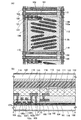
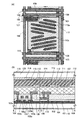
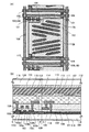
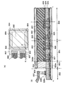
図1(A)は、本発明の第2の実施形態に係る液晶表示装置の構成を説明する為の平面図である。1画素分の画素を示している。この液晶表示装置は、FFS方式で液晶の配向方向を制御する装置である。図1(A)において、複数のソース配線108が互いに平行(図中縦方向に延伸)かつ互いに離間した状態で配置されている。複数のゲート配線105は、ソース配線108に略直交する方向(図中横方向)に延伸し、かつ互いに離間するように配置されている。補助配線106は、複数のゲート配線105それぞれに隣接する位置に配置されており、ゲート配線105に概略平行な方向、つまり、ソース配線108に概略直交する方向(図中左右方向)に延伸している。ソース配線108と、補助配線106及びゲート配線105とによって、略長方形の空間が囲まれ、この空間に液晶表示装置の画素電極が配置されている。画素電極を駆動する薄膜トランジスタ121は、図中左上の角に配置されている。画素電極及び薄膜トランジスタは、マトリクス状に複数配置されている。
(Second Embodiment)
FIG. 1A is a plan view for explaining a configuration of a liquid crystal display device according to a second embodiment of the present invention. A pixel for one pixel is shown. This liquid crystal display device is a device that controls the alignment direction of liquid crystal by the FFS method. In FIG. 1A, a plurality of source wirings 108 are arranged in parallel to each other (extending in the vertical direction in the drawing) and separated from each other. The plurality of
なお、ゲート配線105、補助配線106、及びソース配線108は、アルミニウム(Al)、タンタル(Ta)、チタン(Ti)、モリブデン(Mo)、タングステン(W)、ネオジウム(Nd)、クロム(Cr)、ニッケル(Ni)、白金(Pt)、金(Au)、銀(Ag)、銅(Cu)、マグネシウム(Mg)、スカンジウム(Sc)、コバルト(Co)、亜鉛(Zn)、ニオブ(Nb)、シリコン(Si)、リン(P)、ボロン(B)、ヒ素(As)、ガリウム(Ga)、インジウム (In)、錫(Sn)、酸素(O)で構成された群から選ばれた一つ又は複数の元素、もしくは、前記群から選ばれた一つ又は複数の元素を成分とする化合物や合金材料(例えば、インジウム錫酸化物(ITO)、インジウム亜鉛酸化物(IZO)、酸化珪素を添加したインジウム錫酸化物(ITSO)、酸化亜鉛(ZnO)、アルミネオジウム(Al−Nd)、マグネシウム銀(Mg−Ag)など)、もしくは、これらの化合物を組み合わせた物質などを有して形成される。もしくは、それらとシリコンの化合物(シリサイド)(例えば、アルミシリコン、モリブデンシリコン、ニッケルシリサイドなど)や、それらと窒素の化合物(例えば、窒化チタン、窒化タンタル、窒化モリブデン等)を有して形成される。なお、シリコン(Si)には、n型不純物(リンなど)やp型不純物(ボロンなど)を多く含んでいてもよい。これらの不純物を含むことにより、導電率が向上し、通常の導体と同様な振る舞いをするので、配線や電極として利用が容易となる。なお、シリコンは、単結晶でもよいし、多結晶(ポリシリコン)でもよいし、非晶質(アモルファスシリコン)でもよい。単結晶シリコンや多結晶シリコンを用いることにより、抵抗を小さくすることが出来る。非晶質シリコンを用いることにより、簡単な製造工程で作ることが出来る。なお、アルミニウムや銀は、導電率が高いため、信号遅延を低減することができ、エッチングしやすいので、加工しやすく、微細加工を行うことが出来る。なお、銅は、導電率が高いため、信号遅延を低減することが出来る。なお、モリブデンは、ITOやIZOなどの酸化物半導体や、シリコンと接触しても、材料が不良を起こすなどの問題が生じることなく製造でき、加工やエッチングが容易で、耐熱性が高いため、望ましい。なお、チタンは、ITOやIZOなどの酸化物半導体や、シリコンと接触しても、材料が不良を起こすなどの問題が生じることなく製造でき、また、耐熱性が高いため、望ましい。なお、タングステンは、耐熱性が高いため、望ましい。なお、ネオジウムは、耐熱性が高いため、望ましい。特に、ネオジウムとアルミニウムとの合金にすると、耐熱性が向上し、アルミニウムがヒロックをおこしにくくなるため、望ましい。なお、シリコンは、トランジスタが有する半導体膜と同時に形成でき、また、耐熱性が高いため、望ましい。なお、インジウム錫酸化物(ITO)、インジウム亜鉛酸化物(IZO)、酸化珪素を添加したインジウム錫酸化物(ITSO)、酸化亜鉛(ZnO)、シリコン(Si)は、透光性を有しているため、光を透過させるような部分に用いることができるため、望ましい。たとえば、画素電極や共通電極として用いることができる。
Note that the
なお、これらが単層で配線や電極を形成していてもよいし、多層構造になっていてもよい。単層構造で形成することにより、製造工程を簡略化することができ、工程日数を少なくでき、コストを低減することが出来る。また、多層構造にすることにより、それぞれの材料のメリットを生かし、デメリットを低減させ、性能の良い配線や電極を形成することが出来る。たとえば、抵抗の低い材料(アルミニウムなど)を多層構造の中に含むようにすることにより、配線の低抵抗化を図ることができる。また、耐熱性が高い材料を含むようにすれば、例えば、耐熱性が弱いが、別のメリットを有する材料を、耐熱性が高い材料で挟むような積層構造にすることにより、配線や電極全体として、耐熱性を高くすることが出来る。例えば、アルミニウムを含む層を、モリブデンやチタンを含む層で挟んだような形にした積層構造にすると望ましい。また、別の材料の配線や電極などと直接接するような部分がある場合、お互いに悪影響を及ぼすことがある。例えば、一方の材料が他方の材料の中に入っていって、性質を変えてしまい、本来の目的を果たせなくなったり、製造するときに、問題が生じて、正常に製造できなくなったりすることがある。そのような場合、ある層を別の層で挟んだり、覆ったりすることにより、問題を解決することが出来る。例えば、インジウム錫酸化物(ITO)と、アルミニウムを接触させたい場合は、間に、チタンやモリブデンを挟むことが望ましい。また、シリコンとアルミニウムを接触させたい場合は、間に、チタンやモリブデンを挟むことが望ましい。 In addition, these may form wiring and an electrode with a single layer, and may have a multilayer structure. By forming with a single layer structure, the manufacturing process can be simplified, the number of process days can be reduced, and the cost can be reduced. In addition, by using a multilayer structure, it is possible to take advantage of each material, reduce demerits, and form wiring and electrodes with good performance. For example, by including a low-resistance material (such as aluminum) in the multilayer structure, the resistance of the wiring can be reduced. In addition, if a material having high heat resistance is included, for example, a wiring or electrode as a whole can be obtained by forming a laminated structure in which a material having low merit is sandwiched between materials having another merit. As a result, the heat resistance can be increased. For example, it is preferable to form a layered structure in which a layer containing aluminum is sandwiched between layers containing molybdenum or titanium. In addition, if there is a portion that is in direct contact with a wiring or electrode of another material, it may adversely affect each other. For example, one material may be contained in the other material, changing its properties and failing to fulfill its original purpose, or producing a problem and making it impossible to manufacture normally. is there. In such a case, the problem can be solved by sandwiching or covering one layer with another layer. For example, when indium tin oxide (ITO) and aluminum are in contact with each other, it is desirable to sandwich titanium or molybdenum between them. In addition, when silicon and aluminum are to be brought into contact with each other, it is desirable to sandwich titanium or molybdenum between them.
なお、ゲート配線105の方が、ソース配線108よりも耐熱性が高い材料を用いることが望ましい。なぜなら、ゲート配線105の方が、製造工程の過程で、高い温度状態に配置されることが多いからである。
Note that the
なお、ソース配線108の方が、ゲート配線105よりも、抵抗の低い材料を用いることが望ましい。なぜなら、ゲート配線105には、H信号とL信号の2値の信号を与えるだけであるが、ソース配線108には、アナログの信号を与え、それが表示に寄与するからである。よって、ソース配線108には、正確な大きさの信号を供給できるようにするため、抵抗の低い材料を用いることが望ましい。
Note that the
なお、補助配線106を設けなくてもよいが、補助配線106を設けることにより、各画素における共通電極の電位を安定化させることができる。なお、図1では、補助配線106は、ゲート線と概略平行に配置されているが、これに限定されない。ソース配線108と概略平行に配置されていてもよい。その時は、ソース配線108と同じ材質で形成されることが望ましい。
Note that the
ただし、補助配線106は、ゲート線と概略平行に配置したほうが、開口率を大きくすることができ、効率的にレイアウトできるため、好適である。
However, it is preferable that the
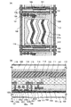
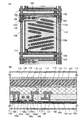
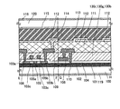
図1(B)は、図1(A)のE−F断面図及びG−H断面図である。図1(B)及び図1(A)に示すように、基板100の一部上には、液晶の配向方向を制御する第1の電極101が配置されている。ただし、基板100と第1の電極101との間に、別の層が配置されていても良い。
FIG. 1B is a cross-sectional view taken along the line EF and the line GH in FIG. As shown in FIGS. 1B and 1A, a
基板100は、ガラス基板、石英基板、アルミナなど絶縁物で形成される基板、後工程の処理温度に耐え得る耐熱性を有するプラスチック基板、シリコン基板、または金属基板である。また、ポリシリコンであってもよい。
The
なお、透過型の表示装置として動作させる場合は、基板100は、光透過性を有することが望ましい。
Note that in the case of operating as a transmissive display device, the
第1の電極101は、光透過性を有する導電膜(例えばITO(インジウム錫酸化物)膜、IZO(インジウム亜鉛酸化物)膜、ZnO膜、若しくは不純物が導入されたポリシリコン膜又はアモルファスシリコン膜)から形成されており、共通電極として機能する。なお、図1(A)に示すように、第1の電極101は、上下に繋がっている。このように繋げることにより、共通電極の抵抗を下げ、所定の電圧が加わりやすくすることが出来る。
The
第1の電極101上および基板100上には、絶縁膜102が形成されている。絶縁膜102は、基板100から不純物が拡散することを防止する膜であり、下地膜として機能する。絶縁膜102は、例えば、酸化シリコン(SiOx)、窒化シリコン(SiNx)、酸化窒化シリコン(SiOxNy:x>y)、窒化酸化シリコン(SiNxOy:x>y)など、酸素又は窒素を有する絶縁物質から形成される。また、これらの膜を複数積層した積層膜であってもよい。なお、基板100と第1の電極101の間に絶縁膜102と同じ機能を有する絶縁膜があってもよい。
An insulating
絶縁膜102上には半導体膜103が形成されている。半導体膜103には、薄膜トランジスタ121のソースとなる不純物領域103a、及びドレインとなる不純物領域103bが形成されている。不純物領域103a,103bは、例えばn型の不純物領域であるが、p型の不純物領域であってもよい。n型を付与する不純物としては、例えばリン(P)及びヒ素(As)があり、p型を付与する不純物としては、例えばボロン(B)及びガリウム(Ga)がある。
A
図1(A)の点線で示すように、第1の電極101は長方形の一角(図中左上の角)を欠いた形状であり、画素の略全面に形成されている。なお、長方形の角を欠いた部分101dには薄膜トランジスタ121が配置されている。この角を欠いた部分101dに薄膜トランジスタ121を配置することにより、画素内における表示に有効な領域を、より効率的に形成することができる。つまり、開口率の向上につながる。なお、半導体膜103は、例えばポリシリコン膜であるが、他の半導体膜(例えばアモルファスシリコン膜、単結晶シリコン膜、有機半導体膜、又はカーボンナノチューブ)であってもよい。
As shown by a dotted line in FIG. 1A, the
半導体膜103を覆うように、薄膜トランジスタ121のゲート絶縁膜104が形成されている。
A
ただし、ゲート絶縁膜104は、チャネル領域近傍にのみ配置され、それ以外の部分では、配置されていない場合もある。また、場所によって厚さや積層構造が異なる場合がある。例えば、チャネル近傍のみ厚かったり、層の数が多かったりして、それ以外の場所では、膜厚が薄かったり、層の数が少ない場合もある。このようにすることにより、ソース領域やドレイン領域への不純物の添加が制御しやすくなる。また、チャネル近傍のゲート絶縁膜104の厚さや層の数を変えることにより、半導体膜への不純物の添加量が場所によって変わるようにして、LDD領域を形成することが出来る。LDD領域を形成することにより、漏れ電流を低減させることや、ホットキャリアの発生を抑えて信頼性を向上させることが出来る。
However, the
ゲート絶縁膜104は、例えば、酸化シリコン(SiOx)、窒化シリコン(SiNx)、酸化窒化シリコン(SiOxNy:x>y)、窒化酸化シリコン(SiNxOy:x>y)など、酸素又は窒素を有する絶縁物質から形成される。また、これらの膜を複数積層した積層膜であってもよい。ゲート絶縁膜104上には半導体膜103の上方に位置するゲート電極105a,105bが形成されている。図1(B)及び図1(A)に示すように、ゲート電極105a,105bは補助配線106及びゲート配線105と同一配線層であり、ゲート配線105に電気的に接続している。ゲート電極105a,105bそれぞれの下方に位置する半導体膜103は、チャネル領域103cとして機能する。なお、2つのチャネル領域103c相互間に位置する半導体膜103にも、不純物領域103a,103bと同一の不純物が導入されている。なお、本実施形態においては、2つのゲート電極を有するマルチゲート構造としたが、本発明をこの構成に限定するものではない。
The
ゲート絶縁膜104上及びゲート電極105a,105b上には、第1層間絶縁膜107が形成されている。第1層間絶縁膜107には、無機材料又は有機材料を用いることができる。有機材料としては、ポリイミド、アクリル、ポリアミド、ポリイミドアミド、レジスト、シロキサン、又はポリシラザンなどを用いることができる。無機材料としては、酸化シリコン(SiOx)、窒化シリコン(SiNx)、酸化窒化シリコン(SiOxNy:x>y)、窒化酸化シリコン(SiNxOy:x>y)など、酸素又は窒素を有する絶縁物質を用いることができる。また、これらの膜を複数積層した積層膜であってもよい。また、有機材料と無機材料を組み合わせて積層膜にしてもよい。絶縁膜102、ゲート絶縁膜104、及び第1層間絶縁膜107には、不純物領域103a上に位置する接続孔、不純物領域103b上に位置する接続孔、第1の電極101上に位置する接続孔、及び補助配線106上に位置する接続孔が形成されている。第1層間絶縁膜107上には、ソース配線108、接続用導電膜109、及び接続用導電膜110が形成されている。
A first
なお、絶縁膜として無機材料を用いることにより、水分や不純物の侵入を止めることが出来る。特に、窒素を含む層を用いると、水分や不純物をブロックする機能が高い。 Note that entry of moisture and impurities can be stopped by using an inorganic material for the insulating film. In particular, when a layer containing nitrogen is used, the function of blocking moisture and impurities is high.
なお、絶縁膜として有機材料を用いることにより、表面を平坦にすることが出来る。そのため、その上の層に対して、よい効果をもたらすことが出来る。例えば、有機材料の上に形成する層も平坦にすることが出来るため、液晶の配向の乱れを防いだりすることが出来る。 Note that the surface can be flattened by using an organic material for the insulating film. Therefore, a good effect can be brought about on the layer above it. For example, since a layer formed over an organic material can be flattened, disorder of alignment of liquid crystals can be prevented.
ソース配線108は不純物領域103aの上方に位置しており、一部が接続孔に埋め込まれることにより不純物領域103aに電気的に接続している。したがって、ソース電極は、ソース配線108の一部となって存在していることとなる。接続用導電膜109は、一部が接続孔に埋め込まれることにより不純物領域103bに電気的に接続している。このように、接続用導電膜109を配置することにより、接続孔を深くあける必要がないので、正確に形成することが出来る。
The
ただし、図2(B)に示すように、第2の電極112と、不純物領域103bとを、図1(B)に示した接続用導電膜109を介さずに、直接接続してもよい。この場合、第2の電極112と、不純物領域103bとを接続するための接続孔は、深く開ける必要が出てくるが、接続用導電膜109が必要ないため、その領域を開口領域として画像表示に利用できる。そのため、開口率が向上し、低消費電力化をはかることが出来る。
However, as illustrated in FIG. 2B, the
接続用導電膜110は、補助配線106の上方に位置しており、一部が接続孔に埋め込まれることにより、補助配線106及び第1の電極101それぞれに電気的に接続している。このように、第1の電極101は、接続用導電膜110を介して補助配線106に電気的に接続している。なお、接続用導電膜110は複数設けられていてもよい。このようにすると、第1の電極101の電位が安定化する。また、接続用導電膜110を介して第1の電極101と補助配線106を接続することにより、接続孔を開ける回数を減らすことが出来るので、プロセス工程を簡略化することが出来る。
The connection
なお、接続用導電膜110は、ソース配線108と同時に、同じ材料を用いて形成したが、これに限定されない。第2の電極112と同時に、同じ材料を用いて形成してもよい。
Note that although the conductive film for
ソース配線108、接続用導電膜109、接続用導電膜110、及び第1層間絶縁膜107上には、第2層間絶縁膜111が形成されている。なお、第2層間絶縁膜111を形成しない構成としても良い。第2層間絶縁膜111には、無機材料又は有機材料を用いることができる。有機材料としては、ポリイミド、アクリル、ポリアミド、ポリイミドアミド、レジスト、又はシロキサン、ポリシラザンなどを用いることができる。無機材料としては、酸化シリコン(SiOx)、窒化シリコン(SiNx)、酸化窒化シリコン(SiOxNy:x>y)、窒化酸化シリコン(SiNxOy:x>y)など、酸素又は窒素を有する絶縁物質を用いることができる。また、これらの膜を複数積層した積層膜であってもよい。また、有機材料と無機材料を組み合わせて積層膜にしてもよい。第2層間絶縁膜111には、接続用導電膜109上に位置する接続孔が形成されている。
A second
第2層間絶縁膜111上には、液晶の配向方向を制御する第2の電極112が形成されている。第2の電極112は画素ごとに個別の電圧が供給される画素電極として機能し、ITO(インジウム錫酸化物)、ZnO(酸化亜鉛)、酸化インジウムに2〜20wt%のZnOを混合したターゲットを用いて形成されたIZO(インジウム亜鉛酸化物)などによって形成されている。第2の電極112は、一部が接続用導電膜109の上方に位置しており、この部分の一部が接続孔中に埋め込まれることにより、接続用導電膜109に電気的に接続している。このように、第2の電極112は、接続用導電膜109を介して薄膜トランジスタ121の不純物領域103bに電気的に接続している。
A
なお、図2に示すように、接続用導電膜109がない場合は、第2の電極112は、薄膜トランジスタ121の不純物領域103bに直接接続している。
Note that as shown in FIG. 2, in the case where the
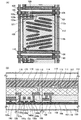
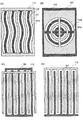
図2及び図1(A)に示すように、第2の電極112は略長方形であり、第1の電極101の上方に位置し、複数の開口パターン112a,112bを有している。開口パターン112a,112bの例としては、スリット状で互いに平行であるものを多く含む。本図に示す例では、開口パターン112a,112bの向きは、ソース配線108に対して斜めであるが、画素の図中上半分に位置する開口パターン112aと、下半分に位置する開口パターン112bの向きは互いに異なる。開口パターン112a,112bが形成されることにより、第1の電極101と第2の電極112の間で基板に平行な成分を有する電界が、第2の電極112の上方で生じる。このため、第2の電極112の電位を制御することにより、後述する液晶の配向方向を制御することができる。
As shown in FIGS. 2 and 1A, the
また、開口パターン112a,112bのように、開口パターンの向きが異なるものを配置することによって、液晶分子の動く方向が異なる領域を複数設けることが出来る。つまり、マルチドメイン構造にすることが出来る。マルチドメイン構造にすることにより、ある特定の方向から見たとき、画像の表示が正しくなくなってしまうことを防ぐことができ、その結果、視野角を向上させることが出来る。
In addition, by arranging the patterns with different opening patterns such as the opening
なお、開口パターンの形状は本実施形態の形状に限定されない。第3の実施形態以降で記載する開口パターンの形状も適用することができる。すなわち開口パターンには、例えば櫛歯形状の電極における櫛歯部分の相互間のスペース等、導電体パターンが形成されていないスペースを含まれるものとする。 The shape of the opening pattern is not limited to the shape of this embodiment. The shape of the opening pattern described in the third and subsequent embodiments can also be applied. That is, the opening pattern includes a space in which no conductor pattern is formed, such as a space between comb teeth portions of a comb-shaped electrode.
また、図1(A)に示すように、基板100に対して垂直な方向から見た場合に、共通電極として機能する第1の電極101が、画素電極として機能する第2の電極112の外側に食み出している。このようにすることにより、信号を受け取った後フローティング状態になった第2の電極112が、ソース配線108を介して他の画素へ伝達される信号の影響を受けることが抑制される。その結果、クロストークなどの画像不良を低減することが出来る。なお、本発明はこのような電極構造に限定されるものではなく、共通電極が画素電極の内側に配置される部分を有していても良い。
In addition, as illustrated in FIG. 1A, when viewed from a direction perpendicular to the
第2層間絶縁膜111上及び第2の電極112上には、第1配向膜113及び液晶114が積層されている。液晶114としては、強誘電性液晶(FLC)、ネマティック液晶、スメクティック液晶、ホモジニアス配向になるような液晶、ホメオトロピック配向になるような液晶などを用いることができる。液晶114上には、第2配向膜115及びカラーフィルタ116を介して対向基板120が配置されている。なお、基板100及び対向基板120それぞれには、偏光板119,118が設けられている。
A
なお、偏光板のほかに、位相差板やλ/4板などが配置されている場合も多い。 In addition to the polarizing plate, a retardation plate, a λ / 4 plate, or the like is often disposed.
なお、上記した構成において、第1の電極101、第2の電極112のうち開口パターンが形成されていない部分、及びこれらの相互間に位置する各絶縁膜によって、容量が形成される。この容量が形成されることにより保持容量が大きくなる。
Note that in the above structure, a capacitor is formed by the portion of the
次に、本発明の半導体装置、液晶表示装置の製造方法の一例について説明する。まず、基板100上に光透過性を有する導電膜(例えばITO(インジウム錫酸化物)膜、IZO膜、ZnO膜、又はSi膜)を形成する。次いで、この導電膜上にフォトレジスト膜(図示せず)を形成し、このフォトレジスト膜を露光及び現像する。これにより、導電膜上にはレジストパターンが形成される。次いで、このレジストパターンをマスクとして導電膜をエッチングする。これにより、導電膜が選択的に除去され、基板100上には第1の電極101が形成される。その後、レジストパターンを除去する。
Next, an example of a method for manufacturing the semiconductor device and the liquid crystal display device of the present invention will be described. First, a light-transmitting conductive film (for example, an ITO (indium tin oxide) film, an IZO film, a ZnO film, or a Si film) is formed over the
次いで、基板100上及び第1の電極101上に、絶縁膜102を形成する。絶縁膜102は、後述するゲート絶縁膜104より厚く形成されることが望ましい。次いで、絶縁膜102上に半導体膜(例えばポリシリコン膜)を形成し、この半導体膜を、レジストパターンを用いたエッチングにより選択的に除去する。これにより、絶縁膜102上には島状の半導体膜103が形成される。
Next, the insulating
次いで、半導体膜103上及び絶縁膜102上に、ゲート絶縁膜104を形成する。ゲート絶縁膜104は例えば酸化窒化シリコン膜又は酸化シリコン膜であり、プラズマCVD法により形成される。なお、ゲート絶縁膜104を窒化シリコン膜、若しくは窒化シリコン及び酸化シリコンを有する多層膜により形成してもよい。次いで、ゲート絶縁膜104上に導電膜を形成し、この導電膜を、レジストパターンをマスクとしたエッチングを行うことにより、選択的に除去する。これにより、半導体膜103上に位置するゲート絶縁膜104上には、ゲート電極105a,105bが形成される。また、本工程により、ゲート配線105及び補助配線106が形成される。
Next, the
なお、上記したように補助配線106を設けることにより、各画素において第1の電極101の電位を安定化させることができる。また、補助配線106を形成しなくてもよい。また、補助配線106を他の層(例えばソース配線108と同一の層、又は第1の電極101と同一の層、又は第2の電極112と同一の層)に設けてもよく、複数の層に分けて形成してもよい。また、図1(B)において補助配線106は、ソース配線108に直交する方向に延伸しているが、ソース配線108と同一方向に延伸する構成であってもよい。
Note that by providing the
なお、導電膜は、アルミニウム(Al)、タンタル(Ta)、チタン(Ti)、モリブデン(Mo)、タングステン(W)、ネオジウム(Nd)、クロム(Cr)、ニッケル(Ni)、白金(Pt)、金(Au)、銀(Ag)、銅(Cu)、マグネシウム(Mg)、スカンジウム(Sc)、コバルト(Co)、亜鉛(Zn)、ニオブ(Nb)、シリコン(Si)、リン(P)、ボロン(B)、ヒ素(As)、ガリウム(Ga)、インジウム(In)、錫(Sn)、酸素(O)で構成された群から選ばれた一つ又は複数の元素、もしくは、前記群から選ばれた一つ又は複数の元素を成分とする化合物や合金材料(例えば、インジウム錫酸化物(ITO)、インジウム亜鉛酸化物(IZO)、酸化珪素を添加したインジウム錫酸化物(ITSO)、酸化亜鉛(ZnO)、アルミネオジウム(Al−Nd)、マグネシウム銀(Mg−Ag)など)、もしくは、これらの化合物を組み合わせた物質などを有して形成される。もしくは、それらとシリコンの化合物(シリサイド)(例えば、アルミシリコン、モリブデンシリコン、ニッケルシリサイドなど)や、それらと窒素の化合物(例えば、窒化チタン、窒化タンタル、窒化モリブデン等)を有して形成される。なお、シリコン(Si)には、n型不純物(リンなど)やp型不純物(ボロンなど)を多く含んでいてもよい。 The conductive film is made of aluminum (Al), tantalum (Ta), titanium (Ti), molybdenum (Mo), tungsten (W), neodymium (Nd), chromium (Cr), nickel (Ni), platinum (Pt). , Gold (Au), silver (Ag), copper (Cu), magnesium (Mg), scandium (Sc), cobalt (Co), zinc (Zn), niobium (Nb), silicon (Si), phosphorus (P) One or more elements selected from the group consisting of boron (B), arsenic (As), gallium (Ga), indium (In), tin (Sn), and oxygen (O), or the group Compound or alloy material containing one or more elements selected from (for example, indium tin oxide (ITO), indium zinc oxide (IZO), indium tin oxide to which silicon oxide is added (ITSO)) Zinc oxide (ZnO), aluminum neodymium (Al-Nd), magnesium silver (Mg-Ag), etc.), or is formed with a like material that combines these compounds. Alternatively, a silicon compound (silicide) (for example, aluminum silicon, molybdenum silicon, nickel silicide, or the like) or a nitrogen compound (for example, titanium nitride, tantalum nitride, molybdenum nitride, or the like) is formed. . Note that silicon (Si) may contain a large amount of n-type impurities (such as phosphorus) and p-type impurities (such as boron).
なお、これらが単層で配線や電極を形成していてもよいし、多層構造になっていてもよい。単層構造で形成することにより、製造工程を簡略化することができ、工程日数を少なくでき、コストを低減することが出来る。また、多層構造にすることにより、それぞれの材料のメリットを生かし、デメリットを低減させ、性能の良い配線や電極を形成することが出来る。たとえば、抵抗の低い材料(アルミニウムなど)を多層構造の中に含むようにすることにより、配線の低抵抗化を図ることができる。また、耐熱性が高い材料を含むようにすれば、例えば、耐熱性が弱いが、別のメリットを有する材料を、耐熱性が高い材料で挟むような積層構造にすることにより、配線や電極全体として、耐熱性を高くすることが出来る。例えば、アルミニウムを含む層を、モリブデンやチタンを含む層で挟んだような形にした積層構造にすると望ましい。また、別の材料の配線や電極などと直接接するような部分がある場合、お互いに悪影響を及ぼすことがある。例えば、一方の材料が他方の材料の中に入っていって、性質を変えてしまい、本来の目的を果たせなくなったり、製造するときに、問題が生じて、正常に製造できなくなったりすることがある。そのような場合、ある層を別の層で挟んだり、覆ったりすることにより、問題を解決することが出来る。例えば、インジウム錫酸化物(ITO)と、アルミニウムを接触させたい場合は、間に、チタンやモリブデンを挟むことが望ましい。また、シリコンとアルミニウムを接触させたい場合は、間に、チタンやモリブデンを挟むことが望ましい。 In addition, these may form wiring and an electrode with a single layer, and may have a multilayer structure. By forming with a single layer structure, the manufacturing process can be simplified, the number of process days can be reduced, and the cost can be reduced. In addition, by using a multilayer structure, it is possible to take advantage of each material, reduce demerits, and form wiring and electrodes with good performance. For example, by including a low-resistance material (such as aluminum) in the multilayer structure, the resistance of the wiring can be reduced. In addition, if a material having high heat resistance is included, for example, a wiring or electrode as a whole can be obtained by forming a laminated structure in which a material having low merit is sandwiched between materials having another merit. As a result, the heat resistance can be increased. For example, it is preferable to form a layered structure in which a layer containing aluminum is sandwiched between layers containing molybdenum or titanium. In addition, if there is a portion that is in direct contact with a wiring or electrode of another material, it may adversely affect each other. For example, one material may be contained in the other material, changing its properties and failing to fulfill its original purpose, or producing a problem and making it impossible to manufacture normally. is there. In such a case, the problem can be solved by sandwiching or covering one layer with another layer. For example, when indium tin oxide (ITO) and aluminum are in contact with each other, it is desirable to sandwich titanium or molybdenum between them. In addition, when silicon and aluminum are to be brought into contact with each other, it is desirable to sandwich titanium or molybdenum between them.
次いで、ゲート電極105a,105bをマスクとして、半導体膜103に不純物を注入する。これにより、半導体膜103には、不純物領域103a,103b、及びゲート電極105a,105b相互間に位置する不純物領域が形成される。なお、n型、p型の不純物元素を個別に注入してもよいし、特定の領域にはn型の不純物元素及びp型の不純物元素を共に注入してもよい。ただし後者の場合には、n型の不純物元素又はp型の不純物元素のどちらか一方の注入量が多くなるようにする。なお、本工程において、レジストパターンをマスクとして用いてもよい。
Next, impurities are implanted into the
なお、このとき、ゲート絶縁膜104の厚さや積層構造を変えることにより、LDD領域を形成してもよい。LDD領域を形成したい部分は、ゲート絶縁膜104を厚く形成することや、層の数を増やすことをすればよい。その結果、不純物の注入量が減るため、LDD領域を容易に形成することが出来る。
Note that at this time, the LDD region may be formed by changing the thickness or the stacked structure of the
なお、半導体膜103に不純物を注入する場合、ゲート電極105a,105bを形成する前、例えば、ゲート絶縁膜104を成膜する前や、成膜した後に行っても良い。その場合は、レジストパターンをマスクとして用いて、形成する。これにより、ゲートと同じ層の電極と、不純物が注入された半導体膜との間で、容量を形成することが出来る。ゲートと同じ層の電極と、不純物が注入された半導体膜との間には、ゲート絶縁膜が配置されているので、膜厚がうすく、大きな容量を形成することが出来る。
Note that the impurity may be implanted into the
次いで、第1層間絶縁膜107及び各接続孔を形成する。次いで、第1層間絶縁膜107上及び各接続孔中に導電膜(例えば金属膜)を形成し、この導電膜を、レジストパターンを用いたエッチングにより選択的に除去する。これにより、ソース配線108、接続用導電膜109、及び接続用導電膜110が形成される。
Next, the first
次いで、第2層間絶縁膜111及び各接続孔を形成する。次いで、第2層間絶縁膜111上及び各接続孔中に光透過性を有する導電膜(例えばITO膜、IZO膜、ZnO膜、又はSi膜)を形成し、この導電膜を、レジストパターンを用いたエッチングにより選択的に除去する。これにより、第2の電極112が形成される。
Next, the second
なお、接続用導電膜109の一部が埋め込まれている接続孔と、第2の電極112の一部が埋め込まれている接続孔とは位置が互いに異なっている。このようにすることにより、接続用導電膜109及び第2の電極112のうち、接続孔上に位置する部分が窪んでも、この窪みが重なることはない。このため、第2の電極112に深く窪む部分が形成されず、上記したレジストパターンの不良が発生することを抑制できる。その後、レジストパターンを除去する。
Note that the position of the connection hole in which part of the connection
次いで、第1配向膜113を形成し、第2配向膜115が形成された対向基板120との間に液晶114を封止する。その後、液晶114と接しない側の対向基板120や基板100に、偏光板118,119、位相差板(図示せず)、λ/4板等の光学フィルム(図示せず)、拡散板やプリズムシート等の光学フィルム等を設ける。さらに、バックライトやフロントライトを設ける。バックライトとしては、直下型やサイドライト型を用いることが出来る。光源としては、冷陰極管やLED(発光ダイオード)を用いることができる。LEDとしては、白色LEDや、色ごとのLED(例えば、白、赤、青、緑、シアン、マゼンタ、イエローなど)を組み合わせて用いればよい。LEDを用いると、光の波長のピークが鋭いため、色純度を上げることが出来る。サイドライト型の場合は、導光板を配置し、均一な面光源を実現する。このようにして、液晶表示装置が形成される。
Next, the
なお、液晶表示装置とは、基板と対向基板と、それに挟まれた液晶のみの部分を呼んでも良い。さらに、液晶表示装置とは、偏光板や位相差板などの光学フィルムを配置したものまで含む場合もあり、その他にも、拡散板やプリズムシートや光源(冷陰極管やLEDなど)や導光板などを含めてもよい。 Note that the liquid crystal display device may refer to a substrate, a counter substrate, and only a portion of liquid crystal sandwiched therebetween. In addition, the liquid crystal display device may include an optical film such as a polarizing plate or a retardation plate. In addition, a diffusion plate, a prism sheet, a light source (such as a cold cathode tube or an LED), or a light guide plate. Etc. may be included.
以上、本発明の第2の実施形態によれば、FFS方式で液晶の配向方向を制御する液晶表示装置において、第1の電極101を基板100上すなわち絶縁膜102の下に配置している。このため、第1の電極101を絶縁膜102上に配置する場合と比較して、第1の電極101と第2の電極112の間隔を広げることができる。従って、第1の電極101と第2の電極112の間隔の自由度が向上する。その結果、画素電極が有する開口パターンの配置間隔や開口パターンの幅は、画素電極と共通電極との間の距離によって、最適値が変わってくるため、開口パターンの大きさや幅や間隔も自由に設定することができる。そして、電極間に加わる電界の勾配を制御することができるようになり、例えば基板と平行方向の電界を増やすこと等を容易に行うことができる。すなわち、液晶を用いた表示装置においては、基板と平行に配向している液晶分子(いわゆるホモジニアス配向)を、基板と平行な方向で制御できるため、最適な電界を加えることで、視野角が広くなる。
As described above, according to the second embodiment of the present invention, in the liquid crystal display device that controls the alignment direction of the liquid crystal by the FFS method, the
また、絶縁膜102の膜厚を変えても、トランジスタの動作などに影響を与えないため、自由に厚さを制御出来る。そのため、第1の電極101と第2の電極112の間隔を自由に広げることが出来る。
In addition, even if the thickness of the insulating
また、絶縁膜102を厚くすることにより、ゲート絶縁膜104を薄くしても、第1の電極101と第2の電極112の間隔を広くして、液晶114に適切な電界をかけることができる。ゲート絶縁膜104を薄くした場合、薄膜トランジスタ121の電流駆動能力を向上させることができ、かつゲート容量を向上させることができる。
In addition, by increasing the thickness of the insulating
また、ゲート電極105aとゲート配線105は別の層に形成されていてもよいし、別の材料で形成されていてもよい。
Further, the
なお、接続用導電膜109を、ソース配線108と同一層に配置したが、他の配線層(例えばゲート配線105、第1の電極101、又は第2の電極112と同一層)に配置してもよい。また、ゲート絶縁膜104は全面に形成されていなくてもよい。
Note that although the connection
また、第2の電極112の一部が埋め込まれた接続孔を、接続用導電膜109の一部が埋め込まれた接続孔と重なる位置に形成しても良い。この場合、1つの場所に収めることが出来るため、効率的にレイアウトすることが出来る。そのため、画素の開口率を向上させることができる。
Alternatively, the connection hole in which part of the
また、本実施形態では、チャネル領域の上方にゲート電極を配置した、いわゆるトップゲート型の薄膜トランジスタについて説明をしたが、本発明は特にこれに限定されるものではない。チャネル領域の下方にゲート電極が配置された、いわゆるボトムゲート型の薄膜トランジスタにしてもよいし、チャネル領域の上下にゲート電極が配置された構造を有するトランジスタを形成してもよい。 In this embodiment, a so-called top-gate thin film transistor in which a gate electrode is disposed above a channel region has been described, but the present invention is not particularly limited thereto. A so-called bottom-gate thin film transistor in which a gate electrode is disposed below a channel region may be used, or a transistor having a structure in which gate electrodes are disposed above and below a channel region may be formed.
また、液晶表示装置は透過型であってもよいし、半透過型又は反射型の液晶表示装置であってもよい。半透過型の液晶表示装置は、例えば第1の電極101を光透過性の膜(例えばITO(インジウム錫酸化物)膜、IZO(インジウム亜鉛酸化物)膜、ZnO膜、若しくは不純物が導入されたポリシリコン膜又はアモルファスシリコン膜)により形成し、第2の電極112を金属膜により形成することにより実現できる。また、第2の電極112を光透過性の膜により形成し、かつ第1の電極101の一部を金属膜により形成して残りを光透過性の膜により形成しても、半透過型の液晶表示装置を実現できる。また反射型の液晶表示装置においては、第1の電極101を金属膜にすることで、第1の電極101に反射板の機能を持たせることができる。また基板100と第1の電極101の間に絶縁膜(例えば酸化シリコン膜)を設け、この絶縁膜中に反射膜としての金属膜を形成することもできる。さらに、基板100の外側の面に、反射膜としての反射シート(例えばアルミニウム膜)を設けることもできる。なお、ここで述べた内容は、後述する各実施形態にも同様に適用できる。
The liquid crystal display device may be a transmissive liquid crystal display device, a transflective liquid crystal display device, or a reflective liquid crystal display device. In the transflective liquid crystal display device, for example, a light transmissive film (for example, an ITO (indium tin oxide) film, an IZO (indium zinc oxide) film, a ZnO film, or an impurity) is introduced into the
(第3の実施形態)
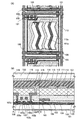
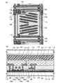
図3(A)は、第3の実施形態に係る液晶表示装置の構成を説明する為の平面図である。図3(B)は、図3(A)のE−F断面図及びG−H断面図である。本実施形態は、第1の電極101が薄膜トランジスタ121の不純物領域103bに電気的に接続されていて画素電極として機能している点、第2の電極112が補助配線106に電気的に接続されていて共通電極として機能している点、基板100に対して垂直な方向から見た場合に第2の電極112が第1の電極101の外側に食み出している点、並びに、第1の電極101及び第2の電極112と各配線の接続構造を除いて、第2の実施形態と概ね同様の構成である。また、本実施形態に係る液晶表示装置の製造方法は、第2の実施形態と略同様である。従って、第2の実施形態で述べた内容は、本実施形態にも適用することが可能である。以下、第2の実施形態と同様の構成の部分については同一の符号を付し、説明を省略する。
(Third embodiment)
FIG. 3A is a plan view for explaining the configuration of the liquid crystal display device according to the third embodiment. FIG. 3B is a cross-sectional view taken along the line EF and the line GH in FIG. In this embodiment, the
本実施形態において、第1層間絶縁膜107、ゲート絶縁膜104、及び絶縁膜102には、第1の電極101上に位置する接続孔が形成されており、第1層間絶縁膜107及びゲート絶縁膜104には、薄膜トランジスタ121の不純物領域103a,103b上に位置する接続孔が形成されている。また、第1層間絶縁膜107には、補助配線106上に位置する接続孔が形成されている。
In the present embodiment, a connection hole located on the
接続用導電膜109は、不純物領域103bの上方から第1の電極101の上方まで延伸しており、一部が接続孔に埋め込まれることにより、不純物領域103b及び第1の電極101それぞれに電気的に接続している。このように、第1の電極101は、接続用導電膜109を介して不純物領域103bに電気的に接続している。また、接続用導電膜110は、一部が接続孔に埋め込まれることにより補助配線106に電気的に接続している。
The connection
なお、第1の電極101は、第2の電極112と同じ層で形成された接続用導電膜を設けて、それを介して不純物領域103bと電気的に接続してもよい。
Note that the
また、第2層間絶縁膜111には、接続用導電膜110上に位置する接続孔が形成されている。第2の電極112は、一部が接続孔に埋め込まれることにより接続用導電膜110に電気的に接続している。このように、第2の電極112は接続用導電膜110を介して補助配線106に電気的に接続している。なお、図3(A)に示すように、上下に位置する第2の電極112同士は、部分的に互いに繋がっている。
In addition, a connection hole located on the connection
なお、接続用導電膜110を配置せずに、補助配線106と第2の電極112とが、直接接続されていてもよい。
Note that the
なお、本実施形態では、接続用導電膜110は、第1の電極101が有する4つの角のうち、薄膜トランジスタの近くの角を除く3つの角の上方それぞれに形成されている。
In this embodiment, the connection
本実施形態によっても、第2の実施形態と同様の効果を得ることができる。なお、本実施形態において、接続用導電膜110を設けなくてもよい。この場合、第1及び第2層間絶縁膜107,111には、補助配線106上に位置する接続孔が形成される。そして、この接続孔に第2の電極112の一部が埋め込まれることにより、補助配線106と第2の電極112が電気的に接続される。この場合、開口率を向上させることができる。ただし、接続用導電膜110を設けると、第1及び第2層間絶縁膜107,111それぞれに形成された接続孔に位置ずれが生じても、この位置ずれを接続用導電膜110によって吸収することができる。
According to this embodiment, the same effect as that of the second embodiment can be obtained. In this embodiment, the connection
また、図3に示すように、第1の電極101が画素電極として機能し、第2の電極112が共通電極として機能し、画素電極よりも、共通電極の方が液晶と近接して配置されている。その結果、画素ごとに画素電極の電圧が変化しても、共通電極の電圧は一定であるため、液晶が存在する部分の電界は隣接する画素からの影響を受けにくく、クロストークを低減できる。例えば、表示する画像によっては、隣接する画素に入力される信号が大きく異なる場合があるが、本実施形態のように共通電極を液晶と近接して配置する構成を採用することで、クロストークを防ぐことが可能となる。
As shown in FIG. 3, the
なお、図3では画素を一つのみ図示したが、実際には複数の画素がマトリックス状に配置されている。この場合、各画素の第2の電極112を相互に接続してもよい。このようにすることにより、抵抗を低くし、第2の電極112に電圧が十分に加わるようにすることができる。
Although only one pixel is shown in FIG. 3, a plurality of pixels are actually arranged in a matrix. In this case, the
なお、本実施形態は、第2の実施形態で述べた内容を、一部変更、改良、又は変形した場合の一例を示している。したがって、第2の実施形態で述べた内容は、本実施形態にも適用することや、組み合わせることが出来る。 In addition, this embodiment has shown an example at the time of having partially changed, improved, or changed the content described in 2nd Embodiment. Therefore, the contents described in the second embodiment can be applied to or combined with this embodiment.
また、さまざまな図を用いて述べてきたが、1つの図は、様々な構成要件により成り立っている。したがって、各々の図の中から、各々の構成要件に関して、組み合わせて、さらなる構成を作ることも可能である。 Further, although various figures have been described, one figure is constituted by various constituent requirements. Therefore, it is also possible to combine the components in the respective drawings to make further configurations.
(第4の実施形態)
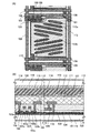
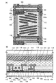
図4(A)は、本発明の第4の実施形態に係る液晶表示装置の構成を説明する為の平面図であり、図4(B)は、図4(A)のA−B断面図及びC−D断面図である。本実施形態に係る液晶表示装置は第2の電極112に形成された開口パターン112cの形状が異なる点、及び第1の電極101に開口パターン101aが形成されている点を除いて、第3の実施形態と同様の構成である。すなわち本実施形態に係る液晶表示装置は、IPS方式で液晶の配向方向を制御する装置であり、液晶表示装置に対して垂直な方向から見た場合に、画素電極及び共通電極が主要部分で互い違いかつ略平行となっている。FFS方式では、画素電極及び共通電極のうち下方に位置する電極は開口パターンを有していない。また、本実施形態に係る液晶表示装置の製造方法は、第3の実施形態と概ね同様である。従って、第3の実施形態で述べた内容は、本実施の形態にも適用することが可能である。なお、第2の実施形態で述べた内容は、第3の実施形態でも適用可能であるため、第4の実施形態にも適用可能である。以下、第3の実施形態と同様の構成の部分については同一の符号を付し、説明を省略する。
(Fourth embodiment)
FIG. 4A is a plan view for explaining the configuration of the liquid crystal display device according to the fourth embodiment of the present invention, and FIG. 4B is a cross-sectional view taken along the line AB of FIG. And C-D sectional view. The liquid crystal display device according to the present embodiment is the same as that of the third embodiment except that the shape of the
開口パターン112c,101aは、それぞれ図4(A)中上下にジグザグに延伸している。開口パターン101aは、第2の電極112のうち開口パターン112cが形成されていない領域の下方及びその周囲に位置している。
Each of the opening
また、開口パターン112c,101aのように、開口パターンの向きが異なるものを配置することによって、液晶分子の動く方向が異なる領域を複数設けることが出来る。つまり、マルチドメイン構造にすることが出来る。マルチドメイン構造にすることにより、ある特定の方向から見たとき、画像の表示が正しくなくなってしまうことを防ぐことができ、その結果、視野角を向上させることが出来る。
In addition, by arranging the patterns with different opening patterns such as the opening
本実施形態によっても、第3の実施形態と同様の効果を得ることができる。なお、本実施形態において、第2の電極112の形状及び開口パターン112cの形状、並びに第1の電極101及び開口パターン101aの形状を、第2の実施形態における第2の電極112の形状及び開口パターン112cの形状にしてもよい。ただし、基板100に対して垂直な方向から見た場合に、開口パターン101a,112cは、第1の電極101及び第2の電極112の周辺部分を除いて互い違いかつ略平行になるように配置される必要がある。ただし、これに限定されない。
According to this embodiment, the same effect as that of the third embodiment can be obtained. Note that in this embodiment, the shape of the
また、第2の実施形態又は第3の実施形態に示したFFS方式の液晶表示装置において、第2の電極112の形状及び開口パターン112a,112bの形状を、本実施形態で示した形状にしてもよい。
In the FFS mode liquid crystal display device shown in the second embodiment or the third embodiment, the shape of the
また、第1の電極101と、第2の電極112や補助配線106とをオーバーラップさせることにより、容量を形成することができ、それを保持容量として用いることができる。
In addition, by overlapping the
なお、本実施形態は、第2〜第3の実施形態で述べた内容を、一部変更、改良、又は変形した場合の一例を示している。したがって、第2〜第3の実施形態で述べた内容は、本実施形態にも適用することや、組み合わせることが出来る。 In addition, this embodiment has shown an example at the time of having partially changed, improved, or deformed the content described in the second to third embodiments. Therefore, the contents described in the second to third embodiments can be applied to or combined with this embodiment.
また、さまざまな図を用いて述べてきたが、1つの図は、様々な構成要件により成り立っている。したがって、各々の図の中から、各々の構成要件に関して、組み合わせて、さらなる構成を作ることも可能である。 Further, although various figures have been described, one figure is constituted by various constituent requirements. Therefore, it is also possible to combine the components in the respective drawings to make further configurations.
(第5の実施形態)
図5(A)は、本発明の第5の実施形態に係るIPS方式の液晶表示装置の構成を説明する為の平面図である。図5(B)は、図5(A)のA−B断面図及びC−D断面図である。本実施形態は、第1の電極101が補助配線106に電気的に接続されていて共通電極として機能している点、第2の電極112が接続用導電膜109に電気的に接続されていて画素電極として機能している点、並びに、第1の電極101及び第2の電極112と各配線の接続構造を除いて、第4の実施形態と同様の構成である。また、本実施形態に係る液晶表示装置の製造方法は、第4の実施形態と略同様である。以下、第4の実施形態と同様の構成の部分については同一の符号を付し、説明を省略する。
(Fifth embodiment)
FIG. 5A is a plan view for explaining the configuration of an IPS liquid crystal display device according to the fifth embodiment of the present invention. 5B is a cross-sectional view taken along a line AB and a line CD in FIG. 5A. In this embodiment, the
従って、第1の実施形態乃至第4の実施形態で述べた内容は、本実施形態に対しても適用することが可能である。 Therefore, the contents described in the first to fourth embodiments can be applied to this embodiment.
本実施形態において、第3の実施形態に示した接続用導電膜110は形成されていない。その代わり、ゲート絶縁膜104及び絶縁膜102には、第1の電極101上に位置する接続孔が形成されている。補助配線106は、一部がこの接続孔に埋め込まれることにより、第1の電極101に電気的に接続している。
In the present embodiment, the connection
なお、この接続孔は、ゲート電極105a,105bを形成する前に形成する。
This connection hole is formed before the
このように配置することにより、効率的にレイアウトをすることができ、開口率を向上させることが出来る。 By arranging in this way, the layout can be efficiently performed and the aperture ratio can be improved.
また、第2層間絶縁膜111には、接続用導電膜110上に位置する接続孔は形成されておらず、その代わりに接続用導電膜109上に位置する接続孔が形成されている。第2の電極112は、この接続孔に一部が埋め込まれることにより、接続用導電膜109に電気的に接続している。
In addition, the second
なお、第2の電極112が接続用導電膜109に電気的に接続されているが、これに限定されない。接続用導電膜109を配置せず、不純物領域103bと電気的に接続されていてもよい。
Note that although the
なお、本実施形態において、第2の電極112の形状及び開口パターン112cの形状、並びに第1の電極101及び開口パターン101aの形状を、第2の実施形態における第2の電極112の形状及び開口パターン112cの形状にしてもよい。ただし、基板100に対して垂直な方向から見た場合に、開口パターン101a,112cは、第1の電極101及び第2の電極112の周辺部分を除いて互い違いかつ略平行になるように配置される必要がある。
Note that in this embodiment, the shape of the
また、開口パターン112c,101aのように、開口パターンの向きが異なるものを配置することによって、液晶分子の動く方向が異なる領域を複数設けることが出来る。つまり、マルチドメイン構造にすることが出来る。マルチドメイン構造にすることにより、ある特定の方向から見たとき、画像の表示が正しくなくなってしまうことを防ぐことができ、その結果、視野角を向上させることが出来る。
In addition, by arranging the patterns with different opening patterns such as the opening
なお、本実施形態は、第2〜第4の実施形態で述べた内容を、一部変更、改良、又は変形した場合の一例を示している。したがって、第2〜第4の実施形態で述べた内容は、本実施形態にも適用することや、組み合わせることが出来る。 In addition, this embodiment has shown an example at the time of having partially changed, improved, or deform | transformed the content described in the 2nd-4th embodiment. Therefore, the contents described in the second to fourth embodiments can be applied to or combined with this embodiment.
また、さまざまな図を用いて述べてきたが、1つの図は、様々な構成要件により成り立っている。したがって、各々の図の中から、各々の構成要件に関して、組み合わせて、さらなる構成を作ることも可能である。 Further, although various figures have been described, one figure is constituted by various constituent requirements. Therefore, it is also possible to combine the components in the respective drawings to make further configurations.
(第6の実施形態)
図6(A)は、本発明の第6の実施形態に係るFFS方式の液晶表示装置の構成を説明する為の平面図である。図6(B)は、図6(A)のE−F断面図及びG−H断面図である。本実施形態は、ソース配線108が屈曲している点、ソース配線108に合わせて第1の電極101及び第2の電極112も屈曲している点、及び第2の電極112が有する開口パターン112hがソース配線108に沿って延伸し、かつ屈曲している点を除いて、第2の実施形態に示したFFS方式の液晶表示装置と同様の構成である。このため、第2の実施形態で説明した内容は本実施形態にも適用することができる。以下、第2の実施形態と同様の構成の部分については同一の符号を付し、説明を省略する。
(Sixth embodiment)
FIG. 6A is a plan view for explaining the configuration of the FFS mode liquid crystal display device according to the sixth embodiment of the present invention. 6B is a cross-sectional view taken along a line EF and a line GH in FIG. 6A. In this embodiment, the
従って、第2の実施形態乃至第5の実施形態で述べた内容は、本実施形態に対しても適用することが可能である。 Therefore, the contents described in the second to fifth embodiments can be applied to this embodiment.
図6の開口パターン112hのように、開口パターンの向きが異なるものを配置することによって、液晶分子の動く方向が異なる領域を複数設けることが出来る。つまり、マルチドメイン構造にすることが出来る。マルチドメイン構造にすることにより、ある特定の方向から見たとき、画像の表示が正しくなくなってしまうことを防ぐことができ、その結果、視野角を向上させることが出来る。
A plurality of regions having different directions of movement of liquid crystal molecules can be provided by arranging those having different orientations of the opening pattern, such as the
さらに、開口パターン112hにそって、ソース配線108も屈曲しているため、効率的にレイアウトをすることができ、開口率を向上させることが出来る。
Furthermore, since the
本実施形態によっても第2の実施形態と同様の効果を得ることができる。なお、本実施形態において第2の電極112が有する開口パターンの形状を、第2又は第4の実施形態で示した形状にしてもよい。
According to this embodiment, the same effect as that of the second embodiment can be obtained. In this embodiment, the shape of the opening pattern of the
なお、本実施形態は、第2〜第5の実施形態で述べた内容を、一部変更、改良、又は変形した場合の一例を示している。したがって、第2〜第5の実施形態で述べた内容は、本実施形態にも適用することや、組み合わせることが出来る。 In addition, this embodiment has shown an example at the time of having partially changed, improved, or changed the content described in the 2nd-5th embodiment. Therefore, the contents described in the second to fifth embodiments can be applied to or combined with this embodiment.
また、さまざまな図を用いて述べてきたが、1つの図は、様々な構成要件により成り立っている。したがって、各々の図の中から、各々の構成要件に関して、組み合わせて、さらなる構成を作ることも可能である。 Further, although various figures have been described, one figure is constituted by various constituent requirements. Therefore, it is also possible to combine the components in the respective drawings to make further configurations.
(第7の実施形態)
図7(A)は、本発明の第7の実施形態に係るFFS方式の液晶表示装置の構成を説明する為の平面図である。図7(B)は、図7(A)のE−F断面図及びG−H断面図である。本実施形態は、ソース配線108が屈曲している点、ソース配線108に合わせて第1の電極101及び第2の電極112も屈曲している点、及び第2の電極112が有する開口パターン112hがソース配線108に沿って延伸し、かつ屈曲している点を除いて、第3の実施形態に示したFFS方式の液晶表示装置と同様の構成である。このため、第3の実施形態で説明した内容は本実施形態にも適用することができる。以下、第3の実施形態と同様の構成の部分については同一の符号を付し、説明を省略する。
(Seventh embodiment)
FIG. 7A is a plan view for explaining a configuration of an FFS mode liquid crystal display device according to a seventh embodiment of the present invention. FIG. 7B is a cross-sectional view taken along the line EF and the line GH in FIG. In this embodiment, the
従って、第2の実施形態乃至第6の実施形態で述べた内容は、本実施形態に対しても適用することが可能である。 Therefore, the contents described in the second to sixth embodiments can be applied to this embodiment.
図7の開口パターン112hのように、開口パターンの向きが異なるものを配置することによって、液晶分子の動く方向が異なる領域を複数設けることが出来る。つまり、マルチドメイン構造にすることが出来る。マルチドメイン構造にすることにより、ある特定の方向から見たとき、画像の表示が正しくなくなってしまうことを防ぐことができ、その結果、視野角を向上させることが出来る。
A plurality of regions having different directions of movement of the liquid crystal molecules can be provided by arranging those having different orientations of the opening pattern, such as the
さらに、開口パターン112hにそって、ソース配線108も屈曲しているため、効率的にレイアウトをすることができ、開口率を向上させることが出来る。
Furthermore, since the
本実施形態によっても第3の実施形態と同様の効果を得ることができる。なお、本実施形態において第2の電極112が有する開口パターンの形状を、第2又は第4の実施形態で示した形状にしてもよい。
According to this embodiment, the same effect as that of the third embodiment can be obtained. In this embodiment, the shape of the opening pattern of the
なお、本実施形態は、第2から第6の実施形態で述べた内容を、一部変更、改良、又は変形した場合の一例を示している。したがって、第2から第6の実施形態で述べた内容は、本実施形態にも適用することや、組み合わせることが出来る。 In addition, this embodiment has shown an example at the time of having partially changed, improved, or deformed the content described in the second to sixth embodiments. Therefore, the contents described in the second to sixth embodiments can be applied to or combined with this embodiment.
また、さまざまな図を用いて述べてきたが、1つの図は、様々な構成要件により成り立っている。したがって、各々の図の中から、各々の構成要件に関して、組み合わせて、さらなる構成を作ることも可能である。 Further, although various figures have been described, one figure is constituted by various constituent requirements. Therefore, it is also possible to combine the components in the respective drawings to make further configurations.
(第8の実施形態)
図8(A)は、本発明の第8の実施形態に係るFFS方式の液晶表示装置の構成を説明する為の平面図である。図8(B)は、図8(A)のE−F断面図及びG−H断面図である。本実施形態は、基板100上に、半導体膜103の下方全面に位置する導電膜160が形成されている点を除いて、第2の実施形態と同様の構成である。また、本実施形態に係る液晶表示装置の製造方法は、導電膜160が第1の電極101と同一工程で形成される点を除いて、第2の実施形態と略同様である。従って、第2の実施形態で説明した内容は本実施形態にも適用することができる。なお、導電膜160はいずれの部材にも電気的に接続されておらず、フローティングの状態にある。以下、第2の実施形態と同様の構成の部分については同一の符号を付し、説明を省略する。
(Eighth embodiment)
FIG. 8A is a plan view for explaining the configuration of an FFS mode liquid crystal display device according to an eighth embodiment of the present invention. FIG. 8B is a cross-sectional view taken along the line EF and the line GH in FIG. This embodiment has the same configuration as that of the second embodiment except that a
従って、第2の実施形態乃至第7の実施形態で述べた内容は、本実施形態に対しても適用することが可能である。 Therefore, the contents described in the second to seventh embodiments can be applied to this embodiment.
本実施形態によっても、第2の実施形態と同様の効果を得ることができる。また、基板100上に、半導体膜103の下方に位置する導電膜160が形成されているため、絶縁膜102を酸化シリコン膜の単層としてもよい。導電膜160が形成されておらず、かつ絶縁膜102が酸化シリコン膜単層の場合、基板100から半導体膜103への不純物拡散を十分に抑制することができない可能性がある。このため、絶縁膜102に窒化シリコン膜を加える必要がある。しかし、窒化シリコン膜と半導体膜103を接触させると、薄膜トランジスタ121の動作が不安定になる。これに対し、本実施形態では、導電膜160を形成することにより、絶縁膜102を酸化シリコン膜単層にしても、基板100から半導体膜103への不純物拡散を十分に抑制することができる。そして、絶縁膜102を酸化シリコン膜単層にすることで、薄膜トランジスタ121の動作を安定にすることができる。
According to this embodiment, the same effect as that of the second embodiment can be obtained. In addition, since the
なお、絶縁膜102は酸化シリコン膜と窒化シリコン膜の積層構造であってもよい。このようにすると、酸化シリコン膜に鉄等の不純物が含まれていても、この不純物が半導体膜103に拡散することを抑制できる。また、基板100からの不純物の侵入を、よりよくブロックすることが出来る。
Note that the insulating
なお、第3の実施形態で示したFFS方式の液晶表示装置、並びに第4及び第5の実施形態で示したIPS方式の液晶表示装置それぞれにおいて導電膜160を形成しても、本実施形態と同様の効果を得ることができる。また、本実施形態において、第2の電極112及び開口パターン112aの形状を、第4の実施形態で示した形状にしてもよい。
Note that even if the
また、開口パターン112a,112bのように、開口パターンの向きが異なるものを配置することによって、液晶分子の動く方向が異なる領域を複数設けることが出来る。つまり、マルチドメイン構造にすることが出来る。マルチドメイン構造にすることにより、ある特定の方向から見たとき、画像の表示が正しくなくなることを防ぐことができ、その結果、視野角を向上させることが出来る。
In addition, by arranging the patterns with different opening patterns such as the opening
なお、本実施形態は、第2乃至第7の実施形態で述べた内容を、一部変更、改良、又は変形した場合の一例を示している。したがって、第2乃至第7の実施形態で述べた内容は、本実施形態にも適用することや、組み合わせることが出来る。 In addition, this embodiment has shown an example when the content described in the 2nd thru | or 7th embodiment is partially changed, improved, or deformed. Therefore, the contents described in the second to seventh embodiments can be applied to or combined with this embodiment.
また、さまざまな図を用いて述べてきたが、1つの図は、様々な構成要件により成り立っている。したがって、各々の図の中から、各々の構成要件に関して、組み合わせて、さらなる構成を作ることも可能である。 Further, although various figures have been described, one figure is constituted by various constituent requirements. Therefore, it is also possible to combine the components in the respective drawings to make further configurations.
(第9の実施形態)
図9(A)は、本発明の第9の実施形態に係るFFS方式の液晶表示装置の構成を説明する為の平面図である。図9(B)は、図9(A)のE−F断面図及びG−H断面図である。本実施形態は、第1の電極101の一部が、半導体膜103のうち不純物領域103bの下方まで延伸している点を除いて、第2の実施形態と同様の構成である。また、本実施形態に係る液晶表示装置の製造方法は第2の実施形態と略同様である。このため、第2の実施形態で説明した内容は本実施形態にも適用することができる。以下、第2の実施形態と同様の構成の部分については同一の符号を付し、説明を省略する。
(Ninth embodiment)
FIG. 9A is a plan view for explaining the configuration of an FFS mode liquid crystal display device according to a ninth embodiment of the present invention. FIG. 9B is a cross-sectional view taken along the line EF and the line GH in FIG. This embodiment has the same configuration as that of the second embodiment except that a part of the
従って、第2の実施形態乃至第8の実施形態で述べた内容は、本実施形態に対しても適用することが可能である。 Therefore, the contents described in the second to eighth embodiments can be applied to this embodiment.
また、さまざまな図を用いて述べてきたが、1つの図は、様々な構成要件により成り立っている。したがって、各々の図の中から、各々の構成要件に関して、組み合わせて、さらなる構成を作ることも可能である。 Further, although various figures have been described, one figure is constituted by various constituent requirements. Therefore, it is also possible to combine the components in the respective drawings to make further configurations.
本実施形態によっても、第2の実施形態と同様の効果を得ることができる。なお、本実施形態において、第2の電極112及び開口パターン112aの形状を、第4の実施形態で示した形状にしてもよい。また、第6の実施形態に示したFFS方式の液晶表示装置、及び第5の実施形態に示したIPS方式の液晶表示装置それぞれにおいて、本実施形態と同様に、第1の電極101の一部を不純物領域103bの下方に位置させてもよい。
According to this embodiment, the same effect as that of the second embodiment can be obtained. In the present embodiment, the shape of the
また、第3及び第7の実施形態に示したFFS方式の液晶表示装置、並びに第4の実施形態に示したIPS方式の液晶表示装置それぞれにおいて、本実施形態と同様に、第1の電極101の一部を不純物領域103bの下方に位置させてもよい。このようにすると、第1の電極101の電圧は不純物領域103bの電圧と同一であるため、ノイズ等の影響を受けにくくなり、不純物領域103bの電圧が安定する。その結果、開口パターン112aの間隔を狭くすることが可能になり、また電界の加わり方がなめらかになるので、液晶分子を制御しやすくなる。また、開口パターン112aの間隔を狭くすることにより電圧を小さくできるので、消費電力も小さくできる。また、電界が集中することも緩和されるため、薄膜トランジスタ121の信頼性も向上する。
Further, in each of the FFS mode liquid crystal display devices shown in the third and seventh embodiments and the IPS mode liquid crystal display device shown in the fourth embodiment, the
また、本実施形態において、第1の電極101のうち不純物領域103bの下方に位置する部分を第1の電極101の本体から分離し、かつ接続用導電膜109に電気的に接続してもよい。このようにしても、前記した効果を得ることができる。すなわち液晶分子が制御しやすくなり、消費電力が小さくなり、かつ薄膜トランジスタ121の信頼性が向上する。
In this embodiment, a portion of the
(第10の実施形態)
図10(A)は、本発明の第10の実施形態に係るFFS方式の液晶表示装置の構成を説明する為の平面図である。図10(B)は、図10(A)のE−F断面図及びG−H断面図である。本実施形態は、第1の電極101の一部が、半導体膜103のうち不純物領域103b、2つのチャネル領域103c、及びチャネル領域103c相互間の不純物領域それぞれの下方まで延伸している点を除いて、第9の実施形態と同様の構成である。また、本実施形態に係る液晶表示装置の製造方法は第9の実施形態と略同様である。このため、第9の実施形態で説明した内容は本実施形態にも適用することができる。以下、第9の実施形態と同様の構成の部分については同一の符号を付し、説明を省略する。
(Tenth embodiment)
FIG. 10A is a plan view for explaining the configuration of the FFS mode liquid crystal display device according to the tenth embodiment of the present invention. FIG. 10B is a cross-sectional view taken along the line EF and the line GH in FIG. In the present embodiment, a part of the
従って、第2の実施形態乃至第9の実施形態で述べた内容は、本実施形態に対しても適用することが可能である。 Therefore, the contents described in the second to ninth embodiments can be applied to this embodiment.
また、さまざまな図を用いて述べてきたが、1つの図は、様々な構成要件により成り立っている。したがって、各々の図の中から、各々の構成要件に関して、組み合わせて、さらなる構成を作ることも可能である。 Further, although various figures have been described, one figure is constituted by various constituent requirements. Therefore, it is also possible to combine the components in the respective drawings to make further configurations.
本実施形態によっても、第9の実施形態と同様の効果を得ることができる。また、第6の実施形態に示したFFS方式の液晶表示装置、及び第5の実施形態に示したIPS方式の液晶表示装置それぞれにおいて、本実施形態と同様に、第1の電極101の一部を不純物領域103b、2つのチャネル領域103c、及びチャネル領域103c相互間の不純物領域それぞれの下方まで延伸させてもよい。
Also in this embodiment, the same effect as that of the ninth embodiment can be obtained. Further, in each of the FFS liquid crystal display device shown in the sixth embodiment and the IPS liquid crystal display device shown in the fifth embodiment, a part of the
なお、本実施形態において、第2の電極112及び開口パターン112aの形状を、第4の実施形態で示した形状にしてもよい。
In the present embodiment, the shape of the
また、第3及び第7の実施形態に示したFFS方式の液晶表示装置、並びに第4の実施形態に示したIPS方式の液晶表示装置それぞれにおいて、本実施形態と同様に、第1の電極101の一部を不純物領域103b、2つのチャネル領域103c、及びチャネル領域103c相互間の不純物領域それぞれの下方まで延伸させてもよい。このようにすると、第1の電極101の電圧は不純物領域103bの電圧と同一であるため、ノイズ等の影響を受けにくくなり、不純物領域103bの電圧が安定する。その結果、開口パターン112aの間隔を狭くすることが可能になり、また電界の加わり方がなめらかになるので、液晶分子を制御しやすくなる。また、開口パターン112aの間隔を狭くすることにより電圧を小さくできるので、消費電力も小さくできる。また、電界が集中することも緩和されるため、薄膜トランジスタ121の信頼性も向上する。
Further, in each of the FFS mode liquid crystal display devices shown in the third and seventh embodiments and the IPS mode liquid crystal display device shown in the fourth embodiment, the
また、本実施形態において、第1の電極101のうち不純物領域103b、2つのチャネル領域103c、及びチャネル領域103c相互間の不純物領域それぞれの下方に位置する部分を第1の電極101の本体から分離し、かつ接続用導電膜109に電気的に接続してもよい。このようにしても、前記した効果を得ることができる。すなわち液晶分子が制御しやすくなり、消費電力が小さくなり、かつ薄膜トランジスタ121の信頼性が向上する。
In the present embodiment, the portion of the
(第11の実施形態)
図11(A)は、本発明の第11の実施形態に係るFFS方式の液晶表示装置の構成を説明する為の平面図である。図11(B)は、図11(A)のE−F断面図及びG−H断面図である。本実施形態は、第1の電極101の一部が、半導体膜103全面の下方まで延伸している点を除いて、第10の実施形態と同様の構成である。また、本実施形態に係る液晶表示装置の製造方法は第10の実施形態と略同様である。このため、第10の実施形態で説明した内容は本実施形態にも適用することができる。以下、第10の実施形態と同様の構成の部分については同一の符号を付し、説明を省略する。
(Eleventh embodiment)
FIG. 11A is a plan view for explaining a configuration of an FFS mode liquid crystal display device according to an eleventh embodiment of the present invention. FIG. 11B is a cross-sectional view taken along the line EF and the line GH in FIG. This embodiment has the same configuration as that of the tenth embodiment except that a part of the
従って、第2の実施形態乃至第10の実施形態で述べた内容は、本実施形態に対しても適用することが可能である。 Therefore, the contents described in the second to tenth embodiments can be applied to this embodiment.
また、さまざまな図を用いて述べてきたが、1つの図は、様々な構成要件により成り立っている。したがって、各々の図の中から、各々の構成要件に関して、組み合わせて、さらなる構成を作ることも可能である。 Further, although various figures have been described, one figure is constituted by various constituent requirements. Therefore, it is also possible to combine the components in the respective drawings to make further configurations.
本実施形態によっても、第10の実施形態と同様の効果を得ることができる。また、第8の実施形態と同様の作用により、絶縁膜102を酸化シリコン膜単層にしても、基板100から半導体膜103への不純物拡散を十分に抑制することができる。そして、絶縁膜102を酸化シリコン膜単層にすることで、薄膜トランジスタ121の動作を安定にすることができる。
Also in this embodiment, the same effect as that in the tenth embodiment can be obtained. Further, due to the same action as in the eighth embodiment, impurity diffusion from the
なお、本実施形態において、第2の電極112及び開口パターン112aの形状を、第4の実施形態で示した形状にしてもよい。また、第6の実施形態に示したFFS方式の液晶表示装置、及び第5の実施形態に示したIPS方式の液晶表示装置それぞれにおいて、本実施形態と同様に、第1の電極101の一部を半導体膜103全面の下方まで延伸させてもよい。
In the present embodiment, the shape of the
また、第3及び第7の実施形態に示したFFS方式の液晶表示装置、並びに第4の実施形態に示したIPS方式の液晶表示装置それぞれにおいて、本実施形態と同様に、第1の電極101の一部を半導体膜103全面の下方まで延伸させてもよい。このようにすると、第1の電極101の電圧は不純物領域103bの電圧と同一であるため、ノイズ等の影響を受けにくくなり、不純物領域103bの電圧が安定する。その結果、開口パターン112aの間隔を狭くすることが可能になり、また電界の加わり方がなめらかになるので、液晶分子を制御しやすくなる。また、開口パターン112aの間隔を狭くすることにより電圧を小さくできるので、消費電力も小さくできる。また、電界が集中することも緩和されるため、薄膜トランジスタ121の信頼性も向上する。
Further, in each of the FFS mode liquid crystal display devices shown in the third and seventh embodiments and the IPS mode liquid crystal display device shown in the fourth embodiment, the
また、本実施形態において、第1の電極101のうち半導体膜103の下方に位置する部分を第1の電極101の本体から分離し、かつ接続用導電膜109に電気的に接続してもよい。このようにしても、前記した効果を得ることができる。すなわち液晶分子が制御しやすくなり、消費電力が小さくなり、かつ薄膜トランジスタ121の信頼性が向上する。
In the present embodiment, a portion of the
(第12の実施形態)
図12(A)は、本発明の第12の実施形態に係るFFS方式の液晶表示装置の構成を説明する為の平面図である。図12(B)は、図12(A)のE−F断面図及びG−H断面図である。本実施形態は、基板100上に、半導体膜103のうちソース配線108に電気的に接続されている不純物領域103aの下方に位置する導電膜170が形成されている点、及び導電膜170がソース配線108に電気的に接続されている点を除いて、第2の実施形態と同様の構成である。また、本実施形態に係る液晶表示装置の製造方法は、導電膜170が第1の電極101と同一工程で形成される点を除いて、第2の実施形態と略同様である。このため、第2の実施形態で説明した内容は本実施形態にも適用可能である。以下、第2の実施形態と同様の構成の部分については同一の符号を付し、説明を省略する。
(Twelfth embodiment)
FIG. 12A is a plan view for explaining a configuration of an FFS mode liquid crystal display device according to a twelfth embodiment of the present invention. 12B is a cross-sectional view taken along the line EF and the line GH in FIG. In the present embodiment, a
従って、第2の実施形態乃至第11の実施形態で述べた内容は、本実施形態に対しても適用することが可能である。 Therefore, the contents described in the second to eleventh embodiments can be applied to this embodiment.
また、さまざまな図を用いて述べてきたが、1つの図は、様々な構成要件により成り立っている。したがって、各々の図の中から、各々の構成要件に関して、組み合わせて、さらなる構成を作ることも可能である。 Further, although various figures have been described, one figure is constituted by various constituent requirements. Therefore, it is also possible to combine the components in the respective drawings to make further configurations.
第1層間絶縁膜107、ゲート絶縁膜104及び絶縁膜102には、導電膜170上に位置する接続孔が形成されている。ソース配線108は、一部がこの接続孔の中に埋め込まれることにより、導電膜170に電気的に接続している。
A connection hole located on the
本実施形態によっても、第2の実施形態と同様の効果を得ることができる。また、ソース配線108に電気的に接続されている不純物領域103aの下方に位置する導電膜170にも、不純物領域103aと同一の電圧が加わっている。従って、不純物領域103aの電圧が安定する。
According to this embodiment, the same effect as that of the second embodiment can be obtained. In addition, the same voltage as that of the
なお、第3、第6、第7、第9、及び第10の実施形態で示したFFS方式の液晶表示装置、並びに第4及び第5の実施形態に示したIPS方式の液晶表示装置それぞれにおいて、本実施形態と同様の導電膜170を形成しても良い。このようにしても、本実施形態と同様の効果を得ることができる。例えば不純物領域103aの電圧を安定化させることができる。また、本実施形態において、第2の電極112及び開口パターン112aの形状を、第4の実施形態で示した形状にしてもよい。
In each of the FFS liquid crystal display devices shown in the third, sixth, seventh, ninth, and tenth embodiments, and the IPS liquid crystal display device shown in the fourth and fifth embodiments, respectively. A
(第13の実施形態)
図13(A)は、本発明の第13の実施形態に係るFFS方式の液晶表示装置の構成を説明する為の平面図である。図13(B)は、図13(A)のE−F断面図及びG−H断面図である。本実施形態は、導電膜170が、半導体膜103のうち不純物領域103aに隣接するチャネル領域103c及び不純物領域103aの下方に形成されており、かつ第1の電極101の一部が半導体膜103のうち不純物領域103bに隣接するチャネル領域103c及び不純物領域103bの下方に形成されている点を除いて、第12の実施形態と同様の構成である。また、本実施形態に係る液晶表示装置の製造方法は、第12の実施形態と略同様である。このため、第12の実施形態で説明した内容は本実施形態にも適用可能である。以下、第12の実施形態と同様の構成部分については同一の符号を付し、説明を省略する。
(13th Embodiment)
FIG. 13A is a plan view for explaining the configuration of an FFS mode liquid crystal display device according to a thirteenth embodiment of the present invention. FIG. 13B is a cross-sectional view taken along the line EF and the line GH in FIG. In this embodiment mode, the
従って、第2の実施形態乃至第12の実施形態で述べた内容は、本実施形態に対しても適用することが可能である。 Therefore, the contents described in the second to twelfth embodiments can be applied to this embodiment.
また、さまざまな図を用いて述べてきたが、1つの図は、様々な構成要件により成り立っている。したがって、各々の図の中から、各々の構成要件に関して、組み合わせて、さらなる構成を作ることも可能である。本実施形態によっても、第12の実施形態と同様の効果と、第9の実施形態と同様の効果を得ることができる。なお、第3、第6、及び第7の実施形態で示したFFS方式の液晶表示装置、並びに第4及び第5の実施形態に示したIPS方式の液晶表示装置それぞれにおいて、本実施形態と同様の導電膜170を形成し、かつ第1の電極101の形状を本実施形態と同様にしても良い。このようにしても、本実施形態と同様の効果を得ることができる。また、本実施形態において、第2の電極112及び開口パターン112aの形状を、第4の実施形態で示した形状にしてもよい。
Further, although various figures have been described, one figure is constituted by various constituent requirements. Therefore, it is also possible to combine the components in the respective drawings to make further configurations. Also in this embodiment, the same effect as that of the twelfth embodiment and the same effect as that of the ninth embodiment can be obtained. The FFS mode liquid crystal display devices shown in the third, sixth, and seventh embodiments and the IPS mode liquid crystal display devices shown in the fourth and fifth embodiments are the same as those of the present embodiment. The
(第14の実施形態)
図14(A)は、本発明の第14の実施形態に係るFFS方式の液晶表示装置の構成を説明する為の平面図である。図14(B)は、図14(A)のE−F断面図及びG−H断面図である。本実施形態は、導電膜170が、半導体膜103のうち不純物領域103a、2つのチャネル領域103c、及びチャネル領域103c相互間の不純物領域それぞれの下方に形成されている点を除いて、第12の実施形態と同様の構成である。また、本実施形態に係る液晶表示装置の製造方法は、第12の実施形態と略同様である。このため、第12の実施形態で説明した内容は本実施形態にも適用可能である。以下、第12の実施形態と同様の構成部分については同一の符号を付し、説明を省略する。
(Fourteenth embodiment)
FIG. 14A is a plan view for explaining a configuration of an FFS mode liquid crystal display device according to a fourteenth embodiment of the present invention. FIG. 14B is a cross-sectional view taken along the line EF and the line GH in FIG. In the present embodiment, the
従って、第2の実施形態乃至第13の実施形態で述べた内容は、本実施形態に対しても適用することが可能である。 Therefore, the contents described in the second to thirteenth embodiments can be applied to this embodiment.
また、さまざまな図を用いて述べてきたが、1つの図は、様々な構成要件により成り立っている。したがって、各々の図の中から、各々の構成要件に関して、組み合わせて、さらなる構成を作ることも可能である。 Further, although various figures have been described, one figure is constituted by various constituent requirements. Therefore, it is also possible to combine the components in the respective drawings to make further configurations.
本実施形態によっても、第12の実施形態と同様の効果を得ることができる。例えば不純物領域103aの電圧を安定化させることができる。なお、第3、第6、第7、及び第9の実施形態で示したFFS方式の液晶表示装置、並びに第4及び第5の実施形態に示したIPS方式の液晶表示装置それぞれにおいて、本実施形態と同様の導電膜170を形成しても良い。このようにしても、本実施形態と同様の効果を得ることができる、例えば不純物領域103aの電圧を安定化させることができる。また、本実施形態において、第2の電極112及び開口パターン112aの形状を、第4の実施形態で示した形状にしてもよい。
According to this embodiment, the same effect as that of the twelfth embodiment can be obtained. For example, the voltage of the
(第15の実施形態)
図15(A)は、本発明の第15の実施形態に係るFFS方式の液晶表示装置の構成を説明する為の平面図である。図15(B)は、図15(A)のE−F断面図及びG−H断面図である。本実施形態は、導電膜170が、半導体膜103全面の下方に形成されている点を除いて、第14の実施形態と同様の構成である。また、本実施形態に係る液晶表示装置の製造方法は、第14の実施形態と略同様である。以下、第14の実施形態と同様の構成については同一の符号を付し、説明を省略する。
(Fifteenth embodiment)
FIG. 15A is a plan view for explaining a configuration of an FFS mode liquid crystal display device according to a fifteenth embodiment of the present invention. FIG. 15B is a cross-sectional view taken along the line EF and the line GH in FIG. The present embodiment has the same configuration as that of the fourteenth embodiment except that the
従って、第2の実施形態乃至第14の実施形態で述べた内容は、本実施形態に対しても適用することが可能である。 Therefore, the contents described in the second to fourteenth embodiments can be applied to this embodiment.
また、さまざまな図を用いて述べてきたが、1つの図は、様々な構成要件により成り立っている。したがって、各々の図の中から、各々の構成要件に関して、組み合わせて、さらなる構成を作ることも可能である。 Further, although various figures have been described, one figure is constituted by various constituent requirements. Therefore, it is also possible to combine the components in the respective drawings to make further configurations.
本実施形態によっても、第14の実施形態と同様の効果を得ることができる、例えば不純物領域103aの電圧を安定化させることができる。なお、第3、第6及び第7の実施形態で示したFFS方式の液晶表示装置、並びに第4及び第5の実施形態に示したIPS方式の液晶表示装置それぞれにおいて、本実施形態と同様の導電膜170を形成しても良い。このようにしても、本実施形態と同様の効果を得ることができる、例えば不純物領域103aの電圧を安定化させることができる。また、本実施形態において、第2の電極112及び開口パターン112aの形状を、第4の実施形態で示した形状にしてもよい。
According to this embodiment, the same effect as that of the fourteenth embodiment can be obtained. For example, the voltage of the
(第16の実施形態)
図16(A)は、本発明の第16の実施形態に係るFFS方式の液晶表示装置の構成を説明する為の平面図である。図16(B)は、図16(A)のE−F断面図及びG−H断面図である。本実施形態は、基板100上に、第2のゲート配線180及び第2のゲート電極180a,180bが形成されている点を除いて、第2の実施形態と同様の構成である。基板100に対して略垂直な方向から見た場合、第2のゲート配線180及び第2のゲート電極180a,180bはそれぞれ、ゲート配線105及びゲート電極105a,105bと略重なっている。
(Sixteenth embodiment)
FIG. 16A is a plan view for explaining a configuration of an FFS mode liquid crystal display device according to a sixteenth embodiment of the present invention. FIG. 16B is a cross-sectional view taken along the line EF and the line GH in FIG. This embodiment has the same configuration as that of the second embodiment except that the
また、本実施形態に係る液晶表示装置の製造方法は、第2のゲート配線180及び第2のゲート電極180a,180bが第1の電極101と同一工程で形成される点を除いて、第2の実施形態と略同様である。従って、第2の実施形態で説明した内容は本実施形態にも適用可能である。以下、第2の実施形態と同様の構成部分については同一の符号を付し、説明を省略する。
In addition, the manufacturing method of the liquid crystal display device according to the present embodiment is the second except that the
従って、第2の実施形態乃至第15の実施形態で述べた内容は、本実施形態に対しても適用することが可能である。 Therefore, the contents described in the second to fifteenth embodiments can be applied to this embodiment.
また、さまざまな図を用いて述べてきたが、1つの図は、様々な構成要件により成り立っている。したがって、各々の図の中から、各々の構成要件に関して、組み合わせて、さらなる構成を作ることも可能である。 Further, although various figures have been described, one figure is constituted by various constituent requirements. Therefore, it is also possible to combine the components in the respective drawings to make further configurations.
本実施形態によっても、第2の実施形態と同様の効果を得ることができる。また、半導体膜103の2つのチャネル領域103cは、ゲート電極105a及び第2のゲート電極180a、若しくはゲート電極105b及び第2のゲート電極180bに挟まれている。従って、実質的にチャネル領域が2倍になったことになるので、薄膜トランジスタ121を流れる電流量が多くなる。
According to this embodiment, the same effect as that of the second embodiment can be obtained. The two
なお、第3、第6、第7、第9、及び第12の実施形態で示したFFS方式の液晶表示装置、並びに第4及び第5の実施形態で示したIPS方式の液晶表示装置それぞれにおいて、本実施形態と同様に、第2のゲート配線180及び第2のゲート電極180a,180bを第1の電極101と同一工程で形成してもよい。このようにしても、本実施形態と同様の効果を得ることができる。また、本実施形態において、第2の電極112及び開口パターン112aの形状を、第4の実施形態で示した形状にしてもよい。
In each of the FFS liquid crystal display devices shown in the third, sixth, seventh, ninth, and twelfth embodiments, and the IPS liquid crystal display device shown in the fourth and fifth embodiments, respectively. Similarly to the present embodiment, the
(第17の実施形態)
図17(A)は、本発明の第17の実施形態に係るFFS方式の液晶表示装置の構成を説明する為の平面図である。図17(B)は、図17(A)のE−F断面図、G−H断面図、及びI−J断面図である。本実施形態は、ゲート配線105が形成されておらず、接続用配線105cを介してゲート電極105a,105bが第2のゲート配線180に電気的に接続している点を除いて、第16の実施形態と同様の構成である。従って、第16の実施形態で説明した内容は、本実施形態にも適用可能である。接続用配線105cはゲート電極105a,105bと同一配線層に形成されている。
(Seventeenth embodiment)
FIG. 17A is a plan view for explaining a configuration of an FFS mode liquid crystal display device according to a seventeenth embodiment of the present invention. FIG. 17B is a cross-sectional view taken along the lines EF, GH, and IJ in FIG. In the present embodiment, the
従って、第2の実施形態乃至第16の実施形態で述べた内容は、本実施形態に対しても適用することが可能である。 Therefore, the contents described in the second to sixteenth embodiments can be applied to this embodiment.
また、さまざまな図を用いて述べてきたが、1つの図は、様々な構成要件により成り立っている。したがって、各々の図の中から、各々の構成要件に関して、組み合わせて、さらなる構成を作ることも可能である。 Further, although various figures have been described, one figure is constituted by various constituent requirements. Therefore, it is also possible to combine the components in the respective drawings to make further configurations.
絶縁膜102及びゲート絶縁膜104には、第2のゲート配線180上に位置する接続孔が形成されている。接続用配線105cは、一部がこの接続孔に埋め込まれることにより、第2のゲート配線180に電気的に接続している。
A connection hole located on the
また、本実施形態に係る液晶表示装置の製造方法は、接続用配線105cがゲート電極105a,105bと同一工程で形成されている点を除いて、第2の実施形態と略同様である。以下、第2の実施形態と同様の構成については同一の符号を付し、説明を省略する。
The manufacturing method of the liquid crystal display device according to this embodiment is substantially the same as that of the second embodiment, except that the
本実施形態によっても、第16の実施形態と同様の効果を得ることができる。なお、第3、第6、第7、第9、及び第12の実施形態で示したFFS方式の液晶表示装置、並びに第4及び第5の実施形態で示したIPS方式の液晶表示装置それぞれにおいて、本実施形態と同様に、第2のゲート配線180及び第2のゲート電極180a,180bを第1の電極101と同一工程で形成し、かつ、ゲート配線105を形成せずに接続用配線105cを介してゲート電極105a,105bを第2のゲート配線180に電気的に接続する構成としてもよい。このようにしても、本実施形態と同様の効果を得ることができる。また、本実施形態において、第2の電極112及び開口パターン112aの形状を、第4の実施形態で示した形状にしてもよい。
Also in this embodiment, the same effect as that in the sixteenth embodiment can be obtained. In each of the FFS liquid crystal display devices shown in the third, sixth, seventh, ninth, and twelfth embodiments, and the IPS liquid crystal display device shown in the fourth and fifth embodiments, respectively. Similarly to the present embodiment, the
(第18の実施形態)
図18(A)は、本発明の第18の実施形態に係るFFS方式の液晶表示装置の構成を説明する為の平面図である。図18(B)は、図18(A)のE−F断面図及びG−H断面図である。本実施形態は、薄膜トランジスタ121がボトムゲート型のトランジスタである点を除いて、第2の実施形態と同様の構成である。従って、第2の実施形態で説明した内容は本実施形態にも適用可能である。以下、第2の実施形態と同様の構成部分については同一の符号を付し、説明を省略する。
(Eighteenth embodiment)
FIG. 18A is a plan view for explaining a configuration of an FFS mode liquid crystal display device according to an eighteenth embodiment of the present invention. 18B is a cross-sectional view taken along the line EF and the line GH in FIG. This embodiment has the same configuration as that of the second embodiment except that the
従って、第2の実施形態乃至第17の実施形態で述べた内容は、本実施形態に対しても適用することが可能である。 Therefore, the contents described in the second to seventeenth embodiments can be applied to this embodiment.
また、さまざまな図を用いて述べてきたが、1つの図は、様々な構成要件により成り立っている。したがって、各々の図の中から、各々の構成要件に関して、組み合わせて、さらなる構成を作ることも可能である。 Further, although various figures have been described, one figure is constituted by various constituent requirements. Therefore, it is also possible to combine the components in the respective drawings to make further configurations.
本実施形態において、ゲート電極105a,105b、補助配線106、及びゲート配線105は基板100上に形成されており、ゲート絶縁膜104は、基板100、ゲート電極105a,105b、補助配線106、及びゲート配線105それぞれの上に形成されている。また、半導体膜103はゲート絶縁膜104上に形成されている。
In this embodiment, the
本実施形態に係る液晶表示装置の製造方法は、以下の通りである。まず、基板100上に第1の電極101及び絶縁膜102を形成する。次いで、絶縁膜102上に導電膜を形成する。
The manufacturing method of the liquid crystal display device according to this embodiment is as follows. First, the
なお、導電膜は、アルミニウム(Al)、タンタル(Ta)、チタン(Ti)、モリブデン(Mo)、タングステン(W)、ネオジウム(Nd)、クロム(Cr)、ニッケル(Ni)、白金(Pt)、金(Au)、銀(Ag)から構成された群から選ばれた一つ又は複数の元素、又は前記群から選ばれた一つ又は複数の元素を成分とする化合物若しくはこの化合物を組み合わせた物質、又は前記群から選ばれた一つ又は複数の元素とシリコンの化合物(シリサイド)から形成される。また、n型不純物が導入されたシリコン(Si)を用いてもよい。 The conductive film is made of aluminum (Al), tantalum (Ta), titanium (Ti), molybdenum (Mo), tungsten (W), neodymium (Nd), chromium (Cr), nickel (Ni), platinum (Pt). , One or more elements selected from the group consisting of gold (Au) and silver (Ag), or a compound comprising one or more elements selected from the group or a combination thereof It is formed from a substance or a compound (silicide) of silicon and one or more elements selected from the above group. Alternatively, silicon (Si) into which an n-type impurity is introduced may be used.
次いで、この導電膜を、レジストパターンを用いたエッチングにより選択的に除去する。これにより、絶縁膜102上には、ゲート電極105a,105b、補助配線106、及びゲート配線105が形成される。その後、レジストパターンを除去する。次いで、ゲート絶縁膜104を形成する。
Next, the conductive film is selectively removed by etching using a resist pattern. As a result,
次いで、ゲート絶縁膜104上に半導体膜を形成し、この半導体膜を、レジストパターンを用いたエッチングにより選択的に除去する。これにより、半導体膜103が形成される。その後、レジストパターンを除去する。
Next, a semiconductor film is formed over the
次いで、半導体膜103上にレジストパターンを形成し、このレジストパターンをマスクとして半導体膜103に不純物を注入する。これにより、不純物領域103a,103b、及びゲート電極105a,105b相互間に位置する不純物領域が形成される。なお、基板100がガラス等の透過性を有する材料から形成されている場合、レジストパターンを形成する際に、露光用のマスクを用いずに、ゲート配線を露光用パターンとして基板100の裏面から露光することにより、レジストパターンを形成する場合もある。この場合は露光用のマスクを用いない分だけ工程数を少なくできるため、製造コストを削減できる。また、自己整合的にレジストパターンを形成できるため、レジストパターンのずれが抑制され、このずれを考慮しなくても良い、という利点もある。その後の工程は、第2の実施形態と同様である。
Next, a resist pattern is formed over the
本実施形態でも、第2の実施形態と同様の効果を得ることができる。なお、第3〜第14の実施形態それぞれに示したFFS方式又はIPS方式の液晶表示装置において、画素を駆動する薄膜トランジスタを、本実施形態と同様の構造を有するボトムゲート型の薄膜トランジスタとしてもよい。また、本実施形態において、第2の電極112及び開口パターン112aの形状を、第4の実施形態で示した形状にしてもよい。
In this embodiment, the same effect as that of the second embodiment can be obtained. Note that in the FFS mode or IPS mode liquid crystal display device shown in each of the third to fourteenth embodiments, the thin film transistor for driving the pixel may be a bottom-gate thin film transistor having a structure similar to that of the present embodiment. Further, in the present embodiment, the shapes of the
(第19の実施形態)
図19(A)は、本発明の第19の実施形態に係るFFS方式の液晶表示装置の構成を説明する為の平面図である。図19(B)は、図19(A)のI−J断面図及びK−L断面図である。本実施形態に係る液晶表示装置は、画素電極となる第2の電極112を制御する薄膜トランジスタの構成が異なる点、第2層間絶縁膜111がない点、第2の電極112及び第1配向膜113が第1層間絶縁膜107上に形成されている点、ソース配線108及び接続用導電膜109がゲート絶縁膜104上に形成されている点、及び接続用導電膜110が第2の電極112と同一層に形成されている点を除いて、第2の実施形態と同様の構成である。以下、第2の実施形態と同様の構成については同一の符号を付し、説明を省略する。
(Nineteenth embodiment)
FIG. 19A is a plan view for explaining a configuration of an FFS mode liquid crystal display device according to a nineteenth embodiment of the present invention. FIG. 19B is a cross-sectional view taken along the line I-J and the line K-L in FIG. The liquid crystal display device according to this embodiment is different in the configuration of the thin film transistor that controls the
従って、第2の実施形態乃至第18の実施形態で述べた内容は、本実施形態に対しても適用することが可能である。 Therefore, the contents described in the second to eighteenth embodiments can be applied to this embodiment.
また、さまざまな図を用いて述べてきたが、1つの図は、様々な構成要件により成り立っている。したがって、各々の図の中から、各々の構成要件に関して、組み合わせて、さらなる構成を作ることも可能である。 Further, although various figures have been described, one figure is constituted by various constituent requirements. Therefore, it is also possible to combine the components in the respective drawings to make further configurations.
本実施形態において薄膜トランジスタ122はボトムゲート型であり、ゲート配線105上にゲート絶縁膜104が形成されている。ゲート絶縁膜104上には、チャネル領域となる半導体膜123が形成されている。半導体膜123は、例えばアモルファスシリコン膜である。
In this embodiment, the
半導体膜123は、n型半導体膜124aを介してソース配線108と電気的に接続しており、かつn型半導体膜124bを介して接続用導電膜109と電気的に接続している。n型半導体膜124a,124bは、例えばリン又はヒ素が導入されたポリシリコン膜であり、ソース又はドレインとして機能する。
The
本実施形態に係る液晶表示装置の製造方法は、以下の通りである。まず、基板100上に第1の電極101及び絶縁膜102を形成する。次いで、絶縁膜102上に導電膜を形成する。
The manufacturing method of the liquid crystal display device according to this embodiment is as follows. First, the
なお、導電膜は、アルミニウム(Al)、タンタル(Ta)、チタン(Ti)、モリブデン(Mo)、タングステン(W)、ネオジウム(Nd)、クロム(Cr)、ニッケル(Ni)、白金(Pt)、金(Au)、銀(Ag)から構成された群から選ばれた一つ又は複数の元素、又は前記群から選ばれた一つ又は複数の元素を成分とする化合物若しくはこの化合物を組み合わせた物質、又は前記群から選ばれた一つ又は複数の元素とシリコンの化合物(シリサイド)から形成される。また、n型不純物が導入されたシリコン(Si)を用いてもよい。 The conductive film is made of aluminum (Al), tantalum (Ta), titanium (Ti), molybdenum (Mo), tungsten (W), neodymium (Nd), chromium (Cr), nickel (Ni), platinum (Pt). , One or more elements selected from the group consisting of gold (Au) and silver (Ag), or a compound comprising one or more elements selected from the group or a combination thereof It is formed from a substance or a compound (silicide) of silicon and one or more elements selected from the above group. Alternatively, silicon (Si) into which an n-type impurity is introduced may be used.
次いで、この導電膜を、レジストパターンを用いたエッチングにより選択的に除去する。これにより、絶縁膜102上には、ゲート配線105及び補助配線106が形成される。その後、レジストパターンを除去する。次いで、ゲート絶縁膜104を形成する。
Next, the conductive film is selectively removed by etching using a resist pattern. As a result, the
次いで、ゲート絶縁膜104上に半導体膜を例えばCVD法により形成し、この半導体膜を、レジストパターンを用いたエッチングにより選択的に除去する。これにより、半導体膜123が形成される。その後、レジストパターンを除去する。
Next, a semiconductor film is formed over the
次いで、半導体膜123上及びゲート絶縁膜104上に半導体膜を形成し、この半導体膜にn型の不純物を注入する。次いで、この半導体膜を、レジストパターンを用いたエッチングにより選択的に除去する。これにより、半導体膜123上にはn型半導体膜124a,124bが形成される。その後、レジストパターンを除去する。
Next, a semiconductor film is formed over the
次いで、半導体膜123、n型半導体膜124a,124b及びゲート絶縁膜104それぞれの上に導電膜を形成し、この導電膜を、レジストパターンを用いたエッチングにより選択的に除去する。これにより、ソース配線108及び接続用導電膜109が形成される。その後、レジストパターンを除去する。
Next, a conductive film is formed over each of the
次いで、第1層間絶縁膜107を形成する。次いで、第1層間絶縁膜107に、接続用導電膜109上に位置する接続孔を形成する。なお本工程において、第1層間絶縁膜107及びゲート絶縁膜104には補助配線106上に位置する接続孔が形成され、第1層間絶縁膜107、ゲート絶縁膜104、及び絶縁膜102には第1の電極101上に位置する接続孔が形成される。
Next, a first
次いで、第1層間絶縁膜107上及び各接続孔内に、光透過性を有する導電膜(例えばITO膜、IZO膜、ZnO膜、又はSi膜)を形成し、この導電膜を、レジストパターンを用いたエッチングにより選択的に除去する。これにより、第2の電極112及び接続用導電膜110が形成される。次いで、第1層間絶縁膜107、第2の電極112、及び接続用導電膜110それぞれの上に第1配向膜113を形成する。以降の工程は、第2の実施形態に係る液晶表示装置の製造方法と同様である。
Next, a light-transmitting conductive film (for example, an ITO film, an IZO film, a ZnO film, or a Si film) is formed on the first
本実施形態によっても、第2の実施形態と同様の効果を得ることができる。なお、n型半導体膜124a,124bを形成せずに、ソース配線108及び接続用導電膜109を直接半導体膜123に接続しても良い。また、第2の電極112の開口パターンの形状を、第5の実施形態と同様の形状にしてもよい。
According to this embodiment, the same effect as that of the second embodiment can be obtained. Note that the
また、第6〜第18の実施形態に示したFFS方式の液晶表示装置及び第5の実施形態に示したIPS方式の液晶表示装置それぞれにおいて、本実施形態と同様に、薄膜トランジスタの構成を変更し、第2層間絶縁膜111を形成せず、第2の電極112及び第1配向膜113を第1層間絶縁膜107上に形成し、ソース配線108及び接続用導電膜109をゲート絶縁膜104上に形成し、接続用導電膜110を第2の電極112と同一層に形成してもよい。
Further, in each of the FFS liquid crystal display devices shown in the sixth to eighteenth embodiments and the IPS liquid crystal display device shown in the fifth embodiment, the configuration of the thin film transistor is changed as in the present embodiment. The
(第20の実施形態)
図20(A)は、本発明の第20の実施形態に係るFFS方式の液晶表示装置の構成を説明する為の平面図である。図20(B)は、図20(A)のM−N断面図及びO−P断面図である。本実施形態は、接続用導電膜110が接続用導電膜109と第1の電極101を電気的に接続している点、及び第2の電極112が補助配線106に接続している点、及び基板100に対して垂直な方向から見た場合に第2の電極112が第1の電極101の外側に食み出している点を除いて、第19の実施形態と同様の構成である。第1の電極101は画素電極として機能し、第2の電極112は共通電極として機能する。
(20th embodiment)
FIG. 20A is a plan view for explaining a configuration of an FFS mode liquid crystal display device according to a twentieth embodiment of the present invention. 20B is a cross-sectional view taken along the line MN and the line OP of FIG. 20A. In this embodiment, the connection
本実施形態に係る液晶表示装置の製造方法は、第19の実施形態に係る液晶表示装置の製造方法と同様である。このため、第19の実施形態で説明した内容は本実施形態にも適用することができる。 The manufacturing method of the liquid crystal display device according to the present embodiment is the same as the manufacturing method of the liquid crystal display device according to the nineteenth embodiment. For this reason, the content described in the nineteenth embodiment can be applied to this embodiment.
従って、第2の実施形態乃至第19の実施形態で述べた内容は、本実施形態に対しても適用することが可能である。 Therefore, the contents described in the second to nineteenth embodiments can be applied to this embodiment.
また、さまざまな図を用いて述べてきたが、1つの図は、様々な構成要件により成り立っている。したがって、各々の図の中から、各々の構成要件に関して、組み合わせて、さらなる構成を作ることも可能である。 Further, although various figures have been described, one figure is constituted by various constituent requirements. Therefore, it is also possible to combine the components in the respective drawings to make further configurations.
本実施形態によっても、第2の実施形態と同様の効果を得ることができる。なお、n型半導体膜124a,124bを形成せずに、ソース配線108及び接続用導電膜109を直接半導体膜123に接続しても良い。また本実施形態において、第2の電極112の開口パターンの形状を、第4の実施形態と同様の形状にしてもよい。
According to this embodiment, the same effect as that of the second embodiment can be obtained. Note that the
また、第1の電極101にも開口パターンを形成してもよい。この場合、IPS方式で液晶の配向方向を制御する装置になる。なお、第1の電極101及び第2の電極112の形状並びにこれら電極が有する開口パターンの形状は、例えば第4の実施形態に示した形状である。
In addition, an opening pattern may be formed in the
(第21の実施形態)
図21(A)は、本発明の第21の実施形態に係るFFS方式の液晶表示装置の構成を説明する為の断面図である。この断面図は、図3(A)のE−F断面及びG−H断面に相当する断面を示している。本実施形態は、図3(B)に示した第2層間絶縁膜111が形成されていない点、第2の電極112が第1層間絶縁膜107上に位置している点、及び第2の電極112の一部が接続用導電膜110上に位置している点を除いて、第3の実施形態と同様の構成である。
(21st Embodiment)
FIG. 21A is a cross-sectional view for explaining the configuration of an FFS mode liquid crystal display device according to a twenty-first embodiment of the present invention. This cross-sectional view shows a cross section corresponding to the EF cross section and the GH cross section of FIG. In the present embodiment, the second
本実施形態に係る液晶表示装置の製造方法は、第2層間絶縁膜111の形成工程が省略される点を除いて、第3の実施形態と略同様である。従って、第3の実施形態で説明した内容は本実施形態にも適用することが可能である。以下、第3の実施形態と同様の構成部分については同一の符号を付し、説明を省略する。
The manufacturing method of the liquid crystal display device according to the present embodiment is substantially the same as that of the third embodiment except that the step of forming the second
なお、第2の電極112は、ソース配線108などと同時に形成してもよい。つまり、同様な材料を用いて、同時に加工して形成してもよい。その結果、透光性を有する電極で形成する工程を省くことが出来、コストを低減することが出来る。
Note that the
よって、第2の電極112は、光透過性を有していなくてもよい。つまり、第2の電極112は光を反射する性質を持っていてもよい。
Therefore, the
従って、第2の実施形態乃至第20の実施形態で述べた内容は、本実施形態に対しても適用することが可能である。 Therefore, the contents described in the second to twentieth embodiments can be applied to this embodiment.
また、さまざまな図を用いて述べてきたが、1つの図は、様々な構成要件により成り立っている。したがって、各々の図の中から、各々の構成要件に関して、組み合わせて、さらなる構成を作ることも可能である。 Further, although various figures have been described, one figure is constituted by various constituent requirements. Therefore, it is also possible to combine the components in the respective drawings to make further configurations.
本実施形態によっても、第3の実施形態と同様の効果を得ることができる。また、第2層間絶縁膜111の形成工程が省略されるため、製造コストを低くすることができる。また、このような構造にしても、下地膜として機能する絶縁膜102の下に第1の電極101が配置されているため、第1の電極101と第2の電極112の間隔を十分に大きくすることができ、液晶114に適切な電界を加えることができる。
According to this embodiment, the same effect as that of the third embodiment can be obtained. In addition, since the formation process of the second
なお、第2、第6〜第18の実施形態で示したFFS方式の液晶表示装置、並びに第4及び第5の実施形態で示したIPS方式の液晶表示装置それぞれにおいて、本実施形態と同様に、第2層間絶縁膜111を形成せずに第2の電極112を第1層間絶縁膜107上に配置させ、第2の電極112の一部を接続用導電膜110上に位置させてもよい。この場合も本実施形態と同様の効果を得ることができる。
The FFS mode liquid crystal display devices shown in the second and sixth to 18th embodiments and the IPS mode liquid crystal display devices shown in the fourth and fifth embodiments are similar to the present embodiment. The
(第22の実施形態)
図21(B)は、本発明の第22の実施形態に係るFFS方式の液晶表示装置の構成を説明する為の断面図である。この断面図は、図1(A)のE−F断面及びG−H断面に相当する断面を示している。本実施形態は、第2の電極112の全てが第1層間絶縁膜107上に位置している点、及び接続用導電膜110の一部が第2の電極112上に位置している点を除いて、第21の実施形態と同様の構成である。
(Twenty-second embodiment)
FIG. 21B is a cross-sectional view for explaining the configuration of the FFS mode liquid crystal display device according to the twenty-second embodiment of the present invention. This cross-sectional view shows a cross section corresponding to the EF cross section and the GH cross section of FIG. In this embodiment, all of the
本実施形態に係る液晶表示装置の製造方法は、第2の電極112が形成された後、ソース配線108、接続用導電膜109、及び接続用導電膜110が形成される点を除いて、第21の実施形態と略同様である。従って、第21の実施形態で説明した内容は、本実施形態にも適用することが可能である。以下、第21の実施形態と同様の構成部分については同一の符号を付し、説明を省略する。
The manufacturing method of the liquid crystal display device according to the present embodiment is the same as the manufacturing method of the liquid crystal display device except that the
従って、第2の実施形態乃至第21の実施形態で述べた内容は、本実施形態に対しても適用することが可能である。 Therefore, the contents described in the second to 21st embodiments can be applied to this embodiment.
また、さまざまな図を用いて述べてきたが、1つの図は、様々な構成要件により成り立っている。したがって、各々の図の中から、各々の構成要件に関して、組み合わせて、さらなる構成を作ることも可能である。 Further, although various figures have been described, one figure is constituted by various constituent requirements. Therefore, it is also possible to combine the components in the respective drawings to make further configurations.
本実施形態によっても、第21の実施形態と同様の効果を得ることができる。また、第2の電極112上に接続用導電膜110が位置しているため、第2の電極112の断線を防止することができる。つまり、第21の実施形態のように第2の電極112が接続用導電膜110の上部に形成されると、第2の電極112より接続用導電膜110が厚く形成されることが多いため、接続用導電膜110端部で第2の電極112が断線を起こしてしまう可能性がある。一方、本実施形態のように第2の電極112を接続用導電膜110の下部に形成すれば、第2の電極112の断線を防止できる。なお、上記したように接続用導電膜110は厚く形成される場合が多いため、接続用導電膜110が断線を起こす可能性は低い。また、第2層間絶縁膜111の形成工程が省略されるため、製造コストを低くすることができる。また、このような構造にしても、下地膜として機能する絶縁膜102の下に第1の電極101が配置されているため、第1の電極101と第2の電極112の間隔を十分に大きくすることができ、液晶114に適切な電界を加えることができる。
Also in this embodiment, the same effect as that in the twenty-first embodiment can be obtained. In addition, since the conductive film for
なお、第2、第6〜第18の実施形態で示したFFS方式の液晶表示装置、並びに第4及び第5の実施形態で示したIPS方式の液晶表示装置それぞれにおいて、本実施形態と同様に、第2層間絶縁膜111を形成せずに第2の電極112を第1層間絶縁膜107上に配置させ、接続用導電膜110の一部を第2の電極112上に位置させても、本実施形態と同様の効果を得ることができる。
The FFS mode liquid crystal display devices shown in the second and sixth to 18th embodiments and the IPS mode liquid crystal display devices shown in the fourth and fifth embodiments are similar to the present embodiment. Even if the
(第23の実施形態)
図22は、本発明の第23の実施形態に係るFFS方式の液晶表示装置の電極の形状を説明する為の断面図である。この断面図は、図3(A)のE−F断面及びG−H断面に相当する断面を示している。本実施形態は、第2層間絶縁膜111上に金属膜110aが形成されており、この金属膜110aを介して第2の電極112と接続用導電膜110が電気的に接続している点を除いて、第3の実施形態と同様である。従って、第3の実施形態で説明した内容は本実施形態にも適用することが可能である。以下、第3の実施形態と同様の構成部分については同一の符号を付し、説明を省略する。
(23rd embodiment)
FIG. 22 is a cross-sectional view for explaining the electrode shape of the FFS mode liquid crystal display device according to the twenty-third embodiment of the present invention. This cross-sectional view shows a cross section corresponding to the EF cross section and the GH cross section of FIG. In the present embodiment, a
従って、第2の実施形態乃至第22の実施形態で述べた内容は、本実施形態に対しても適用することが可能である。 Therefore, the contents described in the second to twenty-second embodiments can be applied to this embodiment.
また、さまざまな図を用いて述べてきたが、1つの図は、様々な構成要件により成り立っている。したがって、各々の図の中から、各々の構成要件に関して、組み合わせて、さらなる構成を作ることも可能である。 Further, although various figures have been described, one figure is constituted by various constituent requirements. Therefore, it is also possible to combine the components in the respective drawings to make further configurations.
金属膜110aは、一部が第2層間絶縁膜111に形成された接続孔に埋め込まれることにより、接続用導電膜110に電気的に接続している。第2の電極112は、一部が金属膜110aに位置することにより、金属膜110aに電気的に接続している。
The
また、本実施形態に係る液晶表示装置の製造方法は、第2層間絶縁膜111に接続孔を形成する工程と、第2の電極112を形成する工程の間に、金属膜110aを形成する工程がある点を除いて、第3の実施形態と同様である。金属膜110aは、第2層間絶縁膜111上及び接続孔中に金属膜を形成し、この金属膜を、レジストパターンを用いたエッチングにより選択的に除去することにより形成される。
Further, in the method for manufacturing the liquid crystal display device according to the present embodiment, the
本実施形態によっても、第3の実施形態と同様の効果を得ることができる。 According to this embodiment, the same effect as that of the third embodiment can be obtained.
なお、第4の実施形態に示したIPS方式の液晶表示装置において、金属膜110aを形成しても良い。また、第2、第6〜第18の実施形態で説明したFFS方式の液晶表示装置、並びに第5の実施形態で説明したIPS方式の液晶表示装置それぞれにおいて、金属膜110aと同様の金属膜を接続用導電膜109の上方に設け、この金属膜を介して接続用導電膜109と第2の電極112が電気的に接続するようにしてもよい。
Note that the
(第24の実施形態)
図23は、本発明の第24の実施形態に係るFFS方式の液晶表示装置の画素部の構成を説明する為の断面図である。本実施形態に係る液晶表示装置の画素部は、対向基板120側にカラーフィルタを配置せず、第1層間絶縁膜107の代わりに赤色のカラーフィルタ130r、青色のカラーフィルタ130b、及び緑色のカラーフィルタ130gを配置した点を除いて、第2の実施形態と略同様の構成である。従って、第2の実施形態乃至第23の実施形態で説明した内容は本実施形態にも適用できる。以下、第2の実施形態と同様の構成部分については同一の符号を付し、説明を省略する。なお、ゲート絶縁膜104は、カラーフィルタ130r,130b,130gと半導体膜103の間に位置する為、各カラーフィルタから半導体膜103に不純物が拡散することを抑制する、という機能も有することになる。
(24th Embodiment)
FIG. 23 is a cross-sectional view for explaining a configuration of a pixel portion of an FFS mode liquid crystal display device according to a twenty-fourth embodiment of the present invention. The pixel portion of the liquid crystal display device according to the present embodiment does not arrange a color filter on the
なお、カラーフィルタとゲート電極105a、105bとの間に、無機材料の絶縁膜を配置してもよい。無機材料としては、酸化シリコン(SiOx)、窒化シリコン(SiNx)、酸化窒化シリコン(SiOxNy:x>y)、窒化酸化シリコン(SiNxOy:x>y)など、酸素又は窒素を有する絶縁物質を用いることができる。不純物の侵入をブロックするためには、窒素を多く含む材料にすることが望ましい。
Note that an insulating film of an inorganic material may be provided between the color filter and the
なお、カラーフィルタの色は、赤、青、緑以外の色でも良いし、3色よりも多く、例えば、4色や6色でもよい。例えば、イエローやシアンやマゼンタや白が追加されてよい。また、カラーフィルタだけでなく、ブラックマトリックスも配置してもよい。 The color of the color filter may be a color other than red, blue, or green, or more than three colors, for example, four or six colors. For example, yellow, cyan, magenta, and white may be added. Further, not only a color filter but also a black matrix may be arranged.
このように、基板100上にカラーフィルタを配置することにより、対向基板120との位置合わせを正確にやる必要がないため、容易に製造することが可能となり、コストが低減し、製造歩留まりが向上する。
As described above, by arranging the color filter on the
本実施形態に係る液晶表示装置の製造方法は、第1層間絶縁膜107を形成する工程の代わりにカラーフィルタ130r,130g,130bを形成する工程が入る点を除いて、第2の実施形態乃至第23の実施形態と同様である。カラーフィルタ130r,130g,130bは、カラーフィルタ層を形成する工程、カラーフィルタ層上にレジストパターンを形成する工程、及びレジストパターンをマスクとしてカラーフィルタ層を選択的にドライエッチングする工程を3回繰り返すことにより形成される。または、レジストを用いずに、感光性の材料や顔料などを用いて形成される。なお、カラーフィルタ層相互間にスペースが生じるが、このスペースには第2層間絶縁膜111が埋め込まれる。あるいは、さらに無機材料や有機材料が、積層される。あるいは、ブラックマトリックスなどが積層される。また、カラーフィルタ130r,130g,130bやブラックマトリックスは液滴吐出法(例えばインクジェット法)を用いても形成することができる。
The manufacturing method of the liquid crystal display device according to the present embodiment is the same as that of the second embodiment to the second embodiment except that a step of forming the
このため、液晶表示装置の製造工程数を減らすことができる。また、基板100側にカラーフィルタを設けているため、対向基板にカラーフィルタを設ける場合と比較して、対向基板との間に位置ずれが生じても開口率が低下することを抑制できる。すなわち対向基板の位置ずれに対するマージンが大きくなる。
For this reason, the number of manufacturing steps of the liquid crystal display device can be reduced. In addition, since the color filter is provided on the
図24(A)は、図23に示した液晶表示装置の平面図である。図24(A)に示すように、本液晶表示装置は、画素部150の周囲に、周辺駆動回路であるソース線駆動回路152及びゲート線駆動回路154が設けられている。ソース線駆動回路152及びゲート線駆動回路154それぞれの上には、赤色のカラーフィルタ130rが設けられていてもよい。カラーフィルタ130rが設けられることにより、ソース線駆動回路152及びゲート線駆動回路154が有する薄膜トランジスタの活性層の光劣化が防止され、かつ平坦化が図られている。
FIG. 24A is a plan view of the liquid crystal display device shown in FIG. As shown in FIG. 24A, in this liquid crystal display device, a source
図24(B)は、図24(A)の画素部150の一部(3×3行列)を拡大した図である。画素部150には、赤色のカラーフィルタ130r、青色のカラーフィルタ130b、及び緑色のカラーフィルタ130gがストライプ状に交互に配置されている。また、各画素が有する薄膜トランジスタ上には赤色のカラーフィルタ130rが配置されている。
FIG. 24B is an enlarged view of a part (3 × 3 matrix) of the
また、ソース配線(図示せず)及びゲート配線(図示せず)は、カラーフィルタの相互間のスペースと重なるように配置されているため、光漏れが生じることが抑制される。 Further, since the source wiring (not shown) and the gate wiring (not shown) are arranged so as to overlap with the space between the color filters, the occurrence of light leakage is suppressed.
このようにカラーフィルタ130rはブラックマトリックスの役割を果たすため、従来必要であったブラックマトリックスの形成工程を省略することも可能である。
Thus, since the
以上、本実施形態によれば、第2の実施形態乃至第23の実施形態と同様の効果を得ることができる。また、第1層間絶縁膜107の代わりにカラーフィルタ130r,130b,130gを設けたため、液晶表示装置の製造工程数を減らすことができる。また、対向基板にカラーフィルタを設ける場合と比較して、対向基板との間に位置ずれが生じても、開口率の低下が抑制できる。すなわち対向基板の位置ずれに対するマージンが大きくなる。
As described above, according to this embodiment, it is possible to obtain the same effects as those of the second to twenty-third embodiments. In addition, since the
なお、図23では、ゲート電極105a、105bと、ソース配線108との間に、カラーフィルタを配置したが、これに限定されない。ソース配線108と第2の電極112の間に配置してもよい。
In FIG. 23, a color filter is provided between the
また、カラーフィルタだけでなく、ブラックマトリックスも配置してもよい。 Further, not only a color filter but also a black matrix may be arranged.
なお、カラーフィルタとソース配線108との間や、カラーフィルタと第2の電極112との間に、無機材料の絶縁膜を配置してもよい。無機材料としては、酸化シリコン(SiOx)、窒化シリコン(SiNx)、酸化窒化シリコン(SiOxNy:x>y)、窒化酸化シリコン(SiNxOy:x>y)など、酸素又は窒素を有する絶縁物質を用いることができる。不純物の侵入をブロックするためには、窒素を多く含む材料にすることが望ましい。
Note that an insulating film of an inorganic material may be provided between the color filter and the
このように、第2の電極112の下にカラーフィルタやブラックマトリックスを配置することにより、液晶や配向膜に接する部分を平坦にすることが出来る。平坦にすることにより、液晶分子の配向乱れを抑えることができ、光漏れを抑制し、コントラストを向上させることが出来る。
As described above, by disposing the color filter or the black matrix under the
なお、第3〜第18、第22の実施形態で示したFFS方式又はIPS方式の液晶表示装置において、本実施形態と同様に、第1層間絶縁膜107や第2層間絶縁膜111の代わりにカラーフィルタ130r,130b,130gを設けてもよい。この場合においても、本実施形態と同様の効果を得ることができる。
Note that, in the FFS mode or IPS mode liquid crystal display devices shown in the third to eighteenth and twenty-second embodiments, instead of the first
(第25の実施形態)
図25(A)は、本発明の第25の実施形態に係るFFS方式の液晶表示装置の構成を説明する為の平面図であり、図25(B)は、図25(A)の画素部の構成を説明するための拡大図である。本実施形態は、カラーフィルタ130r,130b,130gのレイアウトを除いて、第24の実施形態と同様の構成である。従って、第24の実施形態で説明した内容は本実施形態にも適用できる。以下、第24の実施形態と同様の構成部分については同一の符号を付し、説明を省略する。
(25th Embodiment)
FIG. 25A is a plan view for explaining a configuration of an FFS mode liquid crystal display device according to a twenty-fifth embodiment of the present invention, and FIG. 25B is a pixel portion of FIG. It is an enlarged view for demonstrating the structure of this. This embodiment has the same configuration as the twenty-fourth embodiment except for the layout of the
本実施形態では、カラーフィルタ130r,130b,130gは、画素単位でマトリクス状に交互に配置されている。詳細には、青色のカラーフィルタ130b及び緑色の130gの隙間を埋めるように、赤色のカラーフィルタ130rが設けられている。また、周辺駆動回路であるソース線駆動回路152及びゲート線駆動回路154の上にもカラーフィルタ130rが設けられているが、ソース線駆動回路152及びゲート線駆動回路154それぞれと画素部150の間のスペースにも、カラーフィルタ130rが設けられている。このため、カラーフィルタ層相互間にスペースが生じることが抑制される。
In the present embodiment, the
本実施形態によっても第24の実施形態と同様の効果を得ることができる。なお、第1層間絶縁膜107を形成した後に、第2層間絶縁膜111の代わりにカラーフィルタ130r,130b,130gを設けてもよい。この場合においても本実施形態と同様の効果を得ることができる。
According to this embodiment, the same effect as that of the twenty-fourth embodiment can be obtained. Note that the
また、第3〜第18、第23の実施形態で示したFFS方式又はIPS方式の液晶表示装置それぞれにおいて、本実施形態と同様に、第1層間絶縁膜107や第2層間絶縁膜111の代わりにカラーフィルタ130r,130b,130gを設けてもよい。この場合においても、本実施形態と同様の効果を得ることができる。
Further, in each of the FFS mode or IPS mode liquid crystal display devices shown in the third to eighteenth and twenty-third embodiments, in place of the first
(第26の実施形態)
図26は、本発明の第26の実施形態に係るFFS方式の液晶表示装置の構成を説明する為の断面図である。本実施形態に係る液晶表示装置は、第1層間絶縁膜107の代わりにカラーフィルタ130r,130b,130gが設けられている点を除いて、第22の実施形態と同様の構成である。本実施形態におけるカラーフィルタ130r,130b,130gのレイアウトは、第25の実施形態に示したレイアウトと同様である。従って、第22の実施形態で説明した内容、及び第25の実施形態で説明した内容は、本実施形態にも適用することができる。以下、第22の実施形態と同様の構成、及び第25の実施形態と同様の構成については同一の符号を付し、説明を省略する。
(26th Embodiment)
FIG. 26 is a cross-sectional view for explaining the configuration of an FFS mode liquid crystal display device according to a twenty-sixth embodiment of the present invention. The liquid crystal display device according to the present embodiment has the same configuration as that of the twenty-second embodiment except that
本実施形態においても第25の実施形態と同様の効果を得ることができる。なお、第19〜第21の実施形態で示したFFS方式の液晶表示装置それぞれにおいて、本実施形態と同様に、第1層間絶縁膜107の代わりにカラーフィルタ130r,130b,130gを設けてもよい。この場合においても、本実施形態と同様の効果を得ることができる。
In this embodiment, the same effect as that of the 25th embodiment can be obtained. In each of the FFS mode liquid crystal display devices shown in the nineteenth to twenty-first embodiments,
なお、カラーフィルタ130r,130b,130gのレイアウトは、上記した第23〜第25の実施形態に示したレイアウトに限定されるものではなく、三角モザイク配列、RGBG四画素配列、RGBW四画素配列等、様々なレイアウトを取ることができる。なお、これらの場合においても、薄膜トランジスタの活性層の上方に赤色のカラーフィルタ130rを配置することが望ましい。
The layout of the
(第27の実施形態)
図27(A)〜(D)それぞれは、本発明の第27の実施形態に係るFFS方式の液晶表示装置の電極の形状を説明する為の平面図である。本実施形態は、第2の電極112の形状を除いて、第2の実施形態と同様の構成であるため、第1の電極101及び第2の電極112を除いて図示を省略している。
(Twenty-seventh embodiment)
Each of FIGS. 27A to 27D is a plan view for explaining the shape of the electrode of the FFS mode liquid crystal display device according to the twenty-seventh embodiment of the present invention. Since the present embodiment has the same configuration as that of the second embodiment except for the shape of the
図27(A)において第2の電極112には、スリット状の開口パターン112d,112eがそれぞれ複数形成されている。開口パターン112d,112eはソース配線に対して斜めである。開口パターン112dは図中第2の電極112の上半分に形成されており、開口パターン112eは図中第2の電極112の下半分に形成されているが、互いの角度が異なる。
In FIG. 27A, the
図27(B)において第2の電極112は、円周に沿う形状であり、互いに半径が異なる複数の電極を同心円状に配置し、これらを接続した形状である。そして、各電極の相互間のスペースが、開口パターンの役割を果たしている。
In FIG. 27B, the
図27(C)において第2の電極112は、櫛歯状の2つの電極を、逆向きかつ櫛歯部分が互い違いになるように配置したものである。そして櫛歯部分の相互間に位置するスペースが開口パターンの役割を果たしている。
In FIG. 27C, the
図27(D)において第2の電極112は櫛歯状の形状を有しており、櫛歯部分の相互間に位置するスペースが開口パターンの役割を果たしている。
In FIG. 27D, the
本実施形態に係る液晶表示装置の製造方法は、いずれの場合においても第2の実施形態と略同様である。従って、第2の実施形態で述べた内容は本実施形態にも適用することができる。 The manufacturing method of the liquid crystal display device according to this embodiment is substantially the same as that of the second embodiment in any case. Therefore, the contents described in the second embodiment can also be applied to this embodiment.
本実施形態によっても第2の実施形態と同様の効果を得ることができる。なお、第3、第4〜第26の実施形態で示したFFS方式の液晶表示装置それぞれにおいて、第2の電極112の形状を図27のいずれかに示す形状にしてもよい。
According to this embodiment, the same effect as that of the second embodiment can be obtained. Note that in each of the FFS mode liquid crystal display devices shown in the third and fourth to twenty-sixth embodiments, the shape of the
(第28の実施形態)
図28(A)〜(D)それぞれは、本発明の第28の実施形態に係るIPS方式の液晶表示装置の電極の形状を説明する為の平面図である。本実施形態は、第1の電極101及び第2の電極112の形状を除いて、第4の実施形態と同様の構成であるため、第1の電極101及び第2の電極112を除いて、図示を省略している。
(Twenty-eighth embodiment)
Each of FIGS. 28A to 28D is a plan view for explaining an electrode shape of an IPS mode liquid crystal display device according to the twenty-eighth embodiment of the present invention. Since this embodiment has the same configuration as that of the fourth embodiment except for the shapes of the
図28(A)において第1の電極101の開口パターン101b、及び第2の電極112の開口パターン112fそれぞれは波線形状をしている。開口パターン101bは、第2の電極112のうち開口パターン112fが形成されていない領域の下方及びその周囲に位置している。
In FIG. 28A, each of the
図28(B)において第1の電極101は、長方形の本体部分の中央部に円形の開口パターン101cを設け、開口パターン101c内に、円周に沿う形状であり互いに半径が異なる複数の電極を開口パターン101cと同心円状に配置し、これら円周に沿う形状の電極それぞれを一本の直線状の電極で本体部分に接続した形状である。また、第2の電極112は、長方形の本体部分の中央部に円形の開口パターン112gを設け、開口パターン112g内に、円周に沿う形状の電極を開口パターン112gと同心円状に配置し、この電極と本体部分を直線状の電極で接続した形状である。なお、第2の電極112が有する円周に沿う形状の電極の数は、複数であってもよい。
In FIG. 28B, a
また、開口パターン101c,112gは互いに同心であるため、第1の電極101が有する円周に沿う形状の電極と、第2の電極112が有する円周に沿う形状の電極は、互いに同心である。なお、第1の電極101が有する円周に沿う形状の電極と、第2の電極112が有する円周に沿う形状の電極は、互いに半径が異なるため、互い違いかつ平行である。
Since the opening
図28(C)において第1の電極101は、図中上下に延伸する直線状の電極を複数互いに平行に配置し、これらの上端部及び下端部それぞれを、図中横方向に延伸する直線状の電極で接続した形状である。また第2の電極112は櫛歯形状であり、櫛歯部分が、第1の電極101を構成する直線状の電極相互間のスペースに位置している。
In FIG. 28C, the
図28(D)において、第1の電極101及び第2の電極112それぞれは櫛歯形状であり、互いに逆向きに配置されている。そして櫛歯の部分は、互い違いに配置されている。
In FIG. 28D, each of the
本実施形態に係る液晶表示装置の製造方法は、いずれの場合においても第4の実施形態と略同様である。従って、第4の実施形態で述べた内容は本実施形態にも適用することができる。 The manufacturing method of the liquid crystal display device according to this embodiment is substantially the same as that of the fourth embodiment in any case. Therefore, the contents described in the fourth embodiment can also be applied to this embodiment.
本実施形態によっても、第4の実施形態と同様の効果を得ることができる。なお、第5の実施形態に係る液晶表示装置において、第1の電極101及び第2の電極112の形状を、図28のいずれかに示した形状にしてもよい。
According to this embodiment, the same effect as that of the fourth embodiment can be obtained. In the liquid crystal display device according to the fifth embodiment, the shape of the
(第29の実施形態)
図29は、本発明の第29の実施形態に係る液晶表示装置の回路構成を説明する為の回路図である。本実施形態に係る液晶表示装置において、複数の画素がマトリックス状に配置されている。各画素の構成は、図中縦方向に延伸する第2の補助配線106aが形成されている点を除いて、上記した第2〜第28の実施形態に示した液晶表示装置が有する画素と同様の構成である。従って、第2〜第28の実施形態で説明した内容は、本実施形態にも適用することができる。以下、第2〜第28の実施形態と同様の構成部分については同一の符号を付し、説明を省略する。
(Twenty-ninth embodiment)
FIG. 29 is a circuit diagram for explaining a circuit configuration of a liquid crystal display device according to a twenty-ninth embodiment of the present invention. In the liquid crystal display device according to this embodiment, a plurality of pixels are arranged in a matrix. The configuration of each pixel is the same as that of the pixel included in the liquid crystal display device shown in the above-described second to twenty-eighth embodiments, except that the second
第2の補助配線106aは補助配線106と同一層に形成されており、補助配線106と交差する部分それぞれで補助配線106と電気的に接続している。
The second
また、画素は、薄膜トランジスタ121,122に接続する容量Cs及び容量Clsを有している。容量Csは、第1の電極101、第2の電極112のうち開口パターンが形成されていない部分、及びこれらの相互間に位置する各絶縁膜によって形成された容量である。容量Clsは、第1の電極101のうち第2の電極112の開口パターンと重なっている部分と、これの上方に位置する部分とで形成された容量である。これらの容量が形成されることにより保持容量が大きくなる。
The pixel has a capacitance C s and a capacitor C ls connected to the
本実施形態によっても第2〜第28の実施形態と同様の効果を得ることができる。また、第2の補助配線106aを設けたことにより、すべての画素において、共通電極の電位を同一の値に保ちやすくなる。なお、本実施形態に係る液晶表示装置は、FFS方式であってもよいしIPS方式であってもよい。
Also according to this embodiment, the same effects as those of the second to 28th embodiments can be obtained. In addition, by providing the second
(第30の実施形態)
図30はそれぞれ、第30の実施形態に係る液晶表示装置の回路図である。本実施形態に係る液晶表示装置は、FFS方式又はIPS方式の液晶表示装置であり、一つの画素が複数(例えば二つ)のサブ画素で構成されている。各サブ画素の構造は、第2〜第28の実施形態で示した液晶表示装置が有する画素のいずれかと同様の構造である。従って、第2〜第28の実施形態で説明した内容は本実施形態にも適用可能である。以下、第2〜第28の実施形態と同様の構成部分については同一の符号を付し、説明を省略する。
(Thirty embodiment)
FIG. 30 is a circuit diagram of the liquid crystal display device according to the thirtieth embodiment. The liquid crystal display device according to the present embodiment is an FFS or IPS liquid crystal display device, and one pixel is composed of a plurality of (for example, two) sub-pixels. The structure of each sub-pixel is the same as that of any of the pixels included in the liquid crystal display devices shown in the second to 28th embodiments. Therefore, the contents described in the second to 28th embodiments can be applied to this embodiment. Hereinafter, the same components as those in the second to 28th embodiments are denoted by the same reference numerals, and description thereof is omitted.
図30(A)に示した例において、同一の画素を構成する複数のサブ画素は、同一のゲート配線105に電気的に接続しており、かつ互いに異なるソース配線108及び補助配線106に電気的に接続している。ソース配線108は、一つの画素列についてサブ画素の数と同数(図30(A)では2本)形成されている。このため、各サブ画素別に異なる信号を送信することができる。
In the example shown in FIG. 30A, a plurality of subpixels included in the same pixel are electrically connected to the
図30(B)に示した例において、同一の画素を構成する複数のサブ画素が互いに異なるゲート配線105に電気的に接続しており、かつ同一の補助配線106に電気的に接続している。
In the example shown in FIG. 30B, a plurality of sub-pixels constituting the same pixel are electrically connected to
なお、各サブ画素は容量Cs及び容量Clsを有している。これらの容量は、第29の実施形態と同様の構成であるため、説明を省略する。 Each sub-pixel has a capacitance C s and capacitor C ls. Since these capacities are the same as those in the twenty-ninth embodiment, description thereof will be omitted.
本実施形態によれば、第2〜第28の実施形態と同様の効果を得ることができる。また、一つの画素を複数のサブ画素で構成したため、視野角をさらに広げることができる。なお、画素に冗長性を持たせることができるという効果、及び面積階調表示が可能である、という効果も得ることができる。 According to this embodiment, the same effects as those of the second to 28th embodiments can be obtained. In addition, since one pixel is composed of a plurality of sub-pixels, the viewing angle can be further expanded. Note that it is possible to obtain an effect that the pixel can have redundancy and an area gradation display.
(第31の実施形態)
図31、図32、及び図33を参照しつつ、第31の実施形態に係る液晶表示装置の製造方法について説明する。本実施形態は、第3の実施形態に示した構造を有する液晶表示装置の製造方法の一例である。この製造方法を用いることによって、共通電極と画素電極の間隔の自由度が向上する。画素電極が有する開口パターンの配置間隔や開口パターンの幅は、画素電極と共通電極との間の距離によって、最適値が変わってくるため、開口パターンの大きさや幅や間隔も自由に設定することができる。そして、電極間に加わる電界の勾配を制御することができるようになり、例えば基板と平行方向の電界を増やすこと等を容易に行うことができる。すなわち、液晶を用いた表示装置においては、基板と平行に配向している液晶分子(いわゆるホモジニアス配向)を、基板と平行な方向で制御できるため、最適な電界を加えることで、視野角が広くなる。なお、図31、図32、及び図33では層間絶縁膜を単層構造にしたが、二層構造にしてもよい。
(Thirty-first embodiment)
A method for manufacturing a liquid crystal display device according to the thirty-first embodiment will be described with reference to FIGS. The present embodiment is an example of a method for manufacturing a liquid crystal display device having the structure shown in the third embodiment. By using this manufacturing method, the degree of freedom of the interval between the common electrode and the pixel electrode is improved. The optimum value of the opening pattern arrangement interval and the opening pattern width of the pixel electrode varies depending on the distance between the pixel electrode and the common electrode, so the size, width, and interval of the opening pattern can be set freely. Can do. Then, the gradient of the electric field applied between the electrodes can be controlled. For example, the electric field in the direction parallel to the substrate can be easily increased. That is, in a display device using liquid crystal, liquid crystal molecules (so-called homogeneous alignment) aligned in parallel with the substrate can be controlled in a direction parallel to the substrate. Become. In FIGS. 31, 32, and 33, the interlayer insulating film has a single-layer structure, but may have a two-layer structure.
まず、図31(A)に示すように、基板800上に光透過性を有する導電膜を形成する。基板800は、ガラス基板、石英基板、アルミナなど絶縁物で形成される基板、後工程の処理温度に耐え得る耐熱性を有するプラスチック基板、シリコン基板、または金属板である。また、基板800は、ステンレスなどの金属または半導体基板などの表面に酸化珪素や窒化珪素などの絶縁膜を形成した基板であってもよい。なお、基板800にプラスチック基板を用いる場合、PC(ポリカーボネート)、PES(ポリエーテルサルフォン)、PET(ポリエチレンテレフタレート)もしくはPEN(ポリエチレンナフタレート)等のガラス転移点が比較的高いものを用いることが好ましい。
First, as illustrated in FIG. 31A, a light-transmitting conductive film is formed over a
また、導電膜は、例えばITO膜、又はSi元素を含むインジウム錫酸化物や酸化インジウムに2〜20wt%の酸化亜鉛(ZnO)を混合したIZO(Indium Zinc Oxide)膜である。 The conductive film is, for example, an ITO film or an IZO (Indium Zinc Oxide) film in which indium tin oxide containing Si element or indium oxide is mixed with 2 to 20 wt% zinc oxide (ZnO).
次いで、この導電膜上にフォトレジスト膜を形成し、このフォトレジスト膜を露光及び現像する。これにより、導電膜上にはレジストパターンが形成される。次いで、このレジストパターンをマスクとして導電膜をエッチングする。これにより、基板800上には、画素電極である第1の電極801が形成される。
その後、レジストパターンを除去する。
Next, a photoresist film is formed on the conductive film, and the photoresist film is exposed and developed. Thereby, a resist pattern is formed on the conductive film. Next, the conductive film is etched using this resist pattern as a mask. Accordingly, a
Thereafter, the resist pattern is removed.
次いで、第1の電極801上及び基板800上に絶縁膜802を形成する。絶縁膜802は、例えば窒化シリコン(SiNX)膜上に酸化シリコン膜(SiOX)を積層したものであるが、他の絶縁物(例えば酸化窒化シリコン(SiOXNy)(x>y)又は窒化酸化シリコン(SiNXOy)(x>y))であってもよい。
Next, an insulating
ここで、酸化シリコン膜や酸化窒化シリコン膜などからなる絶縁膜802の表面に高密度プラズマによる窒化処理を行うことによって、絶縁膜802の表面に窒化膜を形成してもよい。
Here, a nitride film may be formed on the surface of the insulating
高密度プラズマは、例えば2.45GHzのマイクロ波を用いることによって生成され、電子密度が1×10¹¹〜1×10¹³/cm3かつ電子温度が2eV以下、イオンエネルギーが5eV以下のものであるとする。このような高密度プラズマは活性種の運動エネルギーが低く、従来のプラズマ処理と比較してプラズマによるダメージが少なく、欠陥の少ない膜を形成することができる。マイクロ波を発生するアンテナから絶縁膜802までの距離は20〜80mm、好ましくは20〜60mmとするとよい。
The high-density plasma is generated by using, for example, a microwave of 2.45 GHz, and has an electron density of 1 × 10 11 to 1 × 10 13 / cm 3 , an electron temperature of 2 eV or less, and an ion energy of 5 eV or less. And Such high-density plasma has low kinetic energy of active species, and is less damaged by plasma than conventional plasma treatment, and can form a film with few defects. The distance from the antenna that generates the microwave to the insulating
窒素雰囲気、例えば窒素と希ガスを含む雰囲気下、または窒素と水素と希ガスを含む雰囲気下、またはアンモニアと希ガスを含む雰囲気下において、上記高密度プラズマ処理を行うことによって絶縁膜802の表面を窒化することができる。窒化膜は基板800からの不純物の拡散を抑制することができ、また上記高密度プラズマ処理によって極めて薄く形成できるため、その上に形成される半導体膜への応力の影響を少なくできる。
The surface of the insulating
次いで、図31(B)に示すように、絶縁膜802上に、結晶性半導体膜(例えばポリシリコン膜)を形成する。結晶性半導体膜の形成方法としては、絶縁膜802上に直接結晶性半導体膜を形成する方法、及び、絶縁膜802上に非晶質半導体膜を形成した後に結晶化させる方法が挙げられる。
Next, as illustrated in FIG. 31B, a crystalline semiconductor film (eg, a polysilicon film) is formed over the insulating
非晶質半導体膜を結晶化させる方法としては、レーザー光を照射する方法、半導体膜の結晶化を助長させる元素(例えばニッケル等の金属元素)を用いて加熱して結晶化させる方法、又は、半導体膜の結晶化を助長させる元素を用いて加熱して結晶化させた後、レーザー光を照射する方法を用いることができる。もちろん前記元素を用いずに非晶質半導体膜を熱結晶化させる方法を用いることもできる。ただし基板が石英基板、シリコンウエハなど高温に耐えられるものに限られる。 As a method of crystallizing the amorphous semiconductor film, a method of irradiating with laser light, a method of crystallizing by heating using an element that promotes crystallization of the semiconductor film (for example, a metal element such as nickel), or A method of irradiating with laser light after heating and crystallizing using an element that promotes crystallization of a semiconductor film can be used. Needless to say, a method of thermally crystallizing an amorphous semiconductor film without using the element can also be used. However, the substrate is limited to a substrate that can withstand high temperatures such as a quartz substrate and a silicon wafer.
レーザー照射を用いる場合、連続発振型のレーザービーム(CWレーザービーム)やパルス発振型のレーザービーム(パルスレーザービーム)を用いることができる。ここで用いることができるレーザービームは、Arレーザー、Krレーザー、エキシマレーザーなどの気体レーザー、単結晶のYAG、YVO4、フォルステライト(Mg2SiO4)、YAlO3、GdVO4、若しくは多結晶(セラミック)のYAG、Y2O3、YVO4、YAlO3、GdVO4に、ドーパントとしてNd、Yb、Cr、Ti、Ho、Er、Tm、Taのうち1種または複数種添加されているものを媒質とするレーザー、ガラスレーザー、ルビーレーザー、アレキサンドライトレーザー、Ti:サファイアレーザー、銅蒸気レーザーまたは金蒸気レーザーのうち一種または複数種から発振されるものが挙げられる。このようなレーザービームの基本波、及びこれらの基本波の第2高調波から第4高調波のレーザービームを照射することで、大粒径の結晶を得ることができる。例えば、Nd:YVO4レーザー(基本波1064nm)の第2高調波(532nm)や第3高調波(355nm)を用いることができる。このときレーザーのエネルギー密度は0.01〜100MW/cm2程度(好ましくは0.1〜10MW/cm2)が必要である。そして、走査速度を10〜2000cm/sec程度として照射する。 In the case of using laser irradiation, a continuous wave laser beam (CW laser beam) or a pulsed laser beam (pulse laser beam) can be used. Laser beams that can be used here are gas lasers such as Ar laser, Kr laser, and excimer laser, single crystal YAG, YVO 4 , forsterite (Mg 2 SiO 4 ), YAlO 3, GdVO 4 , or polycrystalline ( Ceramic) YAG, Y 2 O 3 , YVO 4 , YAlO 3 , GdVO 4 with one or more of Nd, Yb, Cr, Ti, Ho, Er, Tm, Ta added as dopants Examples of the medium include lasers, glass lasers, ruby lasers, alexandrite lasers, Ti: sapphire lasers, copper vapor lasers, and gold vapor lasers that are oscillated from one or more types. By irradiating the fundamental wave of such a laser beam and the second to fourth harmonics of these fundamental waves, a crystal having a large grain size can be obtained. For example, the second harmonic (532 nm) or the third harmonic (355 nm) of an Nd: YVO 4 laser (fundamental wave 1064 nm) can be used. Energy density of the laser is about 0.01 to 100 MW / cm 2 (preferably 0.1 to 10 MW / cm 2) is required. Then, irradiation is performed at a scanning speed of about 10 to 2000 cm / sec.
なお、単結晶のYAG、YVO4、フォルステライト(Mg2SiO4)、YAlO3、GdVO4、若しくは多結晶(セラミック)のYAG、Y2O3、YVO4、YAlO3、GdVO4に、ドーパントとしてNd、Yb、Cr、Ti、Ho、Er、Tm、Taのうち1種または複数種添加されているものを媒質とするレーザー、Arイオンレーザー、またはTi:サファイアレーザーは、連続発振をさせることが可能であり、Qスイッチ動作やモード同期などを行うことによって10MHz以上の発振周波数でパルス発振をさせることも可能である。10MHz以上の発振周波数でレーザービームを発振させると、半導体膜がレーザーによって溶融してから固化するまでの間に、次のパルスが半導体膜に照射される。従って、発振周波数が低いパルスレーザーを用いる場合と異なり、半導体膜中において固液界面を連続的に移動させることができるため、走査方向に向かって連続的に成長した結晶粒を得ることができる。 Note that single crystal YAG, YVO 4 , forsterite (Mg 2 SiO 4 ), YAlO 3 , GdVO 4 , or polycrystalline (ceramic) YAG, Y 2 O 3 , YVO 4 , YAlO 3 , GdVO 4 , dopants Nd, Yb, Cr, Ti, Ho, Er, Tm, Ta as a medium, a laser, Ar ion laser, or Ti: sapphire laser with one or more added as a medium should be continuously oscillated It is also possible to perform pulse oscillation at an oscillation frequency of 10 MHz or more by performing Q switch operation, mode synchronization, or the like. When a laser beam is oscillated at an oscillation frequency of 10 MHz or higher, the semiconductor film is irradiated with the next pulse during the period from when the semiconductor film is melted by the laser to solidification. Therefore, unlike the case of using a pulse laser having a low oscillation frequency, the solid-liquid interface can be continuously moved in the semiconductor film, so that crystal grains continuously grown in the scanning direction can be obtained.
媒質としてセラミック(多結晶)を用いると、短時間かつ低コストで自由な形状に媒質を形成することが可能である。単結晶を用いる場合、通常、直径数mm、長さ数十mmの円柱状の媒質が用いられているが、セラミックを用いる場合はさらに大きいものを作ることが可能である。 When ceramic (polycrystal) is used as the medium, it is possible to form the medium in a free shape in a short time and at low cost. When a single crystal is used, a cylindrical medium having a diameter of several millimeters and a length of several tens of millimeters is usually used. However, when ceramic is used, a larger one can be made.
発光に直接寄与する媒質中のNd、Ybなどのドーパントの濃度は、単結晶中でも多結晶中でも大きくは変えられないため、濃度を増加させることによるレーザーの出力向上にはある程度限界がある。しかしながら、セラミックの場合、単結晶と比較して媒質の大きさを著しく大きくすることができるため大幅な出力向上が期待できる。 Since the concentration of dopants such as Nd and Yb in the medium that directly contributes to light emission cannot be changed greatly regardless of whether it is single crystal or polycrystal, there is a certain limit to the improvement in laser output by increasing the concentration. However, in the case of ceramic, since the size of the medium can be remarkably increased as compared with the single crystal, a great improvement in output can be expected.
さらに、セラミックの場合では、平行六面体形状や直方体形状の媒質を容易に形成することが可能である。このような形状の媒質を用いて、発振光を媒質の内部でジグザグに進行させると、発振光路を長くとることができる。そのため、増幅が大きくなり、大出力で発振させることが可能になる。また、このような形状の媒質から射出されるレーザービームは射出時の断面形状が四角形状であるため、丸状のビームと比較すると、線状ビームに整形するのに有利である。このように射出されたレーザービームを、光学系を用いて整形することによって、短手の長さ1mm以下、長手の長さ数mm〜数mの線状ビームを容易に得ることが可能となる。また、励起光を媒質に均一に照射することにより、線状ビームは長手方向にエネルギー分布の均一なものとなる。 Further, in the case of ceramic, a medium having a parallelepiped shape or a rectangular parallelepiped shape can be easily formed. When a medium having such a shape is used to cause oscillation light to travel in a zigzag manner inside the medium, the oscillation optical path can be made longer. As a result, amplification is increased and oscillation can be performed with high output. In addition, since the laser beam emitted from the medium having such a shape has a quadrangular cross-sectional shape at the time of emission, it is advantageous for shaping into a linear beam as compared with a round beam. By shaping the emitted laser beam using an optical system, a linear beam having a short length of 1 mm or less and a long length of several mm to several m can be easily obtained. . Further, by irradiating the medium with the excitation light uniformly, the linear beam has a uniform energy distribution in the longitudinal direction.
この線状ビームを半導体膜に照射することによって、半導体膜の全面をより均一にアニールすることが可能になる。線状ビームの両端まで均一なアニールが必要な場合は、その両端にスリットを配置し、エネルギーの減衰部を遮光するなどの工夫が必要となる。 By irradiating the semiconductor film with this linear beam, the entire surface of the semiconductor film can be annealed more uniformly. When uniform annealing is required up to both ends of the linear beam, it is necessary to arrange a slit at both ends to shield the energy attenuating portion.
このようにして得られた強度が均一な線状ビームを用いて半導体膜をアニールし、この半導体膜を用いて電子機器を作製すると、その電子機器の特性は、良好かつ均一である。 When a semiconductor film is annealed using a linear beam having a uniform intensity obtained in this manner and an electronic device is manufactured using this semiconductor film, the characteristics of the electronic device are good and uniform.
非晶質半導体膜の結晶化を助長させる元素を用いて加熱して結晶化させる方法としては、特開平8−78329号公報記載の技術を用いることができる。同公報記載の技術は、非晶質半導体膜(アモルファスシリコン膜とも呼ばれる)に対して結晶化を助長する金属元素を添加し、加熱処理を行うことで添加領域を起点として非晶質半導体膜を結晶化させるものである。 As a method of crystallizing by heating using an element that promotes crystallization of an amorphous semiconductor film, a technique described in JP-A-8-78329 can be used. The technology described in this publication adds a metal element that promotes crystallization to an amorphous semiconductor film (also referred to as an amorphous silicon film), and heat-treats the amorphous semiconductor film starting from the added region. It is to be crystallized.
また、加熱処理の代わりに強光の照射を行うことにより、非晶質半導体膜の結晶化を行うこともできる。この場合、赤外光、可視光、または紫外光のいずれか一またはそれらの組み合わせを用いることが可能であるが、代表的には、ハロゲンランプ、メタルハライドランプ、キセノンアークランプ、カーボンアークランプ、高圧ナトリウムランプ、または高圧水銀ランプから射出された光を用いる。ランプ光源を1〜60秒、好ましくは30〜60秒点灯させ、それを1回〜10回、好ましくは2〜6回繰り返す。ランプ光源の発光強度は任意なものとするが、半導体膜が瞬間的に600〜1000℃程度にまで加熱されるようにする。なお、必要であれば、強光を照射する前に非晶質構造を有する非晶質半導体膜に含有する水素を放出させる熱処理を行ってもよい。また、加熱処理と強光の照射の双方を行うことにより結晶化を行ってもよい。 Alternatively, the amorphous semiconductor film can be crystallized by irradiation with strong light instead of heat treatment. In this case, any one of infrared light, visible light, and ultraviolet light or a combination thereof can be used. Typically, a halogen lamp, a metal halide lamp, a xenon arc lamp, a carbon arc lamp, a high pressure Light emitted from a sodium lamp or a high-pressure mercury lamp is used. The lamp light source is turned on for 1 to 60 seconds, preferably 30 to 60 seconds, and this is repeated 1 to 10 times, preferably 2 to 6 times. The emission intensity of the lamp light source is arbitrary, but the semiconductor film is instantaneously heated to about 600 to 1000 ° C. Note that if necessary, heat treatment for releasing hydrogen contained in the amorphous semiconductor film having an amorphous structure may be performed before irradiation with strong light. Further, crystallization may be performed by performing both heat treatment and irradiation with strong light.
加熱処理後に結晶性半導体膜の結晶化率(膜の全体積における結晶成分の割合)を高め、結晶粒内に残される欠陥を補修するために、結晶性半導体膜に対してレーザー光を大気または酸素雰囲気で照射してもよい。レーザー光としては、上述したものを用いることが可能である。 In order to increase the crystallization rate of the crystalline semiconductor film (ratio of the crystalline component in the entire volume of the film) after the heat treatment and repair defects remaining in the crystal grains, the crystalline semiconductor film is irradiated with air or air. Irradiation may be performed in an oxygen atmosphere. As the laser light, those described above can be used.
また、添加した元素を結晶性半導体膜から除去することが必要であるが、その方法を以下に説明する。まずオゾン含有水溶液(代表的にはオゾン水)で結晶性半導体膜の表面を処理することにより、結晶性半導体膜の表面に酸化膜(ケミカルオキサイドと呼ばれる)からなるバリア層を1nm〜10nmの厚さで形成する。バリア層は、後の工程でゲッタリング層のみを選択的に除去する際にエッチングストッパーとして機能する。 Further, it is necessary to remove the added element from the crystalline semiconductor film, and the method will be described below. First, by treating the surface of the crystalline semiconductor film with an ozone-containing aqueous solution (typically ozone water), a barrier layer made of an oxide film (called chemical oxide) is formed on the surface of the crystalline semiconductor film to a thickness of 1 nm to 10 nm. It will be formed. The barrier layer functions as an etching stopper when only the gettering layer is selectively removed in a later step.
次いで、バリア層上に希ガス元素を含むゲッタリング層をゲッタリングサイトとして形成する。ここでは、CVD法又はスパッタリング法により希ガス元素を含む半導体膜をゲッタリング層として形成する。ゲッタリング層を形成するときには、希ガス元素がゲッタリング層に添加されるようにスパッタリング条件を適宜調節する。希ガス元素としては、ヘリウム(He)、ネオン(Ne)、アルゴン(Ar)、クリプトン(Kr)、キセノン(Xe)から選ばれた一種または複数種を用いる。 Next, a gettering layer containing a rare gas element is formed as a gettering site on the barrier layer. Here, a semiconductor film containing a rare gas element is formed as a gettering layer by a CVD method or a sputtering method. When forming the gettering layer, the sputtering conditions are adjusted as appropriate so that a rare gas element is added to the gettering layer. As the rare gas element, one or more selected from helium (He), neon (Ne), argon (Ar), krypton (Kr), and xenon (Xe) are used.
なお、不純物元素であるリンを含む原料ガスを用いた場合やリンを含むターゲットを用いてゲッタリング層を形成した場合、希ガス元素によるゲッタリングに加え、リンのクーロン力を利用してゲッタリングを行うことができる。また、ゲッタリングの際、金属元素(例えばニッケル)は酸素濃度の高い領域に移動しやすい傾向があるため、ゲッタリング層に含まれる酸素濃度は、例えば5×1018cm−3以上とすることが望ましい。 Note that when a source gas containing phosphorus, which is an impurity element, is used, or when a gettering layer is formed using a target containing phosphorus, gettering is performed using the Coulomb force of phosphorus in addition to gettering by a rare gas element. It can be performed. Further, during gettering, a metal element (for example, nickel) tends to move to a region having a high oxygen concentration, so that the oxygen concentration contained in the gettering layer is, for example, 5 × 10 18 cm −3 or more. Is desirable.
次いで結晶性半導体膜、バリア層およびゲッタリング層に熱処理(例えば加熱処理または強光を照射する処理)を行って、金属元素(例えばニッケル)のゲッタリングを行い、結晶性半導体膜中における金属元素を低濃度化、又は除去する。 Next, the crystalline semiconductor film, the barrier layer, and the gettering layer are subjected to heat treatment (for example, heat treatment or intense light irradiation) to perform gettering of a metal element (for example, nickel), and the metal element in the crystalline semiconductor film Is reduced or removed.
次いでバリア層をエッチングストッパーとして公知のエッチング方法を行い、ゲッタリング層のみを選択的に除去する。その後酸化膜からなるバリア層を、例えばフッ酸を含むエッチャントにより除去する。 Next, a known etching method is performed using the barrier layer as an etching stopper, and only the gettering layer is selectively removed. Thereafter, the barrier layer made of an oxide film is removed by, for example, an etchant containing hydrofluoric acid.
ここで、作製されるTFTのしきい値特性を考慮して不純物イオンをドーピングしてもよい。 Here, impurity ions may be doped in consideration of threshold characteristics of a manufactured TFT.
次いで、結晶性半導体膜上にフォトレジスト膜(図示せず)を塗布法により塗布し、このフォトレジスト膜を露光及び現像する。塗布法とはスピンコート法、スプレー法、スクリーン印刷法、ペイント法などのことである。これにより、結晶性半導体膜上にはレジストパターンが形成される。次いで、このレジストパターンをマスクとして結晶性半導体膜をエッチングする。これにより、絶縁膜802上には、結晶性半導体膜803が形成される。
Next, a photoresist film (not shown) is applied on the crystalline semiconductor film by a coating method, and this photoresist film is exposed and developed. The coating method is a spin coating method, a spray method, a screen printing method, a paint method, or the like. Thereby, a resist pattern is formed on the crystalline semiconductor film. Next, the crystalline semiconductor film is etched using this resist pattern as a mask. Thus, a
次いで、結晶性半導体膜803の表面をフッ酸含有エッチャントなどで洗浄した後、結晶性半導体膜803上にゲート絶縁膜804を10nm〜200nmの厚さで形成する。ゲート絶縁膜804は、シリコンを主成分とする絶縁膜、例えば酸化シリコン膜、窒化シリコン膜、酸化窒化シリコン膜、窒化酸化シリコン膜などで形成される。また単層であっても積層膜であってもよい。なお、絶縁膜802上にもゲート絶縁膜804が形成される。
Next, after the surface of the
次いで、図31(C)に示すように、ゲート絶縁膜804を洗浄した後、ゲート絶縁膜804上に、第1の導電膜及び第2の導電膜を、順に形成する。第1の導電膜は、例えばタングステン膜であり、第2の導電膜は窒化タンタル膜である。
Next, as illustrated in FIG. 31C, after the
次いで、第2の導電膜上にフォトレジスト膜(図示せず)を塗布し、このフォトレジスト膜を露光及び現像する。これにより、第2の導電膜上にはレジストパターンが形成される。次いで、このレジストパターンをマスクとして、第1の導電膜及び第2の導電膜を第1の条件でエッチングし、さらに、第2の導電膜を第2の条件でエッチングする。これにより、結晶性半導体膜803上には第1のゲート電極805a,805b、及び第2のゲート電極806a,806bが形成される。第1のゲート電極805a,805bは相互に離間している。第2のゲート電極806aは第1のゲート電極805a上に位置しており、第2のゲート電極806bは第1のゲート電極805b上に位置している。第1のゲート電極805a,805bそれぞれの側面の傾斜角は、第2のゲート電極806a,806bそれぞれの側面の傾斜角より緩やかである。
Next, a photoresist film (not shown) is applied on the second conductive film, and this photoresist film is exposed and developed. Thereby, a resist pattern is formed on the second conductive film. Next, using the resist pattern as a mask, the first conductive film and the second conductive film are etched under the first condition, and further, the second conductive film is etched under the second condition. Thus,
また、本エッチング処理によって、第1の電極801の近くに、第1の配線807及び、第1の配線807上に位置する第2の配線808が形成される。ここで上記した各ゲート電極及び各配線は、基板800に垂直な方向からみた場合に角が丸くなるように引き回すのが好ましい。角部を丸くすることによって、ゴミなどが配線の角部に残るのを防止することができ、ゴミが原因で発生する不良を抑制し、歩留まりを向上できる。その後、フォトレジスト膜を除去する。
Further, by this etching treatment, a
次いで、図31(D)に示すように、第1のゲート電極805a,805b、及び第2のゲート電極806a,806bをマスクとして、結晶性半導体膜803に第1導電型(例えばn型)の不純物元素809(例えばリン)を注入する。これにより、結晶性半導体膜803には、第1の不純物領域810a,810b,810cが形成される。第1の不純物領域810aは、薄膜トランジスタのソースとなる領域に位置しており、第1の不純物領域810cは、薄膜トランジスタのドレインとなる領域に位置している。第1の不純物領域810bは、第1のゲート電極805a,805b相互間に位置している。
Next, as illustrated in FIG. 31D, the
次いで、図31(E)に示すように、第1のゲート電極805a,805b、第2のゲート電極806a,806bそれぞれを覆うように、フォトレジスト膜を塗布し、このフォトレジスト膜を露光及び現像する。これにより、第1のゲート電極805a、第2のゲート電極806aそれぞれの上面及びその周囲、並びに第1のゲート電極805b、第2のゲート電極806bそれぞれの上面及びその周囲は、レジストパターン812a,812bで覆われる。次いで、レジストパターン812a,812bをマスクとして、結晶性半導体膜803に第1導電型の不純物元素811(例えばリン)を注入する。これにより、第1の不純物領域810a,810b,810cそれぞれの一部には第1導電型の不純物元素811が再び注入され、第2の不純物領域813a,813b,813cが形成される。なお、第1の不純物領域810a,810b,810cそれぞれの残りの部分は、第3の不純物領域814a,814b,814c,814dとして残る。
Next, as shown in FIG. 31E, a photoresist film is applied so as to cover the
その後、図32(A)に示すように、レジストパターン812a,812bを除去する。次いで、ほぼ全面を覆う絶縁膜(図示せず)を形成する。この絶縁膜は、例えば酸化シリコン膜であり、プラズマCVD法により形成される。
Thereafter, as shown in FIG. 32A, the resist
次いで、結晶性半導体膜803に熱処理を行い、それぞれに添加された不純物元素を活性化する。この熱処理は、ランプ光源を用いたラピッドサーマルアニール法(RTA法)、或いはYAGレーザーまたはエキシマレーザーを裏面から照射する方法、或いは炉を用いた熱処理、或いはこれらの方法を複数組み合わせた方法による処理である。
Next, heat treatment is performed on the
上記した熱処理により、不純物元素が活性化すると同時に、結晶性半導体膜803を結晶化する際に触媒として使用した元素(例えばニッケル等の金属元素)が、高濃度の不純物(例えばリン)を含む第2の不純物領域813a,813b,813cにゲッタリングされ、結晶性半導体膜803のうち主にチャネル形成領域となる部分中のニッケル濃度が低減する。その結果、チャネル形成領域の結晶性がよくなる。従って、TFTのオフ電流値は下がり、かつ高い電界効果移動度が得られる。このようにして、良好な特性を有するTFTが得られる。
By the above heat treatment, the impurity element is activated, and at the same time, an element (for example, a metal element such as nickel) used as a catalyst when the
次いで、結晶性半導体膜803を覆うように、絶縁膜815を形成する。絶縁膜815は、例えば窒化シリコン膜であり、プラズマCVD法により形成される。次いで、絶縁膜815上に、層間絶縁膜816となる平坦化膜を形成する。層間絶縁膜816としては、透光性を有する無機材料(酸化シリコン、窒化シリコン、酸素を含む窒化シリコンなど)、感光性または非感光性の有機材料(ポリイミド、アクリル、ポリアミド、ポリイミドアミド、レジストまたはベンゾシクロブテン)、またはこれらの積層などを用いる。また、平坦化膜に用いる他の透光性を有する膜としては、塗布法によって得られるアルキル基を含むSiOx膜からなる絶縁膜、例えばシリカガラス、アルキルシロキサンポリマー、アルキルシルセスキオキサンポリマー、水素化シルセスキオキサンポリマー、水素化アルキルシルセスキオキサンポリマーなどを用いて形成された絶縁膜を用いることができる。シロキサン系ポリマーの一例としては、東レ製塗布絶縁膜材料であるPSB−K1、PSB−K31や触媒化成製塗布絶縁膜材料であるZRS−5PHが挙げられる。層間絶縁膜816は単層膜であっても多層膜であってもよい。
Next, an insulating
次いで、層間絶縁膜816上にフォトレジスト膜(図示せず)を塗布し、このフォトレジスト膜を露光及び現像する。これにより、層間絶縁膜816上にはレジストパターンが形成される。次いで、このレジストパターンをマスクとして層間絶縁膜816、絶縁膜815、及びゲート絶縁膜804をエッチングする。これにより、層間絶縁膜816、絶縁膜815、及びゲート絶縁膜804には、接続孔817a,817b,817c,817dが形成される。接続孔817aは、トランジスタのソースである第2の不純物領域813a上に位置しており、接続孔817bは、トランジスタのドレインである第2の不純物領域813c上に位置している。接続孔817cは第1の電極801上に位置しており、接続孔817dは第2の配線808上に位置している。その後、レジストパターンを除去する。
Next, a photoresist film (not shown) is applied on the
次いで、図32(B)に示すように、接続孔817a,817b,817c,817dそれぞれの中、及び層間絶縁膜816上に、第1の導電膜818を形成する。第1の導電膜818は透光性を有する導電膜であり、例えばITO膜、Si元素を含むインジウム錫酸化物や、酸化インジウムに更に2〜20wt%の酸化亜鉛(ZnO)を混合したターゲットを用いて形成されたIZO(Indium Zinc Oxide)膜である。次いで、第1の導電膜818上に第2の導電膜819を形成する。第2の導電膜819は例えば金属膜である。
Next, as illustrated in FIG. 32B, a first
次いで、第2の導電膜819上にフォトレジスト膜820を塗布する。次いで、フォトレジスト膜820の上方に、レチクル840を配置する。レチクル840は、ガラス基板上に半透膜パターン842a,842b,842c,842dを形成し、さらに半透膜パターン842a,842b,842c,842dそれぞれの一部上に、遮光パターン841a,841b,841cを形成したものである。半透膜パターン842a及び遮光パターン841aは接続孔817aの上方に位置し、半透膜パターン842b及び遮光パターン841bは接続孔817b及び接続孔817cの上方に位置し、半透膜パターン842c及び遮光パターン841cは接続孔817dの上方に位置し、半透膜パターン842dは第1の電極801の上方に位置する。
Next, a
次いで、レチクル840をマスクとして、フォトレジスト膜820を露光する。これにより、フォトレジスト膜820は、遮光パターン841a,841b,841cの下方に位置する部分と、半透膜パターン842a,842b,842c,842dと遮光パターン841a,841b,841cが重なっていない部分の下方であって、第2の導電膜819の近傍に位置する下層部分とを除いて感光される。なお、感光していない部分には符号821a,821b,821c,821dを付している。
Next, the
次いで、図32(C)に示すように、フォトレジスト膜820を現像する。これにより、フォトレジスト膜820のうち感光している部分が除去され、レジストパターン822a,822b,822c,822dが形成される。レジストパターン822aは接続孔817aの上方に位置している。レジストパターン822bは接続孔817b、接続孔817cそれぞれの上方、及びこれらの間に位置している。レジストパターン822cは接続孔817dの上方及びその周囲に位置している。レジストパターン822dは第1の電極801の上方に位置している。なおレジストパターン822cのうち接続孔817dの上方以外の部分、及びレジストパターン822dは、他のレジストパターンと比べて薄い。
Next, as shown in FIG. 32C, the
次いで、図32(D)に示すように、レジストパターン822a,822b,822c,822dをマスクとして第1の導電膜818及び第2の導電膜819をエッチングする。これにより、レジストパターン822a,822b,822c,822dに覆われていない領域からは、第1の導電膜818及び第2の導電膜819が除去される。
Next, as illustrated in FIG. 32D, the first
また、レジストパターン822a,822b,822c,822dも徐々にエッチングされるため、エッチング処理中に、レジストパターンの薄い部分(具体的には、レジストパターン822cのうち接続孔817dの上方以外の部分、及びレジストパターン822d)が除去される。このため、レジストパターン822cのうち接続孔817dの上方以外の部分、及びレジストパターン822dそれぞれの下に位置する領域では、第2の導電膜819が除去され、第1の導電膜818のみが残る。その後、レジストパターン822a、822b、822cを除去する。
Further, since the resist
このようにして、一枚のレジストパターン及び一回のエッチング処理によって、ソース配線823a,824a、ドレイン配線823b,824b、接続用導電膜824c及び、共通電極である第2の電極828が形成される。ソース配線823a,824a及びドレイン配線823b,824bは、結晶性半導体膜803に形成された各不純物領域、ゲート絶縁膜804、第1のゲート電極805a,805b、及び第2のゲート電極806a,806bと共に、薄膜トランジスタ825を形成している。また、ドレイン配線823b,824bは、ドレインとなる不純物領域813cと第1の電極801とを電気的に接続している。第2の電極828は、一部が接続孔817dに埋め込まれることにより、第2の配線808に電気的に接続している。接続用導電膜824cは、接続孔817d上に位置する第2の電極828上に位置している。
In this manner, the
その後、第1の配向膜826を形成する。このようにして、アクティブマトリクス基板が形成される。なお、図31及び図32に示した処理によって、図33に示す液晶表示装置のゲート信号線駆動回路領域854にも、薄膜トランジスタ827,829(図33(B)に図示)が形成される。また、図31(B)〜(D)に示す処理によって、アクティブマトリクス基板と外部とを接続する第1の端子電極838a及び第2の端子電極838b(図33(B)に図示)が形成される。
Thereafter, a
その後、図33(A)の平面図及び図33(B)のK−L断面図に示すように、アクティブマトリクス基板上にアクリル樹脂膜等の有機樹脂膜を形成し、この有機樹脂膜を、レジストパターンを用いたエッチングにより選択的に除去する。これにより、アクティブマトリクス基板上には、柱状のスペーサ833が形成される。次いで、封止領域853にシール材834を形成した後、アクティブマトリクス基板上に液晶を滴下する。液晶を滴下する前に、シール材上に、シール材と液晶が反応することを防ぐ保護膜を形成してもよい。
Thereafter, as shown in the plan view of FIG. 33A and the KL cross-sectional view of FIG. 33B, an organic resin film such as an acrylic resin film is formed on the active matrix substrate. It is selectively removed by etching using a resist pattern. Thereby,
その後、アクティブマトリクス基板に対向する位置に、カラーフィルタ832及び第2の配向膜831が形成された対向基板830を配置し、これら2つの基板をシール材834で貼り合わせる。このとき、スペーサ833によって、アクティブマトリクス基板と対向基板830は、均一な間隔を持って貼り合わせられる。次いで、封止材(図示せず)を用いて、両基板の間を完全に封止する。このようにしてアクティブマトリクス基板と対向基板の間には液晶が封止される。
After that, the
次いで、必要に応じて、アクティブマトリクス基板または対向基板もしくは双方の基板を、所望の形状に分断する。さらに、偏光板835a,835bを設ける。次いで、フレキシブルプリント基板(Flexible Printed Circuit:以下FPCと記載)837を、異方性導電膜836を介して、外部端子接続領域852に配置された第2の端子電極838bに接続する。
Next, if necessary, the active matrix substrate or the counter substrate or both substrates are divided into desired shapes. Further,
このようにして形成された液晶モジュールの構成を以下に説明する。アクティブマトリクス基板の中央には、画素領域856が配置されている。画素領域856には複数の画素が形成されている。図33(A)において、画素領域856の上下それぞれには、ゲート信号線を駆動するためのゲート信号線駆動回路領域854が配置されている。また、画素領域856とFPC837の間に位置する領域には、ソース信号線を駆動するためのソース信号線駆動回路領域857が配置されている。ゲート信号線駆動回路領域854は片側のみの配置でも良く、液晶モジュールにおける基板サイズ等を考慮して、設計者が適宜選択すれば良い。ただし、回路の動作信頼性や駆動効率等を考えると、画素領域856を挟んで対称に配置されるのが望ましい。そして各駆動回路への信号の入力は、FPC837から行われる。
The configuration of the liquid crystal module thus formed will be described below. A
本実施形態によっても、第3の実施形態と同一の効果を得ることができる。 Also in this embodiment, the same effect as that of the third embodiment can be obtained.
(第32の実施形態)
第32の実施形態に係る液晶表示モジュールについて、図34及び図35の各図を用いて説明する。各図において、画素部930の構成は、第31の実施形態で示した画素領域856の構成と同様であり、基板100上に複数の画素が形成されている。
(Thirty-second embodiment)
A liquid crystal display module according to the thirty-second embodiment will be described with reference to FIGS. 34 and 35. FIG. In each figure, the configuration of the
図34(A)は液晶表示モジュールの平面概略図であり、図34(B)はソースドライバ910の回路構成を説明する為の図である。図34に示す例では、図34(A)に示すようにゲートドライバ920及びソースドライバ910の双方が、画素部930と同一の基板100上に一体的に形成されている。ソースドライバ910は、図34(B)に示すように、入力されたビデオ信号をいずれのソース信号線に伝達するかを制御する複数の薄膜トランジスタ912と、複数の薄膜トランジスタ912を制御するシフトレジスタ911とを有している。
FIG. 34A is a schematic plan view of the liquid crystal display module, and FIG. 34B is a diagram for explaining the circuit configuration of the
図35(A)は液晶表示モジュールの平面概略図であり、図35(B)はソースドライバの回路構成を説明する為の図である。図35に示す例では、図35(A)に示すようにソースドライバが、基板100上に形成された薄膜トランジスタ群940と、基板100とは別体のIC950で構成されている。IC950と薄膜トランジスタ群940とは、例えばFPC960で電気的に接続されている。
FIG. 35A is a schematic plan view of a liquid crystal display module, and FIG. 35B is a diagram for explaining a circuit configuration of a source driver. In the example shown in FIG. 35, the source driver includes a thin
IC950は、例えば単結晶シリコン基板を用いて形成されており、薄膜トランジスタ群940を制御し、かつ薄膜トランジスタ群940にビデオ信号を入力する。薄膜トランジスタ群940は、IC950からの制御信号に基づいて、いずれのソース信号線にビデオ信号を伝達するかを制御する。
The
第32の実施形態に係る液晶表示モジュールによっても、第3の実施形態と同一の効果を得ることができる。 The liquid crystal display module according to the thirty-second embodiment can achieve the same effects as those of the third embodiment.
(第33の実施形態)
図38(A)および(B)は、本発明を用いた発光装置の構成を説明するための断面図である。本実施形態では、本願発明の構成と、自発光素子(EL素子等)を組み合わせた例を示す。
(Thirty-third embodiment)
38A and 38B are cross-sectional views for explaining the structure of a light-emitting device using the present invention. In this embodiment, an example in which the structure of the present invention is combined with a self-luminous element (such as an EL element) is shown.
図38(A)は、本願発明の構成と薄膜型EL素子とを組み合わせた発光装置の一例である。薄膜型EL素子は、発光材料の薄膜からなる発光層を有しており、高電界で加速された電子による発光中心又は母体材料の衝突励起により発光が得られる。 FIG. 38A illustrates an example of a light-emitting device in which the structure of the present invention is combined with a thin film EL element. A thin film EL element has a light emitting layer made of a thin film of a light emitting material, and can emit light by collision excitation of a light emitting center or a base material by electrons accelerated by a high electric field.
発光のメカニズムとしては、ドナー準位とアクセプター準位を利用するドナー−アクセプター再結合型発光と、金属イオンの内殻電子遷移を利用する局在型発光とが知られている。一般的に、薄膜型EL素子では局在型発光、分散型EL素子ではドナー−アクセプター再結合型発光である場合が多い。 As a mechanism of light emission, donor-acceptor recombination type light emission using a donor level and an acceptor level and localized type light emission using a core electron transition of a metal ion are known. In general, thin-film EL elements often have localized emission, and dispersion-type EL elements often have donor-acceptor recombination emission.
具体的な構成を以下に示す。図38(A)はトップゲート型の薄膜トランジスタ221を用いた構成を有しており、第1の電極201と第2の電極212を用いる点において、第1の実施形態に係る液晶表示装置に近い構成となっている。すなわち基板200上に第1の電極201が形成され、基板200上及び第1の電極201上に絶縁膜202が形成され、絶縁膜202上に薄膜トランジスタ221が形成されている。また薄膜トランジスタ221上には層間絶縁膜206及び207が形成され、層間絶縁膜207上に第2の電極212が形成されている。第2の電極212にはスリットが形成されている。なお、第1の電極201にもスリットが形成されていても良い。本実施形態においては、第2の電極212の上方に発光材料を含む層214を設ける。
A specific configuration is shown below. FIG. 38A has a configuration using a top-gate
第2の実施の形態と同様の工程により基板200、第1の電極201、絶縁膜202、薄膜トランジスタ221、層間絶縁膜206及び207、第2の電極212を形成する。次に、第2の電極212上に誘電体213を形成し、誘電体213上に発光材料を含む層214を設けるとよい。しかし、前述の構成に限らず、誘電体213は必ずしも設ける必要はない。誘電体213を形成しない場合には、層間絶縁膜206および207が誘電体として機能する。また、発光材料を含む層214上に保護層215を介して、第2の基板220を配置する。
The
発光材料は、母体材料と発光中心からなる。局在型発光の発光中心として、マンガン(Mn)、銅(Cu)、サマリウム(Sm)、テルビウム(Tb)、エルビウム(Er)、ツリウム(Tm)、ユーロピウム(Eu)、セリウム(Ce)、プラセオジミウム(Pr)などを用いることができる。なお、電荷補償として、フッ素(F)、塩素(Cl)などのハロゲン元素が添加されていてもよい。 The light emitting material includes a base material and a light emission center. As emission centers of localized emission, manganese (Mn), copper (Cu), samarium (Sm), terbium (Tb), erbium (Er), thulium (Tm), europium (Eu), cerium (Ce), praseodymium (Pr) or the like can be used. Note that a halogen element such as fluorine (F) or chlorine (Cl) may be added as charge compensation.
ドナー−アクセプター再結合型発光の発光中心として、ドナー準位を形成する第1の不純物元素及びアクセプター準位を形成する第2の不純物元素を含む発光材料を用いることができる。第1の不純物元素としては、例えば、フッ素(F)、塩素(Cl)、アルミニウム(Al)等を用いることができ、第2の不純物元素としては、例えば、銅(Cu)、銀(Ag)等を用いることができる。 As a light-emitting center of donor-acceptor recombination light emission, a light-emitting material including a first impurity element that forms a donor level and a second impurity element that forms an acceptor level can be used. As the first impurity element, for example, fluorine (F), chlorine (Cl), aluminum (Al) or the like can be used, and as the second impurity element, for example, copper (Cu), silver (Ag), or the like. Etc. can be used.
発光材料に用いる母体材料としては、硫化物、酸化物、窒化物を用いることができる。硫化物としては、例えば、硫化亜鉛(ZnS)、硫化カドミウム(CdS)、硫化カルシウム(CaS)、硫化イットリウム(Y2S3)、硫化ガリウム(Ga2S3)、硫化ストロンチウム(SrS)、硫化バリウム(BaS)等を用いることができ、酸化物としては、例えば、酸化亜鉛(ZnO)、酸化イットリウム(Y2O3)等を用いることができる。 As a base material used for the light-emitting material, sulfide, oxide, or nitride can be used. Examples of the sulfide include zinc sulfide (ZnS), cadmium sulfide (CdS), calcium sulfide (CaS), yttrium sulfide (Y 2 S 3 ), gallium sulfide (Ga 2 S 3 ), strontium sulfide (SrS), sulfide. Barium (BaS) or the like can be used, and as the oxide, for example, zinc oxide (ZnO), yttrium oxide (Y 2 O 3 ), or the like can be used.
また、窒化物としては、例えば、窒化アルミニウム(AlN)、窒化ガリウム(GaN)、窒化インジウム(InN)等を用いることができる。さらに、セレン化亜鉛(ZnSe)、テルル化亜鉛(ZnTe)等も用いることができ、硫化カルシウム−ガリウム(CaGa2S4)、硫化ストロンチウム−ガリウム(SrGa2S4)、硫化バリウム−ガリウム(BaGa2S4)等の3元系の混晶であってもよい。これらの母体材料と発光中心を適宜組み合わせて、発光材料とすればよい。 As the nitride, for example, aluminum nitride (AlN), gallium nitride (GaN), indium nitride (InN), or the like can be used. Furthermore, zinc selenide (ZnSe), zinc telluride (ZnTe), and the like can also be used. Calcium sulfide-gallium sulfide (CaGa 2 S 4 ), strontium sulfide-gallium sulfide (SrGa 2 S 4 ), barium sulfide-gallium (BaGa). It may be a ternary mixed crystal such as 2 S 4 ). A light-emitting material may be formed by appropriately combining these base materials and the light emission center.
薄膜型EL素子では局在型発光、分散型EL素子ではドナー−アクセプター再結合型発光である場合が多い。図38(A)の構成とする場合には、局在発光となる発光中心を用いて発光材料(例えば、ZnS:Mn、ZnS:Cu,Cl等)とすることが好ましい。 In many cases, thin-film EL elements have localized emission, and dispersion-type EL elements have donor-acceptor recombination emission. In the case of the structure in FIG. 38A, a light-emitting material (eg, ZnS: Mn, ZnS: Cu, Cl, or the like) is preferably formed using an emission center that produces localized emission.
次に、図38(B)に、本願発明の構成と分散型EL素子とを組み合わせた発光装置の一例を示す。分散型EL素子は、発光材料の粒子をバインダ中に分散させた発光層を有しており、薄膜型EL素子と同様に、高電界で加速された電子による発光中心又は母体材料の衝突励起により発光が得られる。分散型のEL素子の場合には、第2の電極212に接して発光材料を含む層224を設ける構成とする。
Next, FIG. 38B illustrates an example of a light-emitting device in which the structure of the present invention is combined with a dispersion-type EL element. A dispersion type EL element has a light emitting layer in which particles of a light emitting material are dispersed in a binder, and, like a thin film type EL element, by collision excitation of a light emitting center or base material by electrons accelerated by a high electric field. Luminescence is obtained. In the case of a dispersion-type EL element, a
バインダ中に分散させる発光材料としては、薄膜型EL素子と同様に、前述した発光材料を用いることができる。なお、分散型EL素子の場合には、ドナー−アクセプター再結合型発光となる発光中心を用いて発光材料(例えば、ZnS:Ag,Cl、ZnS:Cu,Al等)とすることが好ましい。また、発光材料は前述した無機物に限らず、有機物からなる発光材料(例えば、ルブレン、9,10−ジフェニルアントラセン等)を用いても良い。 As the light-emitting material dispersed in the binder, the above-described light-emitting material can be used as in the thin film EL element. In the case of a dispersion-type EL element, it is preferable to use a light-emitting material (for example, ZnS: Ag, Cl, ZnS: Cu, Al, or the like) using a light emission center that produces donor-acceptor recombination light emission. The light emitting material is not limited to the above-described inorganic material, and a light emitting material made of an organic material (for example, rubrene, 9,10-diphenylanthracene, etc.) may be used.
分散型EL素子に用いることのできるバインダとしては、有機材料や無機材料を用いることができ、また有機材料及び無機材料の混合材料を用いてもよい。有機材料としては、シアノエチルセルロース系樹脂のように、比較的誘電率の高いポリマーや、ポリエチレン、ポリプロピレン、ポリスチレン系樹脂、シリコーン樹脂、エポキシ樹脂、フッ化ビニリデンなどの樹脂を用いることができる。また、芳香族ポリアミド、ポリベンゾイミダゾール(polybenzimidazole)などの耐熱性高分子、又はシロキサン樹脂を用いてもよい。 As a binder that can be used for the dispersion type EL element, an organic material or an inorganic material can be used, or a mixed material of an organic material and an inorganic material may be used. As the organic material, a polymer having a relatively high dielectric constant such as a cyanoethyl cellulose resin, or a resin such as polyethylene, polypropylene, polystyrene resin, silicone resin, epoxy resin, or vinylidene fluoride can be used. Alternatively, a heat-resistant polymer such as aromatic polyamide, polybenzimidazole, or siloxane resin may be used.
また、ポリビニルアルコール、ポリビニルブチラールなどのビニル樹脂、フェノール樹脂、ノボラック樹脂、アクリル樹脂、メラミン樹脂、ウレタン樹脂、オキサゾール樹脂(ポリベンゾオキサゾール)等の樹脂材料を用いてもよく、また光硬化型樹脂などを用いることができる。さらに、これらの樹脂にチタン酸バリウム(BaTiO3)やチタン酸ストロンチウム(SrTiO3)等の高誘電率の微粒子を適度に混合して誘電率を調整することもできる。 Moreover, resin materials such as vinyl resins such as polyvinyl alcohol and polyvinyl butyral, phenol resins, novolac resins, acrylic resins, melamine resins, urethane resins, and oxazole resins (polybenzoxazole) may be used. Can be used. Furthermore, the dielectric constant can be adjusted by appropriately mixing fine particles having a high dielectric constant such as barium titanate (BaTiO 3 ) or strontium titanate (SrTiO 3 ) with these resins.
また、バインダに用いる無機材料としては、酸化珪素(SiOX)、窒化珪素(SiNX)、酸素及び窒素を含む珪素、窒化アルミニウム(AlN)、酸素及び窒素を含むアルミニウム、又は酸化アルミニウム(Al2O3)、酸化チタン(TiO2)、BaTiO3、SrTiO3、チタン酸鉛(PbTiO3)、ニオブ酸カリウム(KNbO3)、ニオブ酸鉛(PbNbO3)、酸化タンタル(Ta2O5)、タンタル酸バリウム(BaTa2O6)、タンタル酸リチウム(LiTaO3)、酸化イットリウム(Y2O3)、酸化ジルコニウム(ZrO2)、ZnS、その他の無機材料を含む物質から選ばれた材料を用いることができる。有機材料に、誘電率の高い無機材料を含ませる(添加等によって)ことによって、発光材料及びバインダよりなる発光物質を含む層の誘電率を制御することができ、より誘電率を大きくすることもできる。 As an inorganic material used for the binder, silicon oxide (SiO x ), silicon nitride (SiN x ), silicon containing oxygen and nitrogen, aluminum nitride (AlN), aluminum containing oxygen and nitrogen, or aluminum oxide (Al 2 O 3 ), titanium oxide (TiO 2 ), BaTiO 3 , SrTiO 3 , lead titanate (PbTiO 3 ), potassium niobate (KNbO 3 ), lead niobate (PbNbO 3 ), tantalum oxide (Ta 2 O 5 ), A material selected from substances including barium tantalate (BaTa 2 O 6 ), lithium tantalate (LiTaO 3 ), yttrium oxide (Y 2 O 3 ), zirconium oxide (ZrO 2 ), ZnS, and other inorganic materials is used. be able to. By including an inorganic material having a high dielectric constant in the organic material (by addition or the like), the dielectric constant of the layer containing the light emitting material including the light emitting material and the binder can be controlled, and the dielectric constant can be further increased. it can.
なお、EL素子は、一対の電極層間に電圧を印加することにより発光を得ることができるが、本実施形態においては交流駆動を用いることが好ましい。本実施形態に示すEL発光素子においては、第1の電極201および第2の電極212により発生される電界を用いることによって発光させるためである。なお、発光のために発生される電界は、他の実施形態において説明した液晶表示装置における電界と同様である。
Note that the EL element can emit light by applying a voltage between a pair of electrode layers, but in this embodiment, it is preferable to use AC driving. This is because the EL light-emitting element described in this embodiment emits light by using an electric field generated by the
本実施形態に示すように、第1の電極上に絶縁膜を形成することで、電極間の間隔を制御することができる。例えば、本実施形態に示す構成として、電極間の間隔を制御することで、第1の電極と第2の電極との間でマイクロキャビティー効果を得ることも可能となり、色純度の良い発光装置を作成することができる。 As shown in this embodiment, the distance between the electrodes can be controlled by forming an insulating film on the first electrode. For example, as a configuration shown in the present embodiment, it is possible to obtain a microcavity effect between the first electrode and the second electrode by controlling the distance between the electrodes, and a light emitting device with high color purity. Can be created.
以上の様に、本発明の適用範囲は極めて広く、あらゆる分野の電子機器に用いることが可能である。 As described above, the applicable range of the present invention is so wide that it can be used for electronic devices in various fields.
尚、本発明は上述した実施形態に限定されるものではなく、本発明の趣旨を逸脱しない範囲内で種々変更して実施することが可能である。 The present invention is not limited to the above-described embodiments, and various modifications can be made without departing from the spirit of the present invention.
(第34の実施形態)
本発明の第34の実施形態に係る電子機器について、図36を参照しつつ説明する。これらの電子機器は、上記したいずれかの実施形態で示した表示装置又は表示モジュールを搭載したものである。
(Thirty-fourth embodiment)
An electronic apparatus according to a thirty-fourth embodiment of the present invention will be described with reference to FIG. These electronic devices are equipped with the display device or the display module shown in any of the above embodiments.
これらの電子機器として、ビデオカメラやデジタルカメラなどのカメラ、ゴーグル型ディスプレイ(ヘッドマウントディスプレイ)、ナビゲーションシステム、音響再生装置(カーオーディオコンポ等)、コンピュータ、ゲーム機器、携帯情報端末(モバイルコンピュータ、携帯電話、携帯型ゲーム機または電子書籍等)、記録媒体を備えた画像再生装置(具体的にはDigital Versatile Disc(DVD)等の記録媒体を再生し、その画像を表示しうるディスプレイを備えた装置)などが挙げられる。それらの電子機器の具体例を図36に示す。 These electronic devices include cameras such as video cameras and digital cameras, goggle-type displays (head-mounted displays), navigation systems, sound playback devices (car audio components, etc.), computers, game devices, portable information terminals (mobile computers, mobile phones) An image playback apparatus (specifically, a digital versatile disc (DVD)) such as a telephone, a portable game machine, or an electronic book), and an apparatus including a display that can display the image. ) And the like. Specific examples of these electronic devices are shown in FIGS.
図36(A)はテレビ受像器又はパーソナルコンピュータのモニターである。筺体2001、支持台2002、表示部2003、スピーカー部2004、ビデオ入力端子2005等を含む。表示部2003には、上記したいずれかの実施形態で示した表示装置又は表示モジュールが用いられている。この表示装置又は表示モジュールを有していることにより、画素電極と共通電極の間隔の自由度が向上する。画素電極が有する開口パターンの配置間隔や開口パターンの幅は、画素電極と共通電極との間の距離によって、最適値が変わってくるため、開口パターンの大きさや幅や間隔も自由に配置することができる。そして、電極間に加わる電界の勾配を制御することができるようになり、例えば基板と平行方向の電界を増やすこと等を容易に行うことができる。特に、液晶を用いた表示装置においては、基板と平行に配向している液晶分子(いわゆるホモジニアス配向)を、基板と平行な方向で制御できるため、最適な電界を加えることで、視野角が広くなる。また、薄膜トランジスタのドレイン又はソースの下方に、該一方と同電位の画素電極の一部を配置した場合、前記したドレイン又はソースの電位が安定する。その結果、電極が有する開口パターンの間隔を狭くすることが可能になり、また電界の加わり方がなめらかになり、液晶分子を制御しやすくなる。また、電極が有する開口パターンの間隔を狭くすることにより電圧を小さくできるので、消費電力も小さくできる。
FIG. 36A shows a monitor of a television receiver or a personal computer. A
図36(B)はデジタルカメラである。本体2101の正面部分には受像部2103が設けられており、本体2101の上面部分にはシャッター2106が設けられている。また、本体2101の背面部分には、表示部2102、操作キー2104、及び外部接続ポート2105が設けられている。表示部2102には、上記したいずれかの実施形態で示した表示装置又は表示モジュールが用いられている。この表示装置又は表示モジュールを有していることにより、上記した実施形態と同様の効果を得ることができる。例えば画素電極と共通電極の間隔の自由度が向上する。その結果、画素電極が有する開口パターンの配置間隔や開口パターンの幅は、画素電極と共通電極との間の距離によって、最適値が変わってくるため、開口パターンの大きさや幅や間隔も自由に配置することができる。そして、電極間に加わる電界の勾配を制御することができるようになり、例えば基板と平行方向の電界を増やすこと等を容易に行うことができる。特に、液晶を用いた表示装置においては、基板と平行に配向している液晶分子(いわゆるホモジニアス配向)を、基板と平行な方向で制御できるため、視野角が広い液晶表示装置又は液晶モジュールを有する製品を提供できる。
FIG. 36B illustrates a digital camera. An
図36(C)はノート型パーソナルコンピュータである。本体2201には、キーボード2204、外部接続ポート2205、ポインティングデバイス2206が設けられている。また、本体2201には、表示部2203を有する筐体2202が取り付けられている。表示部2203には、上記したいずれかの実施形態で示した表示装置又は表示モジュールが用いられている。この表示装置又は表示モジュールを有していることにより、上記した実施形態と同様の効果を得ることができる。例えば画素電極と共通電極の間隔の自由度が向上する。画素電極が有する開口パターンの配置間隔や開口パターンの幅は、画素電極と共通電極との間の距離によって、最適値が変わってくるため、開口パターンの大きさや幅や間隔も自由に配置することができる。そして、電極間に加わる電界の勾配を制御することができるようになり、例えば基板と平行方向の電界を増やすこと等を容易に行うことができる。特に、液晶を用いた表示装置においては、基板と平行に配向している液晶分子(いわゆるホモジニアス配向)を、基板と平行な方向で制御できるため、視野角が広い液晶表示装置又は液晶モジュールを有する製品を提供できる。
FIG. 36C illustrates a laptop personal computer. A
図36(D)はモバイルコンピュータであり、本体2301、表示部2302、スイッチ2303、操作キー2304、赤外線ポート2305等を含む。表示部2302にはアクティブマトリクス表示装置が設けられている。表示部2302には、上記したいずれかの実施形態で示した表示装置又は表示モジュールが用いられている。この表示装置又は表示モジュールを有していることにより、上記した実施形態と同様の効果を得ることができる。例えば画素電極と共通電極の間隔の自由度が向上する。画素電極が有する開口パターンの配置間隔や開口パターンの幅は、画素電極と共通電極との間の距離によって、最適値が変わってくるため、開口パターンの大きさや幅や間隔も自由に配置することができる。そして、電極間に加わる電界の勾配を制御することができるようになり、例えば基板と平行方向の電界を増やすこと等を容易に行うことができる。特に、液晶を用いた表示装置においては、基板と平行に配向している液晶分子(いわゆるホモジニアス配向)を、基板と平行な方向で制御できるため、視野角が広い液晶表示装置又は液晶モジュールを有する製品を提供できる。
FIG. 36D shows a mobile computer, which includes a
図36(E)は画像再生装置である。本体2401には、表示部2404、記録媒体読み込み部2405及び操作キー2406が設けられている。また、本体2401には、スピーカー部2407及び表示部2403を有する筐体2402が取り付けられている。表示部2403及び表示部2404それぞれには、上記したいずれかの実施形態で示した表示装置又は表示モジュールが用いられている。この表示装置又は表示モジュールを有していることにより、上記した実施形態と同様の効果を得ることができる。例えば画素電極と共通電極の間隔の自由度が向上する。画素電極が有する開口パターンの配置間隔や開口パターンの幅は、画素電極と共通電極との間の距離によって、最適値が変わってくるため、開口パターンの大きさや幅や間隔も自由に設定することができる。そして、電極間に加わる電界の勾配を制御することができるようになり、例えば基板と平行方向の電界を増やすこと等を容易に行うことができる。特に、液晶を用いた表示装置においては、基板と平行に配向している液晶分子(いわゆるホモジニアス配向)を、基板と平行な方向で制御できるため、視野角が広い液晶表示装置又は液晶モジュールを有する製品を提供できる。
FIG. 36E illustrates an image reproduction device. A
図36(F)は電子書籍である。本体2501には操作キー2503が設けられている。また、本体2501には複数の表示部2502が取り付けられている。表示部2502には、上記したいずれかの実施形態で示した表示装置又は表示モジュールが用いられている。この表示装置又は表示モジュールを有していることにより、上記した実施形態と同様の効果を得ることができる。例えば画素電極と共通電極の間隔の自由度が向上する。画素電極が有する開口パターンの配置間隔や開口パターンの幅は、画素電極と共通電極との間の距離によって、最適値が変わってくるため、開口パターンの大きさや幅や間隔も自由に設定することができる。そして、電極間に加わる電界の勾配を制御することができるようになり、例えば基板と平行方向の電界を増やすこと等を容易に行うことができる。すなわち、液晶を用いた表示装置においては、基板と平行に配向している液晶分子(いわゆるホモジニアス配向)を、基板と平行な方向で制御できるため、視野角が広い液晶表示装置又は液晶モジュールを有する製品を提供できる。
FIG. 36F illustrates an electronic book. An
図36(G)はビデオカメラであり、本体2601には外部接続ポート2604、リモコン受信部2605、受像部2606、バッテリー2607、音声入力部2608、操作キー2609、及び接眼部2610が設けられている。また、本体2601には、表示部2602を有する筐体2603が取り付けられている。表示部2602には、上記したいずれかの実施形態で示した表示装置又は表示モジュールが用いられている。この表示装置又は表示モジュールを有していることにより、上記した実施形態と同様の効果を得ることができる。例えば画素電極と共通電極の間隔の自由度が向上する。画素電極が有する開口パターンの配置間隔や開口パターンの幅は、画素電極と共通電極との間の距離によって、最適値が変わってくるため、開口パターンの大きさや幅や間隔も自由に設定することができる。そして、電極間に加わる電界の勾配を制御することができるようになり、例えば基板と平行方向の電界を増やすこと等を容易に行うことができる。特に、液晶を用いた表示装置においては、基板と平行に配向している液晶分子(いわゆるホモジニアス配向)を、基板と平行な方向で制御できるため、視野角が広い液晶表示装置又は液晶モジュールを有する製品を提供できる。
FIG. 36G illustrates a video camera. A
図36(H)は携帯電話であり、本体2701、筐体2702、表示部2703、音声入力部2704、音声出力部2705、操作キー2706、外部接続ポート2707、アンテナ2708等を含む。表示部2703には、上記したいずれかの実施形態で示した表示装置又は表示モジュールが用いられている。この表示装置又は表示モジュールを有していることにより、上記した実施形態と同様の効果を得ることができる。例えば画素電極と共通電極の間隔の自由度が向上する。画素電極が有する開口パターンの配置間隔や開口パターンの幅は、画素電極と共通電極との間の距離によって、最適値が変わってくるため、開口パターンの大きさや幅や間隔も自由に設定することができる。そして、電極間に加わる電界の勾配を制御することができるようになり、例えば基板と平行方向の電界を増やすこと等を容易に行うことができる。特に、液晶を用いた表示装置においては、基板と平行に配向している液晶分子(いわゆるホモジニアス配向)を、基板と平行な方向で制御できるため、視野角が広い液晶表示装置又は液晶モジュールを有する製品を提供できる。
FIG. 36H illustrates a mobile phone, which includes a
100 基板
101 電極
102 絶縁膜
103 半導体膜
104 ゲート絶縁膜
105 ゲート配線
106 補助配線
107 層間絶縁膜
108 ソース配線
109 接続用導電膜
110 接続用導電膜
111 層間絶縁膜
112 電極
113 配向膜
114 液晶
115 配向膜
116 カラーフィルタ
118 偏光板
119 偏光板
120 対向基板
121 薄膜トランジスタ
122 薄膜トランジスタ
123 半導体膜
150 画素部
152 ソース線駆動回路
154 ゲート線駆動回路
160 導電膜
170 導電膜
180 ゲート配線
200 基板
201 電極
202 絶縁膜
206 層間絶縁膜
207 層間絶縁膜
212 電極
213 誘電体
214 層
215 保護層
220 基板
221 薄膜トランジスタ
224 層
800 基板
801 電極
802 絶縁膜
803 結晶性半導体膜
804 ゲート絶縁膜
807 配線
808 配線
811 不純物元素
815 絶縁膜
816 層間絶縁膜
818 導電膜
819 導電膜
820 フォトレジスト膜
825 薄膜トランジスタ
826 配向膜
827 薄膜トランジスタ
828 電極
830 対向基板
831 配向膜
832 カラーフィルタ
833 スペーサ
834 シール材
836 異方性導電膜
837 FPC
840 レチクル
852 外部端子接続領域
853 封止領域
854 ゲート信号線駆動回路領域
856 画素領域
857 ソース信号線駆動回路領域
910 ソースドライバ
911 シフトレジスタ
912 薄膜トランジスタ
920 ゲートドライバ
930 画素部
940 薄膜トランジスタ群
950 IC
101a 開口パターン
101b 開口パターン
103a 不純物領域
103b 不純物領域
103c チャネル領域
105a ゲート電極
105b ゲート電極
105c 接続用配線
106a 補助配線
110a 金属膜
112a 開口パターン
112b 開口パターン
112c 開口パターン
112d 開口パターン
112e 開口パターン
112f 開口パターン
112g 開口パターン
112h 開口パターン
124a n型半導体膜
124b n型半導体膜
130b カラーフィルタ
130g カラーフィルタ
130r カラーフィルタ
180a ゲート電極
180b ゲート電極
2001 筺体
2002 支持台
2003 表示部
2004 スピーカー部
2005 ビデオ入力端子
2101 本体
2102 表示部
2103 受像部
2104 操作キー
2105 外部接続ポート
2106 シャッター
2201 本体
2202 筐体
2203 表示部
2204 キーボード
2205 外部接続ポート
2206 ポインティングマウス
2301 本体
2302 表示部
2303 スイッチ
2304 操作キー
2305 赤外線ポート
2401 本体
2402 筐体
2403 表示部A
2404 表示部B
2406 操作キー
2407 スピーカー部
2501 本体
2502 表示部
2503 操作キー
2601 本体
2602 表示部
2603 筐体
2604 外部接続ポート
2605 リモコン受信部
2606 受像部
2607 バッテリー
2608 音声入力部
2609 操作キー
2610 接眼部
2701 本体
2702 筐体
2703 表示部
2704 音声入力部
2705 音声出力部
2706 操作キー
2707 外部接続ポート
2708 アンテナ
3700 基板
3701 電極
3702 電極
3703 薄膜トランジスタ
3704 絶縁膜
3705 層間絶縁膜
3707 薄膜トランジスタ
805a ゲート電極
805b ゲート電極
806a ゲート電極
806b ゲート電極
810a 不純物領域
810b 不純物領域
810c 不純物領域
812a レジストパターン
813a 不純物領域
813c 不純物領域
814a 不純物領域
817a 接続孔
817b 接続孔
817c 接続孔
817d 接続孔
821a 符号
822a レジストパターン
822b レジストパターン
822c レジストパターン
822d レジストパターン
823a ソース配線
823b ドレイン配線
824c 接続用導電膜
835a 偏光板
838a 端子電極
838b 端子電極
841a 遮光パターン
841b 遮光パターン
841c 遮光パターン
842a 半透膜パターン
842b 半透膜パターン
842c 半透膜パターン
842d 半透膜パターン
DESCRIPTION OF
2404 Display B
2406
Claims (11)
前記第1の電極の上方に形成された第1の絶縁膜と、
前記第1の絶縁膜の上方に形成された半導体膜と、
前記半導体膜の上方に形成された第2の絶縁膜と、
前記第2の絶縁膜の上方に形成された導電膜と、
前記導電膜の上方に形成された第3の絶縁膜と、
前記第3の絶縁膜の上方に形成され、開口を有する第2の電極と、
前記第2の電極の上方に配置された液晶とを有することを特徴とする液晶表示装置。 A first electrode formed above the substrate;
A first insulating film formed above the first electrode;
A semiconductor film formed above the first insulating film;
A second insulating film formed above the semiconductor film;
A conductive film formed above the second insulating film;
A third insulating film formed above the conductive film;
A second electrode formed above the third insulating film and having an opening;
A liquid crystal display device comprising: a liquid crystal disposed above the second electrode.
前記第1の電極の上方に形成された第1の絶縁膜と、
前記第1の絶縁膜の上方に形成された導電膜と、
前記導電膜の上方に形成された半導体膜と、
前記半導体膜の上方に形成された第2の絶縁膜と、
前記第2の絶縁膜の上方に形成され、開口を有する第2の電極と
前記第2の電極の上方に配置された液晶とを有することを特徴とする液晶表示装置。 A first electrode formed above the substrate;
A first insulating film formed above the first electrode;
A conductive film formed above the first insulating film;
A semiconductor film formed above the conductive film;
A second insulating film formed above the semiconductor film;
A liquid crystal display device comprising: a second electrode having an opening formed above the second insulating film; and a liquid crystal disposed above the second electrode.
前記第1の電極と前記第2の電極との間の電界によって、前記液晶を制御することを特徴とする液晶表示装置。 In claim 1 or claim 2,
A liquid crystal display device, wherein the liquid crystal is controlled by an electric field between the first electrode and the second electrode.
前記第1の電極は共通電極であり、
前記第2の電極は画素電極であることを特徴とする液晶表示装置。 In any one of Claims 1 thru | or 3,
The first electrode is a common electrode;
The liquid crystal display device, wherein the second electrode is a pixel electrode.
前記第1の電極は画素電極であり、
前記第2の電極は共通電極であることを特徴とする液晶表示装置。 In any one of Claims 1 thru | or 3,
The first electrode is a pixel electrode;
The liquid crystal display device, wherein the second electrode is a common electrode.
前記第1の電極の上方に形成された第1の絶縁膜と、
前記第1の絶縁膜の上方に形成された半導体膜と、
前記半導体膜の上方に形成された第2の絶縁膜と
前記第2の絶縁膜の上方に形成された導電膜と、
前記導電膜の上方に形成された第3の絶縁膜と、
前記第3の絶縁膜の上方に形成され、開口を有する第2の電極とを有していることを特徴とする半導体装置。 A first electrode formed above the substrate;
A first insulating film formed above the first electrode;
A semiconductor film formed above the first insulating film;
A second insulating film formed above the semiconductor film; a conductive film formed above the second insulating film;
A third insulating film formed above the conductive film;
A semiconductor device comprising: a second electrode formed above the third insulating film and having an opening.
前記第1の電極の上方に形成された第1の絶縁膜と、
前記第1の絶縁膜の上方に形成された導電膜と、
前記導電膜の上方に形成された半導体膜と、
前記半導体膜の上方に形成された第2の絶縁膜と、
前記第2の絶縁膜の上方に形成され、開口を有する第2の電極とを有していることを特徴とする半導体装置。 A first electrode formed above the substrate;
A first insulating film formed above the first electrode;
A conductive film formed above the first insulating film;
A semiconductor film formed above the conductive film;
A second insulating film formed above the semiconductor film;
And a second electrode formed above the second insulating film and having an opening.
前記第1の電極は共通電極であり、
前記第2の電極は画素電極であることを特徴とする半導体装置。 In claim 7 or claim 8,
The first electrode is a common electrode;
The semiconductor device, wherein the second electrode is a pixel electrode.
前記第1の電極は画素電極であり、
前記第2の電極は共通電極であることを特徴とする半導体装置。 In claim 7 or claim 8,
The first electrode is a pixel electrode;
The semiconductor device, wherein the second electrode is a common electrode.
Priority Applications (1)
| Application Number | Priority Date | Filing Date | Title |
|---|---|---|---|
| JP2007124361A JP2007334317A (en) | 2006-05-16 | 2007-05-09 | Liquid crystal display device and semiconductor device |
Applications Claiming Priority (2)
| Application Number | Priority Date | Filing Date | Title |
|---|---|---|---|
| JP2006135954 | 2006-05-16 | ||
| JP2007124361A JP2007334317A (en) | 2006-05-16 | 2007-05-09 | Liquid crystal display device and semiconductor device |
Related Child Applications (2)
| Application Number | Title | Priority Date | Filing Date |
|---|---|---|---|
| JP2013090070A Division JP5376739B2 (en) | 2006-05-16 | 2013-04-23 | Liquid crystal display |
| JP2013104636A Division JP5542266B2 (en) | 2006-05-16 | 2013-05-17 | Liquid crystal display |
Publications (2)
| Publication Number | Publication Date |
|---|---|
| JP2007334317A true JP2007334317A (en) | 2007-12-27 |
| JP2007334317A5 JP2007334317A5 (en) | 2010-07-15 |
Family
ID=38933795
Family Applications (1)
| Application Number | Title | Priority Date | Filing Date |
|---|---|---|---|
| JP2007124361A Withdrawn JP2007334317A (en) | 2006-05-16 | 2007-05-09 | Liquid crystal display device and semiconductor device |
Country Status (1)
| Country | Link |
|---|---|
| JP (1) | JP2007334317A (en) |
Cited By (15)
| Publication number | Priority date | Publication date | Assignee | Title |
|---|---|---|---|---|
| JP2009192932A (en) * | 2008-02-15 | 2009-08-27 | Mitsubishi Electric Corp | Liquid crystal display device and method of manufacturing the same |
| JP2010026245A (en) * | 2008-07-18 | 2010-02-04 | Sony Corp | Display and driving method thereof |
| JP2011164661A (en) * | 2011-06-02 | 2011-08-25 | Sony Corp | Liquid crystal panel and electronic device |
| JP2014146055A (en) * | 2014-04-11 | 2014-08-14 | Semiconductor Energy Lab Co Ltd | Liquid crystal display device |
| JP2015046580A (en) * | 2013-07-31 | 2015-03-12 | 株式会社半導体エネルギー研究所 | Transistor of multi-gate structure |
| JP2015529012A (en) * | 2012-07-20 | 2015-10-01 | 京東方科技集團股▲ふん▼有限公司 | Array substrate manufacturing method, array substrate, and display device |
| WO2015178447A1 (en) * | 2014-05-23 | 2015-11-26 | Dic株式会社 | Image display device and oriented material used in same |
| JP2017097383A (en) * | 2008-12-03 | 2017-06-01 | 株式会社半導体エネルギー研究所 | Liquid crystal display device |
| US9829761B2 (en) | 2006-10-31 | 2017-11-28 | Semiconductor Energy Laboratory Co., Ltd. | Liquid crystal display device and electronic device |
| JP2018013808A (en) * | 2010-05-21 | 2018-01-25 | 株式会社半導体エネルギー研究所 | Liquid crystal display device and method of making liquid crystal display device |
| JP2018064117A (en) * | 2009-05-01 | 2018-04-19 | 株式会社半導体エネルギー研究所 | Semiconductor device |
| US9977287B2 (en) | 2008-12-19 | 2018-05-22 | Japan Display Inc. | Liquid crystal panel with pixel electrode pattern bent at bend point, and electronic apparatus |
| JP2019067985A (en) * | 2017-10-04 | 2019-04-25 | 株式会社Joled | Semiconductor device and display device |
| JP2019140111A (en) * | 2008-07-10 | 2019-08-22 | 株式会社半導体エネルギー研究所 | Semiconductor device |
| JP2022084598A (en) * | 2014-02-07 | 2022-06-07 | 株式会社半導体エネルギー研究所 | Display device |
Citations (16)
| Publication number | Priority date | Publication date | Assignee | Title |
|---|---|---|---|---|
| JPH095793A (en) * | 1996-07-31 | 1997-01-10 | Hitachi Ltd | Liquid crystal display device |
| JPH1062802A (en) * | 1996-08-19 | 1998-03-06 | Oobayashi Seiko Kk | Liquid crystal display device |
| JPH10186405A (en) * | 1996-12-27 | 1998-07-14 | Hitachi Ltd | Active matrix type liquid crystal display device |
| JP2000351974A (en) * | 1999-04-07 | 2000-12-19 | Hitachi Ltd | Liquid crystal display |
| WO2001018597A1 (en) * | 1999-09-07 | 2001-03-15 | Hitachi, Ltd | Liquid crystal display device |
| JP2001083540A (en) * | 1999-09-03 | 2001-03-30 | Ind Technol Res Inst | Production of electrode structure of wide view angle liquid crystal display |
| WO2001071417A1 (en) * | 2000-03-21 | 2001-09-27 | Hitachi, Ltd. | Liquid crystal display |
| JP2002221736A (en) * | 2001-01-29 | 2002-08-09 | Hitachi Ltd | Liquid crystal display |
| JP2002296615A (en) * | 2001-01-29 | 2002-10-09 | Hitachi Ltd | Liquid crystal display device |
| JP2004317794A (en) * | 2003-04-16 | 2004-11-11 | International Display Technology Kk | Panel and device for image display |
| JP2005084087A (en) * | 2003-09-04 | 2005-03-31 | Toshiba Matsushita Display Technology Co Ltd | Liquid crystal display and its manufacturing method |
| JP2005106967A (en) * | 2003-09-29 | 2005-04-21 | Hitachi Ltd | Liquid crystal display |
| JP2005148602A (en) * | 2003-11-19 | 2005-06-09 | Hitachi Displays Ltd | Liquid crystal display |
| JP2005258176A (en) * | 2004-03-12 | 2005-09-22 | Seiko Epson Corp | Electrooptical device and electronic equipment |
| JP2005345766A (en) * | 2004-06-03 | 2005-12-15 | Shoka Kagi Kofun Yugenkoshi | Method for arraying light emission region of pixel and circuit region |
| JP2006013433A (en) * | 2004-05-24 | 2006-01-12 | Toppan Printing Co Ltd | Thin-film transistor |
-
2007
- 2007-05-09 JP JP2007124361A patent/JP2007334317A/en not_active Withdrawn
Patent Citations (16)
| Publication number | Priority date | Publication date | Assignee | Title |
|---|---|---|---|---|
| JPH095793A (en) * | 1996-07-31 | 1997-01-10 | Hitachi Ltd | Liquid crystal display device |
| JPH1062802A (en) * | 1996-08-19 | 1998-03-06 | Oobayashi Seiko Kk | Liquid crystal display device |
| JPH10186405A (en) * | 1996-12-27 | 1998-07-14 | Hitachi Ltd | Active matrix type liquid crystal display device |
| JP2000351974A (en) * | 1999-04-07 | 2000-12-19 | Hitachi Ltd | Liquid crystal display |
| JP2001083540A (en) * | 1999-09-03 | 2001-03-30 | Ind Technol Res Inst | Production of electrode structure of wide view angle liquid crystal display |
| WO2001018597A1 (en) * | 1999-09-07 | 2001-03-15 | Hitachi, Ltd | Liquid crystal display device |
| WO2001071417A1 (en) * | 2000-03-21 | 2001-09-27 | Hitachi, Ltd. | Liquid crystal display |
| JP2002296615A (en) * | 2001-01-29 | 2002-10-09 | Hitachi Ltd | Liquid crystal display device |
| JP2002221736A (en) * | 2001-01-29 | 2002-08-09 | Hitachi Ltd | Liquid crystal display |
| JP2004317794A (en) * | 2003-04-16 | 2004-11-11 | International Display Technology Kk | Panel and device for image display |
| JP2005084087A (en) * | 2003-09-04 | 2005-03-31 | Toshiba Matsushita Display Technology Co Ltd | Liquid crystal display and its manufacturing method |
| JP2005106967A (en) * | 2003-09-29 | 2005-04-21 | Hitachi Ltd | Liquid crystal display |
| JP2005148602A (en) * | 2003-11-19 | 2005-06-09 | Hitachi Displays Ltd | Liquid crystal display |
| JP2005258176A (en) * | 2004-03-12 | 2005-09-22 | Seiko Epson Corp | Electrooptical device and electronic equipment |
| JP2006013433A (en) * | 2004-05-24 | 2006-01-12 | Toppan Printing Co Ltd | Thin-film transistor |
| JP2005345766A (en) * | 2004-06-03 | 2005-12-15 | Shoka Kagi Kofun Yugenkoshi | Method for arraying light emission region of pixel and circuit region |
Cited By (35)
| Publication number | Priority date | Publication date | Assignee | Title |
|---|---|---|---|---|
| US11372298B2 (en) | 2006-10-31 | 2022-06-28 | Semiconductor Energy Laboratory Co., Ltd. | Liquid crystal display device and electronic device |
| US10698277B2 (en) | 2006-10-31 | 2020-06-30 | Semiconductor Energy Laboratory Co., Ltd. | Liquid crystal display device and electronic device |
| US9829761B2 (en) | 2006-10-31 | 2017-11-28 | Semiconductor Energy Laboratory Co., Ltd. | Liquid crystal display device and electronic device |
| US11860495B2 (en) | 2006-10-31 | 2024-01-02 | Semiconductor Energy Laboratory Co., Ltd. | Liquid crystal display device and electronic device |
| US11016354B2 (en) | 2006-10-31 | 2021-05-25 | Semiconductor Energy Laboratory Co., Ltd. | Liquid crystal display device and electronic device |
| US11592717B2 (en) | 2006-10-31 | 2023-02-28 | Semiconductor Energy Laboratory Co., Ltd. | Liquid crystal display device and electronic device |
| JP2009192932A (en) * | 2008-02-15 | 2009-08-27 | Mitsubishi Electric Corp | Liquid crystal display device and method of manufacturing the same |
| US8319928B2 (en) | 2008-02-15 | 2012-11-27 | Mitsubishi Electric Corporation | Liquid crystal display device and method of manufacturing the same |
| US11908976B2 (en) | 2008-07-10 | 2024-02-20 | Semiconductor Energy Laboratory Co., Ltd. | Light emitting device and electronic device |
| US11557697B2 (en) | 2008-07-10 | 2023-01-17 | Semiconductor Energy Laboratory Co., Ltd. | Flexible light emitting device comprising a polyimide resin |
| US11101407B2 (en) | 2008-07-10 | 2021-08-24 | Semiconductor Energy Laboratory Co., Ltd. | Light emitting device sealed in a fibrous body to improve manufacturability and electronic device including the light emitting device |
| JP2019140111A (en) * | 2008-07-10 | 2019-08-22 | 株式会社半導体エネルギー研究所 | Semiconductor device |
| US8902141B2 (en) | 2008-07-18 | 2014-12-02 | Japan Display, Inc. | Display apparatus and driving method |
| JP4688006B2 (en) * | 2008-07-18 | 2011-05-25 | ソニー株式会社 | Display device |
| JP2010026245A (en) * | 2008-07-18 | 2010-02-04 | Sony Corp | Display and driving method thereof |
| US10095071B2 (en) | 2008-12-03 | 2018-10-09 | Semiconductor Energy Laboratory Co., Ltd. | Liquid crystal display device including transistor which includes oxide semiconductor |
| US10838264B2 (en) | 2008-12-03 | 2020-11-17 | Semiconductor Energy Laboratory Co., Ltd. | Liquid crystal display device |
| JP2017097383A (en) * | 2008-12-03 | 2017-06-01 | 株式会社半導体エネルギー研究所 | Liquid crystal display device |
| US11175542B2 (en) | 2008-12-03 | 2021-11-16 | Semiconductor Energy Laboratory Co., Ltd. | Liquid crystal display device |
| US9977287B2 (en) | 2008-12-19 | 2018-05-22 | Japan Display Inc. | Liquid crystal panel with pixel electrode pattern bent at bend point, and electronic apparatus |
| US11982907B2 (en) | 2008-12-19 | 2024-05-14 | Japan Display Inc. | Liquid crystal panel with electrode having bent portion |
| US10310331B2 (en) | 2008-12-19 | 2019-06-04 | Japan Display Inc. | Liquid crystal panel with pixel electrode pattern bent at bend point, and electronic apparatus |
| US11029567B2 (en) | 2008-12-19 | 2021-06-08 | Japan Display Inc. | Liquid crystal panel having an electrode with a bent portion |
| US11567369B2 (en) | 2008-12-19 | 2023-01-31 | Japan Display Inc. | Pixel electrode of fringe field switching liquid crystal display device having a plurality of bend portions |
| JP2018064117A (en) * | 2009-05-01 | 2018-04-19 | 株式会社半導体エネルギー研究所 | Semiconductor device |
| JP2018013808A (en) * | 2010-05-21 | 2018-01-25 | 株式会社半導体エネルギー研究所 | Liquid crystal display device and method of making liquid crystal display device |
| JP2011164661A (en) * | 2011-06-02 | 2011-08-25 | Sony Corp | Liquid crystal panel and electronic device |
| JP2015529012A (en) * | 2012-07-20 | 2015-10-01 | 京東方科技集團股▲ふん▼有限公司 | Array substrate manufacturing method, array substrate, and display device |
| JP2015046580A (en) * | 2013-07-31 | 2015-03-12 | 株式会社半導体エネルギー研究所 | Transistor of multi-gate structure |
| JP2022084598A (en) * | 2014-02-07 | 2022-06-07 | 株式会社半導体エネルギー研究所 | Display device |
| JP7290764B2 (en) | 2014-02-07 | 2023-06-13 | 株式会社半導体エネルギー研究所 | Display device |
| JP2014146055A (en) * | 2014-04-11 | 2014-08-14 | Semiconductor Energy Lab Co Ltd | Liquid crystal display device |
| WO2015178447A1 (en) * | 2014-05-23 | 2015-11-26 | Dic株式会社 | Image display device and oriented material used in same |
| JPWO2015178447A1 (en) * | 2014-05-23 | 2017-04-20 | Dic株式会社 | Image display device and alignment material used therefor |
| JP2019067985A (en) * | 2017-10-04 | 2019-04-25 | 株式会社Joled | Semiconductor device and display device |
Similar Documents
| Publication | Publication Date | Title |
|---|---|---|
| JP6591719B2 (en) | Liquid crystal display device | |
| JP5148912B2 (en) | Liquid crystal display device, semiconductor device, and electronic device | |
| JP2007334317A (en) | Liquid crystal display device and semiconductor device |
Legal Events
| Date | Code | Title | Description |
|---|---|---|---|
| A621 | Written request for application examination |
Free format text: JAPANESE INTERMEDIATE CODE: A621 Effective date: 20100507 |
|
| A521 | Written amendment |
Free format text: JAPANESE INTERMEDIATE CODE: A523 Effective date: 20100527 |
|
| A131 | Notification of reasons for refusal |
Free format text: JAPANESE INTERMEDIATE CODE: A131 Effective date: 20120124 |
|
| A977 | Report on retrieval |
Free format text: JAPANESE INTERMEDIATE CODE: A971007 Effective date: 20120125 |
|
| A521 | Written amendment |
Free format text: JAPANESE INTERMEDIATE CODE: A523 Effective date: 20120319 |
|
| A131 | Notification of reasons for refusal |
Free format text: JAPANESE INTERMEDIATE CODE: A131 Effective date: 20120814 |
|
| A521 | Written amendment |
Free format text: JAPANESE INTERMEDIATE CODE: A523 Effective date: 20120919 |
|
| A131 | Notification of reasons for refusal |
Free format text: JAPANESE INTERMEDIATE CODE: A131 Effective date: 20130319 |
|
| A521 | Written amendment |
Free format text: JAPANESE INTERMEDIATE CODE: A523 Effective date: 20130507 |
|
| A02 | Decision of refusal |
Free format text: JAPANESE INTERMEDIATE CODE: A02 Effective date: 20130625 |
|
| A761 | Written withdrawal of application |
Free format text: JAPANESE INTERMEDIATE CODE: A761 Effective date: 20130711 |