JP2007287388A - Superconductive cable core, and superconductive cable - Google Patents
Superconductive cable core, and superconductive cable Download PDFInfo
- Publication number
- JP2007287388A JP2007287388A JP2006111032A JP2006111032A JP2007287388A JP 2007287388 A JP2007287388 A JP 2007287388A JP 2006111032 A JP2006111032 A JP 2006111032A JP 2006111032 A JP2006111032 A JP 2006111032A JP 2007287388 A JP2007287388 A JP 2007287388A
- Authority
- JP
- Japan
- Prior art keywords
- insulating layer
- superconducting cable
- superconducting
- cable
- cable core
- Prior art date
- Legal status (The legal status is an assumption and is not a legal conclusion. Google has not performed a legal analysis and makes no representation as to the accuracy of the status listed.)
- Pending
Links
Images


Classifications
-
- H—ELECTRICITY
- H01—ELECTRIC ELEMENTS
- H01B—CABLES; CONDUCTORS; INSULATORS; SELECTION OF MATERIALS FOR THEIR CONDUCTIVE, INSULATING OR DIELECTRIC PROPERTIES
- H01B12/00—Superconductive or hyperconductive conductors, cables, or transmission lines
- H01B12/14—Superconductive or hyperconductive conductors, cables, or transmission lines characterised by the disposition of thermal insulation
-
- H—ELECTRICITY
- H01—ELECTRIC ELEMENTS
- H01B—CABLES; CONDUCTORS; INSULATORS; SELECTION OF MATERIALS FOR THEIR CONDUCTIVE, INSULATING OR DIELECTRIC PROPERTIES
- H01B12/00—Superconductive or hyperconductive conductors, cables, or transmission lines
- H01B12/02—Superconductive or hyperconductive conductors, cables, or transmission lines characterised by their form
- H01B12/06—Films or wires on bases or cores
-
- H—ELECTRICITY
- H01—ELECTRIC ELEMENTS
- H01B—CABLES; CONDUCTORS; INSULATORS; SELECTION OF MATERIALS FOR THEIR CONDUCTIVE, INSULATING OR DIELECTRIC PROPERTIES
- H01B12/00—Superconductive or hyperconductive conductors, cables, or transmission lines
- H01B12/02—Superconductive or hyperconductive conductors, cables, or transmission lines characterised by their form
-
- H—ELECTRICITY
- H02—GENERATION; CONVERSION OR DISTRIBUTION OF ELECTRIC POWER
- H02G—INSTALLATION OF ELECTRIC CABLES OR LINES, OR OF COMBINED OPTICAL AND ELECTRIC CABLES OR LINES
- H02G15/00—Cable fittings
- H02G15/34—Cable fittings for cryogenic cables
-
- Y—GENERAL TAGGING OF NEW TECHNOLOGICAL DEVELOPMENTS; GENERAL TAGGING OF CROSS-SECTIONAL TECHNOLOGIES SPANNING OVER SEVERAL SECTIONS OF THE IPC; TECHNICAL SUBJECTS COVERED BY FORMER USPC CROSS-REFERENCE ART COLLECTIONS [XRACs] AND DIGESTS
- Y02—TECHNOLOGIES OR APPLICATIONS FOR MITIGATION OR ADAPTATION AGAINST CLIMATE CHANGE
- Y02E—REDUCTION OF GREENHOUSE GAS [GHG] EMISSIONS, RELATED TO ENERGY GENERATION, TRANSMISSION OR DISTRIBUTION
- Y02E40/00—Technologies for an efficient electrical power generation, transmission or distribution
- Y02E40/60—Superconducting electric elements or equipment; Power systems integrating superconducting elements or equipment
Landscapes
- Superconductors And Manufacturing Methods Therefor (AREA)
- Gas Or Oil Filled Cable Accessories (AREA)
- Insulated Conductors (AREA)
Abstract
Description
本発明は、超電導ケーブルコアおよびこの超電導ケーブルコアを使用した超電導ケーブルの構造に関する。特に、超電導ケーブル同士を接続する中間接続部あるいは超電導ケーブルと他の電力機器とを接続する終端接続部において、絶縁性能の良い超電導ケーブルコアおよび超電導ケーブルの構造に関する。 The present invention relates to a superconducting cable core and a structure of a superconducting cable using the superconducting cable core. In particular, the present invention relates to a structure of a superconducting cable core and a superconducting cable having good insulation performance in an intermediate connecting part for connecting superconducting cables or a terminal connecting part for connecting a superconducting cable and another power device.
近年、電力ケーブルとして、常電導ケーブルよりも送電容量の高い超電導ケーブルを用いることが提案されている。超電導ケーブルとしては、例えば、特許文献1に記載のような3心の超電導ケーブルコアを撚り合せて断熱管に収納した構成の超電導ケーブルが挙げられる。
In recent years, it has been proposed to use a superconducting cable having a higher transmission capacity than a normal conducting cable as a power cable. Examples of the superconducting cable include a superconducting cable having a configuration in which a three-core superconducting cable core as described in
この超電導ケーブルコアは、中心から順にフォーマ、超電導導体、絶縁層、外部導体層、保護層を備えている。通常、超電導導体および外部導体層は、いずれも超電導線材にて形成されている。また、絶縁層は、絶縁紙を巻回して構成され、所望の絶縁性能を確保している。これら超電導導体、絶縁層、外部導体層は、ケーブルコアの全長に亘って均一な厚さを有している。 The superconducting cable core includes a former, a superconducting conductor, an insulating layer, an external conductor layer, and a protective layer in order from the center. Usually, both the superconducting conductor and the outer conductor layer are formed of a superconducting wire. The insulating layer is formed by winding insulating paper to ensure a desired insulating performance. These superconducting conductor, insulating layer, and outer conductor layer have a uniform thickness over the entire length of the cable core.
一方、断熱管は、内管と外管とからなる二重管の間に断熱材が配置され、且つ二重管内が真空引きされた構成である。さらに、断熱管の外側には防食層が形成されている。このような超電導ケーブルにおいて、通常、内管とケーブルコアとで囲まれる空間が冷媒の流路となる。 On the other hand, the heat insulating tube has a structure in which a heat insulating material is disposed between a double tube composed of an inner tube and an outer tube, and the inside of the double tube is evacuated. Furthermore, an anticorrosion layer is formed outside the heat insulating tube. In such a superconducting cable, a space surrounded by the inner tube and the cable core is usually a refrigerant flow path.
超電導ケーブルコアは、冷媒により極低温に冷却されて収縮するため、この収縮により超電導線材に張力が作用して超電導線材が損傷することがある。このため、多心コアの超電導ケーブルでは、各コアの撚り合わせを弛めて断熱管内に配置することでケーブルコアの収縮代を確保している。 Since the superconducting cable core is cooled to a cryogenic temperature by the refrigerant and contracts, the contraction may cause tension on the superconducting wire and damage the superconducting wire. For this reason, in the multiconductor core superconducting cable, the contraction allowance of the cable core is ensured by loosening the twisting of the cores and placing them in the heat insulating tube.
このような超電導ケーブルを用いて長距離に亘る線路を構築する場合、線路の途中において、異なるケーブルから引き出したケーブルコア同士を接続する中間接続部や、線路の端部で他の電力機器(常電導導体などの導電部材)に接続する終端接続部が必要になる(以下、中間接続部および終端接続部を、単に接続部とする)。これら接続部では、超電導ケーブルコアの端部を段剥ぎして超電導導体を露出させる。次に、露出させた超電導導体と、この超電導導体と同様にして露出させた他の導電部材とを接続する。そして、露出させた導体の外周とその近傍を覆うように補強絶縁構造を形成する。通常、補強絶縁構造の両端部では、端部に向かって先細りのストレスコーン部を形成し、接続部での電界の集中を緩和している。 When constructing a long-distance line using such a superconducting cable, in the middle of the line, other power devices (usually at the intermediate connection part that connects the cable cores drawn from different cables or at the end of the line A terminal connection portion connected to a conductive member such as a conductive conductor is required (hereinafter, the intermediate connection portion and the terminal connection portion are simply referred to as connection portions). In these connecting portions, the end portion of the superconducting cable core is stripped to expose the superconducting conductor. Next, the exposed superconducting conductor is connected to another conductive member exposed in the same manner as this superconducting conductor. Then, a reinforcing insulating structure is formed so as to cover the outer periphery of the exposed conductor and the vicinity thereof. Usually, at both ends of the reinforced insulating structure, a stress cone portion tapered toward the end is formed to alleviate the concentration of the electric field at the connection portion.
ところで、超電導ケーブルは、すでに常電導ケーブルが設けられている既存の管路に常電導ケーブルの代わりに布設されることが検討されている。このような事情から、超電導ケーブルは、すでに管路径の決まっている管路に引き込み可能なように外径が制約されていることが考えられる。それに伴い、ケーブルコアの外径も制約を受け、厚い絶縁層を設けることが困難なため、ケーブルコア自体に十分な裕度を持って絶縁設計することが難しい。 By the way, it is considered that the superconducting cable is laid in place of the normal conducting cable in an existing pipe line in which the normal conducting cable is already provided. Under such circumstances, it is conceivable that the outer diameter of the superconducting cable is restricted so that it can be drawn into a pipe having a predetermined pipe diameter. Accordingly, the outer diameter of the cable core is also restricted, and it is difficult to provide a thick insulating layer. Therefore, it is difficult to design the cable core with sufficient tolerance.
また、このような超電導ケーブルを使用して接続部を形成した場合、接続部の絶縁設計に裕度を確保することはより一層困難になる。そもそも、接続部では、超電導ケーブルコアの端部の段剥ぎされた部分に電界が局部的に集中して電気的弱点となる箇所が生じやすい。特に、補強絶縁構造におけるストレスコーン部の立ち上がり部分に電界が集中して、その箇所に十分な設計裕度が取れないことがある。そのため、より信頼性の高い接続部を形成できる超電導ケーブルの開発が望まれている。 Moreover, when a connection part is formed using such a superconducting cable, it becomes even more difficult to ensure a margin in the insulation design of the connection part. In the first place, in the connection portion, the electric field is concentrated locally on the stepped portion of the end portion of the superconducting cable core, and a portion that becomes an electric weak point tends to occur. In particular, the electric field concentrates on the rising portion of the stress cone portion in the reinforced insulation structure, and a sufficient design margin may not be obtained at that portion. Therefore, development of a superconducting cable that can form a more reliable connection portion is desired.
そこで、本発明の主目的は、ケーブルの外径に制約がある場合であっても、信頼性の高い接続部を形成することができる超電導ケーブルコアを提供することにある。また、本発明の別の目的は、この超電導ケーブルコアを用いた超電導ケーブルおよび超電導ケーブル線路を提供することにある。 Therefore, a main object of the present invention is to provide a superconducting cable core capable of forming a highly reliable connection portion even when the outer diameter of the cable is limited. Another object of the present invention is to provide a superconducting cable and a superconducting cable line using the superconducting cable core.
本発明は、ケーブルコアの端部を他の部分と異なる絶縁構造とすることで上記の目的を達成する。 The present invention achieves the above object by making the end portion of the cable core have an insulating structure different from other portions.
本発明超電導ケーブルコアは、超電導導体と、超電導導体の外周を覆う絶縁層とを備える。本発明超電導ケーブルコアは、長手方向にケーブル部と、ケーブル部の両端部に位置して、他の導電部材と接続したときに補強絶縁構造が形成される接続構造形成部とに区分される。ここで、接続構造形成部は、超電導ケーブルコアのうち、少なくとも超電導ケーブルコアの端部から補強絶縁構造の端部までの範囲である。そして、接続構造形成部における絶縁層の絶縁性能を、ケーブル部における絶縁層の絶縁性能よりも高くしたことを特徴とする。 The superconducting cable core of the present invention includes a superconducting conductor and an insulating layer covering the outer periphery of the superconducting conductor. The superconducting cable core of the present invention is divided into a cable part in the longitudinal direction and a connection structure forming part that is located at both ends of the cable part and forms a reinforcing insulating structure when connected to other conductive members. Here, a connection structure formation part is the range from the edge part of a superconducting cable core at least to the edge part of a reinforcement insulation structure among superconducting cable cores. And the insulation performance of the insulating layer in a connection structure formation part was made higher than the insulation performance of the insulation layer in a cable part, It is characterized by the above-mentioned.
補強絶縁構造とは、接続部において段剥ぎにより露出された超電導導体とその近傍の外周を覆う絶縁部材で形成された構造を指す。補強絶縁構造は、超電導ケーブルコアの超電導導体と絶縁層の外周のうち、少なくとも段剥ぎされた部分全体を覆うように形成される。また、補強絶縁構造は、通常、両端部に向かって先細りのテーパ状に形成されたストレスコーン部を有しており、ストレスコーン部の立ち上がり部分(補強絶縁構造の端部)は、段剥ぎされていない絶縁層の外周に位置する。従って、ストレスコーン部が形成されている場合、本発明における超電導ケーブルコアの接続構造形成部は、少なくとも超電導ケーブルコアの端部からストレスコーンの立ち上がり部分までを指す。そして、超電導ケーブルコアのうち、上記接続構造形成部以外の部分がケーブル部である。 The reinforced insulating structure refers to a structure formed by an insulating member that covers the superconducting conductor exposed by stepping at the connecting portion and the outer periphery in the vicinity thereof. The reinforcing insulation structure is formed so as to cover at least the entire stepped portion of the superconducting conductor of the superconducting cable core and the outer periphery of the insulating layer. In addition, the reinforcing insulating structure usually has a stress cone portion that is tapered toward both ends, and the rising portion of the stress cone portion (the end portion of the reinforcing insulating structure) is stepped off. Located on the outer periphery of the insulating layer. Therefore, when the stress cone part is formed, the connection structure forming part of the superconducting cable core in the present invention indicates at least from the end part of the superconducting cable core to the rising part of the stress cone. And parts other than the said connection structure formation part among superconducting cable cores are cable parts.
このように、超電導ケーブルの端部に位置する接続構造形成部をケーブル部と異なる絶縁構造に形成できるのは、超電導ケーブルの場合、接続部の形成に利用されるケーブル端部が特定できるからである。 In this way, the connection structure forming part located at the end of the superconducting cable can be formed in an insulating structure different from the cable part because, in the case of a superconducting cable, the cable end used for forming the connection part can be specified. is there.
常電導ケーブルの場合、任意の箇所で切断して接続部を形成できる。そのため、ケーブル線路の単位長に正確に合わせてケーブルを製造しているわけではなく、ケーブル出荷時にケーブル端部が特定されているとは限らない。一方、超電導ケーブルは、通常、真空断熱構造の断熱管を備えている。この断熱管を任意の位置で切断すれば、その真空状態が破壊されてしまうため、超電導ケーブルは線路の単位長に合わせて正確に長さを決めて製造される。そのため、超電導ケーブルではケーブルの端部が特定されており、接続部の形成に利用されるケーブル端部の絶縁特性を他の部分と変えることが比較的容易にできる。 In the case of a normal conducting cable, the connection portion can be formed by cutting at an arbitrary location. Therefore, the cable is not precisely manufactured according to the unit length of the cable line, and the cable end is not always specified at the time of shipping the cable. On the other hand, a superconducting cable usually includes a heat insulating tube having a vacuum heat insulating structure. If the heat insulating tube is cut at an arbitrary position, the vacuum state is destroyed. Therefore, the superconducting cable is manufactured with the length accurately determined according to the unit length of the line. Therefore, in the superconducting cable, the end portion of the cable is specified, and it is relatively easy to change the insulation characteristic of the cable end portion used for forming the connection portion from other portions.
そして、ケーブルコアにおける接続構造形成部の絶縁性能をケーブル部の絶縁性能よりも高くすることで、接続部を形成した際に、その接続部により大きな設計裕度を持たせることができる。 And by making the insulation performance of the connection structure formation part in a cable core higher than the insulation performance of a cable part, when a connection part is formed, a big design margin can be given to the connection part.
超電導ケーブルコアの接続構造形成部における絶縁性能をケーブル部のそれよりも高くするには、例えば、接続構造形成部における絶縁層の厚さを厚くして超電導導体と外部導体層との絶縁距離を確保したり、補強絶縁構造のストレスコーン部に電界が集中しないように構成すれば良い。 In order to increase the insulation performance in the connection structure forming part of the superconducting cable core to be higher than that of the cable part, for example, the insulation layer in the connection structure forming part is thickened to increase the insulation distance between the superconducting conductor and the external conductor layer. What is necessary is just to comprise so that it may ensure or an electric field may not concentrate on the stress cone part of a reinforcement insulation structure.
前者の場合、最も簡易には、接続構造形成部の絶縁層にテープ状絶縁部材を巻き足すことが挙げられる。この構成により、ケーブル端部の絶縁性能が補強され、接続部を形成した際、その接続部により高い絶縁設計裕度を持たせることができる。 In the former case, the simplest method is to add a tape-like insulating member around the insulating layer of the connection structure forming portion. With this configuration, the insulation performance of the cable end portion is reinforced, and when the connection portion is formed, the connection portion can have a higher insulation design margin.
後者の場合、代表的には、超電導導体の直上の位置に、他の部分よりも誘電率εが高い絶縁性の層を配置することが挙げられる。具体的には、絶縁層を主絶縁層と超電導導体直上の内部絶縁層とに区分し、内部絶縁層における誘電率を主絶縁層における誘電率よりも高くする。 In the latter case, typically, an insulating layer having a dielectric constant ε higher than that of other portions may be disposed at a position immediately above the superconducting conductor. Specifically, the insulating layer is divided into a main insulating layer and an internal insulating layer directly above the superconducting conductor, and the dielectric constant of the internal insulating layer is made higher than the dielectric constant of the main insulating layer.
このようになすことにより、絶縁層のうち、導体に近接して高い電界強度となる箇所の電気ストレスを緩和することができる。それに伴い、ケーブルの接続部では、ストレスコーンの絶縁設計により一層の裕度を持たせることができる。好ましくは、さらに主絶縁層を誘電率の異なる層に分割し、超電導導体直上から順に、誘電率εが高→中→低と並ぶようにする、いわゆるεグレーディングを施すと良い。 By doing in this way, the electrical stress of the location which becomes high electric field strength close to a conductor among insulating layers can be relieved. Along with this, the cable connection portion can be given more tolerance by the insulation design of the stress cone. Preferably, the main insulating layer is further divided into layers having different dielectric constants, and so-called ε grading is performed so that the dielectric constants ε are arranged in the order of high → medium → low in order from directly above the superconducting conductor.
ところで、電力ケーブル(超電導ケーブルや常電導ケーブル)で送電を行なう場合、負極性の雷インパルスもしくは開閉インパルスがケーブル線路に印加され、絶縁層の外周に設けられる外部導体層(シールド層)の直下の位置が最大電界強度となる可能性がある。従って、本発明超電導ケーブルコアは、上記の可能性を考慮した構成を有することが好ましい。例えば、内部絶縁層に加えて、絶縁層の外周で外部導体層の直下に誘電率εを主絶縁層よりも高くした外部絶縁層を設けることが挙げられる。内部絶縁層と外部絶縁層の両方を設けてεグレーディングを形成する場合は、内部絶縁層、主絶縁層、外部絶縁層の誘電率εをそれぞれ、高、中、高とすることが好ましい。さらに、主絶縁層を複数層に分割して、εグレーディングを施しても良い。 By the way, when power transmission is performed using a power cable (superconducting cable or normal conducting cable), a negative lightning impulse or switching impulse is applied to the cable line, directly below the outer conductor layer (shield layer) provided on the outer periphery of the insulating layer. The position may be the maximum field strength. Therefore, it is preferable that the superconducting cable core of the present invention has a configuration in consideration of the above possibilities. For example, in addition to the inner insulating layer, an outer insulating layer having a dielectric constant ε higher than that of the main insulating layer may be provided on the outer periphery of the insulating layer and immediately below the outer conductor layer. When both the internal insulating layer and the external insulating layer are provided to form ε grading, it is preferable that the dielectric constant ε of the internal insulating layer, the main insulating layer, and the external insulating layer be high, medium, and high, respectively. Further, the main insulating layer may be divided into a plurality of layers and subjected to ε grading.
その他、本発明ケーブルコアは、直流超電導ケーブル、交流超電導ケーブルのいずれにも適用できる。直流送電を想定した超電導ケーブルであれば、超電導導体直上の位置にある内部絶縁層の抵抗率ρを、絶縁層の他の部分(例えば、主絶縁層)における抵抗率ρと異なるようにすることが好ましい。超電導導体直上の内部絶縁層の抵抗率ρは、他の部分における抵抗率ρよりも低くても高くても良く、絶縁層全体で段階的に抵抗率ρが変化するようにすれば良い。特に、内部絶縁層の抵抗率ρを他の部分における絶縁層の抵抗率ρよりも低くした場合、内部絶縁層を含む絶縁層全体で電界を平滑化することができるので好ましい。超電導導体直上に抵抗率ρの低い絶縁層を形成する場合、代表的には、導体直上から順に、抵抗率ρが低→中→高と並ぶようにする、いわゆるρグレーディングを施すことが挙げられる。 In addition, the cable core of the present invention can be applied to both a DC superconducting cable and an AC superconducting cable. In the case of a superconducting cable assuming direct current power transmission, the resistivity ρ of the internal insulating layer located immediately above the superconducting conductor should be different from the resistivity ρ in other parts of the insulating layer (for example, the main insulating layer). Is preferred. The resistivity ρ of the internal insulating layer immediately above the superconducting conductor may be lower or higher than the resistivity ρ in other portions, and the resistivity ρ may be changed stepwise in the entire insulating layer. In particular, it is preferable that the resistivity ρ of the internal insulating layer be lower than the resistivity ρ of the insulating layer in other portions because the electric field can be smoothed over the entire insulating layer including the internal insulating layer. When an insulating layer having a low resistivity ρ is formed immediately above the superconducting conductor, typically, so-called ρ grading is performed so that the resistivity ρ is arranged in the order of low, medium, and high in order from directly above the conductor. .
上記ρグレーディングは、εグレーディングと組み合わせても良い。この場合、例えば、導体直上に高ε低ρの層を配置し、導体から離れた位置には低ε高ρの層を配置する。このような構成を有する超電導ケーブルによれば、直流および交流のいずれの場合でも絶縁性能の良い超電導ケーブル線路とすることができる。従って、一度布設した超電導ケーブル線路をいずれの送電形式でも安全に運転できる。例えば、交流送電に使用していた超電導ケーブルを直流送電に切り替えるときに、ケーブルの再布設を行う必要がないことはもちろん、接続部などに絶縁性能を向上させる補強も行なわなくても良い。 The ρ grading may be combined with ε grading. In this case, for example, a high ε and low ρ layer is disposed immediately above the conductor, and a low ε and high ρ layer is disposed at a position away from the conductor. According to the superconducting cable having such a configuration, a superconducting cable line having good insulation performance can be obtained in both cases of direct current and alternating current. Therefore, the superconducting cable line once installed can be safely operated in any power transmission format. For example, when a superconducting cable used for AC power transmission is switched to DC power transmission, it is not necessary to re-lay the cable, and the connection portion or the like may not be reinforced to improve insulation performance.
εグレーディングやρグレーディンを施すには、各絶縁層を構成する絶縁部材の材質を変化させることが挙げられる。代表的には、絶縁層をテープ状の絶縁部材により形成すれば、各層における誘電率εや抵抗率ρを調節し易い。例えば、クラフト紙は、その気密度を高くすると高ρ高εになる。一般的なクラフト紙の抵抗率ρ(20℃)は1014〜1017Ω・cm程度、誘電率εは3.2〜3.7程度である。一方、クラフト紙にプラスチックフィルムをラミネートした複合紙(例えばPPLP:住友電気工業株式会社の登録商標)は、複合紙全体に対するプラスチックの割合を高くすることで、ρが高くなり、εが低くなる。例えば、複合紙全体の厚みに対するプラスチックフィルムの比率kが60%の複合紙の抵抗率ρ(20℃)は、1017〜1019Ω・cm程度、誘電率εは、2.5〜3.0程度、同比率kが80%の複合紙の抵抗率ρ(20℃)は、1018〜1020Ω・cm程度、誘電率εは2.0〜2.5程度である。このような性質を考慮して、所望の特性を有する絶縁層を形成すれば良い。 In order to perform ε grading or ρ grading, it is possible to change the material of the insulating member constituting each insulating layer. Typically, if the insulating layer is formed of a tape-like insulating member, it is easy to adjust the dielectric constant ε and resistivity ρ in each layer. For example, kraft paper has high ρ and high ε when its airtightness is increased. Typical kraft paper has a resistivity ρ (20 ° C.) of about 10 14 to 10 17 Ω · cm and a dielectric constant ε of about 3.2 to 3.7. On the other hand, in composite paper (for example, PPLP: registered trademark of Sumitomo Electric Industries, Ltd.) in which a plastic film is laminated on kraft paper, ρ increases and ε decreases by increasing the ratio of plastic to the entire composite paper. For example, the resistivity ρ (20 ° C) of a composite paper with a plastic film ratio k of 60% of the total thickness of the composite paper is about 10 17 to 10 19 Ω · cm, and the dielectric constant ε is about 2.5 to 3.0, the same ratio The composite paper having a rate k of 80% has a resistivity ρ (20 ° C.) of about 10 18 to 10 20 Ω · cm, and a dielectric constant ε of about 2.0 to 2.5. In consideration of such properties, an insulating layer having desired characteristics may be formed.
接続構造形成部に巻足すテープ状絶縁部材は、テープ一枚分の厚さから絶縁性能の向上に効果がある。例えば、厚さが約125μmのPPLPであっても、この厚さ分だけ内部絶縁層を形成しただけでも接続構造形成部における絶縁性能の向上が認められる。巻足すテープ状絶縁部材の層数は、巻足す手間などを考慮に入れて1〜5層程度とすれば良い。好ましくは、高い電界が作用する箇所のテープ状絶縁部材の層数をより多くする。例えば、内部絶縁層であればケーブルコアの端部近傍を他の部分よりも厚く形成することが挙げられる。また、外部絶縁層であればストレスコーン部の立ち上がり部分を厚く形成することが挙げられる。 The tape-like insulating member wound around the connection structure forming portion is effective in improving the insulation performance from the thickness of one tape. For example, even in the case of PPLP having a thickness of about 125 μm, an improvement in the insulation performance in the connection structure forming portion is recognized even if the inner insulating layer is formed by this thickness. The number of layers of the tape-like insulating member to be added may be set to about 1 to 5 in consideration of the labor for adding. Preferably, the number of layers of the tape-like insulating member where the high electric field acts is increased. For example, in the case of an internal insulating layer, the vicinity of the end portion of the cable core may be formed thicker than other portions. In the case of an external insulating layer, the rising portion of the stress cone portion may be formed thickly.
接続構造形成部における絶縁層の厚さを調節するには、代表的には、接続構造形成部における絶縁部材の重ね代を調節すると良い。ここで、重ね代とは、テープ状の絶縁部材を巻回したときに、あるターンと、そのターンに隣接するターンとが重なる幅である。即ち、重ね代を大きくすれば、絶縁部材の重複箇所が多くなるので、結果的に絶縁層の厚さが厚くなる。このとき、隣接する2つのターン間の重ね代に、この2つのターンに隣接するターンの端部が重なるようにすることで、効率的に絶縁層の厚さを厚くすることができる。 In order to adjust the thickness of the insulating layer in the connection structure forming portion, typically, the overlap margin of the insulating member in the connection structure forming portion may be adjusted. Here, the stacking allowance is a width in which a certain turn and a turn adjacent to the turn overlap when a tape-shaped insulating member is wound. That is, if the overlap margin is increased, the number of overlapping portions of the insulating member increases, resulting in an increase in the thickness of the insulating layer. At this time, the thickness of the insulating layer can be efficiently increased by allowing the ends of the turns adjacent to the two turns to overlap the overlap between the two adjacent turns.
接続構造形成部におけるこれらの絶縁補強は、ケーブル製造時に形成しておくことが好ましい。予め接続構造形成部に絶縁補強を施しておくことにより、ケーブル布設現場での作業では事実上不可能な箇所に絶縁補強を行うことができ、かつ布設現場での絶縁補強作業を軽減することができる。主絶縁層をテープ状絶縁部材の巻回により形成している場合、超電導ケーブル線路の布設現場において、主絶縁層の下に内部絶縁層を形成するためには、主絶縁層の巻回を解かなければならない。そのため、巻回を解いて再度巻き直したりするときに、層間に空隙ができたり、皺がよったりして絶縁性能が低下する。なにより、主絶縁層の巻回は、非常に多層に形成されているため、布設現場で内部絶縁層を形成することは、事実上不可能である。ケーブル製造時であれば、このような箇所への絶縁補強も容易に行うことができる。 These insulation reinforcements in the connection structure forming portion are preferably formed at the time of cable manufacture. By applying insulation reinforcement to the connection structure forming part in advance, it is possible to perform insulation reinforcement in places that are practically impossible in the work at the cable laying site, and to reduce the insulation reinforcement work at the laying site. it can. When the main insulation layer is formed by winding a tape-like insulation member, the main insulation layer must be unwound in order to form the internal insulation layer under the main insulation layer at the site where the superconducting cable line is laid. There must be. For this reason, when unwinding and rewinding, a gap is formed between the layers or wrinkles are generated, resulting in a decrease in insulation performance. Above all, since the winding of the main insulating layer is formed in a very multi-layer, it is practically impossible to form the inner insulating layer at the installation site. At the time of cable manufacture, insulation reinforcement to such a part can be easily performed.
上述したように接続構造形成部を絶縁補強すると、接続構造形成部のみ径が大きくなる。しかし、本発明コアでは、このコアの局部的な大径化に関わらず、超電導ケーブルを構成した場合に、そのケーブル(断熱管)の外径を大きくしなくてもよい。その主な理由は次の通りである。 When the connection structure forming portion is insulated and reinforced as described above, only the connection structure forming portion has a larger diameter. However, in the core of the present invention, when the superconducting cable is configured, the outer diameter of the cable (heat insulating pipe) does not have to be increased regardless of the local increase in the diameter of the core. The main reason is as follows.
(1)多心コアの場合、端部ではコア同士の間隔を調整しやすい。
通常、多心コアの超電導ケーブルでは、ケーブル運用時の冷却に伴うコアの収縮を吸収するため、撚り合わせたケーブルコアの撚りに弛みを持たせている。そのため、ケーブルの端部では、各コアの間隔を調整しやすい。それに伴い、ケーブル端部のみ絶縁補強を施してコアの外径が多少大きくなっても、ケーブル端部におけるコア同士の間隔を小さくすることで全コアの包絡円径が大きくなることを回避できる。その結果、これらコアを収納する断熱管の外径が大きくなることも回避できる。
(1) In the case of a multi-core, it is easy to adjust the interval between the cores at the end.
Usually, in a multi-core superconducting cable, the twist of the twisted cable core is loosened in order to absorb the shrinkage of the core due to cooling during cable operation. Therefore, it is easy to adjust the interval between the cores at the end of the cable. As a result, even if the insulation reinforcement is applied only to the cable end portion and the outer diameter of the core is somewhat increased, it is possible to avoid increasing the envelope circle diameter of all the cores by reducing the distance between the cores at the cable end portion. As a result, it is possible to avoid an increase in the outer diameter of the heat insulating pipe that houses these cores.
(2)超電導ケーブルの端部では真空断熱構造になってなくてもよい。
超電導ケーブルを管路内に布設する場合、通常、ケーブル端部にプーリングアイを取り付け、このプーリングアイを牽引することでケーブルを管路内に引き込んでいる。このプーリングアイは、断熱管の端部に補助管を継ぎ足し、その補助管に固定されることが多い。その際、補助管は真空断熱構造とする必要がなく、一重管で良い。そのため、補助管を断熱管の外管に沿って設ければ、補助管の内側は二重管となっている断熱管の内側よりも広い空間を確保できる。その結果、コアの端部が絶縁補強により局部的に太くなっても、断熱管の外径を変えることなく、コアの端部を補助管内に収納することができる。
(2) The end of the superconducting cable may not have a vacuum heat insulating structure.
When laying a superconducting cable in a pipeline, usually, a pooling eye is attached to the end of the cable, and the cable is drawn into the pipeline by pulling the pooling eye. In many cases, the pooling eye is fixed to the auxiliary pipe by adding an auxiliary pipe to the end of the heat insulating pipe. In this case, the auxiliary tube does not need to have a vacuum heat insulating structure and may be a single tube. Therefore, if the auxiliary pipe is provided along the outer pipe of the heat insulating pipe, a larger space can be secured on the inner side of the auxiliary pipe than the inner side of the heat insulating pipe which is a double pipe. As a result, even if the end portion of the core becomes locally thick due to insulation reinforcement, the end portion of the core can be accommodated in the auxiliary tube without changing the outer diameter of the heat insulating tube.
そして、これらの事情を考慮すれば、超電導ケーブルコアの外周に二重管構造からなる断熱層を設けて超電導ケーブルとした場合、この二重管の端部から突出するように接続構造形成部を構成することが好ましい。接続構造形成部が二重管構造の断熱層の端部から突出していれば、ケーブル端部におけるコア同士の間隔調整や、接続構造形成部を収納する空間の確保を容易に行うことができる。 And if these circumstances are taken into account, when a superconducting cable is provided on the outer periphery of the superconducting cable core to form a superconducting cable, the connection structure forming part is projected so as to protrude from the end of the double pipe. It is preferable to configure. If the connection structure forming portion protrudes from the end portion of the heat insulating layer having a double-pipe structure, it is possible to easily adjust the distance between the cores at the cable end portion and secure a space for storing the connection structure forming portion.
なお、本発明超電導ケーブルコアは、多心ケーブルに限らず単心ケーブルにも用いることができる。 The superconducting cable core of the present invention can be used not only for multi-core cables but also for single-core cables.
本発明超電導ケーブルコアによれば、その端部に位置する接続構造形成部を局部的に絶縁補強しておくことで、中間接続部や終端接続部における絶縁性能を顕著に向上させることができる。従って、この超電導ケーブルコアを使用した超電導ケーブル線路の全線に亘って非常に高い安全性を確保することができる。特に、コア全長にわたってその外径を大きくする必要がなく、ケーブル(断熱管)外径も大きくする必要がないため、ケーブルを管路に引き込む際の作業性を阻害することもない。 According to the superconducting cable core of the present invention, the insulation performance in the intermediate connection part and the terminal connection part can be remarkably improved by locally insulating and reinforcing the connection structure forming part located at the end part. Therefore, a very high safety can be ensured over the whole line of the superconducting cable line using this superconducting cable core. In particular, it is not necessary to increase the outer diameter over the entire length of the core, and it is not necessary to increase the outer diameter of the cable (heat insulating pipe), so that the workability at the time of drawing the cable into the conduit is not hindered.
<実施例1>
本実施例では、超電導ケーブルコアの端部において、超電導導体直上に高誘電率の層を設けた超電導ケーブルと、この超電導ケーブルを用いた超電導ケーブル線路を図1〜4に基づいて説明する。
<Example 1>
In this embodiment, a superconducting cable in which a high dielectric constant layer is provided immediately above the superconducting conductor at the end of the superconducting cable core, and a superconducting cable line using this superconducting cable will be described with reference to FIGS.
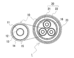
本例で使用する超電導ケーブルは、図1に示すように、3条の超電導ケーブルコア10を撚り合せて断熱管20の内部に収納した3心一括型の超電導ケーブル1である。
As shown in FIG. 1, the superconducting cable used in this example is a three-
超電導ケーブルコア10は、中心から順に、フォーマ11、超電導導体12、絶縁層13、外部導体層14、保護層15を備える。フォーマ11には、素線絶縁された複数本の銅素線を撚り合わせた撚り線構造のフォーマとした。超電導導体12および外部導体層14には、厚さ0.24mm、幅3.8mmのBi2223系Ag-Mnシーステープ線材を使用した。このテープ線材をフォーマ11上に多層に巻回して超電導導体12を形成し、超電導導体12の外周に厚さ125μm、幅20mmのPPLP(住友電気工業株式会社の登録商標)を多層に巻回して絶縁層13を形成した。さらに、絶縁層13の外周にシーステープ線材を多層に巻回して外部導体層14を形成した。その他、図示していないが、超電導導体12と絶縁層13との間に内部半導電層が、絶縁層13と外部導体層14との間に外部半導電層が形成される。
The
この超電導ケーブルコアの両端部(接続構造形成部)において、超電導導体の直上(内部半導電層を設ける場合、内部半導電層の直上)に絶縁層よりも誘電率εが高く、抵抗率ρが低い内部絶縁層を形成した。図2は、超電導ケーブルコア10の端部を拡大した部分断面図である。超電導ケーブルコア10の中間部(図2の中央の点線から右)は、フォーマ11、超電導導体12、絶縁層13、外部導体層14、保護層15の全てが、長手方向に亘って均等な厚さであるケーブル部10kである。一方、超電導ケーブルコア10の端部(図2の点線から左)は、超電導導体12の直上に内部絶縁層13aを設けた接続構造形成部10cである。接続構造形成部10cにおける内部絶縁層13a以外の層の厚さはケーブルコア10の長手方向に均一である。また、接続構造形成部10cにおける主絶縁層13bは、ケーブル部10kから連続的に形成された絶縁層13である。
At both ends of the superconducting cable core (connection structure forming portion), the dielectric constant ε is higher than the insulating layer and the resistivity ρ is directly above the superconducting conductor (if the internal semiconductive layer is provided, directly above the internal semiconductive layer). A low internal insulating layer was formed. FIG. 2 is a partial cross-sectional view in which the end of the
ここで、内部絶縁層13a、主絶縁層13bの誘電率εおよび抵抗率ρの関係は、以下に示す通りである。但し、AおよびBは定数である。
誘電率ε 抵抗率ρ(20℃)
内部絶縁層 約1.5A 約0.7BΩ・cm
主絶縁層 A BΩ・cm
Here, the relationship between the dielectric constant ε and the resistivity ρ of the inner insulating
Dielectric constant ε Resistivity ρ (20 ℃)
Internal insulation layer approx. 1.5A approx. 0.7BΩ · cm
Main insulation layer A BΩ · cm
内部絶縁層13aは、その厚さがケーブルコア10の端部に向かって徐々に厚くなるように巻回されたPPLPの層であり、主絶縁層13bを形成するPPLPとは誘電率εが異なる。具体的には、接続構造形成部10cの立ち上がり部分の位置にある内部絶縁層13aの厚さは、PPLP一枚分(約125μm)であり、接続構造形成部10cの端部における内部絶縁層13aの厚さは、PPLP五枚分(約625μm)である。なお、内部絶縁層13aの各部における厚さは、上記の厚さに限定されることはなく、接続部における電界の集中を緩和し、所望の裕度を確保することができるように適宜選択すれば良い。
The inner
超電導導体12の直上に誘電率εの高い内部絶縁層13aが形成されていることにより、電界強度の高い超電導導体12近傍での電界を緩和することができる。
Since the internal insulating
一方、超電導ケーブルコア10を収納する断熱管20は、内管21と外管22からなる二重管構造を有している(図1を参照)。また、内管21と外管22との間にスーパーインシュレーションなどの断熱材を配置した。内管21と上述したケーブルコア10とで囲まれた空間16が冷媒の流路になる。そして、断熱管20の端部に仕切りを形成して、内管21と外管22との間を封止し、両者の間を真空引きすることで断熱層を形成した。外管22の外周には防食層23が設けられている。
On the other hand, the
このような超電導ケーブルの端部にプーリングアイを取り付けて、このプーリングアイを牽引することで超電導ケーブルを管路に引き込む。図3は、プーリングアイ100を取り付けた超電導ケーブル1の端部を示す部分拡大図である。なお、図3では、2心のケーブルコアしか図示していないが、実際には3心存在する。
A pooling eye is attached to the end of such a superconducting cable, and the superconducting cable is pulled into the pipeline by pulling the pooling eye. FIG. 3 is a partially enlarged view showing an end portion of the
ケーブルコア10の端部、即ち、接続構造形成部10cは、内管21と外管22とからなる断熱管20の端部から突出させた状態とし、突出させた接続構造形成部10cの外周を覆うように補助管50を配置した。そして、補助管50の一端を外管22に固定し、他端をプーリングアイ100に取り付けた。プーリングアイ100を取り付けるにあたり、断熱管20の端部から突出した接続構造形成部10cの端部を段剥ぎし、露出された超電導導体12の端部にキャップCを被せて、超電導導体12を保護すると共に、超電導導体12がばらけないようにした。また、フォーマ11をプーリングアイ100のコア固定部101に固定した。このような構成により、ケーブルコア10を牽引するときの張力を、主として補助管50に連なる断熱管20とフォーマ11に分担させるようにした。
The end of the
プーリングアイ100が取り付けられる補助管50は、二重管構造である必要はないので、外管22の外径にほぼ一致した内径のものを使用した。この補助管50の内部の空間51は、断熱管20の内部の空間と比較して径方向に余裕があるので、内部絶縁層を巻き足して径の大きくなった接続構造形成部10cを補助管50内に収納することができた。従って、断熱管20の径(超電導ケーブル1の径)を大きくすることなく超電導ケーブル1を作製できた。
Since the
ここで、内部絶縁層13aの厚さをさらに厚くして、接続構造形成部10cの径を大きくした場合、各ケーブルコア10の撚りを絞めることにより補助管50内に収納することができる。このとき、ケーブルコアの撚りが絞まったとしても、ケーブル部10kで撚りの弛みを確保しているので、全体として十分なケーブルコアの撚りの弛みが確保されている。
Here, when the thickness of the inner insulating
次に、プーリングアイを牽引することで管路に引き込んだ超電導ケーブルを、他の導電部材と接続して、この接続部において補強絶縁構造を形成する。補強絶縁構造が形成される接続部としては、具体的には、一の超電導ケーブルと他の超電導ケーブルとを接続する中間接続部や、超電導ケーブルと他の電力機器とを接続する終端接続部が挙げられる。両接続部の構成は、基本的に、絶縁性のテープ状部材を巻回して補強絶縁層を形成する点、補強絶縁層の端部をペンシルダウン形状に形成する点で共通するため、ここでは、中間接続部のみを図4を参照して説明する。 Next, the superconducting cable drawn into the pipe line by pulling the pooling eye is connected to another conductive member, and a reinforcing insulating structure is formed at this connecting portion. Specifically, the connection part where the reinforced insulation structure is formed includes an intermediate connection part that connects one superconducting cable and another superconducting cable, and a terminal connection part that connects the superconducting cable and another power device. Can be mentioned. Since the configuration of both connecting portions is basically the same in that an insulating tape-like member is wound to form a reinforcing insulating layer, and the end of the reinforcing insulating layer is formed in a pencil down shape. Only the intermediate connection portion will be described with reference to FIG.
図4に示すように、中間接続部30は、二本の超電導ケーブルコアの端部を接続部材32を介して導通させ、この接続部材32の外周の近傍を補強絶縁層31で覆った構成である。
As shown in FIG. 4, the
この中間接続部30を形成するにあたり、まず初めに、ケーブルコアの端部(接続構造形成部の端部)を段剥ぎし、フォーマ11、超電導導体12、絶縁層13、外部導体層14を露出させた。フォーマ11と超電導導体12は、接続部材32を介して、他のフォーマ11と超電導導体12にそれぞれ接続される。絶縁層13の端部は、段剥ぎした部分で電界の集中を緩和するように、コアの端部側に向かって先細りのテーパ状であるペンシルダウン部13pを形成した。また、外部導体層14は、補強絶縁層31を形成できるように、ケーブル部10kと接続構造形成部10cの境界部分近傍まで超電導線材(シーステープ線材)の巻回を解いた状態とした。
In forming the
次に、接続部材32、超電導導体12および絶縁層13(主としてペンシルダウン部13p)の外周を覆うように補強絶縁層31を形成した。補強絶縁層31には、両端部に向かって先細りのテーパ状に形成したストレスコーン部31pが形成されている。ストレスコーン部31の立ち上がり部分sは、電界が集中し易く、絶縁の弱点となり易い。
Next, the reinforcing insulating
最後に、巻回を解いておいた外部導体層14が隣接するケーブル間で接続されるように、外部導体層14を補強絶縁層31の外周に延長して形成した。
Finally, the
以上、説明した中間接続部30では、超電導導体12の直上に高誘電率の内部絶縁層13aを設けることにより、電界強度の高い超電導導体12近傍での電界を緩和することができる。この部分ですでに電界を緩和していることにより、超電導導体12から比較的はなれた位置にあるストレスコーン部の立ち上がり部分sにおける電界強度も小さくすることができる。
As described above, in the intermediate connecting
さらに、内部絶縁層13aの抵抗率ρが主絶縁層13bの抵抗率ρと比較して小さいので、本例の超電導ケーブルにより直流送電を行なった場合、これら絶縁層13全体で電界を平滑化することができる。従って、中間接続部30における絶縁性能を向上させることができ、その結果、超電導ケーブル線路全体の信頼性を高めることができる。
Furthermore, since the resistivity ρ of the internal insulating
また、すでに述べたように絶縁層13は、テープ状線材を多層に巻回して形成しており、ケーブルコア10の布設現場で多層に巻回された絶縁層13(主絶縁層13b)を解くことは非常に困難である。しかし、本発明超電導ケーブルコア10によれば、予め超電導導体12の直上に内部絶縁層13aを設けているので、超電導ケーブル線路の布設時に絶縁層(主絶縁層13b)の巻回を解く必要をなくすることができる。
Further, as already described, the insulating
<実施例2>
本例では、実施例1の構成に加えて、外部導体層の直下に絶縁層よりも誘電率εが高く、抵抗率ρが高い絶縁性の層(外部絶縁層)を設けた超電導ケーブルコアを説明する。なお、超電導ケーブルコアに外部半導電層を設ける場合、外部半導電層の直下に外部絶縁層を設ける。本例の超電導ケーブルコアは、外部絶縁層を設ける以外は、実施例1の超電導ケーブルコアと同一の構成を有するため、相違点についてのみ説明する。
<Example 2>
In this example, in addition to the configuration of Example 1, a superconducting cable core having an insulating layer (external insulating layer) having a dielectric constant ε higher than an insulating layer and a high resistivity ρ immediately below the outer conductor layer is provided. explain. In the case where an external semiconductive layer is provided on the superconducting cable core, an external insulating layer is provided immediately below the external semiconductive layer. Since the superconducting cable core of this example has the same configuration as the superconducting cable core of Example 1 except that an external insulating layer is provided, only the differences will be described.
図5は、本例の超電導ケーブルコアを用いた中間接続部を示す部分断面図である。図5に示すように、この超電導ケーブルコア10の主絶縁層13bと外部導体層14との間には、外部絶縁層13cが設けられている。外部絶縁層13cは、内部絶縁層13aと同様に、ケーブル部10kと接続構造形成部10cとの境界部分からケーブルコア10の端部に向かって徐々に厚くなるように形成されている。外部絶縁層13cをケーブルコアの端部に向かって厚くなるように形成するには、PPLP(登録商標)を巻回するときの重ね代を調節することで容易に行なうことができる。
FIG. 5 is a partial cross-sectional view showing an intermediate connection portion using the superconducting cable core of this example. As shown in FIG. 5, an external insulating
上述した各絶縁層13a〜13cの誘電率εと抵抗率ρを以下に示す。但し、AおよびBは定数である。
誘電率ε 抵抗率ρ(20℃)
内部絶縁層 約1.5A 約0.8BΩ・cm
主絶縁層 A BΩ・cm
外部絶縁層 約1.5A 約1.2BΩ・cm
The dielectric constant ε and resistivity ρ of each of the insulating
Dielectric constant ε Resistivity ρ (20 ℃)
Internal insulation layer About 1.5A About 0.8BΩ · cm
Main insulation layer A BΩ · cm
External insulation layer approx. 1.5A approx. 1.2BΩ · cm
上記のように、誘電率εは、超電導導体12から外部導体層14に向かって、高→中→高となっている。従って、内部絶縁層13aの位置に加えて、外部絶縁層13cの位置でも電界を緩和できる。また、外部絶縁層13cが存在することにより、極性が反転した場合、即ち、外部導体層14から超電導導体12に向かって電界が形成された場合でも、効果的に電界を緩和することができる。
As described above, the dielectric constant ε is high → medium → high from the
一方、抵抗率ρは、超電導導体12から外部導体層14に向かって低→中→高となっている。従って、本例の超電導ケーブル線路により直流送電を行なった場合、直流電界分布を絶縁層の厚さ方向に平滑化することができる。また、仮に、負極性の雷インパルスもしくは開閉インパルスがケーブル線路に印加され、絶縁層の外周に設けられる外部導体層14の直下の位置が最大電界強度となった場合でも、抵抗率ρの高い外部絶縁層13cにより最大電界強度に耐えることができる。
On the other hand, the resistivity ρ is low → medium → high from the
<変形例2−1>
本例では、実施例2の構成のうち、外部絶縁層の厚さを変化させた超電導ケーブル線路を説明する。この線路では、超電導ケーブルコアの外部絶縁層の構成が異なる以外、実施例2と同様であるため、図6を参照して相違点についてのみ説明する。
<Modification 2-1>
In this example, a superconducting cable line in which the thickness of the external insulating layer is changed in the configuration of Example 2 will be described. Since this line is the same as that of Example 2 except that the configuration of the external insulating layer of the superconducting cable core is different, only the differences will be described with reference to FIG.
図6は、本例の超電導ケーブル(コア)を用いた中間接続部の近傍を示す部分断面図である。図に示すように、本例の外部絶縁層13cは、超電導ケーブルコア10の端部からケーブル部10kに向かって徐々に厚く形成され、ストレスコーン部31pの立ち上がり部分sの位置で最大の厚さとなっている。そして、立ち上がり部分sから接続構造形成部10cとケーブル部10kとの境界部分に向かって徐々に薄くなっている。ここで、外部絶縁層13cは、ストレスコーン部31pにおいて、段差が生じないように形成すると良い。
FIG. 6 is a partial cross-sectional view showing the vicinity of an intermediate connection portion using the superconducting cable (core) of this example. As shown in the figure, the outer insulating
上記構成となすことにより、補強絶縁層31のうち、特に電界が集中し易いストレスコーンの立ち上がり部分sにおいて、効果的に電界を緩和することができる。従って、より信頼性の高い接続部を形成することができる。
With the above configuration, the electric field can be effectively relaxed in the rising portion s of the stress cone where the electric field tends to concentrate in the reinforcing insulating
本発明超電導ケーブルコアを備える超電導ケーブルは、既設の管路に布設可能なので、信頼性の高い超電導ケーブル線路に好適に利用可能である。また、本発明超電導ケーブル線路は、AC、DCの両方に好適に利用可能である。 Since the superconducting cable provided with the superconducting cable core of the present invention can be installed in an existing pipe line, it can be suitably used for a highly reliable superconducting cable line. The superconducting cable line of the present invention can be suitably used for both AC and DC.
1 超電導ケーブル
10 超電導ケーブルコア 10k ケーブル部 10c 接続構造形成部
11 フォーマ 12 超電導導体 13 絶縁層 14 外部導体層 15 防食層
20 断熱管 21 断熱内管 22 断熱外管 23 保護層
50 補助管 51 空間
100 プーリングアイ 101 コア固定部
30 中間接続部 31 補強絶縁層 31p ストレスコーン部 32 接続部材
13p ペンシルダウン部 13a 内部絶縁層 13b 主絶縁層 13c 外部絶縁層
1 Superconducting cable
10
11 Former 12
20
50
100
30
13p Pencil down
Claims (7)
超電導ケーブルコアは、長手方向にケーブル部と、ケーブル部の両端部に位置して、他の導電部材と接続したときに補強絶縁構造が形成される接続構造形成部とに区分され、
接続構造形成部は、超電導ケーブルコアのうち、少なくとも超電導ケーブルコアの端部から補強絶縁構造の端部までの範囲であり、
接続構造形成部における絶縁層の絶縁性能を、ケーブル部における絶縁層の絶縁性能よりも高くしたことを特徴とする超電導ケーブルコア。 A superconducting cable core comprising a superconducting conductor and an insulating layer covering the outer periphery of the superconducting conductor,
The superconducting cable core is divided into a cable part in the longitudinal direction, and a connection structure forming part that is located at both ends of the cable part and in which a reinforcing insulating structure is formed when connected to another conductive member,
The connection structure forming portion is a range from at least the end portion of the superconducting cable core to the end portion of the reinforcing insulating structure among the superconducting cable cores,
A superconducting cable core characterized in that the insulating performance of the insulating layer in the connection structure forming portion is higher than the insulating performance of the insulating layer in the cable portion.
内部絶縁層の誘電率が、主絶縁層の誘電率よりも高いことを特徴とする請求項1に記載の超電導ケーブルコア。 The insulating layer in the connection structure forming portion includes a main insulating layer and an internal insulating layer disposed between the main insulating layer and the superconducting conductor,
The superconducting cable core according to claim 1, wherein the dielectric constant of the inner insulating layer is higher than the dielectric constant of the main insulating layer.
超電導ケーブルコアの外周に配置される二重管構造からなる断熱層とを有し、
この二重管の端部から接続構造形成部が突出するように構成したことを特徴とする超電導ケーブル。 The superconducting cable core according to any one of claims 1 to 5,
A heat insulating layer having a double-pipe structure disposed on the outer periphery of the superconducting cable core;
A superconducting cable characterized in that a connection structure forming portion protrudes from an end portion of the double pipe.
この超電導ケーブル線路は、直流超電導ケーブル線路または交流超電導ケーブル線路のいずれかであることを特徴とする超電導ケーブル線路。 A superconducting cable line laid using the superconducting cable according to claim 6,
The superconducting cable line is either a DC superconducting cable line or an AC superconducting cable line.
Priority Applications (8)
| Application Number | Priority Date | Filing Date | Title |
|---|---|---|---|
| JP2006111032A JP2007287388A (en) | 2006-04-13 | 2006-04-13 | Superconductive cable core, and superconductive cable |
| EP07740884A EP2006862B1 (en) | 2006-04-13 | 2007-04-03 | Superconducting cable core and superconducting cable |
| PCT/JP2007/057448 WO2007119655A1 (en) | 2006-04-13 | 2007-04-03 | Superconducting cable core and superconducting cable |
| US11/917,581 US7800000B2 (en) | 2006-04-13 | 2007-04-03 | Superconducting-cable core and superconducting cable |
| CN2007800006580A CN101331560B (en) | 2006-04-13 | 2007-04-03 | Superconducting cable core and superconducting cable |
| KR1020077030548A KR101306519B1 (en) | 2006-04-13 | 2007-04-03 | Superconducting cable core and superconducting cable |
| CA002609321A CA2609321A1 (en) | 2006-04-13 | 2007-04-03 | Superconducting cable core and superconducting cable |
| TW096112796A TW200802419A (en) | 2006-04-13 | 2007-04-12 | Super conductive cable and its cable core |
Applications Claiming Priority (1)
| Application Number | Priority Date | Filing Date | Title |
|---|---|---|---|
| JP2006111032A JP2007287388A (en) | 2006-04-13 | 2006-04-13 | Superconductive cable core, and superconductive cable |
Publications (1)
| Publication Number | Publication Date |
|---|---|
| JP2007287388A true JP2007287388A (en) | 2007-11-01 |
Family
ID=38609419
Family Applications (1)
| Application Number | Title | Priority Date | Filing Date |
|---|---|---|---|
| JP2006111032A Pending JP2007287388A (en) | 2006-04-13 | 2006-04-13 | Superconductive cable core, and superconductive cable |
Country Status (8)
| Country | Link |
|---|---|
| US (1) | US7800000B2 (en) |
| EP (1) | EP2006862B1 (en) |
| JP (1) | JP2007287388A (en) |
| KR (1) | KR101306519B1 (en) |
| CN (1) | CN101331560B (en) |
| CA (1) | CA2609321A1 (en) |
| TW (1) | TW200802419A (en) |
| WO (1) | WO2007119655A1 (en) |
Cited By (3)
| Publication number | Priority date | Publication date | Assignee | Title |
|---|---|---|---|---|
| JP2009216930A (en) * | 2008-03-10 | 2009-09-24 | Ricoh Co Ltd | Image forming apparatus and image density control method |
| JP2010186733A (en) * | 2009-01-15 | 2010-08-26 | Sumitomo Electric Ind Ltd | Connecting part of superconducting cable, and superconducting cable line using it |
| WO2013105364A1 (en) | 2012-01-10 | 2013-07-18 | 住友電気工業株式会社 | Connecting structure for room-temperature insulation type superconductive cable |
Families Citing this family (10)
| Publication number | Priority date | Publication date | Assignee | Title |
|---|---|---|---|---|
| JP5731564B2 (en) * | 2013-03-29 | 2015-06-10 | 昭和電線ケーブルシステム株式会社 | Superconducting cable terminal structure |
| FR3010847B1 (en) * | 2013-09-19 | 2017-12-29 | Nexans | JUNCTION OF SUPERCONDUCTING CABLES |
| KR102351517B1 (en) * | 2015-02-17 | 2022-01-14 | 엘에스전선 주식회사 | Installation device for cable |
| KR101858899B1 (en) | 2017-02-16 | 2018-05-16 | 엘에스전선 주식회사 | Power cable |
| KR101998944B1 (en) * | 2017-03-24 | 2019-07-11 | 엘에스전선 주식회사 | Power cable |
| CN108899157B (en) * | 2018-08-17 | 2024-02-13 | 广东电网有限责任公司 | Superconducting coil of current limiter with spiral structure |
| CN109741900A (en) * | 2019-01-31 | 2019-05-10 | 中国科学院合肥物质科学研究院 | The sub- cable docking superconducting joint of Bi-2212 armored cable and manufacturing method |
| CN211507914U (en) * | 2020-04-01 | 2020-09-15 | 吉林省中赢高科技有限公司 | Novel tip aluminium part |
| WO2021262319A2 (en) * | 2020-05-07 | 2021-12-30 | Massachusetts Institute Of Technology | Cabling method of superconducting flat wires |
| CN113419100A (en) * | 2021-06-21 | 2021-09-21 | 国网上海市电力公司 | Method for testing current distribution of each layer of superconducting cable |
Family Cites Families (11)
| Publication number | Priority date | Publication date | Assignee | Title |
|---|---|---|---|---|
| US6342672B1 (en) * | 1994-02-14 | 2002-01-29 | Canon Kabushiki Kaisha | Superconducting lead with recoverable and nonrecoverable insulation |
| JP3239036B2 (en) * | 1994-02-14 | 2001-12-17 | キヤノン株式会社 | Superconducting device |
| JP3547222B2 (en) * | 1995-08-11 | 2004-07-28 | 古河電気工業株式会社 | Multi-layer superconducting cable |
| US6596945B1 (en) * | 1998-09-11 | 2003-07-22 | Southwire Company | Superconducting cable |
| MXPA02007435A (en) * | 2002-08-01 | 2004-07-16 | Servicios Condumex Sa | Energy superconducting cable with improved superconducting core. |
| JP2005012915A (en) * | 2003-06-19 | 2005-01-13 | Sumitomo Electric Ind Ltd | Connection structure of superconductive cable and insulated spacer for connecting superconductive cable |
| JP4300517B2 (en) | 2003-09-24 | 2009-07-22 | 住友電気工業株式会社 | Superconducting cable |
| JP4593933B2 (en) * | 2004-01-22 | 2010-12-08 | 住友電気工業株式会社 | Connection structure of multiphase superconducting cable |
| JP2006059695A (en) | 2004-08-20 | 2006-03-02 | Sumitomo Electric Ind Ltd | Superconductive cable |
| JP4716160B2 (en) | 2004-10-14 | 2011-07-06 | 住友電気工業株式会社 | Superconducting cable |
| US7943852B2 (en) * | 2005-03-14 | 2011-05-17 | Sumitomo Electric Industries, Ltd. | Superconducting cable |
-
2006
- 2006-04-13 JP JP2006111032A patent/JP2007287388A/en active Pending
-
2007
- 2007-04-03 KR KR1020077030548A patent/KR101306519B1/en not_active IP Right Cessation
- 2007-04-03 US US11/917,581 patent/US7800000B2/en not_active Expired - Fee Related
- 2007-04-03 EP EP07740884A patent/EP2006862B1/en not_active Expired - Fee Related
- 2007-04-03 WO PCT/JP2007/057448 patent/WO2007119655A1/en active Application Filing
- 2007-04-03 CN CN2007800006580A patent/CN101331560B/en not_active Expired - Fee Related
- 2007-04-03 CA CA002609321A patent/CA2609321A1/en not_active Abandoned
- 2007-04-12 TW TW096112796A patent/TW200802419A/en unknown
Cited By (3)
| Publication number | Priority date | Publication date | Assignee | Title |
|---|---|---|---|---|
| JP2009216930A (en) * | 2008-03-10 | 2009-09-24 | Ricoh Co Ltd | Image forming apparatus and image density control method |
| JP2010186733A (en) * | 2009-01-15 | 2010-08-26 | Sumitomo Electric Ind Ltd | Connecting part of superconducting cable, and superconducting cable line using it |
| WO2013105364A1 (en) | 2012-01-10 | 2013-07-18 | 住友電気工業株式会社 | Connecting structure for room-temperature insulation type superconductive cable |
Also Published As
| Publication number | Publication date |
|---|---|
| KR101306519B1 (en) | 2013-09-09 |
| TW200802419A (en) | 2008-01-01 |
| KR20080108383A (en) | 2008-12-15 |
| CN101331560A (en) | 2008-12-24 |
| EP2006862A1 (en) | 2008-12-24 |
| US20090082210A1 (en) | 2009-03-26 |
| WO2007119655A1 (en) | 2007-10-25 |
| CN101331560B (en) | 2010-12-01 |
| CA2609321A1 (en) | 2007-10-25 |
| EP2006862B1 (en) | 2013-01-30 |
| EP2006862A4 (en) | 2012-04-04 |
| US7800000B2 (en) | 2010-09-21 |
Similar Documents
| Publication | Publication Date | Title |
|---|---|---|
| JP2007287388A (en) | Superconductive cable core, and superconductive cable | |
| US7498519B2 (en) | Joint for superconducting cable | |
| US7238887B2 (en) | DC superconducting cable | |
| JPWO2013157513A1 (en) | Superconducting cable connection structure | |
| JP4399763B2 (en) | DC superconducting cable line | |
| JPWO2011152342A1 (en) | Terminal structure of superconducting cable conductor | |
| KR101148574B1 (en) | Superconducting cable | |
| JP4843937B2 (en) | Superconducting cable | |
| JP5390297B2 (en) | Superconducting cable connection and superconducting cable line using the same | |
| JP2006059695A (en) | Superconductive cable | |
| WO2006041070A1 (en) | Superconducting cable connection structure | |
| JP4720976B2 (en) | Superconducting cable | |
| WO2006061960A1 (en) | Dc superconductive cable design system | |
| JP4986291B2 (en) | Superconducting cable | |
| JP2010020970A (en) | Connecting structure of superconductive cable core | |
| JP3877057B2 (en) | High temperature superconducting cable | |
| JP5273572B2 (en) | Laying the superconducting cable | |
| JP4716160B2 (en) | Superconducting cable | |
| JP2006320115A (en) | Connecting part of superconductive cable | |
| JP5910996B2 (en) | Superconducting cable and method of manufacturing superconducting cable | |
| JP2012174403A (en) | Normal temperature insulating type superconducting cable and method for manufacturing the same | |
| JP6169125B2 (en) | Cable laying structure and cable laying method | |
| JP2009076401A (en) | Superconductive cable | |
| JP5830498B2 (en) | Superconducting cable connection structure | |
| JP4544433B2 (en) | Intermediate connection of superconducting cable |