JP2007266579A - Light emitting device - Google Patents
Light emitting device Download PDFInfo
- Publication number
- JP2007266579A JP2007266579A JP2007019580A JP2007019580A JP2007266579A JP 2007266579 A JP2007266579 A JP 2007266579A JP 2007019580 A JP2007019580 A JP 2007019580A JP 2007019580 A JP2007019580 A JP 2007019580A JP 2007266579 A JP2007266579 A JP 2007266579A
- Authority
- JP
- Japan
- Prior art keywords
- phosphor
- wavelength
- light
- emission
- light emitting
- Prior art date
- Legal status (The legal status is an assumption and is not a legal conclusion. Google has not performed a legal analysis and makes no representation as to the accuracy of the status listed.)
- Pending
Links
Images


Classifications
-
- H—ELECTRICITY
- H01—ELECTRIC ELEMENTS
- H01L—SEMICONDUCTOR DEVICES NOT COVERED BY CLASS H10
- H01L2224/00—Indexing scheme for arrangements for connecting or disconnecting semiconductor or solid-state bodies and methods related thereto as covered by H01L24/00
- H01L2224/01—Means for bonding being attached to, or being formed on, the surface to be connected, e.g. chip-to-package, die-attach, "first-level" interconnects; Manufacturing methods related thereto
- H01L2224/42—Wire connectors; Manufacturing methods related thereto
- H01L2224/44—Structure, shape, material or disposition of the wire connectors prior to the connecting process
- H01L2224/45—Structure, shape, material or disposition of the wire connectors prior to the connecting process of an individual wire connector
- H01L2224/45001—Core members of the connector
- H01L2224/45099—Material
- H01L2224/451—Material with a principal constituent of the material being a metal or a metalloid, e.g. boron (B), silicon (Si), germanium (Ge), arsenic (As), antimony (Sb), tellurium (Te) and polonium (Po), and alloys thereof
- H01L2224/45138—Material with a principal constituent of the material being a metal or a metalloid, e.g. boron (B), silicon (Si), germanium (Ge), arsenic (As), antimony (Sb), tellurium (Te) and polonium (Po), and alloys thereof the principal constituent melting at a temperature of greater than or equal to 950°C and less than 1550°C
- H01L2224/45144—Gold (Au) as principal constituent
-
- H—ELECTRICITY
- H01—ELECTRIC ELEMENTS
- H01L—SEMICONDUCTOR DEVICES NOT COVERED BY CLASS H10
- H01L2224/00—Indexing scheme for arrangements for connecting or disconnecting semiconductor or solid-state bodies and methods related thereto as covered by H01L24/00
- H01L2224/01—Means for bonding being attached to, or being formed on, the surface to be connected, e.g. chip-to-package, die-attach, "first-level" interconnects; Manufacturing methods related thereto
- H01L2224/42—Wire connectors; Manufacturing methods related thereto
- H01L2224/47—Structure, shape, material or disposition of the wire connectors after the connecting process
- H01L2224/48—Structure, shape, material or disposition of the wire connectors after the connecting process of an individual wire connector
- H01L2224/4805—Shape
- H01L2224/4809—Loop shape
- H01L2224/48091—Arched
-
- H—ELECTRICITY
- H01—ELECTRIC ELEMENTS
- H01L—SEMICONDUCTOR DEVICES NOT COVERED BY CLASS H10
- H01L2224/00—Indexing scheme for arrangements for connecting or disconnecting semiconductor or solid-state bodies and methods related thereto as covered by H01L24/00
- H01L2224/73—Means for bonding being of different types provided for in two or more of groups H01L2224/10, H01L2224/18, H01L2224/26, H01L2224/34, H01L2224/42, H01L2224/50, H01L2224/63, H01L2224/71
- H01L2224/732—Location after the connecting process
- H01L2224/73251—Location after the connecting process on different surfaces
- H01L2224/73265—Layer and wire connectors
Abstract
Description
本発明は、発光ダイオードランプなどの発光装置に関する。 The present invention relates to a light emitting device such as a light emitting diode lamp.
発光ダイオード(LED:Light Emitting Diode)を用いたLEDランプは、液晶ディスプレイ、携帯電話、情報端末などのバックライト、屋内外広告など、多方面への展開が飛躍的に進んでいる。さらに、LEDランプは、長寿命で信頼性が高く、また低消費電力、耐衝撃性、高純度表示色、軽薄短小化の実現などの特徴を有することから、産業用途のみならず一般照明用途への適用も試みられている。このようなLEDランプを種々の用途に適用する場合、白色発光を得ることが重要となる。 LED lamps using light emitting diodes (LEDs) are rapidly expanding in various fields such as backlights for liquid crystal displays, mobile phones, information terminals, and indoor / outdoor advertisements. In addition, LED lamps have features such as long life and high reliability, and low power consumption, impact resistance, high purity display color, lightness, thinness, and other features. Application of is also being attempted. When such an LED lamp is applied to various uses, it is important to obtain white light emission.
LEDランプで白色発光を実現する代表的な方式としては、(1)青、緑および赤の各色に発光する3つのLEDチップを使用する方式、(2)青色発光のLEDチップと黄色ないし橙色発光の蛍光体とを組合せる方式、(3)紫外線発光のLEDチップと青色、緑色および赤色発光の三色混合蛍光体とを組合せる方式、の3つが挙げられる。これらのうち、一般的には(2)の方式が広く実用化されている。 Typical methods for realizing white light emission with an LED lamp are (1) a method using three LED chips that emit light in blue, green and red colors, and (2) a blue light emitting LED chip and yellow or orange light emission. And (3) a method of combining an ultraviolet light emitting LED chip and a blue, green and red light emitting three-color mixed phosphor. Of these, the method (2) is generally widely used.
そして、上記した(2)の方式を適用したLEDランプの構造としては、LEDチップを装備したカップ型のフレーム内に蛍光体を混合した透明樹脂を流し込み、これを固化させて蛍光体を含有する樹脂層を形成した構造が一般的である(例えば、特許文献1参照)。 And as a structure of the LED lamp to which the above-mentioned method (2) is applied, a transparent resin mixed with a phosphor is poured into a cup-shaped frame equipped with an LED chip, and this is solidified to contain the phosphor. A structure in which a resin layer is formed is common (see, for example, Patent Document 1).
近年、このようなLEDランプにおいて、演色性と呼ばれる色の見え方が重視されている。演色性は、自然光に近い照明を基準光にして光源による色の見え方を評価したものであり、JISに定められている試験色を、試料光源と基準光でそれぞれ照明したときの色ずれの大きさを数値化したものが演色評価数である。基準光で見たときを100とし、色ずれが大きくなるにしたがって数値が小さくなる。 In recent years, in such LED lamps, emphasis is placed on the color appearance called color rendering properties. Color rendering is an evaluation of the color appearance of a light source using illumination close to natural light as the reference light, and the color shift when the test color specified in JIS is illuminated with the sample light source and the reference light, respectively. The numerical value of the size is the color rendering index. The value when viewed with reference light is set to 100, and the numerical value decreases as the color shift increases.
演色評価数には、平均演色評価数Raと特殊演色評価数Riがあり、平均演色評価数Raは、試験No.1〜8の演色評価数値の平均値として表される。これらの演色評価数は、その照明の基準光との色ずれの方向が好ましい方向にあるかどうかに関係なく数値化されているので、演色評価数が低くても好ましい色に見える場合がある。 The color rendering index includes an average color rendering index Ra and a special color rendering index Ri. It is expressed as an average value of 1 to 8 color rendering evaluation values. Since these color rendering evaluation numbers are quantified regardless of whether the direction of the color shift from the reference light of the illumination is in a preferable direction, there may be a case where a preferable color appears even if the color rendering evaluation number is low.
現在主流となっている白色LEDは、青色発光のLEDチップと黄色ないし橙色発光の蛍光体とを組合せる方式であり、この方式のLEDでは、赤み成分が不足しているため演色性が十分ではなかった。そのため、黄色ないし橙色発光の蛍光体に加えて、窒化物系や硫化物系などの赤色発光の蛍光体を配合することにより、演色性を向上させることが行われている。 White LEDs, which are currently in the mainstream, are a combination of a blue light emitting LED chip and a yellow or orange light emitting phosphor. This type of LED has insufficient redness, so that color rendering is not sufficient. There wasn't. For this reason, in addition to yellow or orange light emitting phosphors, color rendering properties are improved by blending red light emitting phosphors such as nitrides and sulfides.
しかしながら、赤色蛍光体の添加により特殊演色評価数R9の値が増大し、それにしたがって平均演色評価数Raが増大するが、光源色が赤みを帯びるため、必ずしも色の見え方が好ましいわけではなかった。 However, the addition of the red phosphor increases the value of the special color rendering index R9, and the average color rendering index Ra increases accordingly. However, since the light source color is reddish, the color appearance is not always preferable. .
また、赤色蛍光体が窒化物系などの場合には、LEDチップからの波長460nmの青色発光だけでなく、黄色系蛍光体から発光される緑色光から黄色光間の光をも吸収して励起に使用するため、赤色発光の蛍光体を使用すると、LEDランプの発光効率が大幅に下がるという問題があった。
本発明はこのような問題を解決するためになされたもので、赤色発光の蛍光体を用いることによる発光効率の低下をできるだけ抑制し、高い演色性を維持しつつ発光効率を向上させることが可能な発光装置を提供することを目的としている。 The present invention has been made to solve such a problem, and it is possible to suppress a decrease in luminous efficiency due to the use of a phosphor emitting red light as much as possible, and to improve luminous efficiency while maintaining high color rendering properties. An object of the present invention is to provide a simple light emitting device.
請求項1記載の発光装置は、青色光を放射する発光素子と;前記発光素子から放射された青色光により励起されて、波長490〜510nmと530〜580nmおよび610〜660nmにそれぞれピークを有する光を発光する蛍光体を含有する蛍光体層と;を具備することを特徴としている。
The light-emitting device according to
請求項2記載の発光装置は、請求項1記載の発光装置において、前記蛍光体の発光スペクトルにおける波長490〜510nmの発光ピークの発光強度をA、波長530〜580nmの発光ピークの発光強度をB、波長610〜660nmの発光ピークの発光強度をCとするとき、BとAの比(B/A)が0.8〜1.2であり、かつCとAの比(C/A)が0.5〜1.2であることを特徴としている。
The light emitting device according to
請求項3記載の発光装置は、請求項1または2記載の発光装置において、前記蛍光体が、波長490〜510nmと波長530〜580nmにそれぞれ発光ピークを有する第1の蛍光体と、波長610〜660nmに発光ピークを有する第2の蛍光体をそれぞれ含有することを特徴としている。
The light emitting device according to
請求項4記載の発光装置は、請求項3記載の発光装置において、前記蛍光体が、波長530〜580nmに発光のピークを有する第3の蛍光体をさらに含有することを特徴としている。
The light-emitting device according to
請求項5記載の発光装置は、青色光を放射する青色発光素子と;前記青色発光素子から放射された青色光により励起されて、波長490〜510nmと530〜580nmおよび610〜660nmにそれぞれ発光ピークを有するとともに、前記青色光との混色により、波長470〜490nmに発光強度の谷部を有し、かつ前記青色光の発光ピークの発光強度に対する前記谷部の発光強度の割合が0.7〜0.9である可視光を発する蛍光体を含有する蛍光体層と;を具備することを特徴としている。
The light-emitting device according to
請求項6記載の発光装置は、請求項5記載の発光装置において、前記蛍光体の発光スペクトルにおける波長490〜510nmの発光ピークの発光強度をA、波長530〜580nmの発光ピークの発光強度をB、波長610〜660nmの発光ピークの発光強度をCとするとき、BとAの比(B/A)が0.8〜1.2であり、かつCとAの比(C/A)が0.5〜1.2であることを特徴としている。
The light emitting device according to
請求項7記載の発光装置は、請求項5または6記載の発光装置において、前記蛍光体が、波長490〜510nmと波長530〜580nmにそれぞれ発光ピークを有する第1の蛍光体と、波長610〜660nmに発光ピークを有する第2の蛍光体をそれぞれ含有することを特徴としている。
The light-emitting device according to
請求項8記載の発光装置は、請求項7記載の発光装置において、前記蛍光体が、波長530〜580nmに発光のピークを有する第3の蛍光体をさらに含有することを特徴としている。
The light-emitting device according to
請求項9記載の発光装置は、請求項7または8記載の発光装置において、前記蛍光体の波長490〜510nmの発光ピークの半値幅は125〜145nmであり、波長530〜580nmの発光ピークの半値幅は90〜110nmであり、波長610〜660nmの発光ピークの半値幅は80〜100nmであることを特徴としている。
The light-emitting device according to claim 9 is the light-emitting device according to
上記した請求項1ないし請求項9記載の発明において、用語の定義および技術的意味は、特に指定しない限り以下の通りである。
In the above-described inventions according to
青色光を放射する発光素子は、主波長が420〜480nm(例えば460nm)の青色光を放射し、放射した青色光により蛍光体を励起して可視光を発光させるものである。本発明で用いられる青色光を放射する発光素子としては、例えば、青色発光タイプのLEDチップなどが挙げられるが、これに限定されるものではない。 A light emitting element that emits blue light emits blue light having a dominant wavelength of 420 to 480 nm (for example, 460 nm), and excites a phosphor with the emitted blue light to emit visible light. Examples of the light emitting element that emits blue light used in the present invention include, but are not limited to, a blue light emitting type LED chip.
蛍光体は、このような発光素子から放射された青色光により励起されて可視光を発光し、この可視光と発光素子から放射される青色光との混色によって、発光装置として所望の発光色を得るものである。 The phosphor is excited by blue light emitted from such a light emitting element to emit visible light, and a desired emission color as a light emitting device is obtained by mixing the visible light and the blue light emitted from the light emitting element. To get.
本発明において蛍光体としては、波長490〜510nmの範囲と波長530〜580nmの範囲にそれぞれ発光強度のピーク(以下、発光ピークと示す。)を有する第1の蛍光体と、波長610〜660nmの範囲に発光ピークを有する第2の蛍光体との計2種類の蛍光体を混合して使用することができる。また、波長490〜510nmと波長530〜580nmにそれぞれ発光ピークを有する第1の蛍光体と、波長610〜660nmに発光ピークを有する第2の蛍光体とともに、波長530〜580nmに発光ピークを有する第3の蛍光体を含有させることができる。さらに、各波長範囲にそれぞれ1つの発光ピークを有する3種類の蛍光体を混合して使用してもよい。すなわち、主波長(ピーク波長)が490〜510nmの第1の蛍光体と、主波長が530〜580nmの第2の蛍光体、および主波長が610〜660nmの第3の蛍光体を混合した蛍光体を使用することができる。これら2種類または3種類の蛍光体の配合割合は、発光装置からの発光の平均演色評価数Raが高く、かつ高い発光効率が得られるように調整される。 In the present invention, the phosphor includes a first phosphor having emission intensity peaks (hereinafter referred to as emission peaks) in a wavelength range of 490 to 510 nm and a wavelength range of 530 to 580 nm, and a wavelength of 610 to 660 nm. A total of two types of phosphors, the second phosphor having an emission peak in the range, can be used. A first phosphor having an emission peak at wavelengths of 490 to 510 nm and a second phosphor having an emission peak at wavelengths of 610 to 660 nm together with a first phosphor having an emission peak at wavelengths of 490 to 510 nm and a wavelength of 530 to 580 nm. 3 phosphors can be contained. Further, three types of phosphors each having one emission peak in each wavelength range may be mixed and used. That is, fluorescence in which a first phosphor having a dominant wavelength (peak wavelength) of 490 to 510 nm, a second phosphor having a dominant wavelength of 530 to 580 nm, and a third phosphor having a dominant wavelength of 610 to 660 nm are mixed. The body can be used. The blending ratio of these two or three kinds of phosphors is adjusted so that the average color rendering index Ra of light emission from the light emitting device is high and high light emission efficiency is obtained.
前記2種類または3種類の蛍光体を混合した蛍光体(蛍光体混合物)において、発光スペクトルにおける波長490〜510nmの範囲の発光ピークの強度(発光強度)をA、波長530〜580nmの範囲の発光ピークの強度をB、波長610〜660nmの範囲の発光ピークの強度をCとするとき、BとAの比(B/A)が0.8〜1.2であり、かつCとAの比(C/A)が0.5〜1.2であることが好ましい。 In the phosphor (phosphor mixture) in which the two or three kinds of phosphors are mixed, the emission peak intensity (emission intensity) in the wavelength range of 490 to 510 nm in the emission spectrum is A, and the emission is in the wavelength range of 530 to 580 nm. When the intensity of the peak is B and the intensity of the emission peak in the wavelength range of 610 to 660 nm is C, the ratio of B to A (B / A) is 0.8 to 1.2, and the ratio of C to A (C / A) is preferably 0.5 to 1.2.
本発明の蛍光体において、波長490〜510nmの発光ピークは125〜145nmの半値幅を有し、波長530〜580nmの発光ピークは90〜110nmの半値幅を有することが好ましい。同様に、波長610〜660nmの発光ピークは80〜100nmの半値幅を有することが好ましい。なお、蛍光体の発光ピークにおける半値幅は、発光ピークの強度の1/2の強度におけるスペクトルの広がり幅(波長)をいう。 In the phosphor of the present invention, the emission peak at a wavelength of 490 to 510 nm preferably has a half width of 125 to 145 nm, and the emission peak of a wavelength of 530 to 580 nm preferably has a half width of 90 to 110 nm. Similarly, the emission peak at a wavelength of 610 to 660 nm preferably has a half width of 80 to 100 nm. Note that the half-width at the emission peak of the phosphor refers to the spread width (wavelength) of the spectrum at half the intensity of the emission peak.
また本発明では、前記した2種類または3種類の蛍光体を使用することで、青色発光素子から放射された青色光との混色により、波長470〜490nmに発光強度の谷部を有し、この谷部の発光強度(Dとする。)の青色光の発光ピークの強度(Eとする。)に対する割合(D/E)が0.7〜0.9になるような光が発せられるように構成することができる。 Further, in the present invention, by using the above-described two or three kinds of phosphors, there is a valley portion of emission intensity at a wavelength of 470 to 490 nm due to color mixture with blue light emitted from the blue light emitting element. Light is emitted so that the ratio (D / E) of the emission intensity of the valley (denoted as D) to the intensity of the emission peak of blue light (denoted as E) is 0.7 to 0.9. Can be configured.
蛍光体を含む蛍光体層は、前記2種類または3種類の蛍光体を、シリコーン樹脂やエポキシ樹脂のような透明樹脂に加えて混合・分散させた層として形成される。発光素子の外側を覆うように形成することができるが、発光素子を直接覆うようにして透明樹脂層を形成し、その上に前記した2種類または3種類の蛍光体を含む層を設けることも可能である。 The phosphor layer containing the phosphor is formed as a layer obtained by mixing and dispersing the two or three kinds of phosphors in addition to a transparent resin such as a silicone resin or an epoxy resin. Although it can be formed so as to cover the outside of the light emitting element, a transparent resin layer is formed so as to directly cover the light emitting element, and a layer containing the two or three kinds of phosphors described above may be provided thereon. Is possible.
請求項1および3記載の発光装置によれば、蛍光体からの発光スペクトルが、波長530〜580nmの範囲の発光ピークと波長610〜660nmの範囲の発光ピークとともに、波長490〜510nmの範囲にも発光ピークを有しているので、高演色性の発光を得ることができる。また、主波長が610〜660nmの赤色蛍光体の配合量を低減しても高い演色性を得ることができ、かつ赤色蛍光体の減量により発光効率の向上を達成することができる。
According to the light emitting device of
請求項2記載の発光装置によれば、蛍光体の発光スペクトルにおける各波長範囲の発光ピークの強度を調整することにより、演色性の向上を実現しながら、赤色蛍光体の配合によるデメリットである発光効率の低下をできるだけ抑制することができ、高演色性と高い発光効率を得ることができる。
According to the light emitting device of
請求項4記載の発光装置によれば、演色性が高く発光効率がより高い発光を得ることができる。 According to the light emitting device of the fourth aspect, it is possible to obtain light emission with high color rendering properties and higher light emission efficiency.
請求項5記載の発光装置によれば、青色発光素子から放射された青色光と、この青色光により励起されて蛍光体から発せられた可視光との混色により発せられる光が、波長470〜490nmの範囲に発光強度の谷部を有し、この谷部における発光強度(D)の前記青色光の発光ピークの発光強度(E)に対する割合が0.7〜0.9となるスペクトルを有しているので、平均演色評価数Raの低下を抑制しつつエネルギー効率の向上を図り、高演色性で発光効率の高い発光を得ることができる。すなわち、前記割合が0.7未満になると、平均演色評価数Raが低下しはじめ、割合が0.9を超える場合においては、波長470〜490nmの光は視感度が低いため、この波長域の発光強度が高くても視覚的効果が小さいので、エネルギー効率が低下して発光効率を高めることができない。
According to the light emitting device of
請求項6ないし8記載の発光装置によれば、さらに平均演色評価数Raを向上させるとともに、エネルギー効率の向上を図り、発光効率を高めることができる。 According to the light emitting device of the sixth to eighth aspects, the average color rendering index Ra can be further improved, the energy efficiency can be improved, and the light emission efficiency can be increased.
請求項9記載の発光装置によれば、高い発光効率を維持しつつ高い演色性を実現することができる。 According to the light emitting device of the ninth aspect, high color rendering can be realized while maintaining high luminous efficiency.
したがって、本発明によれば、従来に比べて発光効率を向上させつつ、平均演色評価数Raを向上させることが可能な発光装置を提供することができる。 Therefore, according to the present invention, it is possible to provide a light emitting device capable of improving the average color rendering index Ra while improving the light emission efficiency as compared with the prior art.
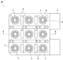
以下、本発明を実施するための形態について、図面を参照して説明する。図1は、本発明の発光装置をLEDランプに適用した実施形態の構成を示す断面図、図2は、図1に示すLEDランプの複数個を、例えば一平面上に3行3列のマトリックス状に配置したLEDモジュールの一例を示す平面図、図3は、図2のA−A´線断面図である。 Hereinafter, embodiments for carrying out the present invention will be described with reference to the drawings. FIG. 1 is a cross-sectional view showing a configuration of an embodiment in which the light-emitting device of the present invention is applied to an LED lamp. FIG. 2 is a diagram of a plurality of LED lamps shown in FIG. FIG. 3 is a cross-sectional view taken along the line AA ′ of FIG. 2.
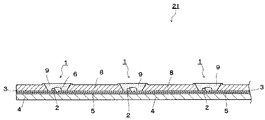
図1に示すLEDランプ1は、発光素子として、青色発光タイプのLEDチップ2を有している。このLEDチップ2は、回路パターン3を有する基板4上に搭載されている。基板4としては、放熱性と剛性を有するアルミニウム(Al)やニッケル(Ni)、ガラスエポキシ樹脂などから成る平板が用いられ、この基板4上に電気絶縁層5を介して陰極側と陽極側の回路パターン3がそれぞれ形成されている。回路パターン3は、CuとNiの合金やAuなどから構成されている。
The
そして、LEDチップ2の底面電極が一方の電極側の回路パターン3の上に配置されて電気的に接続され、上面電極が他方の電極側の回路パターン3に、金線のようなボンディングワイヤ6を介して電気的に接続されている。LEDチップ2の電極接続構造としては、フリップチップ接続構造を適用することもできる。これらの電極接続構造によれば、LEDチップ2の前面への光取出し効率が向上する。
The bottom electrode of the
基板4上には、凹部7を有する樹脂製などのフレーム8が設けられている。凹部7を有するフレーム8は、例えばPBT(ポリブチレンテレフタレート)、PPA(ポリフタルアミド)、PC(ポリカーボネート)などの合成樹脂から構成され、凹部7内にLEDチップ2が配置され、収容されている。そして、LEDチップ2が収容された凹部7内には、波長490〜510nmの範囲と波長530〜580nmの範囲にそれぞれ発光ピークを有する第1の蛍光体(緑色蛍光体)と、波長610〜660nmの範囲に発光ピークを有する第2の蛍光体(赤色蛍光体)との計2種類の蛍光体を、透明樹脂に混合し分散させた蛍光体含有樹脂が塗布・充填されており、LEDチップ2はこのような蛍光体含有樹脂層9により覆われている。透明樹脂としては、例えばシリコーン樹脂やエポキシ樹脂などが用いられる。
On the
蛍光体として、前記した第1の蛍光体である緑色蛍光体と第2の蛍光体である赤色蛍光体とともに、波長530〜580nmの範囲に発光ピークを有する黄色蛍光体(第3の蛍光体)を使用し、これら計3種類の蛍光体を混合して使用することもできる。 As a phosphor, a yellow phosphor (third phosphor) having an emission peak in the wavelength range of 530 to 580 nm, together with the green phosphor as the first phosphor and the red phosphor as the second phosphor. These three types of phosphors can be mixed and used.
緑色蛍光体は、例えばRE3(Al,Ga)5O12:Ce蛍光体(REは、Y、GdおよびLaから選ばれる少なくとも1種を示す。)などのYAG蛍光体、AE2SiO4:Eu蛍光体(AEは、Sr、Ba、Caなどのアルカリ土類元素を示す。)やCa3Sc2Si3O12:Ce蛍光体などのケイ酸塩蛍光体、サイアロン系蛍光体(例えば、CaxSiyAlzON:Eu2+)、およびCa3Sc2O4:Ce蛍光体などの中から選択される。 The green phosphor is, for example, a YAG phosphor such as RE 3 (Al, Ga) 5 O 12 : Ce phosphor (RE represents at least one selected from Y, Gd and La), AE 2 SiO 4 : Eu phosphors (AE represents alkaline earth elements such as Sr, Ba, Ca) and silicate phosphors such as Ca 3 Sc 2 Si 3 O 12 : Ce phosphors, sialon phosphors (for example, Ca x Si y Al z ON: Eu 2+ ), Ca 3 Sc 2 O 4 : Ce phosphor, and the like.
赤色蛍光体としては、La2O2S:Eu蛍光体のような酸硫化物蛍光体、窒化物系蛍光体(例えば、AE2Si5N8:Eu2+やCaAlSiN3:Eu2+)などが用いられるが、特に限定されるものではない。 Examples of the red phosphor include oxysulfide phosphors such as La 2 O 2 S: Eu phosphor, nitride phosphors (for example, AE 2 Si 5 N 8 : Eu 2+ and CaAlSiN 3 : Eu 2+ ), and the like. Although used, it is not particularly limited.
黄色蛍光体は、例えばRE3(Al,Ga)5O12:Ce蛍光体(REは、Y、GdおよびLaから選ばれる少なくとも1種を示す。)などのYAG蛍光体、(Tb,Al)5O12:Ce蛍光体などのTAG蛍光体、サイアロン系蛍光体(例えば、CaxSiyAlzON:Eu2+)、AE2SiO4:Eu蛍光体(AEは、Sr、Ba、Caなどのアルカリ土類元素を示す。)やSr3SiO5:Eu2+蛍光体などのケイ酸塩蛍光体などの中から選択される。 The yellow phosphor is, for example, a YAG phosphor such as RE 3 (Al, Ga) 5 O 12 : Ce phosphor (RE represents at least one selected from Y, Gd and La), (Tb, Al) 5 O 12 : TAG phosphor such as Ce phosphor, sialon-based phosphor (for example, Ca x Si y Al z ON: Eu 2+ ), AE 2 SiO 4 : Eu phosphor (AE is Sr, Ba, Ca, etc.) Silicate phosphors such as Sr 3 SiO 5 : Eu 2+ phosphor and the like.
そして、これら2種類または3種類の蛍光体から成る蛍光体の混合物は、以下に示す発光スペクトルを有している。すなわち、発光スペクトルの波長490〜510nmの範囲における発光ピークの強度をA、波長530〜580nmの範囲における発光ピークの強度をB、波長610〜660nmの範囲における発光ピークの強度をCとするとき、BとAの比(B/A)が0.8〜1.2であり、かつCとAの比(C/A)が0.5〜1.2となっている And the mixture of the fluorescent substance which consists of these 2 types or 3 types of fluorescent substance has the emission spectrum shown below. That is, when the emission peak intensity in the wavelength range of 490 to 510 nm of the emission spectrum is A, the emission peak intensity in the wavelength range of 530 to 580 nm is B, and the emission peak intensity in the wavelength range of 610 to 660 nm is C, The ratio of B and A (B / A) is 0.8 to 1.2, and the ratio of C and A (C / A) is 0.5 to 1.2.
BとAの比(B/A)が1.2を超えるか、あるいはCとAの比(C/A)が1.2を超えると、平均演色評価数Raが向上し高演色性は得られるが、発光効率が低くなり好ましくない。反対に、BとAの比(B/A)が0.8未満であるか、あるいはCとAの比(C/A)が0.5未満である場合には、発光の色温度の調整に対応しにくい。 When the ratio of B to A (B / A) exceeds 1.2, or the ratio of C to A (C / A) exceeds 1.2, the average color rendering index Ra is improved and high color rendering is obtained. However, the luminous efficiency is undesirably low. Conversely, when the ratio of B to A (B / A) is less than 0.8, or the ratio of C to A (C / A) is less than 0.5, the color temperature of light emission is adjusted. It is hard to cope with.
また、これら蛍光体の発光ピークの好ましい半値幅は、波長490〜510nmの発光ピークについては125〜145nm、波長530〜580nmの発光ピークについては90〜110nm、波長610〜660nmの発光ピークについては80〜100nmとすることが好ましい。半値幅が前記範囲を外れるブロードな発光ピーク、あるいはシャープすぎる発光ピークを有する蛍光体を使用した場合には、効率が高くかつ高演色性の発光を得ることが難しい。すなわち、いずれの波長範囲の発光ピークにおいても、半値幅が下限値未満のシャープすぎる発光ピークの場合には、平均演色評価数Raが低くなりすぎる。また、波長530〜580nmの発光ピークにおいて、半値幅が110nmを超えるブロードな発光ピークとした場合には、発光効率が低くなり好ましくない。波長490〜510nmの発光ピークおよび波長610〜660nmの発光ピークにおいて、半値幅が上限値を超えるブロードな発光ピークの場合には、これらの発光は視感度が比較的低いので発光効率の低下はそれほど大きくはないが、演色性向上の効果が十分に上がらない。 The preferred half-widths of the emission peaks of these phosphors are 125 to 145 nm for the emission peak at a wavelength of 490 to 510 nm, 90 to 110 nm for the emission peak of a wavelength of 530 to 580 nm, and 80 for the emission peak of a wavelength of 610 to 660 nm. It is preferable to set it to ˜100 nm. When a phosphor having a broad emission peak whose half width is out of the above range or an emission peak that is too sharp is used, it is difficult to obtain light with high efficiency and high color rendering properties. That is, in any light emission peak in any wavelength range, in the case of a light emission peak whose half width is less than the lower limit value and is too sharp, the average color rendering index Ra is too low. Moreover, in the emission peak of wavelength 530-580 nm, when it is set as the broad emission peak whose half value width exceeds 110 nm, luminous efficiency becomes low and is not preferable. In the light emission peak at a wavelength of 490 to 510 nm and the light emission peak at a wavelength of 610 to 660 nm, in the case of a broad light emission peak whose half width exceeds the upper limit, since the light emission is relatively low in visibility, the decrease in light emission efficiency is not so much. Although it is not large, the effect of improving color rendering is not sufficiently improved.
実施形態のLEDランプ1では、印加された電気エネルギーがLEDチップ2で主波長が420〜480nm(例えば460nm)の青色光に変換されて放射され、放射された青色光は、蛍光体含有樹脂層9中に含有された緑色蛍光体と赤色蛍光体の計2種類、あるいは緑色蛍光体と黄色蛍光体と赤色蛍光体の計3種類からなる蛍光体で、より長波長の光に変換される。そして、LEDチップ2から放射される青色光とこれらの蛍光体の発光色とに基づく色である白色光がLEDランプ1から放出される。
In the
そして、実施形態のLEDランプ1においては、従来のLEDランプ1の発光スペクトルには存在しなかった、主波長が490〜510nmの発光が加えられているので、十分に高い平均演色評価数Raの値を確保することができるうえに、好ましい演色性を有している。また、所望の色温度を得るために必要な主波長が610〜660nmの蛍光体(赤色蛍光体)の配合割合を、従来に比べて低減することができるので、発光効率を向上させることができる。すなわち、赤色蛍光体の配合割合を低減することにより、十分に高い演色性を維持しながら、赤色蛍光体の配合によるデメリットである発光効率の低下を抑制することができ、高演色性と高い発光効率を同時に実現することができる。
In the
また、青色発光素子から放射された青色光と、蛍光体からの発光との混色により発せられる光が、波長470〜490nmの範囲に発光強度の谷部を有しており、かつこの谷部における発光強度(D)が波長490〜510nmの範囲の発光ピークの発光強度(A)に対して、0.7〜0.95の割合となるようなスペクトルを有している。このように、視感度が低い波長範囲(470〜490nm)に発光強度の谷部が形成され、より視感度が高い波長範囲(例えば490〜510nm)への光変換がなされた発光スペクトルを有しているので、発光効率が向上している。なお、青色光の発光ピークの発光強度(E)に対する発光谷部の発光強度(D)の割合(D/E)が0.7未満では、平均演色評価数Raの大幅な低下が生じるため好ましくない。そして、谷部の波長範囲(470〜490nm)の光は視感度が低く、発光強度が高くても視覚的効果が小さいので、D/Eが0.9を超えた場合には発光効率の向上が得られず、エネルギー効率の点で好ましくない。 In addition, the light emitted by the color mixture of the blue light emitted from the blue light emitting element and the light emitted from the phosphor has a valley portion of the emission intensity in the wavelength range of 470 to 490 nm, and in this valley portion The light emission intensity (D) has a spectrum such that the ratio is 0.7 to 0.95 with respect to the light emission intensity (A) of the light emission peak in the wavelength range of 490 to 510 nm. As described above, a valley of emission intensity is formed in the wavelength range with low visibility (470 to 490 nm), and the light emission spectrum has been converted into a wavelength range with higher visibility (for example, 490 to 510 nm). Therefore, the luminous efficiency is improved. In addition, when the ratio (D / E) of the emission intensity (D) of the emission valley portion to the emission intensity (E) of the emission peak of blue light is less than 0.7, it is preferable because the average color rendering index Ra is significantly reduced. Absent. The light in the trough wavelength range (470 to 490 nm) has low visibility, and the visual effect is small even when the emission intensity is high. Therefore, when D / E exceeds 0.9, the emission efficiency is improved. Is not preferable in terms of energy efficiency.
なお、上記実施形態では、LEDランプ1をマトリックス状に複数個配置したLEDジュール21について説明したが、本発明はこれに限定されるものではなく、例えば複数個のLEDランプ1を1列状に配置して形成してもよく、さらにLEDランプ1は単数でもよい。
In the above embodiment, the
図4および図5は、本発明の第2の実施形態に係わるLEDパッケージを形成する発光装置を示している。図4は、この発光装置の平面図であり、図5は、図4に示す発光装置をF−F線に沿って切断した縦断面図である。なお、図4および図5おいて、第1の実施形態に関する図面と同様の構成要素については同じ参照数字を用いて、その説明を簡略化または省略する。 4 and 5 show a light-emitting device for forming an LED package according to the second embodiment of the present invention. 4 is a plan view of the light emitting device, and FIG. 5 is a longitudinal sectional view of the light emitting device shown in FIG. 4 cut along the line FF. 4 and 5, the same reference numerals are used for the same components as those in the drawings relating to the first embodiment, and the description thereof is simplified or omitted.
図4および図5に示す発光装置(LEDランプ)1は、パッケージ基板例えば装置基板4と、反射層31と、回路パターン3と、複数好ましくは多数の半導体発光素子(例えば青色LEDチップ)2と、接着層32と、リフレクタ34と、蛍光体含有樹脂層9と、光拡散部材33とを備えて形成されている。蛍光体含有樹脂層9は封止部材としても機能する。
A light emitting device (LED lamp) 1 shown in FIGS. 4 and 5 includes a package substrate such as a
装置基板4は、金属または絶縁材、例えば合成樹脂製の平板からなり、発光装置1に必要とされる発光面積を得るために、所定形状例えば長方形状をなしている。装置基板4を合成樹脂製とする場合、例えば、ガラス粉末入りのエポキシ樹脂等で形成することができる。装置基板4を金属製とする場合は、この装置基板4の裏面からの放熱性が向上し、装置基板4の各部温度を均一にすることができ、同じ波長域の光を発する半導体発光素子2の発光色のばらつきを抑制することができる。なお、このような作用効果を奏する金属材料としては、10W/m・K以上の熱伝導性に優れた材料、具体的にはアルミニウムまたはその合金を例示することができる。
The
反射層31は、所定数の半導体発光素子2を配設し得る大きさであって、例えば、装置基板4の表面全体に被着されている。反射層31は、400〜740nmの波長領域で85%以上の反射率を有する白色の絶縁材料により構成することができる。このような白色絶縁材料としては、接着シートからなるプリプレグ(pre-preg)を使用することができる。このようなプリプレグは、例えば、酸化アルミニウム等の白色粉末が混入された熱硬化性樹脂をシート基材に含浸させて形成することができる。反射層31はそれ自体の接着性により、装置基板4の表面となる一面に接着される。
The
回路パターン3は、各半導体発光素子2への通電要素として、反射層31の装置基板4が接着された面とは反対側の面に接着されている。この回路パターン3は、例えば各半導体発光素子2を直列に接続するために、装置基板4および反射層31の長手方向に所定間隔ごとに点在して2列に形成されている。一方の回路パターン3の列の一端側に位置する端側回路パターン3aには、給電パターン部3cが一体に連続して形成され、同様に他方の回路パターン3の列の一端側に位置する端側回路パターン3aには、給電パターン部3dが一体に連続して形成されている。
The
給電パターン部3c,3dは反射層31の長手方向一端部に並べて設けられ、互いに離間して反射層31により絶縁されている。これらの給電パターン部3c,3dのそれぞれに、電源に至る図示しない電線が個別に半田付け等で接続されるようになっている。
The power
回路パターン3は以下に説明する手順で形成される。まず、未硬化の前記熱硬化性樹脂が含浸されたプリプレグからなる反射層31を装置基板4上に貼付けた後、反射層31上にこれと同じ大きさの銅箔を貼付ける。次に、こうして得た積層体を加熱するとともに加圧して、熱硬化性樹脂を硬化させることによって、装置基板4と銅箔を反射層31に圧着し接着を完了させる。次いで、銅箔上にレジスト層を設けて、銅箔をエッチング処理した後に、残ったレジスト層を除去することによって、回路パターン3を形成する。銅箔からなる回路パターン3の厚みは例えば35μmである。
The
図5に示すように、半導体発光素子2は、例えば窒化物半導体を用いてなるダブルワイヤー型のLEDチップからなり、透光性を有する素子基板2b一面に半導体発光層2aを積層して形成されている。素子基板2bは、例えばサファイア基板で作られている。この素子基板2bの厚みは、回路パターン3より厚く、例えば90μmとする。
As shown in FIG. 5, the semiconductor
半導体発光層2aは、素子基板2bの主面上に、バッファ層、n型半導体層、発光層、p型クラッド層、p型半導体層を順次積層して形成されている。発光層は、バリア層とウェル層を交互に積層した量子井戸構造をなしている。n型半導体層にはn側電極が設けられ、p型半導体層上にはp側電極が設けられている。この半導体発光層2aは、反射膜を有しておらず、厚み方向の双方に光を放射できる。
The semiconductor
各半導体発光素子2は、装置基板4の長手方向に隣接した回路パターン3間にそれぞれ配置され、白色の反射層31の同一面上に接着層32により接着されている。具体的には、半導体発光層2aが積層された素子基板2bの一面と平行な他面が、接着層32により反射層31に接着されている。この接着により、回路パターン3および半導体発光素子2は反射層31の同一面上で直線状に並べられるので、この並び方向に位置した半導体発光素子2の側面と回路パターン3とは、近接して対向するように設けられている。
Each semiconductor
接着層32の厚みは、例えば5μm以下とすることができる。接着層32には、例えば5μm以下の厚みで光透過率が70%以上の透光性を有した接着剤、例えばシリコーン樹脂系の接着剤を好適に使用できる。
The thickness of the
図4および図5に示すように、各半導体発光素子2の電極と半導体発光素子2の両側に近接配置された回路パターン3とは、ボンディングワイヤ6で接続されている。さらに、前記2列の回路パターン3列の他端側に位置された端側回路パターン3b同士も、ボンディングワイヤ6で接続されている。したがって、この実施形態の場合、各半導体発光素子2は直列に接続されている。
As shown in FIGS. 4 and 5, the electrode of each semiconductor
以上の装置基板4、反射層31、回路パターン3、各半導体発光素子2、接着層32、およびボンディングワイヤ6により、発光装置1の面発光源が形成されている。
The surface light source of the
リフレクタ34は、一個一個または数個の半導体発光素子2ごとに個別に設けられるものではなく、反射層31上の全ての半導体発光素子2を包囲する単一のものであり、例えば長方形の枠で形成されており、半導体発光素子2は前記枠で形成された凹部7内に配置されている。リフレクタ34は反射層31に接着止めされていて、その内部に複数の半導体発光素子2および回路パターン3が収められているとともに、前記一対の給電パターン部3c、3dはリフレクタ34の外部に位置されている。
The
リフレクタ34は、例えば合成樹脂で成形することができ、その内周面は反射面となっている。リフレクタ34の反射面は、AlやNi等の反射率の高い金属材料を蒸着またはメッキして形成することができる他、可視光の反射率の高い白色塗料を塗布して形成することができる。あるいは、リフレクタ34の成形材料中に白色粉末を混入して、リフレクタ34自体を可視光の反射率が高い白色にすることもできる。前記白色粉末としては、酸化アルミニウム、酸化チタン、酸化マグネシウム、硫酸バリウム等の白色フイラーを用いることができる。なお、リフレクタ34の反射面は、発光装置1の照射方向に次第に開くように形成することが望ましい。
The
蛍光体含有樹脂層9は、前記第1の実施形態と同様に、2種類あるいは3種類の蛍光体を混合した液状の熱硬化性樹脂をディスペンサ等の注入装置を用いて、反射層31表面および一直線上に配列された各半導体発光素子2およびボンディングワイヤ6等を満遍なく埋めるようにして充填し、加熱により熱硬化性樹脂を硬化させることにより形成されている。
As in the first embodiment, the phosphor-containing resin layer 9 is formed by using a liquid thermosetting resin in which two or three kinds of phosphors are mixed using an injection device such as a dispenser and the surface of the
反射層31表面とボンディングワイヤ6との間に流れ込んだ液状の透明樹脂は、毛細管現象等により各半導体発光素子2およびボンディングワイヤ6に行きわたり、その膜厚等がほぼ均一になっており、蛍光体も透明樹脂にほぼ均一に分散している。
The liquid transparent resin that flows between the surface of the
このように構成される第2の実施形態においても、十分に高い平均演色評価数Raの値を確保することができるうえに、好ましい演色性を有している。また、エネルギー効率の向上を図ることができ、高い発光効率を得ることができる。 Also in the second embodiment configured as described above, a sufficiently high value of the average color rendering index Ra can be ensured, and preferable color rendering properties are provided. In addition, energy efficiency can be improved and high luminous efficiency can be obtained.
次に、本発明の実施例およびその評価結果について記載する。 Next, examples of the present invention and evaluation results thereof will be described.
実施例1,2、比較例
波長500nmと波長550nmにそれぞれ発光ピークを有する緑色蛍光体(YAG蛍光体)と、波長650nmに発光ピークを有する赤色蛍光体とを、それぞれシリコーン樹脂中に表1に示す配合比(シリコーン樹脂に対する配合割合;重量%)で混合し、分散させた。実施例2では、主波長が650nmの赤色蛍光体の配合比を、実施例1に比べて減少させた。また、比較例においては、波長540nmに発光ピークを有する黄色蛍光体(YAG蛍光体)を使用し、この蛍光体と主波長が650nmの赤色蛍光体とを、表1に示す配合比でシリコーン樹脂中に混合して、分散させた。
Examples 1 and 2 and Comparative Examples Table 1 shows green phosphors (YAG phosphors) each having an emission peak at a wavelength of 500 nm and a wavelength of 550 nm, and red phosphors having an emission peak at a wavelength of 650 nm. The mixture was mixed and dispersed at the indicated blending ratio (blending ratio with respect to the silicone resin; wt%). In Example 2, the compounding ratio of the red phosphor having a dominant wavelength of 650 nm was decreased as compared with Example 1. Further, in the comparative example, a yellow phosphor having a light emission peak at a wavelength of 540 nm (YAG phosphor) is used, and this phosphor and a red phosphor having a dominant wavelength of 650 nm are mixed with a silicone resin at a blending ratio shown in Table 1. Mixed in and dispersed.
次に、こうして得られた蛍光体含有シリコーン樹脂を、開口径3mmの凹部8内に充填した後、シリコーン樹脂を硬化させて蛍光体含有樹脂層9を形成し、図1に示す構成を有するLEDランプ1を作製した。なお、蛍光体含有樹脂層9の光路長は0.45mmとした。光路長は、LEDチップの上面より光取り出し側の蛍光体含有樹脂層の厚さをいう
Next, after filling the phosphor-containing silicone resin thus obtained into the
こうして実施例1,2および比較例で得られたLEDランプを発光させ、発光の色温度と平均演色評価数Raおよび発光効率をそれぞれ測定した。これらの測定結果を表1に示す。なお、発光効率は、比較例のLEDランプの発光効率100%としたときの相対値である。 Thus, the LED lamps obtained in Examples 1 and 2 and the comparative example were caused to emit light, and the color temperature of light emission, the average color rendering index Ra, and the light emission efficiency were measured, respectively. These measurement results are shown in Table 1. The luminous efficiency is a relative value when the luminous efficiency of the LED lamp of the comparative example is 100%.
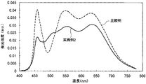
また、これらのLEDランプの発光スペクトルを分光光度計(大塚電子製の瞬間分光度計MCPD−7000)を用いて測定した。そして、波長500nmの発光ピークの強度A、波長550nmの発光ピークの強度B、波長650nmの発光ピークの強度Cをそれぞれ測定し、BとAの比(B/A)およびCとAの比(C/A)をそれぞれ求めた。これらの結果を表1に示す。さらに、実施例2および比較例で得られたLEDランプの発光スペクトルを、図6に示す。 The emission spectra of these LED lamps were measured using a spectrophotometer (instant spectrophotometer MCPD-7000 manufactured by Otsuka Electronics). Then, the intensity A of the emission peak at the wavelength of 500 nm, the intensity B of the emission peak at the wavelength of 550 nm, and the intensity C of the emission peak at the wavelength of 650 nm are measured, respectively, and the ratio of B to A (B / A) and the ratio of C to A ( C / A) was determined. These results are shown in Table 1. Furthermore, the emission spectrum of the LED lamp obtained in Example 2 and the comparative example is shown in FIG.

表1から明らかなように、実施例1および実施例2で得られたLEDランプは、波長550nmの発光ピークと波長650nmの発光ピークとともに、波長500nm付近にも発光ピークを有する蛍光体を含有しているので、高演色性の発光が得られ、平均演色評価数Raを向上させることができる。 As is apparent from Table 1, the LED lamps obtained in Example 1 and Example 2 contain a phosphor having an emission peak at a wavelength of 550 nm and an emission peak at a wavelength of 650 nm, and also having an emission peak in the vicinity of a wavelength of 500 nm. Therefore, light emission with high color rendering properties can be obtained, and the average color rendering index Ra can be improved.
特に、実施例2で得られたLEDランプは、図6の発光スペクトルからわかるように、視感度の低い波長470〜490nmの範囲(480nm)に発光強度の谷部を有し、この谷部(波長480nm)における発光強度(D)の青色光の発光ピーク(波長460nm)の発光強度(E)に対する割合が、0.85となっている。そして、実施例2のLEDランプは、実施例1および比較例のLEDランプと同様の色温度を有するにも関わらず、平均演色評価数Raが92と、比較例のLEDランプより高い演色性を有する。また、発光効率が実施例1のものよりも30%向上しており、極めて高い発光効率を有している。それに対して、比較例のLEDランプの発光スペクトルは、波長470〜490nmの範囲(480nm)に発光強度の谷部を有しておらず、平均演色評価数Raと発光効率がともに実施例2より低くなっている。 In particular, as can be seen from the emission spectrum of FIG. 6, the LED lamp obtained in Example 2 has a valley of emission intensity in a wavelength range of 470 to 490 nm (480 nm) with low visibility, and this valley ( The ratio of the emission intensity (D) at the wavelength 480 nm) to the emission intensity (E) of the emission peak of blue light (wavelength 460 nm) is 0.85. And although the LED lamp of Example 2 has the color temperature similar to the LED lamp of Example 1 and a comparative example, average color rendering index Ra is 92 and has higher color rendering than the LED lamp of a comparative example. Have. In addition, the luminous efficiency is 30% higher than that of Example 1, and the luminous efficiency is extremely high. On the other hand, the emission spectrum of the LED lamp of the comparative example does not have a valley of emission intensity in the wavelength range of 470 to 490 nm (480 nm), and both the average color rendering index Ra and the emission efficiency are from Example 2. It is low.
実施例3〜12
実施例3〜6においては、波長500nmと波長550nmにそれぞれ発光ピークを有する緑色蛍光体(YAG蛍光体)と波長650nmに発光ピークを有する赤色蛍光体との2種類の蛍光体を使用した。また、実施例7〜12においては、前記緑色蛍光体(YAG蛍光体)および赤色蛍光体に、波長565nmに発光ピークを有する黄色蛍光体(YAG蛍光体)を加え、計3種類の蛍光体を使用した。そして、これらの蛍光体をそれぞれシリコーン樹脂中に、表2に示す配合比(シリコーン樹脂に対する配合割合;重量%)で混合し、分散させた。
Examples 3-12
In Examples 3 to 6, two types of phosphors were used: a green phosphor having an emission peak at a wavelength of 500 nm and a wavelength of 550 nm (YAG phosphor) and a red phosphor having an emission peak at a wavelength of 650 nm. In Examples 7 to 12, a yellow phosphor having an emission peak at a wavelength of 565 nm (YAG phosphor) is added to the green phosphor (YAG phosphor) and the red phosphor, and a total of three types of phosphors are obtained. used. Each of these phosphors was mixed and dispersed in the silicone resin at a blending ratio shown in Table 2 (blending ratio with respect to the silicone resin: wt%).
次に、こうして得られた蛍光体含有シリコーン樹脂を、実施例1,2と同様に、開口径3mmの凹部8内に充填した後、シリコーン樹脂を硬化させて蛍光体含有樹脂層9を形成し、図1に示す構成を有するLEDランプ1を作製した。なお、実施例3〜12においては、実施例1,2に比べて樹脂に対する蛍光体の配合比を小さくしたので、同程度の色を実現するために、蛍光体含有樹脂層9の光路長を0.9mmと長くした。発光色および発光強度を同等にするには、光路長と蛍光体の配合比との積を等しくする必要がある。
Next, after the phosphor-containing silicone resin thus obtained was filled into the
こうして実施例3〜12で得られたLEDランプを発光させ、発光の色温度と平均演色評価数Raおよび発光効率をそれぞれ測定した。これらの測定結果を表2に示す。なお、発光効率は、実施例7のLEDランプの発光効率100%としたときの相対値である。 Thus, the LED lamps obtained in Examples 3 to 12 were caused to emit light, and the color temperature of light emission, the average color rendering index Ra, and the light emission efficiency were measured. These measurement results are shown in Table 2. The luminous efficiency is a relative value when the luminous efficiency of the LED lamp of Example 7 is 100%.
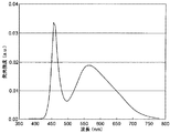
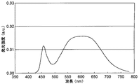
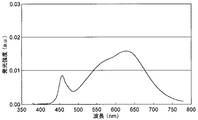
また、発光スペクトルを分光光度計(大塚電子製の瞬間分光度計MCPD−7000)を用いて測定した。これらのスペクトルのうち、実施例4で得られたLEDランプの発光スペクトルを図7に、実施例6で得られたLEDランプの発光スペクトルを図8に、実施例8で得られたLEDランプの発光スペクトルを図9に、実施例9で得られたLEDランプの発光スペクトルを図10に、実施例11で得られたLEDランプの発光スペクトルを図11に、実施例12で得られたLEDランプの発光スペクトルを図12にそれぞれ示す。 The emission spectrum was measured using a spectrophotometer (instant spectrophotometer MCPD-7000 manufactured by Otsuka Electronics Co., Ltd.). Of these spectra, the emission spectrum of the LED lamp obtained in Example 4 is shown in FIG. 7, the emission spectrum of the LED lamp obtained in Example 6 is shown in FIG. 8, and the emission spectrum of the LED lamp obtained in Example 8 is shown. FIG. 9 shows the emission spectrum, FIG. 10 shows the emission spectrum of the LED lamp obtained in Example 9, FIG. 11 shows the emission spectrum of the LED lamp obtained in Example 11, and FIG. 11 shows the LED lamp obtained in Example 12. The emission spectra are shown in FIG.
さらに、これらのLEDランプの発光スペクトルから、波長470〜490nmの範囲(例えば480nm)の谷部の発光強度(D)の波長460nmの発光強度(E)に対する割合(谷部強度比D/E)を求めた。これらの結果も表2に示す。 Furthermore, from the emission spectrum of these LED lamps, the ratio of the emission intensity (D) at the valley in the wavelength range of 470 to 490 nm (for example, 480 nm) to the emission intensity (E) at the wavelength of 460 nm (valley intensity ratio D / E). Asked. These results are also shown in Table 2.
表2の測定結果、ならびに図7〜12の発光スペクトルから、以下のことがわかる。すなわち、実施例3〜12で得られたLEDランプは、波長550nm付近と波長650nm付近にそれぞれ発光ピークを有するとともに、波長500nm付近にも発光ピークを有しており、平均演色評価数Raが高く、かつ十分に高い発光効率を有している。 From the measurement results of Table 2 and the emission spectra of FIGS. That is, the LED lamps obtained in Examples 3 to 12 have emission peaks near the wavelength of 550 nm and near the wavelength of 650 nm, respectively, and also have emission peaks near the wavelength of 500 nm, and the average color rendering index Ra is high. And has a sufficiently high luminous efficiency.
また、実施例4,6,8.9,11,12および実施例2で得られたLEDランプの発光スペクトルからわかるように、谷部強度比(D/E)が0.7〜0.9の場合に、特に色温度3000〜4000Kにおいて、平均演色評価数Raが90以上と高く、LEDランプとして好適である。また、緑色蛍光体と赤色蛍光体の2種類の蛍光体を使用した実施例3〜6のLEDランプでは、発光効率はそれほど高いものではないが、平均演色評価数Raが90〜95と極めて高い演色性を有する発光が得られる。これに対して、緑色蛍光体と赤色蛍光体および黄色蛍光体の計3種類の蛍光体を使用した実施例7〜12のLEDランプでは、平均演色評価数Raは80程度であっても、極めて高い発光効率を有する発光が得られる。 Further, as can be seen from the emission spectra of the LED lamps obtained in Examples 4, 6, 8.9, 11, 12 and Example 2, the valley intensity ratio (D / E) is 0.7 to 0.9. In this case, particularly at a color temperature of 3000 to 4000 K, the average color rendering index Ra is as high as 90 or more, which is suitable as an LED lamp. In addition, in the LED lamps of Examples 3 to 6 using two types of phosphors, a green phosphor and a red phosphor, the luminous efficiency is not so high, but the average color rendering index Ra is as high as 90 to 95. Luminescence having color rendering properties can be obtained. On the other hand, in the LED lamps of Examples 7 to 12 using a total of three types of phosphors, that is, a green phosphor, a red phosphor, and a yellow phosphor, even if the average color rendering index Ra is about 80, Luminescence having high luminous efficiency can be obtained.
1…LEDランプ、2…LEDチップ、3…回路パターン、4…基板、6…ボンディングワイヤ、7…凹部、8…フレーム、9…蛍光体含有樹脂層。
DESCRIPTION OF
Claims (9)
前記発光素子から放射された青色光により励起されて、波長490〜510nmと530〜580nmおよび610〜660nmにそれぞれピークを有する光を発光する蛍光体を含有する蛍光体層と;
を具備することを特徴とする発光装置。 A light emitting device emitting blue light;
A phosphor layer containing a phosphor that is excited by blue light emitted from the light emitting element and emits light having peaks at wavelengths of 490 to 510 nm, 530 to 580 nm, and 610 to 660 nm;
A light-emitting device comprising:
前記青色発光素子から放射された青色光により励起されて、波長490〜510nmと530〜580nmおよび610〜660nmにそれぞれ発光ピークを有するとともに、前記青色光との混色により、波長470〜490nmに発光強度の谷部を有し、かつ前記青色光の発光ピークの発光強度に対する前記谷部の発光強度の割合が0.7〜0.9である可視光を発する蛍光体を含有する蛍光体層と;
を具備することを特徴とする発光装置。 A blue light emitting element emitting blue light;
Excited by blue light emitted from the blue light emitting element, has emission peaks at wavelengths of 490 to 510 nm, 530 to 580 nm, and 610 to 660 nm, respectively, and the emission intensity at wavelengths of 470 to 490 nm due to color mixture with the blue light. And a phosphor layer containing a phosphor that emits visible light, the ratio of the emission intensity of the valley to the emission intensity of the emission peak of the blue light being 0.7 to 0.9;
A light-emitting device comprising:
Priority Applications (1)
| Application Number | Priority Date | Filing Date | Title |
|---|---|---|---|
| JP2007019580A JP2007266579A (en) | 2006-02-28 | 2007-01-30 | Light emitting device |
Applications Claiming Priority (2)
| Application Number | Priority Date | Filing Date | Title |
|---|---|---|---|
| JP2006053708 | 2006-02-28 | ||
| JP2007019580A JP2007266579A (en) | 2006-02-28 | 2007-01-30 | Light emitting device |
Publications (2)
| Publication Number | Publication Date |
|---|---|
| JP2007266579A true JP2007266579A (en) | 2007-10-11 |
| JP2007266579A5 JP2007266579A5 (en) | 2009-11-05 |
Family
ID=38639217
Family Applications (1)
| Application Number | Title | Priority Date | Filing Date |
|---|---|---|---|
| JP2007019580A Pending JP2007266579A (en) | 2006-02-28 | 2007-01-30 | Light emitting device |
Country Status (1)
| Country | Link |
|---|---|
| JP (1) | JP2007266579A (en) |
Cited By (17)
| Publication number | Priority date | Publication date | Assignee | Title |
|---|---|---|---|---|
| WO2011112342A2 (en) * | 2010-03-09 | 2011-09-15 | Cree, Inc. | High cri lighting device with added long-wavelength blue color |
| JP2012507115A (en) * | 2008-10-24 | 2012-03-22 | クリー インコーポレイテッド | Lighting device, heat transfer structure, and heat transfer element |
| WO2012104937A1 (en) | 2011-02-03 | 2012-08-09 | パナソニック株式会社 | Led module and illumination device |
| JP2013058473A (en) * | 2011-08-18 | 2013-03-28 | Panasonic Corp | Illumination device |
| US8410680B2 (en) | 2005-01-10 | 2013-04-02 | Cree, Inc. | Multi-chip light emitting device lamps for providing high-CRI warm white light and light fixtures including the same |
| US8513873B2 (en) | 2005-01-10 | 2013-08-20 | Cree, Inc. | Light emission device |
| CN103594607A (en) * | 2012-08-13 | 2014-02-19 | 松下电器产业株式会社 | Lighting device |
| US8884508B2 (en) | 2011-11-09 | 2014-11-11 | Cree, Inc. | Solid state lighting device including multiple wavelength conversion materials |
| JPWO2013069435A1 (en) * | 2011-11-07 | 2015-04-02 | 株式会社東芝 | White light source and white light source system using the same |
| US9030103B2 (en) | 2013-02-08 | 2015-05-12 | Cree, Inc. | Solid state light emitting devices including adjustable scotopic / photopic ratio |
| US9039746B2 (en) | 2013-02-08 | 2015-05-26 | Cree, Inc. | Solid state light emitting devices including adjustable melatonin suppression effects |
| US9190582B2 (en) | 2013-04-03 | 2015-11-17 | Kabushiki Kaisha Toshiba | Light emitting device |
| US9240528B2 (en) | 2013-10-03 | 2016-01-19 | Cree, Inc. | Solid state lighting apparatus with high scotopic/photopic (S/P) ratio |
| JP2016139516A (en) * | 2015-01-27 | 2016-08-04 | パイオニア株式会社 | Luminaire |
| JP2016146283A (en) * | 2015-02-09 | 2016-08-12 | パナソニックIpマネジメント株式会社 | Light emitting device, lighting fixture and lighting system |
| CN106287552A (en) * | 2015-06-26 | 2017-01-04 | 松下知识产权经营株式会社 | Illumination light source and illuminator |
| KR101855391B1 (en) | 2016-12-26 | 2018-05-09 | 지엘비텍 주식회사 | White Light Emitting Device with High Color Rendering Index |
Citations (5)
| Publication number | Priority date | Publication date | Assignee | Title |
|---|---|---|---|---|
| JP2002363554A (en) * | 2001-06-07 | 2002-12-18 | National Institute For Materials Science | Acid nitride phosphor activated with rare earth element |
| JP2003513474A (en) * | 1999-11-03 | 2003-04-08 | オスラム オプト セミコンダクターズ ゲゼルシャフト ミット ベシュレンクテル ハフツング | Light-emitting diode white light source with broadband excitation |
| JP2004210921A (en) * | 2002-12-27 | 2004-07-29 | Nichia Chem Ind Ltd | Oxynitride fluorophor and method for producing the same and light-emitting device using the same |
| JP2005112922A (en) * | 2003-10-03 | 2005-04-28 | National Institute For Materials Science | Oxynitride phosphor |
| JP2005340748A (en) * | 2003-09-18 | 2005-12-08 | Nichia Chem Ind Ltd | Light emitting device |
-
2007
- 2007-01-30 JP JP2007019580A patent/JP2007266579A/en active Pending
Patent Citations (5)
| Publication number | Priority date | Publication date | Assignee | Title |
|---|---|---|---|---|
| JP2003513474A (en) * | 1999-11-03 | 2003-04-08 | オスラム オプト セミコンダクターズ ゲゼルシャフト ミット ベシュレンクテル ハフツング | Light-emitting diode white light source with broadband excitation |
| JP2002363554A (en) * | 2001-06-07 | 2002-12-18 | National Institute For Materials Science | Acid nitride phosphor activated with rare earth element |
| JP2004210921A (en) * | 2002-12-27 | 2004-07-29 | Nichia Chem Ind Ltd | Oxynitride fluorophor and method for producing the same and light-emitting device using the same |
| JP2005340748A (en) * | 2003-09-18 | 2005-12-08 | Nichia Chem Ind Ltd | Light emitting device |
| JP2005112922A (en) * | 2003-10-03 | 2005-04-28 | National Institute For Materials Science | Oxynitride phosphor |
Cited By (26)
| Publication number | Priority date | Publication date | Assignee | Title |
|---|---|---|---|---|
| US8513873B2 (en) | 2005-01-10 | 2013-08-20 | Cree, Inc. | Light emission device |
| US8847478B2 (en) | 2005-01-10 | 2014-09-30 | Cree, Inc. | Multi-chip light emitting device lamps for providing high-CRI warm white light and light fixtures including the same |
| US8410680B2 (en) | 2005-01-10 | 2013-04-02 | Cree, Inc. | Multi-chip light emitting device lamps for providing high-CRI warm white light and light fixtures including the same |
| US8858032B2 (en) | 2008-10-24 | 2014-10-14 | Cree, Inc. | Lighting device, heat transfer structure and heat transfer element |
| JP2012507115A (en) * | 2008-10-24 | 2012-03-22 | クリー インコーポレイテッド | Lighting device, heat transfer structure, and heat transfer element |
| US10495295B2 (en) | 2008-10-24 | 2019-12-03 | Ideal Industries Lighting Llc | Lighting device, heat transfer structure and heat transfer element |
| US8508127B2 (en) | 2010-03-09 | 2013-08-13 | Cree, Inc. | High CRI lighting device with added long-wavelength blue color |
| US8508117B2 (en) | 2010-03-09 | 2013-08-13 | Cree, Inc. | High CRI lighting device with added long-wavelength blue color |
| WO2011112342A3 (en) * | 2010-03-09 | 2011-12-22 | Cree, Inc. | High cri lighting device with added long-wavelength blue color |
| WO2011112342A2 (en) * | 2010-03-09 | 2011-09-15 | Cree, Inc. | High cri lighting device with added long-wavelength blue color |
| WO2012104937A1 (en) | 2011-02-03 | 2012-08-09 | パナソニック株式会社 | Led module and illumination device |
| US8933620B2 (en) | 2011-02-03 | 2015-01-13 | Panasonic Intellectual Property Management Co., Ltd. | White light LED module with green and red phosphors and illumination device having the same |
| JP2013058473A (en) * | 2011-08-18 | 2013-03-28 | Panasonic Corp | Illumination device |
| JPWO2013069435A1 (en) * | 2011-11-07 | 2015-04-02 | 株式会社東芝 | White light source and white light source system using the same |
| US8884508B2 (en) | 2011-11-09 | 2014-11-11 | Cree, Inc. | Solid state lighting device including multiple wavelength conversion materials |
| CN103594607A (en) * | 2012-08-13 | 2014-02-19 | 松下电器产业株式会社 | Lighting device |
| US9030103B2 (en) | 2013-02-08 | 2015-05-12 | Cree, Inc. | Solid state light emitting devices including adjustable scotopic / photopic ratio |
| US9039746B2 (en) | 2013-02-08 | 2015-05-26 | Cree, Inc. | Solid state light emitting devices including adjustable melatonin suppression effects |
| US9661715B2 (en) | 2013-02-08 | 2017-05-23 | Cree, Inc. | Solid state light emitting devices including adjustable melatonin suppression effects |
| US9190582B2 (en) | 2013-04-03 | 2015-11-17 | Kabushiki Kaisha Toshiba | Light emitting device |
| US9240528B2 (en) | 2013-10-03 | 2016-01-19 | Cree, Inc. | Solid state lighting apparatus with high scotopic/photopic (S/P) ratio |
| JP2016139516A (en) * | 2015-01-27 | 2016-08-04 | パイオニア株式会社 | Luminaire |
| JP2016146283A (en) * | 2015-02-09 | 2016-08-12 | パナソニックIpマネジメント株式会社 | Light emitting device, lighting fixture and lighting system |
| CN106287552A (en) * | 2015-06-26 | 2017-01-04 | 松下知识产权经营株式会社 | Illumination light source and illuminator |
| CN106287552B (en) * | 2015-06-26 | 2019-05-17 | 松下知识产权经营株式会社 | Illumination light source and lighting device |
| KR101855391B1 (en) | 2016-12-26 | 2018-05-09 | 지엘비텍 주식회사 | White Light Emitting Device with High Color Rendering Index |
Similar Documents
| Publication | Publication Date | Title |
|---|---|---|
| JP2007266579A (en) | Light emitting device | |
| JP5181505B2 (en) | Light emitting device | |
| JP5233170B2 (en) | LIGHT EMITTING DEVICE, RESIN MOLDED BODY FORMING LIGHT EMITTING DEVICE, AND METHOD FOR PRODUCING THEM | |
| JP2009065137A (en) | Light-emitting device | |
| JP2008270781A (en) | Light-emitting device | |
| JP2008218486A (en) | Light emitting device | |
| JP5598323B2 (en) | Light emitting device and method for manufacturing light emitting device | |
| JP5194675B2 (en) | Light emitting device | |
| JP2007273562A (en) | Semiconductor light-emitting device | |
| JP2006253336A (en) | Light source device | |
| JP5082427B2 (en) | Light emitting device | |
| JP2007116133A (en) | Light emitting device | |
| JP2007116117A (en) | Light emitting device | |
| JP2009111273A (en) | Light-emitting device | |
| JP2008218998A (en) | Light emitting device | |
| JP2007288138A (en) | Light emitting device | |
| JP2007258620A (en) | Light emitting device | |
| JP2008140934A (en) | Light emitting diode device and lighting device | |
| JP2008244468A (en) | Light-emitting device | |
| JP2008235552A (en) | Method of manufacturing light-emitting apparatus and light-emitting apparatus | |
| JP2007235104A (en) | Light emitting device and manufacturing method thereof | |
| JP2009010308A (en) | Light emitting device | |
| JP2007116116A (en) | Light emitting device | |
| JP2008244469A (en) | Light-emitting device | |
| JP4986282B2 (en) | Light emitting device |
Legal Events
| Date | Code | Title | Description |
|---|---|---|---|
| A521 | Written amendment |
Free format text: JAPANESE INTERMEDIATE CODE: A523 Effective date: 20090911 |
|
| A621 | Written request for application examination |
Free format text: JAPANESE INTERMEDIATE CODE: A621 Effective date: 20090911 |
|
| A131 | Notification of reasons for refusal |
Free format text: JAPANESE INTERMEDIATE CODE: A131 Effective date: 20111220 |
|
| A977 | Report on retrieval |
Free format text: JAPANESE INTERMEDIATE CODE: A971007 Effective date: 20111221 |
|
| A02 | Decision of refusal |
Free format text: JAPANESE INTERMEDIATE CODE: A02 Effective date: 20120410 |