JP2007258263A - Organic solar cell - Google Patents
Organic solar cell Download PDFInfo
- Publication number
- JP2007258263A JP2007258263A JP2006077509A JP2006077509A JP2007258263A JP 2007258263 A JP2007258263 A JP 2007258263A JP 2006077509 A JP2006077509 A JP 2006077509A JP 2006077509 A JP2006077509 A JP 2006077509A JP 2007258263 A JP2007258263 A JP 2007258263A
- Authority
- JP
- Japan
- Prior art keywords
- electron donor
- organic
- layer
- solar cell
- organic electron
- Prior art date
- Legal status (The legal status is an assumption and is not a legal conclusion. Google has not performed a legal analysis and makes no representation as to the accuracy of the status listed.)
- Pending
Links
Images

Classifications
-
- Y—GENERAL TAGGING OF NEW TECHNOLOGICAL DEVELOPMENTS; GENERAL TAGGING OF CROSS-SECTIONAL TECHNOLOGIES SPANNING OVER SEVERAL SECTIONS OF THE IPC; TECHNICAL SUBJECTS COVERED BY FORMER USPC CROSS-REFERENCE ART COLLECTIONS [XRACs] AND DIGESTS
- Y02—TECHNOLOGIES OR APPLICATIONS FOR MITIGATION OR ADAPTATION AGAINST CLIMATE CHANGE
- Y02E—REDUCTION OF GREENHOUSE GAS [GHG] EMISSIONS, RELATED TO ENERGY GENERATION, TRANSMISSION OR DISTRIBUTION
- Y02E10/00—Energy generation through renewable energy sources
- Y02E10/50—Photovoltaic [PV] energy
- Y02E10/549—Organic PV cells
Landscapes
- Photovoltaic Devices (AREA)
Abstract
Description
本発明は、有機太陽電池に関する。 The present invention relates to an organic solar cell.
有機半導体を用いた太陽電池(有機太陽電池)は、多様性があること、毒性が低いこと、加工性・生産性が良好で大量生産によるコストダウンが可能であること、フレキシブル化が容易であり使用範囲が広いこと、などの優れた特長を有しており、現在開発が盛んに行われている。 Solar cells using organic semiconductors (organic solar cells) are diverse, have low toxicity, have good processability and productivity, can be reduced in cost by mass production, and are easily flexible It has excellent features such as a wide range of use and is currently under active development.
ここで、一般的に有機太陽電池は、無機半導体を用いた太陽電池に比べて光電変換効率が劣るため、光電交換効率を向上すべく種々の開発がなされている(例えば、特許文献1)。 Here, since an organic solar cell is generally inferior in photoelectric conversion efficiency as compared with a solar cell using an inorganic semiconductor, various developments have been made to improve the photoelectric exchange efficiency (for example, Patent Document 1).
上述の如く、有機太陽電池の光電交換効率を向上すべく種々の開発がなされているが、未だ実用化レベルに達するものは少ないのが現状である。本願発明者にあっても、有機太陽電池の光電交換効率を向上すべく研究を重ねた結果、有機太陽電池を構成する有機電子供与体層の厚さに着目するに至った。 As described above, various developments have been made to improve the photoelectric exchange efficiency of organic solar cells, but there are few that have reached a practical level yet. Even in the present inventor, as a result of repeated studies to improve the photoelectric exchange efficiency of the organic solar cell, attention has been paid to the thickness of the organic electron donor layer constituting the organic solar cell.
つまり、有機電子供与体層と電子受容体層とから形成されるヘテロ接合を有する光電変換層を備える有機太陽電池において、光電変換効率を向上させるためには、有機電子供与体層への光の吸収を最大化することが考えられ、これを実現するためには、当該有機電子供与体層の厚さをできるだけ厚くすることが必要となる。しかしながら、有機電子供与体層は抵抗が大きいため、光の吸収のみを考慮して層を厚く設計すると、電流が流れ難くなり素子特性が不良となる。逆に有機電子供与体層の電流の流れのみを考慮した場合、有機電子供与体層の厚さをできるだけ薄く設計することとなり、これでは光の吸収を充分に行うことができない。従って、有機電子供与体層への光の吸収と、当該層の電流の流れのみをもって有機電子供与体層の厚さを設計し有機太陽電池の光電交換効率を向上せしめることは難しい。 That is, in an organic solar cell including a photoelectric conversion layer having a heterojunction formed from an organic electron donor layer and an electron acceptor layer, in order to improve the photoelectric conversion efficiency, light to the organic electron donor layer is It is conceivable to maximize absorption, and in order to realize this, it is necessary to make the organic electron donor layer as thick as possible. However, since the organic electron donor layer has a large resistance, if the layer is designed to be thick considering only light absorption, current does not flow easily, resulting in poor device characteristics. Conversely, when only the current flow of the organic electron donor layer is taken into consideration, the thickness of the organic electron donor layer is designed to be as thin as possible, and this cannot sufficiently absorb light. Therefore, it is difficult to improve the photoelectric exchange efficiency of the organic solar cell by designing the thickness of the organic electron donor layer only by absorbing light into the organic electron donor layer and the current flow of the layer.
また、有機太陽電池の性能を表すパラメータとしては、前述の光電交換効率の他、短絡電流値(Jsc)、開放電圧値(Voc)、およびフィルファクター値などがあり、それぞれの値は、いずれも前記電子供与体層の厚さに依存していることが知られている。 In addition to the photoelectric exchange efficiency described above, parameters representing the performance of the organic solar cell include a short-circuit current value (Jsc), an open-circuit voltage value (Voc), a fill factor value, and the like. It is known that it depends on the thickness of the electron donor layer.
従って、これらの各パラメータの値から有機電子供与体層の最適な厚さを設計することも考えられるが、これらのパラメータの値は、別個独立して前記電子供与体層の厚さに依存しているためトレードオフの関係にあり、これらのパラメータの値のみから最適な有機電子供与体層の厚さを設計し、有機太陽電池の光電交換効率を向上せしめることも困難である。 Therefore, it is conceivable to design the optimum thickness of the organic electron donor layer from the values of these parameters, but the values of these parameters depend independently on the thickness of the electron donor layer. Therefore, there is a trade-off relationship, and it is difficult to improve the photoelectric exchange efficiency of the organic solar cell by designing the optimum thickness of the organic electron donor layer only from the values of these parameters.
本願は、このような状況下においてなされたものであり、有機太陽電池の光電交換効率を向上することを主たる課題とし、より具体的には、有機太陽電池を構成する有機電子供与体層の厚さが適当に設計されていることにより光電交換効率が良好な有機太陽電池を提供することを主たる課題とする。 The present application has been made under such circumstances, and the main object is to improve the photoelectric exchange efficiency of the organic solar cell, and more specifically, the thickness of the organic electron donor layer constituting the organic solar cell. The main object is to provide an organic solar cell with good photoelectric exchange efficiency by being appropriately designed.
上記課題を解決するための請求項1の発明は、少なくとも、有機電子供与体層と電子受容体層とから形成されるヘテロ接合を有する光電変換層と、この光電変換層を挟持する一対の電極とを備える有機太陽電池であって、前記有機電子供与体層の厚さが、これを構成する有機電子供与体の励起子拡散長の2〜5倍であることを特徴とする。 The invention according to claim 1 for solving the above-described problem includes at least a photoelectric conversion layer having a heterojunction formed of an organic electron donor layer and an electron acceptor layer, and a pair of electrodes sandwiching the photoelectric conversion layer The thickness of the organic electron donor layer is 2 to 5 times the exciton diffusion length of the organic electron donor constituting the organic solar cell.
以下に、本願の有機太陽電池について、図面を用いて具体的に説明する。 Below, the organic solar cell of this application is concretely demonstrated using drawing.
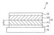
図1は、本願の有機太陽電池の構成を説明するための概略断面図である。 FIG. 1 is a schematic cross-sectional view for explaining the configuration of the organic solar battery of the present application.
図1に示すように、本願の有機太陽電池10は、少なくとも、有機電子供与体層11と電子受容体層12とから形成されるヘテロ接合を有する光電変換層13と、この光電変換層13を挟持する一対の電極14,15とを備えている。また、太陽電池10は通常、基板16上に形成されている。
As shown in FIG. 1, the organic
以下に本願の有機太陽電池10を構成毎に説明する。
Below, the organic
<基板>
基板16は、電極14を表面に保持することが可能であれば、材質や厚みには制限されない。そのため、基板16は板状でもフィルム状でもよく、材料としてはアルミニウム、ステンレスなどの金属や、合金類、ポリカーボネート、ポリエステルなどのプラスチックなどが使用できる。また、光透過性の材料として、ガラス、透明プラスチックなどが使用できる。ここで、本願において光透過性とは、有機太陽電池において使用される所定波長領域、例えば可視領域の光を高効率(80%以上)で透過させる性質を意味する。なお、光を陰極15側から入射する場合には、光透過性は必要ない。
<Board>
The
<電極>
本願の有機太陽電池10にあっては2枚の電極14,15を必要とし、一方が陽極として作用し、他方が陰極として作用する。図1に示す有機太陽電池にあっては、基板15条に形成されている電極14が陽極として作用し、最上面に位置している電極15が陰極として作用している。
<Electrode>
In the organic
陽極14は、陽極14と陰極15との間で発生した正孔を効率よく収集するための電極であり、仕事関数の大きい金属、合金、電気伝導性化合物、あるいはこれらの混合物からなる電極材料を用いることが好ましく、特に仕事関数が4eV以上のものを用いることが好ましい。このような電極材料としては、例えばITO(インジウム錫酸化物)、SnO2、AZO、IZO、GZO等の導電性透明材料が挙げられる。陽極14は、例えばこれらの電極材料を基板16の表面に真空蒸着法、イオンプレーティング法、スパッタリング法等の方法で薄膜に形成することによって作製することができる。
The
一方で、陰極15は、光電変換層13中に発生した電子を効率よく収集するための電極であり、仕事関数の小さい金属、合金、電気伝導性化合物及びこれらの混合物からなる電極材料で形成することが好ましく、特に仕事関数が5eV以下のものを用いることが望ましい。このような陰極15の電極材料としては、Al、Ca等に代表される金属電極材料が挙げられる。陰極15は、例えばこれらの電極材料を用い、真空蒸着法やスパッタリング法等の方法により薄膜に形成することができる。
On the other hand, the
<光電変換層>
本願の有機太陽電池10を構成する光電変換層13は、少なくとも、有機電子供与体層11と電子受容体層12とがヘテロ結合することにより構成されている。
<Photoelectric conversion layer>
The
有機電子供与体層11を構成する有機電子供与体としては、共役系の広がったπ電子化合物で電荷キャリアが正孔であることと、空気中で安定なp型半導体特性を示す材料であれば、特に限定されるものではない。
The organic electron donor constituting the organic
具体的には、チオフェンおよびその誘導体を骨格にもつオリゴマーやポリマー、フェニレンビニレンおよびその誘導体を骨格にもつオリゴマーやポリマー、チエニレンビニレンおよびその誘導体を骨格にもつオリゴマーやポリマー、ビニルカルバゾールおよびその誘導体を骨格にもつオリゴマーやポリマー、ピロールおよびその誘導体を骨格にもつオリゴマーやポリマー、アセチレンおよびその誘導体を骨格にもつオリゴマーやポリマー、イソチアナフェンおよびその誘導体を骨格にもつオリゴマーやポリマー、ヘプタジエンおよびその誘導体を骨格にもつオリゴマーやポリマーなどの高分子、無金属フタロシアニン、金属フタロシアニン類およびそれらの誘導体、ジアミン類、フェニルジアミン類およびそれらの誘導体、ペンタセンなどのアセン類およびその誘導体、ポルフィリン、テトラメチルポルフィリン、テトラフェニルポルフィリン、ジアゾテトラベンズポルフィリン、モノアゾテトラベンズポルフィリン、ジアゾテトラベンズポルフィリン、トリアゾテトラベンズポルフィリン、オクタエチルポルフィリン、オクタアルキルチオポルフィラジン、オクタアルキルアミノポルフィラジン、ヘミポルフィラジン、クロロフィルなどの無金属ポルフィリンや金属ポルフィリンおよびその誘導体、シアニン色素、メロシア、ベンゾキノン、ナフトキノンなどのキノン系色素などの低分子が利用され得る。金属フタロシアニンや金属ポルフィリンの中心金属としては、マグネシウム、亜鉛、銅、銀、アルミニウム、珪素、チタン、バナジウム、クロム、マンガン、鉄、コバルト、ニッケル、スズ、白金、鉛などの金属、金属酸化物、金属ハロゲン化物が用いられる。 Specifically, oligomers and polymers having thiophene and its derivatives in the skeleton, oligomers and polymers having phenylenevinylene and its derivatives in the skeleton, oligomers and polymers having thienylene vinylene and its derivatives in the skeleton, vinylcarbazole and its derivatives Oligomers and polymers with backbones, oligomers and polymers with backbones of pyrrole and derivatives, oligomers and polymers with backbones of acetylene and derivatives, oligomers and polymers with backbones of isothiaphene and derivatives, heptadiene and derivatives thereof Polymers such as oligomers and polymers in the skeleton, metal-free phthalocyanines, metal phthalocyanines and their derivatives, diamines, phenyldiamines and their derivatives, pentacene, etc. Sens and derivatives thereof, porphyrin, tetramethylporphyrin, tetraphenylporphyrin, diazotetrabenzporphyrin, monoazotetrabenzporphyrin, diazotetrabenzporphyrin, triazotetrabenzporphyrin, octaethylporphyrin, octaalkylthioporphyrazine, octaalkylaminoporphyrin Low molecules such as metal-free porphyrins such as azine, hemiporphyrazine and chlorophyll, metalloporphyrins and derivatives thereof, quinone dyes such as cyanine dyes, merocyanine, benzoquinone and naphthoquinone can be used. As the central metal of metal phthalocyanine and metal porphyrin, magnesium, zinc, copper, silver, aluminum, silicon, titanium, vanadium, chromium, manganese, iron, cobalt, nickel, tin, platinum, lead and other metals, metal oxides, Metal halides are used.
一方で、電子受容体層12を構成する電子供与体としては、本願では有機物であっても無機物であってもよく、電荷キャリアが電子であること、空気中で安定なn型半導体特性を示す材料であれば、特に限定されることはない。
On the other hand, the electron donor constituting the
具体的には、有機電子受容体としては、ピリジンおよびその誘導体を骨格にもつオリゴマーやポリマー、キノリンおよびその誘導体を骨格にもつオリゴマーやポリマー、ベンゾフェナンスロリン類およびその誘導体によるラダーポリマー、シアノポリフェニレンビニレンなどの高分子、フッ素化無金属フタロシアニン、フッ素化金属フタロシアニン類およびその誘導体、ペリレンおよびその誘導体、ナフタレン誘導体、バソキュプロインおよびその誘導体などの低分子が利用され得る。また、無機電子受容体としては、修飾又は未修飾のフラーレン類、カーボンナノチューブ類などを挙げることができる。 Specifically, organic electron acceptors include oligomers and polymers having pyridine and derivatives thereof as skeletons, oligomers and polymers having quinoline and derivatives thereof as skeletons, ladder polymers based on benzophenanthrolines and derivatives thereof, and cyanopolyphenylene. Small molecules such as polymers such as vinylene, fluorinated metal-free phthalocyanines, fluorinated metal phthalocyanines and derivatives thereof, perylene and derivatives thereof, naphthalene derivatives, bathocuproine and derivatives thereof may be used. Examples of the inorganic electron acceptor include modified or unmodified fullerenes and carbon nanotubes.
ここで、本願の有機太陽電池10にあっては、前記有機電子供与体層11の厚さXが、これを構成する有機電子供与体の励起子拡散長の2〜5倍であることに特徴を有している。有機電子供与体層11の厚さXと、これを構成する有機電子供与体の励起子拡散長とをこのような関係とすることにより、つまり、有機電子供与体層11の厚さXをその励起子拡散長に基づき設計することにより、有機電子供与体層11の光の吸収量と電流の流れやすさの双方においてバランスが良い有機電子供与体層11とすることが可能となり、その結果として、光電交換効率に優れた有機太陽電池を提供することが可能となる。また、本願の有機太陽電池10にあっては、前記の通り、有機電子供与体層11の厚さXを、これを構成する有機電子供与体の励起子拡散長のみに基づき設定可能であるので、有機太陽電池の性能を表す種々のパラメータ(例えば、短絡電流値(Jsc)、開放電圧値(Voc)、およびフィルファクター値など)を測定することなく、従って、有機太陽電池の設計が容易になる。
Here, in the organic
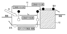
図2は、本願における「有機電子供与体の励起子拡散長」を説明するための概念図である。 FIG. 2 is a conceptual diagram for explaining “exciton diffusion length of an organic electron donor” in the present application.
図2に示すように、本願において、有機電子供与体の励起子拡散長とは、有機電子供与体層11に光を照射することにより、当該層11内に生じる励起子が再結合等によって失活するまでに移動する平均の距離(図2中の符号LP)を意味する。
As shown in FIG. 2, in the present application, the exciton diffusion length of the organic electron donor means that the exciton generated in the organic
この励起子拡散長LPは、以下の方法により算出することができる(図2参照)。 This exciton diffusion length L P can be calculated by the following method (see FIG. 2).
(励起子拡散長LPの算出方法)
(1)光学干渉を考慮し、有機電子供与体層11内部の光学強度分布をマトリックス法にて計算する。
(2)励起子の移動は拡散方程式に従うものとする。
(3)電子受容体層12との界面に達した励起子は、確率ηEDで電子と正孔に分離すると仮定する。
(4)電子受容体層12との界面近傍に蓄積している電子と正孔は、確率ηRで再結合すると仮定する。
(5)電子受容体層12との界面から離れた電子と正孔は、全て電極に回収されると仮定する。
(6)前記(3)〜(5)の仮定により、(取り出したキャリア数)=(1−ηR)×ηED×(界面に到達した励起子数)となり、(1−ηR)×ηEDの値を補正項として纏めてηCとすれば、(取り出したキャリア数)=ηC×(界面に到達した励起子数)となる。
(7)有機電子供与体11へ照射する光の波長を変化させた場合の光電交換効率(EQE(%))を測定しておき、上記(1)〜(6)の条件に基づき得られた算出式中の電子供与体層11の励起子拡散長LP、電子受容体層12の励起子拡散長Ln、さらには前記補正項ηCのそれぞれをパラメータとして、前記測定した光電交換効率(EQE(%))と上記(1)〜(6)の条件に基づき得られた算出式とが一致するように前記各パラメータの値を決定する。
(8)上記(7)で決定された電子供与体層11の励起子拡散長LPを、本願が定義する励起子拡散長とする。
(Calculation method of exciton diffusion length L P )
(1) In consideration of optical interference, the optical intensity distribution inside the organic
(2) The exciton movement follows the diffusion equation.
(3) Assume that interface reaches excitons of the
(4) It is assumed that electrons and holes accumulated near the interface with the
(5) It is assumed that all electrons and holes separated from the interface with the
(6) Based on the assumptions of (3) to (5), (number of extracted carriers) = (1−η R ) × η ED × (number of excitons reaching the interface), and (1−η R ) × When the value of η ED is collectively taken as a correction term and η C , (the number of extracted carriers) = η C × (the number of excitons reaching the interface).
(7) The photoelectric exchange efficiency (EQE (%)) when the wavelength of light irradiated to the
(8) The exciton diffusion length L P of the
上記励起子拡散長LPの算出方法を、具体例を用いて説明すると以下の通りである。 The method for calculating the exciton diffusion length L P will be described below using a specific example.
例えば、有機電子供与体層11を構成する有機電子供与体として鉄フタロシアニンを用い、一方で電子受容体層12を構成する電子受容体としてフラーレンを用いた場合において、上記算出方法(1)〜(6)に基づき計算を行い、次いで上記算出方法(7)に従い、得られた算出式と予め測定した光電交換効率(EQE(%))とが一致するように、鉄フタロシアニンからなる有機電子供与体層11の励起子拡散長LFEPC、フラーレンからなる電子受容体層12の励起子拡散長LC60、および補正項ηCの値を決定した。
For example, in the case where iron phthalocyanine is used as the organic electron donor constituting the organic
その結果を図3(a)に示す。 The result is shown in FIG.
ここで、この具体例においては、フラーレンからなる電子受容体層12の励起子拡散長LC60については変数とせず、40nmに固定して、その他2つ(鉄フタロシアニンからなる有機電子供与体層11の励起子拡散長LFEPCおよび補正項ηC)を変数とした。その結果、図3(a)に示すように、鉄フタロシアニンからなる有機電子供与体層11の励起子拡散長LFEPCを1.0nmとし、補正項ηCを0.14とすると、算出式(図中のプロット)と光電交換効率(EQE(%))の測定値(図中の実線)が一致した。従って、この具体例における有機電子供与体層11の励起子拡散長LFEPCは1.0nmとなり、そうすると、有機電子供与体層11を構成する有機電子供与体として鉄フタロシアニンを用い、一方電子受容体層12を構成する電子受容体としてフラーレンを用いた場合における本願の有機太陽電池にあっては、前記有機電子供与体層11の厚さは、2〜5nmと設計させることとなる。この程度の厚さとすることにより、光の吸収量と電流の流れやすさの双方においてバランスが良い有機電子供与体層11とすることが可能となり、その結果として、光電交換効率に優れた有機太陽電池を提供することが可能となる。
Here, in this specific example, the exciton diffusion length L C60 of the
さらに別の具体例を示す。 Yet another specific example is shown.
有機電子供与体層11を構成する有機電子供与体としてコバルトフタロシアニンを用いた以外は、前記鉄フタロシアニンを用いた場合と全く同様の手順により、コバルトフタロシアニンからなる有機電子供与体層11の励起子拡散長LCOPCを算出した。
Exciton diffusion of the organic
その結果を図3(b)に示す。 The result is shown in FIG.
図3(b)に示すように、コバルトフタロシアニンからなる有機電子供与体層11の励起子拡散長LFEPCを1.6nmとし、補正項ηCを0.17とすると、算出式(図中のプロット)と光電交換効率(EQE(%))の測定値(図中の実線)が一致した。従って、この具体例における有機電子供与体層11の励起子拡散長LCOPCは1.6nmとなり、そうすると、有機電子供与体層11を構成する有機電子供与体としてコバルトフタロシアニンを用い、一方電子受容体層12を構成する電子受容体としてフラーレンを用いた場合における本願の有機太陽電池にあっては、前記有機電子供与体層11の厚さは、1.6〜8.0nmと設計させることとなる。
As shown in FIG. 3B, when the exciton diffusion length LFEPC of the organic
上記と同様にして、有機電子供与体層11を構成する有機電子供与体として、ニッケルフタロシアニン、銅フタロシアニン、亜鉛フタロシアニン、および無金属フタロシアニンのそれぞれを用いて、それぞれの有機電子供与体層11の励起子拡散長LNiPC、LCuPC、LZnPC、LH2PCを算出した。
In the same manner as described above, nickel phthalocyanine, copper phthalocyanine, zinc phthalocyanine, and metal-free phthalocyanine are used as organic electron donors constituting the organic
その結果を図3(c)〜(f)に示す。 The results are shown in FIGS.
図3(c)に示すように、ニッケルフタロシアニンからなる有機電子供与体層11の励起子拡散長LNiPCを9.0nmとし、補正項ηCを0.21とすると、算出式(図中のプロット)と光電交換効率(EQE(%))の測定値(図中の実線)が一致した。従って、この具体例における有機電子供与体層11の励起子拡散長LNiPCは9.0nmとなり、そうすると、有機電子供与体層11を構成する有機電子供与体としてニッケルフタロシアニンを用い、一方電子受容体層12を構成する電子受容体としてフラーレンを用いた場合における本願の有機太陽電池にあっては、前記有機電子供与体層11の厚さは、18.0〜45.0nmと設計させることとなる。
As shown in FIG. 3C, when the exciton diffusion length L NiPC of the organic
また、図3(d)に示すように、銅フタロシアニンからなる有機電子供与体層11の励起子拡散長LCuPCを15.4nmとし、補正項ηCを0.33とすると、算出式(図中のプロット)と光電交換効率(EQE(%))の測定値(図中の実線)が一致した。従って、この具体例における有機電子供与体層11の励起子拡散長LCuPCは15.4nmとなり、そうすると、有機電子供与体層11を構成する有機電子供与体として銅フタロシアニンを用い、一方電子受容体層12を構成する電子受容体としてフラーレンを用いた場合における本願の有機太陽電池にあっては、前記有機電子供与体層11の厚さは、30.8〜77.0nmと設計させることとなる。
Further, as shown in FIG. 3D , when the exciton diffusion length L CuPC of the organic
また、図3(e)に示すように、亜鉛フタロシアニンからなる有機電子供与体層11の励起子拡散長LZnPCを15.0nmとし、補正項ηCを0.33とすると、算出式(図中のプロット)と光電交換効率(EQE(%))の測定値(図中の実線)が一致した。従って、この具体例における有機電子供与体層11の励起子拡散長LZnPCは15.0nmとなり、そうすると、有機電子供与体層11を構成する有機電子供与体として亜鉛フタロシアニンを用い、一方電子受容体層12を構成する電子受容体としてフラーレンを用いた場合における本願の有機太陽電池にあっては、前記有機電子供与体層11の厚さは、30.0〜75.0nmと設計させることとなる。
Further, as shown in FIG. 3E, when the exciton diffusion length L ZnPC of the organic
また、図3(f)に示すように、無金属フタロシアニンからなる有機電子供与体層11の励起子拡散長LH2PCを11.9nmとし、補正項ηCを0.34とすると、算出式(図中のプロット)と光電交換効率(EQE(%))の測定値(図中の実線)が一致した。従って、この具体例における有機電子供与体層11の励起子拡散長LH2PCは11.9nmとなり、そうすると、有機電子供与体層11を構成する有機電子供与体として無金属フタロシアニンを用い、一方電子受容体層12を構成する電子受容体としてフラーレンを用いた場合における本願の有機太陽電池にあっては、前記有機電子供与体層11の厚さは、23.8〜59.5nmと設計させることとなる。
Further, as shown in FIG. 3F , when the exciton diffusion length L H2PC of the organic
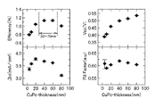
ここで、本願発明の効果を別の具体例を挙げて説明する。 Here, the effect of the present invention will be described with another specific example.
陽極14としてITO、陰極15として銀を用い、さらに有機電子供与体層11を構成する有機電子供与体として前記銅フタロシアニンを用い、電子受容体層12を構成する電子受容体としてフラーレンを用いて、図1に示すような有機太陽電池10を実際に形成した。この際、陽極14の厚さを110nm、陰極15の厚さを50nm、さらに電子受容体層12の厚さを30nmに固定し、銅フタロシアニンからなる有機電子供与体層11の厚さのみを5、10、20、40、60、80nmに変化させて形成し、それぞれの有機太陽電池10について、光電交換効率、短絡電流値(Jsc)、開放電圧値(Voc)、およびフィルファクター値を測定することにより、有機電子供与体層11の厚さの影響を調べた。
Using ITO as the
その結果を図4に示す。 The result is shown in FIG.
図4からも明らかなように、光電交換効率、短絡電流値(Jsc)、開放電圧値(Voc)、およびフィルファクター値は全て、有機電子供与体層11の厚さの関数となっており、それぞれが別個独立した挙動を示すことが明らかになった。ここで、光電交換効率に注目すると、有機電子供与体層11の厚さが30〜70nmの時に有機太陽電池の光電交換効率は最大値を示しており、この厚さは、前記有機電子供与体層11の励起子拡散長励起子拡散長LCuPCから算出した値(30.8〜77.0nm)とほぼ一致している。このことからも、本願の有機太陽電池によれば、有機電子供与体層11の厚さをその励起子拡散長に基づき設計することにより、有機電子供与体層11の光の吸収量と電流の流れやすさの双方においてバランスが良い有機電子供与体層11とすることが可能となり、その結果として、光電交換効率に優れた有機太陽電池を提供することが可能となることが分かる。また、本願の有機太陽電池10にあっては、前記の通り、有機電子供与体層11の厚さを、これを構成する有機電子供与体の励起子拡散長のみに基づき設定可能であるので、有機太陽電池の性能を表す種々のパラメータ(例えば、短絡電流値(Jsc)、開放電圧値(Voc)、およびフィルファクター値など)を測定することなく、従って、有機太陽電池の設計が容易になることが分かる。
As is clear from FIG. 4, the photoelectric exchange efficiency, the short-circuit current value (Jsc), the open-circuit voltage value (Voc), and the fill factor value are all functions of the thickness of the organic
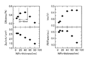
前記と同様の方法により、有機電子供与体層11を構成する有機電子供与体として前記ニッケルフタロシアニンを用いた場合についても確認してみた。
The same method as described above was used to confirm the case where the nickel phthalocyanine was used as the organic electron donor constituting the organic
その結果を図5に示す。 The result is shown in FIG.
前記と同様に光電交換効率に注目すると、有機電子供与体層11の厚さが20〜50nmの時に有機太陽電池の光電交換効率は最大値を示しており、この厚さは、前記有機電子供与体層11の励起子拡散長励起子拡散長LNiPCから算出した値(18.0〜45.0nm)とほぼ一致しており、前記銅フタロシアニンの場合と同様のことが言える。
以上説明したように、本願の有機太陽電池にあっては、前記有機電子供与体層の厚さを、これを構成する有機電子供与体の励起子拡散長の2〜5倍とすることにより、換言すれば、有機電子供与体層の厚さをその励起子拡散長に基づき設計することにより、有機電子供与体層の光の吸収量と電流の流れやすさの双方においてバランスが良い有機電子供与体層とすることが可能となり、その結果として、光電交換効率に優れた有機太陽電池を提供することが可能となる。
If attention is paid to the photoelectric exchange efficiency as described above, the photoelectric exchange efficiency of the organic solar cell shows the maximum value when the thickness of the organic
As described above, in the organic solar cell of the present application, by setting the thickness of the organic electron donor layer to 2 to 5 times the exciton diffusion length of the organic electron donor constituting the organic solar cell, In other words, by designing the thickness of the organic electron donor layer based on the exciton diffusion length, the organic electron donor layer has a good balance between the light absorption amount and the current flowability of the organic electron donor layer. As a result, it is possible to provide an organic solar cell excellent in photoelectric exchange efficiency.
また、本願の有機太陽電池にあっては、前記の通り、有機電子供与体層の厚さを、これを構成する有機電子供与体の励起子拡散長のみに基づき設定可能であるので、有機太陽電池の性能を表す種々のパラメータ(例えば、短絡電流値(Jsc)、開放電圧値(Voc)、およびフィルファクター値など)を測定することなく、従って、有機太陽電池の設計が容易になる。 In the organic solar cell of the present application, as described above, the thickness of the organic electron donor layer can be set based only on the exciton diffusion length of the organic electron donor constituting the organic solar donor layer. Without measuring various parameters representing the performance of the battery (for example, short circuit current value (Jsc), open circuit voltage value (Voc), fill factor value, etc.), the design of the organic solar cell is facilitated.
10 … 有機太陽電池
11 … 有機電子供与体層
12 … 電子受容体層
13 … 光電変換層
14 … 電極(陽極)
15 … 電極(陰極)
16 … 基板
DESCRIPTION OF
15 ... Electrode (cathode)
16 ... Board
Claims (4)
前記有機電子供与体層の厚さが、これを構成する有機電子供与体の励起子拡散長の2〜5倍であることを特徴とする有機太陽電池。 An organic solar cell comprising at least a photoelectric conversion layer having a heterojunction formed from an organic electron donor layer and an electron acceptor layer, and a pair of electrodes sandwiching the photoelectric conversion layer,
An organic solar cell characterized in that the thickness of the organic electron donor layer is 2 to 5 times the exciton diffusion length of the organic electron donor constituting the organic electron donor layer.
Priority Applications (1)
| Application Number | Priority Date | Filing Date | Title |
|---|---|---|---|
| JP2006077509A JP2007258263A (en) | 2006-03-20 | 2006-03-20 | Organic solar cell |
Applications Claiming Priority (1)
| Application Number | Priority Date | Filing Date | Title |
|---|---|---|---|
| JP2006077509A JP2007258263A (en) | 2006-03-20 | 2006-03-20 | Organic solar cell |
Publications (1)
| Publication Number | Publication Date |
|---|---|
| JP2007258263A true JP2007258263A (en) | 2007-10-04 |
Family
ID=38632225
Family Applications (1)
| Application Number | Title | Priority Date | Filing Date |
|---|---|---|---|
| JP2006077509A Pending JP2007258263A (en) | 2006-03-20 | 2006-03-20 | Organic solar cell |
Country Status (1)
| Country | Link |
|---|---|
| JP (1) | JP2007258263A (en) |
Cited By (3)
| Publication number | Priority date | Publication date | Assignee | Title |
|---|---|---|---|---|
| WO2009089470A2 (en) * | 2008-01-11 | 2009-07-16 | Massachusetts Institute Of Technology | Photovoltaic devices |
| JP2009283914A (en) * | 2008-04-24 | 2009-12-03 | Toray Ind Inc | Material for photovoltaic element and the photovoltaic element |
| JP2011513962A (en) * | 2008-02-29 | 2011-04-28 | インターナショナル・ビジネス・マシーンズ・コーポレーション | Photovoltaic devices using high aspect ratio nanostructures and methods for making the same |
Citations (4)
| Publication number | Priority date | Publication date | Assignee | Title |
|---|---|---|---|---|
| JPH05335614A (en) * | 1992-06-03 | 1993-12-17 | Idemitsu Kosan Co Ltd | Photoelectric conversion element |
| JPH0974216A (en) * | 1995-09-07 | 1997-03-18 | Nippon Shokubai Co Ltd | Organic solar battery |
| JP2002523904A (en) * | 1998-08-19 | 2002-07-30 | ザ、トラスティーズ オブ プリンストン ユニバーシティ | Organic photosensitive optoelectronic devices |
| WO2005101524A2 (en) * | 2004-04-13 | 2005-10-27 | The Trustees Of Princeton University | Method of fabricating an optoelectronic device having a bulk heterojunction |
-
2006
- 2006-03-20 JP JP2006077509A patent/JP2007258263A/en active Pending
Patent Citations (4)
| Publication number | Priority date | Publication date | Assignee | Title |
|---|---|---|---|---|
| JPH05335614A (en) * | 1992-06-03 | 1993-12-17 | Idemitsu Kosan Co Ltd | Photoelectric conversion element |
| JPH0974216A (en) * | 1995-09-07 | 1997-03-18 | Nippon Shokubai Co Ltd | Organic solar battery |
| JP2002523904A (en) * | 1998-08-19 | 2002-07-30 | ザ、トラスティーズ オブ プリンストン ユニバーシティ | Organic photosensitive optoelectronic devices |
| WO2005101524A2 (en) * | 2004-04-13 | 2005-10-27 | The Trustees Of Princeton University | Method of fabricating an optoelectronic device having a bulk heterojunction |
Cited By (5)
| Publication number | Priority date | Publication date | Assignee | Title |
|---|---|---|---|---|
| WO2009089470A2 (en) * | 2008-01-11 | 2009-07-16 | Massachusetts Institute Of Technology | Photovoltaic devices |
| WO2009089470A3 (en) * | 2008-01-11 | 2009-10-08 | Massachusetts Institute Of Technology | Photovoltaic devices |
| US8525022B2 (en) | 2008-01-11 | 2013-09-03 | Massachusetts Institute Of Technology | High efficiency multi-layer photovoltaic devices |
| JP2011513962A (en) * | 2008-02-29 | 2011-04-28 | インターナショナル・ビジネス・マシーンズ・コーポレーション | Photovoltaic devices using high aspect ratio nanostructures and methods for making the same |
| JP2009283914A (en) * | 2008-04-24 | 2009-12-03 | Toray Ind Inc | Material for photovoltaic element and the photovoltaic element |
Similar Documents
| Publication | Publication Date | Title |
|---|---|---|
| Chowdhury et al. | Stability of perovskite solar cells: issues and prospects | |
| de la Torre et al. | Phthalocyanines and subphthalocyanines: Perfect partners for fullerenes and carbon nanotubes in molecular photovoltaics | |
| Jeon et al. | Metal-electrode-free window-like organic solar cells with p-doped carbon nanotube thin-film electrodes | |
| Yum et al. | Recent developments in solid‐state dye‐sensitized solar cells | |
| US8592804B2 (en) | Method for fabricating organic optoelectronic devices | |
| Batmunkh et al. | Single-walled carbon nanotubes enhance the efficiency and stability of mesoscopic perovskite solar cells | |
| Li et al. | Polyethyleneimine high-energy hydrophilic surface interfacial treatment toward efficient and stable perovskite solar cells | |
| Lee et al. | Toward visibly transparent organic photovoltaic cells based on a near-infrared harvesting bulk heterojunction blend | |
| Upama et al. | Role of fullerene electron transport layer on the morphology and optoelectronic properties of perovskite solar cells | |
| Samanta et al. | Role of various transport layer and electrode materials in enhancing performance of stable environment-friendly Cs2TiBr6 solar cell | |
| JP6763560B2 (en) | Manufacturing method of organic-inorganic composite solar cell and organic-inorganic composite solar cell | |
| TW201517343A (en) | Exciton-blocking treatments for buffer layers in organic photovoltaics | |
| Reddy et al. | Metallated macrocyclic derivatives as a hole–transporting materials for perovskite solar cells | |
| CA2880519A1 (en) | Organic optoelectronics with electrode buffer layers | |
| CN102939673A (en) | Enhanced bulk heterojunction devices prepared by thermal and solvent vapor annealing processes | |
| Torimtubun et al. | Fluorinated Zinc and Copper phthalocyanines as efficient third components in ternary bulk heterojunction solar cells | |
| Ramachandran et al. | Recent progress in electrode fabrication materials and various insights in solar cells | |
| Lu et al. | Multiple roles of cobalt pyrazol-pyridine complexes in high-performing perovskite solar cells | |
| Lv et al. | Elimination of charge transport layers in high-performance perovskite solar cells by band bending | |
| JP2015526901A (en) | Multi-junction organic solar cells using active layers deposited by solution processing and vacuum evaporation | |
| Baumeler et al. | Champion Device Architectures for Low-Cost and Stable Single-Junction Perovskite Solar Cells | |
| Zhang et al. | Employing easily prepared carbon nanoparticles to improve performance of inverted organic solar cells | |
| JP2007258263A (en) | Organic solar cell | |
| JP5872831B2 (en) | Photovoltaic device | |
| WO2013102985A1 (en) | Organic photoelectric conversion element and organic thin-film solar battery module |
Legal Events
| Date | Code | Title | Description |
|---|---|---|---|
| A621 | Written request for application examination |
Free format text: JAPANESE INTERMEDIATE CODE: A621 Effective date: 20090206 |
|
| A977 | Report on retrieval |
Free format text: JAPANESE INTERMEDIATE CODE: A971007 Effective date: 20101125 |
|
| A131 | Notification of reasons for refusal |
Free format text: JAPANESE INTERMEDIATE CODE: A131 Effective date: 20101130 |
|
| A02 | Decision of refusal |
Free format text: JAPANESE INTERMEDIATE CODE: A02 Effective date: 20110405 |